EP4303579A1 - Detection device - Google Patents
Detection device Download PDFInfo
- Publication number
- EP4303579A1 EP4303579A1 EP22763054.8A EP22763054A EP4303579A1 EP 4303579 A1 EP4303579 A1 EP 4303579A1 EP 22763054 A EP22763054 A EP 22763054A EP 4303579 A1 EP4303579 A1 EP 4303579A1
- Authority
- EP
- European Patent Office
- Prior art keywords
- magnetic
- excitation
- detection device
- opening end
- excitation coil
- Prior art date
- Legal status (The legal status is an assumption and is not a legal conclusion. Google has not performed a legal analysis and makes no representation as to the accuracy of the status listed.)
- Pending
Links
- 238000001514 detection method Methods 0.000 title claims abstract description 100
- 230000005284 excitation Effects 0.000 claims abstract description 105
- 230000004907 flux Effects 0.000 claims abstract description 51
- 230000000704 physical effect Effects 0.000 claims abstract description 15
- 230000035945 sensitivity Effects 0.000 description 10
- 230000008859 change Effects 0.000 description 9
- 239000000843 powder Substances 0.000 description 3
- 230000008878 coupling Effects 0.000 description 2
- 238000010168 coupling process Methods 0.000 description 2
- 238000005859 coupling reaction Methods 0.000 description 2
- 238000010586 diagram Methods 0.000 description 2
- 230000007613 environmental effect Effects 0.000 description 2
- 230000007274 generation of a signal involved in cell-cell signaling Effects 0.000 description 2
- 230000004048 modification Effects 0.000 description 2
- 238000012986 modification Methods 0.000 description 2
- 239000012141 concentrate Substances 0.000 description 1
- 230000000694 effects Effects 0.000 description 1
- 230000005415 magnetization Effects 0.000 description 1
- 239000000463 material Substances 0.000 description 1
- 239000002184 metal Substances 0.000 description 1
- 229910000889 permalloy Inorganic materials 0.000 description 1
- 230000035699 permeability Effects 0.000 description 1
- 229910000859 α-Fe Inorganic materials 0.000 description 1
Images






Classifications
-
- G—PHYSICS
- G01—MEASURING; TESTING
- G01N—INVESTIGATING OR ANALYSING MATERIALS BY DETERMINING THEIR CHEMICAL OR PHYSICAL PROPERTIES
- G01N27/00—Investigating or analysing materials by the use of electric, electrochemical, or magnetic means
- G01N27/72—Investigating or analysing materials by the use of electric, electrochemical, or magnetic means by investigating magnetic variables
- G01N27/82—Investigating or analysing materials by the use of electric, electrochemical, or magnetic means by investigating magnetic variables for investigating the presence of flaws
-
- G—PHYSICS
- G01—MEASURING; TESTING
- G01N—INVESTIGATING OR ANALYSING MATERIALS BY DETERMINING THEIR CHEMICAL OR PHYSICAL PROPERTIES
- G01N27/00—Investigating or analysing materials by the use of electric, electrochemical, or magnetic means
- G01N27/72—Investigating or analysing materials by the use of electric, electrochemical, or magnetic means by investigating magnetic variables
- G01N27/82—Investigating or analysing materials by the use of electric, electrochemical, or magnetic means by investigating magnetic variables for investigating the presence of flaws
- G01N27/83—Investigating or analysing materials by the use of electric, electrochemical, or magnetic means by investigating magnetic variables for investigating the presence of flaws by investigating stray magnetic fields
- G01N27/87—Investigating or analysing materials by the use of electric, electrochemical, or magnetic means by investigating magnetic variables for investigating the presence of flaws by investigating stray magnetic fields using probes
-
- G—PHYSICS
- G01—MEASURING; TESTING
- G01R—MEASURING ELECTRIC VARIABLES; MEASURING MAGNETIC VARIABLES
- G01R33/00—Arrangements or instruments for measuring magnetic variables
- G01R33/0011—Arrangements or instruments for measuring magnetic variables comprising means, e.g. flux concentrators, flux guides, for guiding or concentrating the magnetic flux, e.g. to the magnetic sensor
-
- G—PHYSICS
- G01—MEASURING; TESTING
- G01R—MEASURING ELECTRIC VARIABLES; MEASURING MAGNETIC VARIABLES
- G01R33/00—Arrangements or instruments for measuring magnetic variables
- G01R33/0017—Means for compensating offset magnetic fields or the magnetic flux to be measured; Means for generating calibration magnetic fields
-
- G—PHYSICS
- G01—MEASURING; TESTING
- G01R—MEASURING ELECTRIC VARIABLES; MEASURING MAGNETIC VARIABLES
- G01R33/00—Arrangements or instruments for measuring magnetic variables
- G01R33/02—Measuring direction or magnitude of magnetic fields or magnetic flux
-
- G—PHYSICS
- G01—MEASURING; TESTING
- G01R—MEASURING ELECTRIC VARIABLES; MEASURING MAGNETIC VARIABLES
- G01R33/00—Arrangements or instruments for measuring magnetic variables
- G01R33/02—Measuring direction or magnitude of magnetic fields or magnetic flux
- G01R33/06—Measuring direction or magnitude of magnetic fields or magnetic flux using galvano-magnetic devices
-
- G—PHYSICS
- G01—MEASURING; TESTING
- G01R—MEASURING ELECTRIC VARIABLES; MEASURING MAGNETIC VARIABLES
- G01R33/00—Arrangements or instruments for measuring magnetic variables
- G01R33/02—Measuring direction or magnitude of magnetic fields or magnetic flux
- G01R33/06—Measuring direction or magnitude of magnetic fields or magnetic flux using galvano-magnetic devices
- G01R33/09—Magnetoresistive devices
Definitions
- the present invention relates to a detection device and, more particularly, to a detection device that applies magnetic flux to an object to be inspected to detect a physical property.
- a change in magnetic flux can be detected by using a magnetic sensor described in Patent Document 1, for example.
- Patent Document 1 Japanese Patent No. 6,610,178
- Patent Document 1 has sensitivity to magnetic flux over a relatively wide range and is thus not suitable for detecting the physical property of an object to be inspected within a narrow area.
- a detection device includes first and second excitation coils each wound such that magnetic flux generated in the inner diameter area thereof flows out from one opening end thereof toward the other opening end, a magnetic member that induces magnetic flux from the other opening end of the second excitation coil to the one opening end of the first excitation coil, and a magnetic detection part that detects magnetic flux flowing through the magnetic member. Magnetic flux flowing out from the other opening end of the first excitation coil to the one opening end of the second excitation coil is applied to an object to be inspected to detect the physical property of the object to be inspected is detected.
- the first and second excitation coils generating magnetic fluxes flowing in mutually reverse directions are used, so that magnetic flux can be concentrated within a relatively narrow area of the object to be inspected. This allows detection of the physical property of the object to be inspected within a relatively narrow area.
- the first and second excitation coils may be connected in series to each other and whereby the same excitation current may flow in the first and second excitation coils. This simplifies a circuit configuration.
- the magnetic member may include a first magnetic member magnetically coupled to the first excitation coil and a second magnetic member magnetically coupled to the second excitation coil, and the magnetic detection part may detect magnetic flux flowing between the first and second magnetic members. This allows the magnetic detection part to detect a change in the magnetic flux with high sensitivity.
- a part of the first magnetic member may be positioned in the inner diameter area of the first excitation coil, and a part of the second magnetic member may be positioned in the inner diameter area of the second excitation coil. This allows further enhancement of detection sensitivity.
- the coil axes of the respective first and second excitation coils may be positioned on a first virtual plane
- the coil axis of the first excitation coil may further be positioned on a second virtual plane perpendicular to the first virtual plane
- the coil axis of the second excitation coil may further be positioned on a third virtual plane perpendicular to the second virtual plane
- the magnetic detection part may be positioned between the second and third virtual planes. This allows the magnetic detection part to detect a change in magnetic flux with high sensitivity.
- the detection device may further include an excitation circuit for making an excitation current flow through the first and second excitation coils based on a search signal having a predetermined frequency, a high-pass filter for removing a low frequency component from an output signal of the magnetic detection part, and a detection circuit for detecting an output signal of the high-pass filter based on the search signal. This can eliminate the influence of a magnetic field emitted from the object to be inspected or an environmental magnetic field.
- a detection device capable of detecting the physical property of an object to be inspected within a relatively narrow area.
- FIG. 1 is a schematic view for explaining the structure of a detection device 1 according to a first embodiment of the present invention, where FIG. 1A is an xz side view, and FIG. 1B is an xy plan view.
- the detection device 1 is configured to detect the physical property of an object A to be inspected and includes excitation coils 10 and 20 whose axial direction is the z-direction, magnetic members 31 and 32 disposed respectively at positions overlapping the coil axes of the respective excitation coils 10 and 20, and a magnetic detection part 40 disposed between the magnetic members 31 and 32.
- the excitation coils 10 and 20 are connected in series to each other and are wound in mutually reverse directions.
- the magnetic flux flows through a relatively narrow space from the opening end 12 of the excitation coil 10 to the opening end 21 of the excitation coil 20.
- the magnetic flux flows through a relatively narrow space from the opening end 22 of the excitation coil 20 to the opening end 11 of the excitation coil 10.
- the magnetic members 31 and 32 are made of a high permeability material such as ferrite. As illustrated in FIGS. 1A and 1B , the magnetic members 31 and 32 are disposed respectively at positions overlapping the coil axes of the respective excitation coils 10 and 20, so that the excitation coil 10 and magnetic member 31 are magnetically coupled to each other, and the excitation coil 20 and magnetic member 32 are magnetically coupled to each other. Thus, the magnetic flux emerging from the opening end 22 of the excitation coil 20 flows to the opening end 11 of the excitation coil 10 while being induced by the magnetic members 31 and 32. Since the magnetic detection part 40 is disposed between the magnetic members 31 and 32, the magnetic flux flowing between the magnetic members 31 and 32 is detected by the magnetic detection part 40.
- the magnetic detection part 40 is not particularly limited in position as long as it can detect the magnetic flux flowing between the magnetic members 31 and 32; however, as illustrated in FIG. 1B , assuming that the coil axes of the respective excitation coils 10 and 20 are defined as C1 and C2, that a virtual plane in which both the coil axes C1 and C2 are present is defined as P1, that a virtual plane in which the coil axis C1 is present and which is perpendicular to the virtual plane P1 is defined as P2, and that a virtual plane in which the coil axis C2 is present and which is perpendicular to the virtual plane P1 is defined as P3, the magnetic detection part 40 is preferably disposed between the virtual planes P2 and P3. The magnetic detection part 40 disposed to fall within such an area can detect the magnetic flux generated by the excitation coils 10 and 20 with high sensitivity.
- the detection device 1 can detect the physical property of the object A to be inspected which is disposed at the leading ends of the excitation coils 10 and 20 in the z-direction, that is, in the vicinity of the opening ends 12 and 21 of the respective excitation coils 10 and 20. More specifically, the magnetic flux radiated from the opening end 12 of the excitation coil 10 and absorbed into the opening end 21 of the excitation coil 20 is applied to a predetermined area of the object A to be inspected, and a change in the magnetic flux caused by the applied magnetic flux is detected by the magnetic detection part 40, whereby a magnetic member or a flaw present in the predetermined area of the object A to be inspected can be detected.
- FIG. 2 is a circuit block diagram of the detection device 1 according to the present embodiment.
- the detection device 1 further includes a detection circuit 50.
- the detection circuit 50 includes a search signal generation circuit 51 for generating a search signal S1 having a predetermined frequency, an excitation circuit 52 for making an excitation current I flow through the excitation coils 10 and 20 based on the search signal S1, a high-pass filter 53 for generating an output signal S3 by removing a low frequency component from an output signal S2 of the magnetic detection part 40, and a detection circuit 54 for detecting the output signal S3 of the high-pass filter 53 based on the search signal S1.
- the excitation circuit 52 makes an excitation current I having the same frequency as the search signal S1 having a predetermined frequency flow through the excitation coils 10 and 20.
- the magnetic fluxes ⁇ 1 and ⁇ 2 thus generated are detected by the magnetic detection part 40, and an output signal S2 corresponding to the direction and strength of the magnetic flux is generated.
- the output signal S2 changes correspondingly.
- the occurrence of a change in the magnetic flux to be applied to the magnetic detection part 40 could be attributable to sticking or mixing of magnetic fine powder to or into the object A to be inspected, a change in eddy current due to the presence of a flaw in a metal object as the object A to be inspected, and the like.
- the thus generated output signal S2 of the magnetic detection part 40 is subjected to removal of a low-frequency component by the high-pass filter 53, whereby the output signal S3 is generated. It is not essential to use the high-pass filter in the present invention; however, removal of a low-frequency component using the high-pass filter can eliminate the influence of a magnetic field emitted from the object A to be inspected or an environmental magnetic field.
- the thus generated output signal S3 is detected by the detection circuit 54, whereby an output signal S4 of a DC level is generated.
- an output signal S4 of a DC level is generated.
- the detection device 1 uses the excitation coils 10 and 20 wound in mutually reverse directions, thereby making it possible to concentrate detection magnetic flux within a relatively narrow area of the object A to be inspected.
- the physical property of the object A to be inspected within a relatively narrow area can be detected with high sensitivity.
- FIG. 3 is a schematic xz side view for explaining the structure of a detection device 2 according to a second embodiment of the present invention.
- the detection device 2 according to the second embodiment differs from the detection device 1 according to the first embodiment in that magnetic members 33 and 34 are inserted respectively through the inner diameter areas of the excitation coils 10 and 20.
- Other basic configurations are the same as those of the detection device 1 according to the first embodiment, so the same reference numerals are given to the same elements, and overlapping description will be omitted.
- the magnetic member 33 is positioned close to or in contact with the magnetic member 31, whereby magnetic coupling between the magnetic member 31 and the excitation coil 10 is enhanced.
- the magnetic member 34 is positioned close to or in contact with the magnetic member 32, whereby magnetic coupling between the magnetic member 32 and the excitation coil 20 is enhanced. Adding the thus configured magnetic members 33 and 34 allows further enhancement of detection sensitivity.
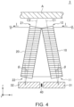
- FIG. 4 is a schematic xz side view for explaining the structure of a detection device 3 according to a third embodiment of the present invention.
- the detection device 3 according to the third embodiment differs from the detection device 1 according to the first embodiment in that the coil axes of the respective excitation coils 10 and 20 have a predetermined inclination with respect to the z-direction.
- Other basic configurations are the same as those of the detection device 1 according to the first embodiment, so the same reference numerals are given to the same elements, and overlapping description will be omitted.
- a coil axis C1 of the excitation coil 10 is inclined at an angle ⁇ in the negative x-direction
- a coil axis C2 of the excitation coil 20 is inclined at an angle ⁇ in the positive x-direction. This further suppresses the spread of magnetic flux in between the opening end 12 of the excitation coil 10 and the opening end 21 of the excitation coil 20, thus allowing detection magnetic flux to be concentrated within a narrower area of the object A to be inspected.
- FIG. 5 is a schematic perspective view for explaining the structure of a detection device 4 according to a fourth embodiment of the present invention.
- the detection device 4 according to the fourth embodiment differs from the detection device 1 according to the first embodiment in that a sensor chip 60 is used as the magnetic detection part and that the magnetic members 31 and 32 are disposed so as to cover an element forming surface 61 of the sensor chip 60.
- Other basic configurations are the same as those of the detection device 1 according to the first embodiment, so the same reference numerals are given to the same elements, and overlapping description will be omitted.
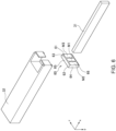
- FIG. 6 is a schematic exploded perspective view illustrating a state where the sensor chip 60 and magnetic members 31, 32 are separated from one another.
- the sensor chip 60 has the element forming surface 61 and a back surface 62 which constitute the yz surface, side surfaces 63 and 64 which constitute the xy surface, and side surfaces 65 and 66 which constitute the xz surface.
- the element forming surface 61 of the sensor chip 60 has mounted thereon a magnetic sensing element (to be described later) and magnetic layers M1 to M3 (to be described later).
- the magnetic member 31 has a bar body elongated in the x-direction, and one end thereof in the x-direction is positioned at substantially the center of the element forming surface 61 in the x-direction so as to cover a part of the magnetic layer M1.
- the magnetic member 32 has a bar body elongated in the x-direction and covers a part of the magnetic layer M2, a part of the magnetic layer M3, and the back and side surfaces 62 and 63 of the sensor chip 60.
- FIG. 7 is a schematic plan view of the sensor chip 60
- FIG. 8 is a schematic cross-sectional view taken along the line B-B in FIG. 7 .
- the magnetic sensing elements R1 to R4 are not particularly limited in type as long as they are elements whose electric resistance varies depending on the direction of magnetic flux and may be an MR element, for example.
- the magnetic sensing elements R1 to R4 have the same fixed magnetization direction (e.g., positive side of the x-direction).
- the magnetic sensing elements R1 to R4 are covered with an insulating layer 67, and magnetic layers M1 to M3 made of permalloy or the like are formed on the surface of the insulating layer 67.
- the magnetic layers M1 to M3 are covered with an insulating layer 68.
- parts of the magnetic layers M1 to M3 that are positioned on one side (upper side in FIG. 7 ) in the y-direction are defined as magnetic layers M11, M21, and M31, respectively, and parts of the magnetic layers M1 to M3 that are positioned on the other side (lower side in FIG.
- the magnetic sensing element R1 is positioned between the magnetic layers M11 and M12 in a plan view (as viewed in the x-direction)
- the magnetic sensing element R2 is positioned between the magnetic layers M12 and M22 in a plan view
- the magnetic sensing element R3 is positioned between the magnetic layers M11 and M31 in a plan view
- the magnetic sensing element R4 is positioned between the magnetic layers M12 and M32 in a plan view.
- the direction of the magnetic fields to be applied to the magnetic sensing elements R1 and R2 and the direction of the magnetic fields to be applied to the magnetic sensing elements R3 and R4 differ from each other by 180°, so that when the magnetic sensing elements R1 to R4 are bridge-connected, the direction and strength of magnetic flux to be applied thereto through the magnetic member 31 can be detected.
- the magnetic sensing elements R1 to R4 are each disposed between two magnetic layers but is sufficient if they are each disposed in the vicinity of each of the magnetic gaps G1 to G4 formed by two magnetic layers, i.e., on a magnetic path formed by each of the magnetic gaps G1 to G4.
- the width of each of the magnetic gaps G1 to G4 need not necessarily be larger but may be smaller than the width of each of the magnetic sensing elements R1 to R4.
- a reference sign 31a denotes an area covered with the magnetic member 31
- reference signs 32a and 32b denote areas each covered with the magnetic member 32.
- the magnetic member 31 covers the magnetic layer M1
- the magnetic member 32 covers the magnetic layers M2 and M3.
- the excitation coils 10 and 20 are magnetically coupled respectively to the magnetic members 31 and 32, so that magnetic fine powder or a flaw present in the object A to be inspected can be detected with high sensitivity.
- FIG. 9 is a schematic perspective view for explaining the structure of a detection device 5 according to a fifth embodiment of the present invention.
- the detection device 5 according to the fifth embodiment differs from the detection device 4 according to the fourth embodiment in that the magnetic members 31 and 32 are partly bent in the z-direction and inserted through the inner diameter areas of the respective excitation coils 10 and 20.
- Other basic configurations are the same as those of the detection device 4 according to the fourth embodiment, so the same reference numerals are given to the same elements, and overlapping description will be omitted.
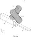
- FIG. 10 is a schematic perspective view illustrating the structure of a detection device 6 according to a sixth embodiment of the present invention.
- a detection device 6 according to the sixth embodiment differs from the detection device 4 according to the fourth embodiment in that the coil axes of the respective excitation coils 10 and 20 have a predetermined inclination with respect to the z-direction.
- Other basic configurations are the same as those of the detection device 4 according to the fourth embodiment, so the same reference numerals are given to the same elements, and overlapping description will be omitted.
- FIG. 11 is a schematic perspective view for explaining the structure of a detection device 7 according to a seventh embodiment of the present invention.
- the detection device 7 according to the seventh embodiment differs from the detection device 4 according to the fourth embodiment in that four excitation coils 10A, 10B, 20A, and 20B are used.
- Other basic configurations are the same as those of the detection device 4 according to the fourth embodiment, so the same reference numerals are given to the same elements, and overlapping description will be omitted.
- the excitation coils 10A and 10B are wound in mutually reverse directions, and the excitation coils 20A and 20B are wound in mutually reverse directions.
- the excitation coils 10A and 10B are magnetically coupled to the magnetic member 31, and the excitation coils 20A and 20B are magnetically coupled to the magnetic member 32.
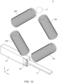
- FIG. 12 is a schematic perspective view for explaining the structure of a detection device 8 according to the present invention.
- the detection device 8 according to the eighth embodiment differs from the detection device 7 according to the seventh embodiment in that the four excitation coils 10A, 10B, 20A, and 20B are disposed such that magnetic flux circulates through the excitation coils 10A, 10B, 20B, and 20A in this order (or its reverse direction).
- Other basic configurations are the same as those of the detection device 7 according to the seventh embodiment, so the same reference numerals are given to the same elements, and overlapping description will be omitted.
- the physical property of the object A to be inspected can be detected with high sensitivity.
Landscapes
- Physics & Mathematics (AREA)
- Chemical & Material Sciences (AREA)
- General Physics & Mathematics (AREA)
- Health & Medical Sciences (AREA)
- Chemical Kinetics & Catalysis (AREA)
- Electrochemistry (AREA)
- Life Sciences & Earth Sciences (AREA)
- Analytical Chemistry (AREA)
- Biochemistry (AREA)
- General Health & Medical Sciences (AREA)
- Immunology (AREA)
- Pathology (AREA)
- Condensed Matter Physics & Semiconductors (AREA)
- Investigating Or Analyzing Materials By The Use Of Magnetic Means (AREA)
Abstract
Description
- The present invention relates to a detection device and, more particularly, to a detection device that applies magnetic flux to an object to be inspected to detect a physical property.
- For detecting the physical property of an object to be inspected, it can be considered to apply magnetic flux to an object to be inspected to detect a change in the magnetic flux. A change in magnetic flux can be detected by using a magnetic sensor described in
Patent Document 1, for example. - [Patent Document 1]
Japanese Patent No. 6,610,178 - However, the magnetic sensor described in
Patent Document 1 has sensitivity to magnetic flux over a relatively wide range and is thus not suitable for detecting the physical property of an object to be inspected within a narrow area. - It is therefore an object of the present invention to provide a detection device capable of detecting the physical property of an object to be inspected within a relatively narrow area.
- A detection device according to the present invention includes first and second excitation coils each wound such that magnetic flux generated in the inner diameter area thereof flows out from one opening end thereof toward the other opening end, a magnetic member that induces magnetic flux from the other opening end of the second excitation coil to the one opening end of the first excitation coil, and a magnetic detection part that detects magnetic flux flowing through the magnetic member. Magnetic flux flowing out from the other opening end of the first excitation coil to the one opening end of the second excitation coil is applied to an object to be inspected to detect the physical property of the object to be inspected is detected.
- According to the present invention, the first and second excitation coils generating magnetic fluxes flowing in mutually reverse directions are used, so that magnetic flux can be concentrated within a relatively narrow area of the object to be inspected. This allows detection of the physical property of the object to be inspected within a relatively narrow area.
- In the present invention, the first and second excitation coils may be connected in series to each other and whereby the same excitation current may flow in the first and second excitation coils. This simplifies a circuit configuration.
- In the present invention, the magnetic member may include a first magnetic member magnetically coupled to the first excitation coil and a second magnetic member magnetically coupled to the second excitation coil, and the magnetic detection part may detect magnetic flux flowing between the first and second magnetic members. This allows the magnetic detection part to detect a change in the magnetic flux with high sensitivity. In this case, a part of the first magnetic member may be positioned in the inner diameter area of the first excitation coil, and a part of the second magnetic member may be positioned in the inner diameter area of the second excitation coil. This allows further enhancement of detection sensitivity.
- In the present invention, the coil axes of the respective first and second excitation coils may be positioned on a first virtual plane, the coil axis of the first excitation coil may further be positioned on a second virtual plane perpendicular to the first virtual plane, the coil axis of the second excitation coil may further be positioned on a third virtual plane perpendicular to the second virtual plane, and the magnetic detection part may be positioned between the second and third virtual planes. This allows the magnetic detection part to detect a change in magnetic flux with high sensitivity.
- The detection device according to the present invention may further include an excitation circuit for making an excitation current flow through the first and second excitation coils based on a search signal having a predetermined frequency, a high-pass filter for removing a low frequency component from an output signal of the magnetic detection part, and a detection circuit for detecting an output signal of the high-pass filter based on the search signal. This can eliminate the influence of a magnetic field emitted from the object to be inspected or an environmental magnetic field.
- As described above, according to the present invention, there can be provided a detection device capable of detecting the physical property of an object to be inspected within a relatively narrow area.
-
-
FIG. 1 is a schematic view for explaining the structure of adetection device 1 according to a first embodiment of the present invention, whereFIG. 1A is an xz side view, andFIG. 1B is an xy plan view. -
FIG. 2 is a circuit block diagram of thedetection device 1. -
FIG. 3 is a schematic xz side view for explaining the structure of adetection device 2 according to a second embodiment of the present invention. -
FIG. 4 is a schematic xz side view for explaining the structure of adetection device 3 according to a third embodiment of the present invention. -
FIG. 5 is a schematic perspective view for explaining the structure of adetection device 4 according to a fourth embodiment of the present invention. -
FIG. 6 is a schematic exploded perspective view illustrating a state where thesensor chip 60 andmagnetic members -
FIG. 7 is a schematic plan view of thesensor chip 60. -
FIG. 8 is a schematic cross-sectional view taken along the line B-B inFIG. 7 . -
FIG. 9 is a schematic perspective view for explaining the structure of adetection device 5 according to a fifth embodiment of the present invention. -
FIG. 10 is a schematic perspective view illustrating the structure of adetection device 6 according to a sixth embodiment of the present invention. -
FIG. 11 is a schematic perspective view for explaining the structure of adetection device 7 according to a seventh embodiment of the present invention. -
FIG. 12 is a schematic perspective view for explaining the structure of adetection device 8 according to the present invention. - Hereinafter, preferred embodiments of the present invention will be described in detail with reference to the accompanying drawings.
-
FIG. 1 is a schematic view for explaining the structure of adetection device 1 according to a first embodiment of the present invention, whereFIG. 1A is an xz side view, andFIG. 1B is an xy plan view. - As illustrated in
FIGS. 1A and 1B , thedetection device 1 according to the first embodiment is configured to detect the physical property of an object A to be inspected and includesexcitation coils magnetic members respective excitation coils magnetic detection part 40 disposed between themagnetic members excitation coils excitation coils excitation coil 10, and a negative z-direction magnetic flux φ2 is generated in the inner diameter area of theexcitation coil 20. As a result, in the inner diameter area of theexcitation coil 10, the magnetic flux φ1 flows from anopening end 11 of theexcitation coil 10 toward anopening end 12 thereof; on the other hand, in the inner diameter area of theexcitation coil 20, the magnetic flux φ2 flows from anopening end 21 of theexcitation coil 20 toward anopening end 22 thereof. - Since the
excitation coils opening end 12 of theexcitation coil 10 to theopening end 21 of theexcitation coil 20. Similarly, the magnetic flux flows through a relatively narrow space from theopening end 22 of theexcitation coil 20 to theopening end 11 of theexcitation coil 10. - The
magnetic members FIGS. 1A and 1B , themagnetic members respective excitation coils excitation coil 10 andmagnetic member 31 are magnetically coupled to each other, and theexcitation coil 20 andmagnetic member 32 are magnetically coupled to each other. Thus, the magnetic flux emerging from theopening end 22 of theexcitation coil 20 flows to theopening end 11 of theexcitation coil 10 while being induced by themagnetic members magnetic detection part 40 is disposed between themagnetic members magnetic members magnetic detection part 40. - The
magnetic detection part 40 is not particularly limited in position as long as it can detect the magnetic flux flowing between themagnetic members FIG. 1B , assuming that the coil axes of therespective excitation coils magnetic detection part 40 is preferably disposed between the virtual planes P2 and P3. Themagnetic detection part 40 disposed to fall within such an area can detect the magnetic flux generated by theexcitation coils - The
detection device 1 according to the present embodiment can detect the physical property of the object A to be inspected which is disposed at the leading ends of theexcitation coils opening ends respective excitation coils end 12 of theexcitation coil 10 and absorbed into the openingend 21 of theexcitation coil 20 is applied to a predetermined area of the object A to be inspected, and a change in the magnetic flux caused by the applied magnetic flux is detected by themagnetic detection part 40, whereby a magnetic member or a flaw present in the predetermined area of the object A to be inspected can be detected. -
FIG. 2 is a circuit block diagram of thedetection device 1 according to the present embodiment. - As illustrated in
FIG. 2 , thedetection device 1 according to the present embodiment further includes adetection circuit 50. Thedetection circuit 50 includes a searchsignal generation circuit 51 for generating a search signal S1 having a predetermined frequency, anexcitation circuit 52 for making an excitation current I flow through the excitation coils 10 and 20 based on the search signal S1, a high-pass filter 53 for generating an output signal S3 by removing a low frequency component from an output signal S2 of themagnetic detection part 40, and adetection circuit 54 for detecting the output signal S3 of the high-pass filter 53 based on the search signal S1. - The
excitation circuit 52 makes an excitation current I having the same frequency as the search signal S1 having a predetermined frequency flow through the excitation coils 10 and 20. The magnetic fluxes φ1 and φ2 thus generated are detected by themagnetic detection part 40, and an output signal S2 corresponding to the direction and strength of the magnetic flux is generated. At this time, when a change occurs in the magnetic flux to be applied to themagnetic detection part 40 by bringing the leading ends of the respective excitation coils 10 and 20 in the z-direction close to the object A to be inspected, the output signal S2 changes correspondingly. The occurrence of a change in the magnetic flux to be applied to themagnetic detection part 40 could be attributable to sticking or mixing of magnetic fine powder to or into the object A to be inspected, a change in eddy current due to the presence of a flaw in a metal object as the object A to be inspected, and the like. - The thus generated output signal S2 of the
magnetic detection part 40 is subjected to removal of a low-frequency component by the high-pass filter 53, whereby the output signal S3 is generated. It is not essential to use the high-pass filter in the present invention; however, removal of a low-frequency component using the high-pass filter can eliminate the influence of a magnetic field emitted from the object A to be inspected or an environmental magnetic field. - The thus generated output signal S3 is detected by the
detection circuit 54, whereby an output signal S4 of a DC level is generated. Thus, by scanning the leading ends of the respective excitation coils 10 and 20 on the surface of the object A to be inspected, it is possible to detect magnetic fine powder or a flaw present in the object A to be inspected based on a change in the level of the output signal S4. - As described above, the
detection device 1 according to the present embodiment uses the excitation coils 10 and 20 wound in mutually reverse directions, thereby making it possible to concentrate detection magnetic flux within a relatively narrow area of the object A to be inspected. Thus, the physical property of the object A to be inspected within a relatively narrow area can be detected with high sensitivity. -
FIG. 3 is a schematic xz side view for explaining the structure of adetection device 2 according to a second embodiment of the present invention. - As illustrated in
FIG. 3 , thedetection device 2 according to the second embodiment differs from thedetection device 1 according to the first embodiment in thatmagnetic members detection device 1 according to the first embodiment, so the same reference numerals are given to the same elements, and overlapping description will be omitted. - The
magnetic member 33 is positioned close to or in contact with themagnetic member 31, whereby magnetic coupling between themagnetic member 31 and theexcitation coil 10 is enhanced. Similarly, themagnetic member 34 is positioned close to or in contact with themagnetic member 32, whereby magnetic coupling between themagnetic member 32 and theexcitation coil 20 is enhanced. Adding the thus configuredmagnetic members -
FIG. 4 is a schematic xz side view for explaining the structure of adetection device 3 according to a third embodiment of the present invention. - As illustrated in
FIG. 4 , thedetection device 3 according to the third embodiment differs from thedetection device 1 according to the first embodiment in that the coil axes of the respective excitation coils 10 and 20 have a predetermined inclination with respect to the z-direction. Other basic configurations are the same as those of thedetection device 1 according to the first embodiment, so the same reference numerals are given to the same elements, and overlapping description will be omitted. - In the present embodiment, a coil axis C1 of the
excitation coil 10 is inclined at an angle θ in the negative x-direction, and a coil axis C2 of theexcitation coil 20 is inclined at an angle θ in the positive x-direction. This further suppresses the spread of magnetic flux in between the openingend 12 of theexcitation coil 10 and the openingend 21 of theexcitation coil 20, thus allowing detection magnetic flux to be concentrated within a narrower area of the object A to be inspected. -
FIG. 5 is a schematic perspective view for explaining the structure of adetection device 4 according to a fourth embodiment of the present invention. - As illustrated in
FIG. 5 , thedetection device 4 according to the fourth embodiment differs from thedetection device 1 according to the first embodiment in that asensor chip 60 is used as the magnetic detection part and that themagnetic members element forming surface 61 of thesensor chip 60. Other basic configurations are the same as those of thedetection device 1 according to the first embodiment, so the same reference numerals are given to the same elements, and overlapping description will be omitted. -
FIG. 6 is a schematic exploded perspective view illustrating a state where thesensor chip 60 andmagnetic members - As illustrated in
FIG. 6 , thesensor chip 60 has theelement forming surface 61 and aback surface 62 which constitute the yz surface, side surfaces 63 and 64 which constitute the xy surface, and side surfaces 65 and 66 which constitute the xz surface. Theelement forming surface 61 of thesensor chip 60 has mounted thereon a magnetic sensing element (to be described later) and magnetic layers M1 to M3 (to be described later). Themagnetic member 31 has a bar body elongated in the x-direction, and one end thereof in the x-direction is positioned at substantially the center of theelement forming surface 61 in the x-direction so as to cover a part of the magnetic layer M1. Themagnetic member 32 has a bar body elongated in the x-direction and covers a part of the magnetic layer M2, a part of the magnetic layer M3, and the back and side surfaces 62 and 63 of thesensor chip 60. -
FIG. 7 is a schematic plan view of thesensor chip 60, andFIG. 8 is a schematic cross-sectional view taken along the line B-B inFIG. 7 . - As illustrated in
FIGS. 7 and 8 , four magnetic sensing elements R1 to R4 are formed on theelement forming surface 61 of thesensor chip 60. The magnetic sensing elements R1 to R4 are not particularly limited in type as long as they are elements whose electric resistance varies depending on the direction of magnetic flux and may be an MR element, for example. The magnetic sensing elements R1 to R4 have the same fixed magnetization direction (e.g., positive side of the x-direction). The magnetic sensing elements R1 to R4 are covered with an insulatinglayer 67, and magnetic layers M1 to M3 made of permalloy or the like are formed on the surface of the insulatinglayer 67. The magnetic layers M1 to M3 are covered with an insulatinglayer 68. Assuming that parts of the magnetic layers M1 to M3 that are positioned on one side (upper side inFIG. 7 ) in the y-direction are defined as magnetic layers M11, M21, and M31, respectively, and parts of the magnetic layers M1 to M3 that are positioned on the other side (lower side inFIG. 7 ) in the y-direction are defined as magnetic layers M12, M22, and M32, respectively, the magnetic sensing element R1 is positioned between the magnetic layers M11 and M12 in a plan view (as viewed in the x-direction), the magnetic sensing element R2 is positioned between the magnetic layers M12 and M22 in a plan view, the magnetic sensing element R3 is positioned between the magnetic layers M11 and M31 in a plan view, and the magnetic sensing element R4 is positioned between the magnetic layers M12 and M32 in a plan view. Thus, magnetic fields passing through magnetic gaps G1 to G4 are applied respectively to the magnetic sensing elements R1 to R4. The direction of the magnetic fields to be applied to the magnetic sensing elements R1 and R2 and the direction of the magnetic fields to be applied to the magnetic sensing elements R3 and R4 differ from each other by 180°, so that when the magnetic sensing elements R1 to R4 are bridge-connected, the direction and strength of magnetic flux to be applied thereto through themagnetic member 31 can be detected. - However, in the present invention, it is not essential that the magnetic sensing elements R1 to R4 are each disposed between two magnetic layers but is sufficient if they are each disposed in the vicinity of each of the magnetic gaps G1 to G4 formed by two magnetic layers, i.e., on a magnetic path formed by each of the magnetic gaps G1 to G4. Further, the width of each of the magnetic gaps G1 to G4 need not necessarily be larger but may be smaller than the width of each of the magnetic sensing elements R1 to R4.
- In
FIGS. 7 and 8 , areference sign 31a denotes an area covered with themagnetic member 31, andreference signs magnetic member 32. As illustrated inFIGS. 7 and 8 , themagnetic member 31 covers the magnetic layer M1, and themagnetic member 32 covers the magnetic layers M2 and M3. - With such a configuration as described above, the excitation coils 10 and 20 are magnetically coupled respectively to the
magnetic members -
FIG. 9 is a schematic perspective view for explaining the structure of adetection device 5 according to a fifth embodiment of the present invention. - As illustrated in
FIG. 9 , thedetection device 5 according to the fifth embodiment differs from thedetection device 4 according to the fourth embodiment in that themagnetic members detection device 4 according to the fourth embodiment, so the same reference numerals are given to the same elements, and overlapping description will be omitted. - By thus partly inserting the
magnetic members -
FIG. 10 is a schematic perspective view illustrating the structure of adetection device 6 according to a sixth embodiment of the present invention. - As illustrated in
FIG. 10 , adetection device 6 according to the sixth embodiment differs from thedetection device 4 according to the fourth embodiment in that the coil axes of the respective excitation coils 10 and 20 have a predetermined inclination with respect to the z-direction. Other basic configurations are the same as those of thedetection device 4 according to the fourth embodiment, so the same reference numerals are given to the same elements, and overlapping description will be omitted. - By thus inclining the coil axes of the respective excitation coils 10 and 20, the range of magnetic flux to be applied to the object A to be inspected can be adjusted.
-
FIG. 11 is a schematic perspective view for explaining the structure of adetection device 7 according to a seventh embodiment of the present invention. - As illustrated in
FIG. 11 , thedetection device 7 according to the seventh embodiment differs from thedetection device 4 according to the fourth embodiment in that fourexcitation coils detection device 4 according to the fourth embodiment, so the same reference numerals are given to the same elements, and overlapping description will be omitted. - The excitation coils 10A and 10B are wound in mutually reverse directions, and the excitation coils 20A and 20B are wound in mutually reverse directions. The excitation coils 10A and 10B are magnetically coupled to the
magnetic member 31, and the excitation coils 20A and 20B are magnetically coupled to themagnetic member 32. By thus using a plurality of the excitation coils 10 and a plurality of excitation coils 20, the range of magnetic flux to be applied to the object A to be inspected can be adjusted. -
FIG. 12 is a schematic perspective view for explaining the structure of adetection device 8 according to the present invention. - As illustrated in
FIG. 12 , thedetection device 8 according to the eighth embodiment differs from thedetection device 7 according to the seventh embodiment in that the fourexcitation coils detection device 7 according to the seventh embodiment, so the same reference numerals are given to the same elements, and overlapping description will be omitted. - In the present embodiment, by disposing the object A to be inspected in an area where the coil axes of the
respective excitation coils - While the preferred embodiment of the present invention has been described, the present invention is not limited to the above embodiment, and various modifications may be made within the scope of the present invention, and all such modifications are included in the present invention.
-
- 1-8 detection device
- 10, 20, 10A, 10B, 20A, 20B excitation coil
- 11, 12, 21, 22 opening end
- 31-34 magnetic member
- 40 magnetic detection part
- 50 detection circuit
- 51 search signal generation circuit
- 52 excitation circuit
- 53 high-pass filter
- 54 detection circuit
- 60 sensor chip
- 61 element forming surface
- 62 back surface of sensor chip
- 63-66 side surface of sensor chip
- 67, 68 insulating layer
- A object to be inspected
- C1, C2 coil axis
- G1-G4 magnetic gap
- I excitation current
- M1-M3, M11, M21, M31, M12, M22, M32
- P1-P3 virtual plane
- R1-R4 magnetic sensing element
- S1 search signal
- S2-S4 output signal
- φ1, φ2 magnetic flux
Claims (6)
- A detection device comprising:first and second excitation coils each wound such that magnetic flux generated in an inner diameter area thereof flows out from one opening end thereof toward other opening end;a magnetic member that induces magnetic flux from the other opening end of the second excitation coil to the one opening end of the first excitation coil; anda magnetic detection part that detects magnetic flux flowing through the magnetic member,wherein magnetic flux flowing out from the other opening end of the first excitation coil to the one opening end of the second excitation coil is applied to an object to be inspected to detect a physical property of the object to be inspected is detected.
- The detection device as claimed in claim 1, wherein the first and second excitation coils are connected in series to each other and whereby a same excitation current flows in the first and second excitation coils.
- The detection device as claimed in claim 1 or 2,wherein the magnetic member includes a first magnetic member magnetically coupled to the first excitation coil and a second magnetic member magnetically coupled to the second excitation coil, andwherein the magnetic detection part detects magnetic flux flowing between the first and second magnetic members.
- The detection device as claimed in claim 3,wherein a part of the first magnetic member is positioned in the inner diameter area of the first excitation coil, andwherein a part of the second magnetic member is positioned in the inner diameter area of the second excitation coil.
- The detection device as claimed in any one of claims 1 to 4,wherein coil axes of the respective first and second excitation coils are positioned on a first virtual plane,wherein a coil axis of the first excitation coil is further positioned on a second virtual plane perpendicular to the first virtual plane,wherein a coil axis of the second excitation coil is further positioned on a third virtual plane perpendicular to the second virtual plane, andwherein the magnetic detection part is positioned between the second and third virtual planes.
- The detection device as claimed in any one of claims 1 to 5, further comprising:an excitation circuit for making an excitation current flow through the first and second excitation coils based on a search signal having a predetermined frequency;a high-pass filter for removing a low frequency component from an output signal of the magnetic detection part; anda detection circuit for detecting an output signal of the high-pass filter based on the search signal.
Applications Claiming Priority (2)
| Application Number | Priority Date | Filing Date | Title |
|---|---|---|---|
| JP2021034533A JP7538067B2 (en) | 2021-03-04 | 2021-03-04 | Detection device |
| PCT/JP2022/007191 WO2022185998A1 (en) | 2021-03-04 | 2022-02-22 | Detection device |
Publications (2)
| Publication Number | Publication Date |
|---|---|
| EP4303579A1 true EP4303579A1 (en) | 2024-01-10 |
| EP4303579A4 EP4303579A4 (en) | 2025-02-19 |
Family
ID=83154342
Family Applications (1)
| Application Number | Title | Priority Date | Filing Date |
|---|---|---|---|
| EP22763054.8A Pending EP4303579A4 (en) | 2021-03-04 | 2022-02-22 | DETECTION DEVICE |
Country Status (4)
| Country | Link |
|---|---|
| EP (1) | EP4303579A4 (en) |
| JP (1) | JP7538067B2 (en) |
| CN (1) | CN117043595A (en) |
| WO (1) | WO2022185998A1 (en) |
Families Citing this family (1)
| Publication number | Priority date | Publication date | Assignee | Title |
|---|---|---|---|---|
| JP2022152036A (en) * | 2021-03-29 | 2022-10-12 | Tdk株式会社 | magnetic sensor |
Family Cites Families (10)
| Publication number | Priority date | Publication date | Assignee | Title |
|---|---|---|---|---|
| JPH10123259A (en) * | 1996-10-17 | 1998-05-15 | Shinko Mecs Kk | Method and apparatus for detecting metal object behind metal plate |
| JP2000321249A (en) | 1999-05-13 | 2000-11-24 | Ntn Corp | Oil check sensor |
| KR101433212B1 (en) * | 2010-04-14 | 2014-08-22 | 지멘스 악티엔게젤샤프트 | Method and apparatus for detecting a magnetic characteristic variable in a core |
| CN103733060B (en) | 2011-08-18 | 2016-08-31 | 新日铁住金株式会社 | Magnetic method of detection and magnetic fault detector |
| JP2013205024A (en) | 2012-03-27 | 2013-10-07 | Dainichi Kikai Kogyo Kk | Detector for non-destructive examination employing alternating field |
| KR101364684B1 (en) * | 2012-08-06 | 2014-02-21 | 남진택 | Unit for Detecting Magnetic Leakage Flux Using Electromagnetic Induction and Non-destructive Testing System and Method Using th Same |
| JP6610178B2 (en) | 2015-11-09 | 2019-11-27 | Tdk株式会社 | Magnetic sensor |
| KR101988887B1 (en) * | 2017-11-28 | 2019-06-13 | 조선대학교산학협력단 | Lissajour curve display apparatus using magnetic sensor array |
| US11428668B2 (en) | 2018-02-08 | 2022-08-30 | Eddyfi Canada Inc. | Probe for eddy current non-destructive testing |
| CN210155073U (en) | 2019-05-24 | 2020-03-17 | 中国计量大学 | Harmonic distortion analysis nondestructive testing system based on hysteresis characteristics of ferromagnetic material |
-
2021
- 2021-03-04 JP JP2021034533A patent/JP7538067B2/en active Active
-
2022
- 2022-02-22 EP EP22763054.8A patent/EP4303579A4/en active Pending
- 2022-02-22 WO PCT/JP2022/007191 patent/WO2022185998A1/en not_active Ceased
- 2022-02-22 CN CN202280018993.8A patent/CN117043595A/en active Pending
Also Published As
| Publication number | Publication date |
|---|---|
| CN117043595A (en) | 2023-11-10 |
| US20240142404A1 (en) | 2024-05-02 |
| EP4303579A4 (en) | 2025-02-19 |
| JP2022134986A (en) | 2022-09-15 |
| JP7538067B2 (en) | 2024-08-21 |
| WO2022185998A1 (en) | 2022-09-09 |
Similar Documents
| Publication | Publication Date | Title |
|---|---|---|
| EP2682764B1 (en) | Current transducer for measuring an electrical current | |
| EP2520945B1 (en) | Magnetic field detecting apparatus and current sensor | |
| US8878520B2 (en) | Current sensor | |
| CN103080755B (en) | Current sensor | |
| JP3843343B2 (en) | Eddy current sensor for nondestructive inspection | |
| EP1199573A2 (en) | Electric current sensor | |
| EP2995962A1 (en) | Magnetic current sensor and current measurement method | |
| JP2013238580A (en) | Current sensor | |
| US9678177B2 (en) | Magnetic sensor device for suppressing magnetic saturation | |
| JP2010071822A (en) | Current sensor | |
| US7495624B2 (en) | Apparatus for detection of the gradient of a magnetic field, and a method for production of the apparatus | |
| US11181555B2 (en) | Current sensing method and current sensor | |
| JP3764834B2 (en) | Current sensor and current detection device | |
| US6853179B2 (en) | Angle sensor for measuring magnetic field strength | |
| JP7538067B2 (en) | Detection device | |
| US12631594B2 (en) | Detection device | |
| JP4524195B2 (en) | Magnetic detection element | |
| JP2012247250A (en) | Current measuring device | |
| US11719767B2 (en) | Magnetic sensor | |
| JP2009180596A (en) | Magnetic field probe | |
| JP2008232894A (en) | Displacement sensor using helmholtz coil | |
| CN210572104U (en) | Hydrogen sensor based on electric isolation tunnel magnetic resistance sensitive element | |
| JP2003344362A (en) | Eddy current flaw detection probe and eddy current flaw detector | |
| US10168395B2 (en) | Magnetic sensor | |
| JP3030201U (en) | Magnetosensitive element magnetic sensitivity measurement system |
Legal Events
| Date | Code | Title | Description |
|---|---|---|---|
| STAA | Information on the status of an ep patent application or granted ep patent |
Free format text: STATUS: THE INTERNATIONAL PUBLICATION HAS BEEN MADE |
|
| PUAI | Public reference made under article 153(3) epc to a published international application that has entered the european phase |
Free format text: ORIGINAL CODE: 0009012 |
|
| STAA | Information on the status of an ep patent application or granted ep patent |
Free format text: STATUS: REQUEST FOR EXAMINATION WAS MADE |
|
| 17P | Request for examination filed |
Effective date: 20230913 |
|
| AK | Designated contracting states |
Kind code of ref document: A1 Designated state(s): AL AT BE BG CH CY CZ DE DK EE ES FI FR GB GR HR HU IE IS IT LI LT LU LV MC MK MT NL NO PL PT RO RS SE SI SK SM TR |
|
| DAV | Request for validation of the european patent (deleted) | ||
| DAX | Request for extension of the european patent (deleted) | ||
| A4 | Supplementary search report drawn up and despatched |
Effective date: 20250117 |
|
| RIC1 | Information provided on ipc code assigned before grant |
Ipc: G01R 33/04 20060101ALN20250113BHEP Ipc: G01R 33/02 20060101ALN20250113BHEP Ipc: G01N 27/87 20060101ALI20250113BHEP Ipc: G01N 27/90 20210101AFI20250113BHEP |