EP4300828A1 - Clock data recovery circuit and clock data recovery method - Google Patents
Clock data recovery circuit and clock data recovery method Download PDFInfo
- Publication number
- EP4300828A1 EP4300828A1 EP21928846.1A EP21928846A EP4300828A1 EP 4300828 A1 EP4300828 A1 EP 4300828A1 EP 21928846 A EP21928846 A EP 21928846A EP 4300828 A1 EP4300828 A1 EP 4300828A1
- Authority
- EP
- European Patent Office
- Prior art keywords
- frequency
- input data
- phase
- clock signal
- numerically controlled
- Prior art date
- Legal status (The legal status is an assumption and is not a legal conclusion. Google has not performed a legal analysis and makes no representation as to the accuracy of the status listed.)
- Pending
Links
Images
Classifications
-
- H—ELECTRICITY
- H04—ELECTRIC COMMUNICATION TECHNIQUE
- H04L—TRANSMISSION OF DIGITAL INFORMATION, e.g. TELEGRAPHIC COMMUNICATION
- H04L7/00—Arrangements for synchronising receiver with transmitter
- H04L7/02—Speed or phase control by the received code signals, the signals containing no special synchronisation information
- H04L7/033—Speed or phase control by the received code signals, the signals containing no special synchronisation information using the transitions of the received signal to control the phase of the synchronising-signal-generating means, e.g. using a phase-locked loop
- H04L7/0331—Speed or phase control by the received code signals, the signals containing no special synchronisation information using the transitions of the received signal to control the phase of the synchronising-signal-generating means, e.g. using a phase-locked loop with a digital phase-locked loop [PLL] processing binary samples, e.g. add/subtract logic for correction of receiver clock
-
- H—ELECTRICITY
- H03—ELECTRONIC CIRCUITRY
- H03L—AUTOMATIC CONTROL, STARTING, SYNCHRONISATION OR STABILISATION OF GENERATORS OF ELECTRONIC OSCILLATIONS OR PULSES
- H03L7/00—Automatic control of frequency or phase; Synchronisation
- H03L7/06—Automatic control of frequency or phase; Synchronisation using a reference signal applied to a frequency- or phase-locked loop
- H03L7/08—Details of the phase-locked loop
- H03L7/0807—Details of the phase-locked loop concerning mainly a recovery circuit for the reference signal
-
- H—ELECTRICITY
- H03—ELECTRONIC CIRCUITRY
- H03L—AUTOMATIC CONTROL, STARTING, SYNCHRONISATION OR STABILISATION OF GENERATORS OF ELECTRONIC OSCILLATIONS OR PULSES
- H03L7/00—Automatic control of frequency or phase; Synchronisation
- H03L7/06—Automatic control of frequency or phase; Synchronisation using a reference signal applied to a frequency- or phase-locked loop
- H03L7/16—Indirect frequency synthesis, i.e. generating a desired one of a number of predetermined frequencies using a frequency- or phase-locked loop
- H03L7/18—Indirect frequency synthesis, i.e. generating a desired one of a number of predetermined frequencies using a frequency- or phase-locked loop using a frequency divider or counter in the loop
-
- H—ELECTRICITY
- H03—ELECTRONIC CIRCUITRY
- H03L—AUTOMATIC CONTROL, STARTING, SYNCHRONISATION OR STABILISATION OF GENERATORS OF ELECTRONIC OSCILLATIONS OR PULSES
- H03L7/00—Automatic control of frequency or phase; Synchronisation
- H03L7/06—Automatic control of frequency or phase; Synchronisation using a reference signal applied to a frequency- or phase-locked loop
- H03L7/07—Automatic control of frequency or phase; Synchronisation using a reference signal applied to a frequency- or phase-locked loop using several loops, e.g. for redundant clock signal generation
-
- H—ELECTRICITY
- H03—ELECTRONIC CIRCUITRY
- H03L—AUTOMATIC CONTROL, STARTING, SYNCHRONISATION OR STABILISATION OF GENERATORS OF ELECTRONIC OSCILLATIONS OR PULSES
- H03L7/00—Automatic control of frequency or phase; Synchronisation
- H03L7/06—Automatic control of frequency or phase; Synchronisation using a reference signal applied to a frequency- or phase-locked loop
- H03L7/08—Details of the phase-locked loop
- H03L7/081—Details of the phase-locked loop provided with an additional controlled phase shifter
- H03L7/0812—Details of the phase-locked loop provided with an additional controlled phase shifter and where no voltage or current controlled oscillator is used
- H03L7/0814—Details of the phase-locked loop provided with an additional controlled phase shifter and where no voltage or current controlled oscillator is used the phase shifting device being digitally controlled
-
- H—ELECTRICITY
- H03—ELECTRONIC CIRCUITRY
- H03L—AUTOMATIC CONTROL, STARTING, SYNCHRONISATION OR STABILISATION OF GENERATORS OF ELECTRONIC OSCILLATIONS OR PULSES
- H03L7/00—Automatic control of frequency or phase; Synchronisation
- H03L7/06—Automatic control of frequency or phase; Synchronisation using a reference signal applied to a frequency- or phase-locked loop
- H03L7/08—Details of the phase-locked loop
- H03L7/085—Details of the phase-locked loop concerning mainly the frequency- or phase-detection arrangement including the filtering or amplification of its output signal
- H03L7/093—Details of the phase-locked loop concerning mainly the frequency- or phase-detection arrangement including the filtering or amplification of its output signal using special filtering or amplification characteristics in the loop
-
- H—ELECTRICITY
- H04—ELECTRIC COMMUNICATION TECHNIQUE
- H04J—MULTIPLEX COMMUNICATION
- H04J3/00—Time-division multiplex systems
- H04J3/02—Details
- H04J3/04—Distributors combined with modulators or demodulators
- H04J3/047—Distributors with transistors or integrated circuits
-
- H—ELECTRICITY
- H04—ELECTRIC COMMUNICATION TECHNIQUE
- H04J—MULTIPLEX COMMUNICATION
- H04J3/00—Time-division multiplex systems
- H04J3/02—Details
- H04J3/06—Synchronising arrangements
- H04J3/0635—Clock or time synchronisation in a network
- H04J3/0685—Clock or time synchronisation in a node; Intranode synchronisation
-
- H—ELECTRICITY
- H04—ELECTRIC COMMUNICATION TECHNIQUE
- H04L—TRANSMISSION OF DIGITAL INFORMATION, e.g. TELEGRAPHIC COMMUNICATION
- H04L7/00—Arrangements for synchronising receiver with transmitter
- H04L7/0079—Receiver details
- H04L7/0087—Preprocessing of received signal for synchronisation, e.g. by code conversion, pulse generation or edge detection
-
- H—ELECTRICITY
- H04—ELECTRIC COMMUNICATION TECHNIQUE
- H04L—TRANSMISSION OF DIGITAL INFORMATION, e.g. TELEGRAPHIC COMMUNICATION
- H04L7/00—Arrangements for synchronising receiver with transmitter
- H04L7/02—Speed or phase control by the received code signals, the signals containing no special synchronisation information
- H04L7/033—Speed or phase control by the received code signals, the signals containing no special synchronisation information using the transitions of the received signal to control the phase of the synchronising-signal-generating means, e.g. using a phase-locked loop
Definitions
- the present application relates to the field of communications, and particularly relates to a clock data recovery circuit and a clock data recovery method.
- a phase locking loop in the clock data recovery circuit realizes frequency and phase locking by negative feedback between a phase discriminator, a charge pump, a loop filter, and a voltage controlled oscillator. It has been found in small signal model analysis that a small signal equation Kvco/s of the voltage controlled oscillator is an integral unit, phase accumulations are performed constantly during the process of phase locking, the filter has a capacitance of 1/sC, and charges are accumulated during the charging and discharging processes. Therefore, there are two poles in the closed-loop simulation. In a system with two poles, a phase margin, a gain margin or other stability-related factors of the system must be considered in design of the circuit.
- the clock data recovery circuit further includes a frequency locking loop for realizing frequency locking.
- the frequency locking loop and the phase locking loop must work cooperatively, resulting in a complex circuit structure of the clock data recovery circuit.
- Embodiments of the present application provide a clock data recovery circuit and a clock data recovery method.
- an embodiment of the present application provides a clock data recovery circuit, including a time delay loop, a frequency locking loop and a deserializer, wherein the time delay loop is configured to delay input data according to a phase of a clock signal to realize phase alignment; the frequency locking loop is connected to the time delay loop, and is configured to adjust a frequency of the clock signal according to the delayed input data to make the frequency of the clock signal be consistent with a frequency of the input data; and the deserializer is respectively connected to the time delay loop and the frequency locking loop, and is configured to deserialize the input data according to the clock signal.
- an embodiment of the present application provides a clock data recovery method applied to a clock data recovery circuit, the clock data recovery circuit including a time delay loop, a frequency locking loop and a deserializer, wherein the time delay loop is connected to the frequency locking loop, and the deserializer is respectively connected to the time delay loop and the frequency locking loop, and the method includes: delaying, by the time delay loop, input data according to a phase of a clock signal to realize phase alignment; adjusting, by the frequency locking loop, a frequency of the clock signal according to the delayed input data to make the frequency of the clock signal be consistent with a frequency of the input data; and deserializing, by the deserializer, the input data according to the clock signal.
- Embodiments of the present application provide a clock data recovery circuit and a clock data recovery method, which can simplify the circuit structure.
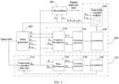
- FIG. 1 a block diagram of a clock data recovery circuit according to an embodiment of the present application is shown.
- a first aspect embodiment of the present application provides a clock data recovery circuit, including a time delay loop 100, a frequency locking loop 200 and a deserializer 300.
- the time delay loop 100 is configured to delay input data according to a phase of a clock signal to realize phase alignment.
- the frequency locking loop 200 is connected to the time delay loop 100, and is configured to adjust a frequency of the clock signal according to the delayed input data to make the frequency of the clock signal be consistent with a frequency of the input data.
- the deserializer 300 is respectively connected to the time delay loop 100 and the frequency locking loop 200, and is configured to deserialize the input data according to the clock signal.
- phase integral factor factor of phase integral
- the frequency locking loop 200 adjusts the frequency of the clock signal based on the phase difference generated due to the mismatch between the frequency of the delayed input data and the frequency of the clock signal, thereby achieving the object of frequency locking.
- the clock signal goes through the deserializer 300 to deserialize the input data.
- introduction of a phase integral factor can be avoided throughout the circuit system, an absolute stable system with merely a single pole can be obtained, and the circuit structure can be simplified.
- the time delay loop 100 includes a numerically controlled delay unit 110, a phase discriminator 120, a first downconverter 130 and a first accumulator 140 connected in sequence. An output of the first accumulator 140 is connected to the numerically controlled delay unit 110.
- the phase discriminator 120 is configured to perform a phase comparison between the clock signal and the input data.
- the numerically controlled delay unit 110 is configured to delay the input data according to a result of the phase comparison, and an output of the numerically controlled delay unit 110 is further connected to the deserializer 300 to output the delayed input data.
- the input data is transmitted from an input of the numerically controlled delay unit 110 to the time delay loop 100, which performs a phase comparison between the clock signal and the delayed input signal through the phase discriminator 120, so that the time delay in the numerically controlled delay unit 110 offsets an injection locking control logic delay.
- the frequency locking loop 200 includes a frequency discriminator 210, a second downconverter 220, a second accumulator 230 and a numerically controlled oscillator 240 connected in sequence.
- the numerically controlled oscillator 240 outputs a clock signal to the phase discriminator 120, the frequency discriminator 210 and the deserializer 300, respectively.
- the output of the numerically controlled delay unit 110 is further connected to the frequency discriminator 210to output the delayed input data.
- the frequency locking loop 200 starts to operate normally when the time delay loop 100 is locked.
- the phases are locked, the phase of the clock signal after injection locking is consistent with the phase of the delayed input data.
- a certain phase difference will be generated due to the mismatch between the frequency of the clock signal and the frequency of the input data, which mismatch can be determined by the frequency discriminator 210, and be input into the second accumulator 230 through the second downconverter 220, thereby controlling an output frequency of the numerically controlled oscillator 240, and achieving the object of frequency locking.
- the clock signal goes through the deserializer to deserialize the data and output half-rate data.
- the clock data recovery circuit further includes a pulse generator 400 having an output connected to the numerically controlled oscillator 240 to output a phase nulling pulse.
- the numerically controlled oscillator 240 performs phase nulling on the output clock signal according to the received phase nulling pulse.
- phase locking is achieved through phase nulling (or called phase zero-setting), wherein certain control logic is used to generate a pulse signal to perform phase nulling on the clock signal output from the numerically controlled oscillator 240.
- phase nulling or called phase zero-setting
- certain control logic is used to generate a pulse signal to perform phase nulling on the clock signal output from the numerically controlled oscillator 240.
- the pulse generator 400 is provided with an input configured to receive input data, so as to generate the phase nulling pulse according to a rising edge of the input data.
- the pulse generator 400 after receiving the input data, the pulse generator 400 generates the phase nulling pulse according to a rising edge of the input data, so as to perform phase nulling on the clock signal output from the numerically controlled oscillator 240. It will be appreciated that the pulse generator 400 generates phase nulling pulses at intervals, for example, every tens of cycles.
- the pulse generator 400 is connected to the phase discriminator 120 to trigger the phase discriminator 120 to perform a phase comparison between the clock signal and the input data.
- the pulse generator 400 in addition to being connected to the numerically controlled oscillator 240, the pulse generator 400 is further connected to the phase discriminator 120. After outputting a phase nulling pulse to the numerically controlled oscillator 240, the pulse generator 400 further outputs a trigger signal to the phase discriminator 120 to trigger the phase discriminator 120 to perform phase comparison between the clock signal and the input data. After passing through the first downconverter 130 and the first accumulator 140, the input data is delayed by the numerically controlled delay unit 110 based on the phase difference between the clock signal and the input data, so as to realize phase alignment of the input data and the clock signal.
- the pulse generator 400 is connected to the frequency discriminator 210 to trigger the frequency discriminator 210 to determine frequencies of the clock signal and the delayed input data.
- the frequency locking loop 200 starts to operate when the time delay loop 100 is locked. Therefore, the pulse generator 400 is connected to the frequency discriminator 210 to output a trigger signal to the frequency discriminator 210, so that the discriminator 210 determines frequencies of the clock signal and the delayed input data after the phase locking. It will be appreciated that the frequency discriminator 210 may also determine the frequencies of the clock signal and the input data before the phase locking, i.e., determine frequencies of the clock signal and the input data not delayed. However, the result of the frequency determination is not accurate due to lack of injection locking of the clock signal.
- phase alignment is achieved by phase nulling, wherein a certain control logic is used to generate a pulse signal to perform phase nulling on the clock output from the numerically controlled oscillator.
- a frequency determination is performed, so as to reduce one phase integral factor. Therefore, an absolute stable system with merely a single pole can be obtained, and thus, an absolute stable system is provided for simplifying the circuit structure.
- an embodiment of the present application further provides a clock data recovery method applied to the clock data recovery circuit as shown in FIG. 1 .
- the clock data recovery circuit includes a time delay loop 100, a frequency locking loop 200 and a deserializer 300.
- the time delay loop 100 is connected to the frequency locking loop 200.
- the deserializer 300 is respectively connected to the time delay loop 100 and the frequency locking loop 200.
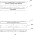
- the clock data recovery method includes the following operations S610 to S630.
- phases of the clock signal and the input data are firstly compared to by the time delay loop 100, so that the input data is delayed to realize phase alignment of the input data and the clock signal, thus introduction of a phase integral factor is avoided.
- the phases are aligned, the phase of the clock signal is consistent with the phase of the delayed input data. If the frequency of the delayed input data is not matched with the frequency of the clock signal, a certain phase difference will be generated after a period of time.
- the frequency locking loop 200 adjusts the frequency of the clock signal based on the phase difference generated due to the mismatch between the frequency of the delayed input data and the frequency of the clock signal, thereby achieving the object of frequency locking.
- the clock signal goes through the deserializer 300 to deserialize the input data.
- introduction of a phase integral factor can be avoided throughout the circuit system, an absolute stable system with merely a single pole can be obtained, and the circuit structure can be simplified.
- the time delay loop 100 includes a numerically controlled delay unit 110, a phase discriminator 120, a first downconverter 130 and a first accumulator 140 connected in sequence.
- An output of the first accumulator 140 is connected to the numerically controlled delay unit 110, and an output of the numerically controlled delay unit 110 is connected to the deserializer 300.
- the operation S610 of delaying, by the time delay loop 100, input data according to the phase of the clock signal to realize phase alignment includes the following operations S710 to S720.
- the input data is transmitted from an input of the numerically controlled delay unit 110 to the time delay loop 100, which performs a phase comparison between the clock signal and the delayed input signal through the phase discriminator 120.
- the numerically controlled delay unit 110 delays the input data according to a result of the phase comparison to realize phase alignment, so that the time delay in the numerically controlled delay unit 110 offsets an injection locking control logic delay.
- the frequency locking loop 200 includes a frequency discriminator 210, a second downconverter 220, a second accumulator 230 and a numerically controlled oscillator 240 connected in sequence.
- the numerically controlled oscillator 240 is connected to the phase discriminator 120, the frequency discriminator 210 and the deserializer 300, respectively.
- the output of the numerically controlled delay unit 110 is further connected to the frequency discriminator 210.
- the operation S620 of adjusting, by the frequency locking loop 200, the frequency of the clock signal according to the delayed input data to make the frequency of the clock signal be consistent with the frequency of the input data includes the following operations S810 to S830.
- the frequency locking loop 200 starts to operate normally when the time delay loop 100 is locked, and thus, the numerically controlled delay unit 110 outputs the delayed input data to the frequency discriminator 210.
- the phases are locked, the phase of the clock signal after injection locking is consistent with the phase of the delayed input data.
- a certain phase difference will be generated due to the mismatch between the frequency of the clock signal and the frequency of the input data, which mismatch can be determined by the frequency discriminator 210, and be input into the second accumulator 230 through the second downconverter 220, thereby controlling an output frequency of the numerically controlled oscillator 240, and achieving the object of frequency locking.
- the clock signal goes through the deserializer to deserialize the data and output half-rate data.
- the clock data recovery circuit includes one time delay loop 100, one frequency locking loop 200, one deserializer 300 and a pulse generator 400.
- the time delay loop 100 includes a numerically controlled delay unit 110, a phase discriminator 120, a first downconverter 130 and a first accumulator 140 connected in sequence.
- An output of the first accumulator 140 is connected to the numerically controlled delay unit 110.
- the frequency locking loop 200 includes a frequency discriminator 210, a second downconverter 220, a second accumulator 230 and a numerically controlled oscillator 240 connected in sequence.
- the numerically controlled oscillator 240 outputs a clock signal to the phase discriminator 120, the frequency discriminator 210 and the deserializer 300, respectively.
- An output of the numerically controlled delay unit 110 is further connected to the frequency discriminator 210 and the deserializer 300.
- An output of the pulse generator 400 is connected to the numerically controlled oscillator 240 to output a phase nulling pulse.
- the time delay loop 100 performs a phase comparison between a clock signal P 0 and the delayed input data D DLY through the phase discriminator 120, so that the time delay in the numerically controlled delay unit 110 offsets an injection locking control logic delay.
- the frequency locking loop 200 starts to operate normally when the time delay loop 100 locks the phases.
- the phase of the clock signal P 0 after injection locking is consistent with the phase of the input data D DLY .
- a certain phase difference will be generated due to the mismatch between the frequency of the clock signal P 0 and the frequency of the input data D DLY , which mismatch can be determined by the frequency discriminator 210, and be input into the digital accumulator (second accumulator) 230 through the 1/16 downconverter (second downconverter) 220, thereby controlling an output frequency of the numerically controlled oscillator 240, and achieving the object of frequency locking.
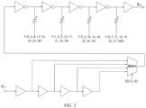
- FIG. 2 is a schematic circuit diagram of the numerically controlled delay unit 110.
- the numerically controlled delay unit 110 performs coarse tuning by selecting different signals with a 2-bit binary code, and performs fine tuning with a 31-bit thermometer code.
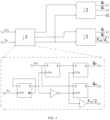
- FIG. 3 is a schematic circuit diagram of the 1/4 downconverter 130. Since the clock data recovery circuit typically has a relatively high frequency, data obtained by the frequency discriminator or the phase discriminator also has a relatively higher frequency, making it impossible to directly enter the accumulator for processing. Therefore, the data is firstly processed by the downconverter before entering the accumulator.
- the working principle of the downconverter is: splitting a single data piece and clock information into two data pieces, while reducing the clock frequency to a half.
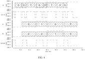
- FIG. 4 is a timing diagram illustrating operation of the 1/4 downconverter circuit.
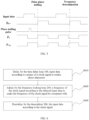
- FIG. 5 is a timing diagram of phase nulling and frequency determination according to an embodiment of the present application.
- the delayed input data D DLY is consistent with the clock signal P 0 in phase, and rising edges of the two are aligned.
- a phase difference will be generated after a period of time due to inconsistent frequencies of the data and the clock, and frequency determination may be performed based on information of the phase difference.
- the frequency determination result shown in FIG. 5 indicates that the frequency of the clock signal is too high. Therefore, the output determination result will be used to reduce an output frequency of the numerically controlled oscillator 240.
- the embodiments of the present application include: a clock data recovery circuit and a clock data recovery method.
- the clock data recovery circuit includes a time delay loop, a frequency locking loop and a deserializer.
- the time delay loop is configured to delay input data according to a phase of a clock signal to realize phase alignment.
- the frequency locking loop is connected to the time delay loop, and is configured to adjust a frequency of the clock signal according to the delayed input data to make the frequency of the clock signal be consistent with a frequency of the input data.
- the deserializer is respectively connected to the time delay loop and the frequency locking loop, and is configured to deserialize the input data according to the clock signal.
- phases of the clock signal and the input data are firstly compared to delay the input data, so as to realize phase alignment of the input data and the clock signal, thus introduction of a phase integral factor is avoided.
- the phases are aligned, the phase of the clock signal is consistent with the phase of the delayed input data. If the frequency of the delayed input data is not matched with the frequency of the clock signal, a certain phase difference will be generated after a period of time.
- the frequency locking loop can adjust the frequency of the clock signal based on the phase difference generated due to the mismatch between the frequency of the delayed input data and the frequency of the clock signal, thereby achieving the object of frequency locking.
- the clock signal goes through the deserializer to deserialize the input data.
- introduction of a phase integral factor can be avoided throughout the circuit system, an absolute stable system with merely a single pole can be obtained, and the circuit structure can be simplified.
Landscapes
- Engineering & Computer Science (AREA)
- Computer Networks & Wireless Communication (AREA)
- Signal Processing (AREA)
- Microelectronics & Electronic Packaging (AREA)
- Synchronisation In Digital Transmission Systems (AREA)
- Stabilization Of Oscillater, Synchronisation, Frequency Synthesizers (AREA)
Abstract
Description
- The present application is based on and claims a priority of the
Chinese patent application No. 202110224295.0 filed on March 1, 2021 - The present application relates to the field of communications, and particularly relates to a clock data recovery circuit and a clock data recovery method.
- In some technical solutions, a phase locking loop in the clock data recovery circuit realizes frequency and phase locking by negative feedback between a phase discriminator, a charge pump, a loop filter, and a voltage controlled oscillator. It has been found in small signal model analysis that a small signal equation Kvco/s of the voltage controlled oscillator is an integral unit, phase accumulations are performed constantly during the process of phase locking, the filter has a capacitance of 1/sC, and charges are accumulated during the charging and discharging processes. Therefore, there are two poles in the closed-loop simulation. In a system with two poles, a phase margin, a gain margin or other stability-related factors of the system must be considered in design of the circuit. Therefore, in some technical solutions, a high-order filter for compensation is necessary in the phase locking loop to ensure stability of the system. Meanwhile, in some technical solutions, the clock data recovery circuit further includes a frequency locking loop for realizing frequency locking. The frequency locking loop and the phase locking loop must work cooperatively, resulting in a complex circuit structure of the clock data recovery circuit.
- Embodiments of the present application provide a clock data recovery circuit and a clock data recovery method.
- In a first aspect, an embodiment of the present application provides a clock data recovery circuit, including a time delay loop, a frequency locking loop and a deserializer, wherein the time delay loop is configured to delay input data according to a phase of a clock signal to realize phase alignment; the frequency locking loop is connected to the time delay loop, and is configured to adjust a frequency of the clock signal according to the delayed input data to make the frequency of the clock signal be consistent with a frequency of the input data; and the deserializer is respectively connected to the time delay loop and the frequency locking loop, and is configured to deserialize the input data according to the clock signal.
- In a second aspect, an embodiment of the present application provides a clock data recovery method applied to a clock data recovery circuit, the clock data recovery circuit including a time delay loop, a frequency locking loop and a deserializer, wherein the time delay loop is connected to the frequency locking loop, and the deserializer is respectively connected to the time delay loop and the frequency locking loop, and the method includes: delaying, by the time delay loop, input data according to a phase of a clock signal to realize phase alignment; adjusting, by the frequency locking loop, a frequency of the clock signal according to the delayed input data to make the frequency of the clock signal be consistent with a frequency of the input data; and deserializing, by the deserializer, the input data according to the clock signal.
- Other features and advantages of the present application will be set forth in the description which follows, and will become apparent from the description at least partially, or be understood by implementing the present application. Objects and other advantages of the present application may be realized and obtained by means of the structures specified in the description, appended claims and drawings.
- Accompanying drawings are provided for further understanding of the technical solution of the present application and constitute a part of the specification. Hereinafter, these drawings are intended to explain the technical solution of the present application together with the following embodiments, but should not be considered as a limitation to the technical solution of the present application.
- The present application is further described below with reference to the accompanying drawings and embodiments;
-
FIG. 1 is a block diagram of a clock data recovery circuit according to an embodiment of the present application; -
FIG. 2 is a circuit diagram of a numerically controlled delay unit of a clock data recovery circuit according to an embodiment of the present application; -
FIG. 3 is a circuit diagram of an 1/4 downconverter according to an embodiment of the present application; -
FIG. 4 is a timing diagram illustrating operation of a 1/4 downconverter circuit according to an embodiment of the present application; -
FIG. 5 is a timing diagram of phase nulling and frequency determination according to an embodiment of the present application; -
FIG. 6 is a flowchart of a clock data recovery method according to an embodiment of the present application; -
FIG. 7 is a flowchart of a clock data recovery method according to another embodiment of the present application; and -
FIG. 8 is a flowchart of a clock data recovery method according to yet another embodiment of the present application. - Specific embodiments of the present application will be described in detail below, where some embodiments of the present application are illustrated in the accompanying drawings which are intended to graphically supplement the description in the text of the specification, so that a person can visually and vividly understand each and every technical feature and the whole technical solution of the present application, but the drawings should not be interpreted as limiting the scope of the present application.
- In the description of the present application, should there be any reference to "first" and "second", it is merely intended to distinguish technical features, instead of being interpreted as indicating or implying any relative importance or implying any number of the indicated technical features or implying any precedence of the indicated technical features.
- In the description of the present application, unless otherwise explicitly defined, terms such as "configure", "install", "connect" and the like should be understood broadly, and those skilled in the art can reasonably determine the specific meanings of the above terms in the present application in combination with specific contents of the technical solutions.
- Embodiments of the present application provide a clock data recovery circuit and a clock data recovery method, which can simplify the circuit structure.
- The embodiments of the present application will be further explained below with reference to the drawings.
- In
FIG. 1 , a block diagram of a clock data recovery circuit according to an embodiment of the present application is shown. - As shown in
FIG. 1 , a first aspect embodiment of the present application provides a clock data recovery circuit, including atime delay loop 100, afrequency locking loop 200 and adeserializer 300. Thetime delay loop 100 is configured to delay input data according to a phase of a clock signal to realize phase alignment. Thefrequency locking loop 200 is connected to thetime delay loop 100, and is configured to adjust a frequency of the clock signal according to the delayed input data to make the frequency of the clock signal be consistent with a frequency of the input data. Thedeserializer 300 is respectively connected to thetime delay loop 100 and thefrequency locking loop 200, and is configured to deserialize the input data according to the clock signal. - According to the clock data recovery circuit of this embodiment, phases of the clock signal and the input data are firstly compared to delay the input data, so as to realize phase alignment of the input data and the clock signal, thus introduction of a phase integral factor (factor of phase integral) is avoid. When the phases are aligned, the phase of the clock signal is consistent with the phase of the delayed input data. If the frequency of the delayed input data is not matched with the frequency of the clock signal, a certain phase difference will be generated after a period of time. The
frequency locking loop 200 adjusts the frequency of the clock signal based on the phase difference generated due to the mismatch between the frequency of the delayed input data and the frequency of the clock signal, thereby achieving the object of frequency locking. When the frequencies and phases of both the input data and the clock signal are locked, the clock signal goes through thedeserializer 300 to deserialize the input data. With the solution provided in this embodiment, introduction of a phase integral factor can be avoided throughout the circuit system, an absolute stable system with merely a single pole can be obtained, and the circuit structure can be simplified. - Referring to
FIG. 1 , in an embodiment, thetime delay loop 100 includes a numerically controlleddelay unit 110, aphase discriminator 120, afirst downconverter 130 and afirst accumulator 140 connected in sequence. An output of thefirst accumulator 140 is connected to the numerically controlleddelay unit 110. Thephase discriminator 120 is configured to perform a phase comparison between the clock signal and the input data. The numerically controlleddelay unit 110 is configured to delay the input data according to a result of the phase comparison, and an output of the numerically controlleddelay unit 110 is further connected to thedeserializer 300 to output the delayed input data. - In this embodiment, the input data is transmitted from an input of the numerically controlled
delay unit 110 to thetime delay loop 100, which performs a phase comparison between the clock signal and the delayed input signal through thephase discriminator 120, so that the time delay in the numerically controlleddelay unit 110 offsets an injection locking control logic delay. - Referring to
FIG. 1 , in an embodiment, thefrequency locking loop 200 includes afrequency discriminator 210, asecond downconverter 220, asecond accumulator 230 and a numerically controlledoscillator 240 connected in sequence. The numerically controlledoscillator 240 outputs a clock signal to the phase discriminator 120, thefrequency discriminator 210 and thedeserializer 300, respectively. The output of the numerically controlleddelay unit 110 is further connected to the frequency discriminator 210to output the delayed input data. - In this embodiment, the
frequency locking loop 200 starts to operate normally when thetime delay loop 100 is locked. When the phases are locked, the phase of the clock signal after injection locking is consistent with the phase of the delayed input data. After a period of time, a certain phase difference will be generated due to the mismatch between the frequency of the clock signal and the frequency of the input data, which mismatch can be determined by thefrequency discriminator 210, and be input into thesecond accumulator 230 through thesecond downconverter 220, thereby controlling an output frequency of the numerically controlledoscillator 240, and achieving the object of frequency locking. When the phases and the frequencies are both locked, the clock signal goes through the deserializer to deserialize the data and output half-rate data. - Referring to
FIG. 1 , in an embodiment, the clock data recovery circuit further includes apulse generator 400 having an output connected to the numerically controlledoscillator 240 to output a phase nulling pulse. The numerically controlledoscillator 240 performs phase nulling on the output clock signal according to the received phase nulling pulse. - In this embodiment, phase locking is achieved through phase nulling (or called phase zero-setting), wherein certain control logic is used to generate a pulse signal to perform phase nulling on the clock signal output from the numerically controlled
oscillator 240. In this manner, introduction of a phase integral factor into the numerically controlledoscillator 240 can be avoided, therefore an absolute stable system with merely a single pole can be obtained, and thus, an absolute stable system is provided for simplifying the circuit structure. - Referring to
FIG. 1 , in an embodiment, thepulse generator 400 is provided with an input configured to receive input data, so as to generate the phase nulling pulse according to a rising edge of the input data. - In this embodiment, after receiving the input data, the
pulse generator 400 generates the phase nulling pulse according to a rising edge of the input data, so as to perform phase nulling on the clock signal output from the numerically controlledoscillator 240. It will be appreciated that thepulse generator 400 generates phase nulling pulses at intervals, for example, every tens of cycles. - Referring to
FIG. 1 , in an embodiment, thepulse generator 400 is connected to thephase discriminator 120 to trigger thephase discriminator 120 to perform a phase comparison between the clock signal and the input data. - In this embodiment, in addition to being connected to the numerically controlled
oscillator 240, thepulse generator 400 is further connected to thephase discriminator 120. After outputting a phase nulling pulse to the numerically controlledoscillator 240, thepulse generator 400 further outputs a trigger signal to thephase discriminator 120 to trigger thephase discriminator 120 to perform phase comparison between the clock signal and the input data. After passing through thefirst downconverter 130 and thefirst accumulator 140, the input data is delayed by the numerically controlleddelay unit 110 based on the phase difference between the clock signal and the input data, so as to realize phase alignment of the input data and the clock signal. - Referring to
FIG. 1 , in an embodiment, thepulse generator 400 is connected to thefrequency discriminator 210 to trigger thefrequency discriminator 210 to determine frequencies of the clock signal and the delayed input data. - In this embodiment, the
frequency locking loop 200 starts to operate when thetime delay loop 100 is locked. Therefore, thepulse generator 400 is connected to thefrequency discriminator 210 to output a trigger signal to thefrequency discriminator 210, so that thediscriminator 210 determines frequencies of the clock signal and the delayed input data after the phase locking. It will be appreciated that thefrequency discriminator 210 may also determine the frequencies of the clock signal and the input data before the phase locking, i.e., determine frequencies of the clock signal and the input data not delayed. However, the result of the frequency determination is not accurate due to lack of injection locking of the clock signal. - In the above clock data recovery circuit, phase alignment is achieved by phase nulling, wherein a certain control logic is used to generate a pulse signal to perform phase nulling on the clock output from the numerically controlled oscillator. Within a certain time after the phase nulling, a frequency determination is performed, so as to reduce one phase integral factor. Therefore, an absolute stable system with merely a single pole can be obtained, and thus, an absolute stable system is provided for simplifying the circuit structure.
- Based on the clock data recovery circuit of the above embodiments, various embodiments of a clock data recovery method are presented below.
- Referring to
FIG. 6 , an embodiment of the present application further provides a clock data recovery method applied to the clock data recovery circuit as shown inFIG. 1 . The clock data recovery circuit includes atime delay loop 100, afrequency locking loop 200 and adeserializer 300. Thetime delay loop 100 is connected to thefrequency locking loop 200. Thedeserializer 300 is respectively connected to thetime delay loop 100 and thefrequency locking loop 200. The clock data recovery method includes the following operations S610 to S630. - At operation S610: delaying, by the
time delay loop 100, input data according to a phase of a clock signal to realize phase alignment. - At operation S620: adjusting, by the
frequency locking loop 200, a frequency of the clock signal according to the delayed input data to make the frequency of the clock signal be consistent with a frequency of the input data. - At operation S630: deserializing, by the
deserializer 300, the input data according to the clock signal. - According to the clock data recovery method provided in the embodiment, phases of the clock signal and the input data are firstly compared to by the
time delay loop 100, so that the input data is delayed to realize phase alignment of the input data and the clock signal, thus introduction of a phase integral factor is avoided. When the phases are aligned, the phase of the clock signal is consistent with the phase of the delayed input data. If the frequency of the delayed input data is not matched with the frequency of the clock signal, a certain phase difference will be generated after a period of time. Thefrequency locking loop 200 adjusts the frequency of the clock signal based on the phase difference generated due to the mismatch between the frequency of the delayed input data and the frequency of the clock signal, thereby achieving the object of frequency locking. When the frequencies and phases of both the input data and the clock signal are locked, the clock signal goes through thedeserializer 300 to deserialize the input data. With the solution provided in this embodiment, introduction of a phase integral factor can be avoided throughout the circuit system, an absolute stable system with merely a single pole can be obtained, and the circuit structure can be simplified. - Referring to
FIG. 1 , in an embodiment, thetime delay loop 100 includes a numerically controlleddelay unit 110, aphase discriminator 120, afirst downconverter 130 and afirst accumulator 140 connected in sequence. An output of thefirst accumulator 140 is connected to the numerically controlleddelay unit 110, and an output of the numerically controlleddelay unit 110 is connected to thedeserializer 300. - Referring to
FIG. 7 , the operation S610 of delaying, by thetime delay loop 100, input data according to the phase of the clock signal to realize phase alignment includes the following operations S710 to S720. - At operation S710: performing, by the
phase discriminator 120, a phase comparison between the clock signal and the input data. - At operation S720: delaying, by the numerically controlled
delay unit 110, the input data according to a result of the phase comparison to realize phase alignment. - In this embodiment, the input data is transmitted from an input of the numerically controlled
delay unit 110 to thetime delay loop 100, which performs a phase comparison between the clock signal and the delayed input signal through thephase discriminator 120. The numerically controlleddelay unit 110 delays the input data according to a result of the phase comparison to realize phase alignment, so that the time delay in the numerically controlleddelay unit 110 offsets an injection locking control logic delay. - Referring to
FIG. 1 , in an embodiment, thefrequency locking loop 200 includes afrequency discriminator 210, asecond downconverter 220, asecond accumulator 230 and a numerically controlledoscillator 240 connected in sequence. The numerically controlledoscillator 240 is connected to thephase discriminator 120, thefrequency discriminator 210 and thedeserializer 300, respectively. The output of the numerically controlleddelay unit 110 is further connected to thefrequency discriminator 210. - Referring to
FIG. 8 , the operation S620 of adjusting, by thefrequency locking loop 200, the frequency of the clock signal according to the delayed input data to make the frequency of the clock signal be consistent with the frequency of the input data includes the following operations S810 to S830. - At operation S810: outputting, by the numerically controlled
delay unit 110, the delayed input data to thefrequency discriminator 210. - At operation S820, determining, by the
frequency discriminator 210, frequencies of the clock signal and the delayed input data. - At operation S830: adjusting, by the numerically controlled
oscillator 240, the frequency of the clock signal according to a phase difference obtained by determining the frequencies. - In this embodiment, the
frequency locking loop 200 starts to operate normally when thetime delay loop 100 is locked, and thus, the numerically controlleddelay unit 110 outputs the delayed input data to thefrequency discriminator 210. When the phases are locked, the phase of the clock signal after injection locking is consistent with the phase of the delayed input data. After a period of time, a certain phase difference will be generated due to the mismatch between the frequency of the clock signal and the frequency of the input data, which mismatch can be determined by thefrequency discriminator 210, and be input into thesecond accumulator 230 through thesecond downconverter 220, thereby controlling an output frequency of the numerically controlledoscillator 240, and achieving the object of frequency locking. When the phases and the frequencies are both locked, the clock signal goes through the deserializer to deserialize the data and output half-rate data. - Implementations of the present application are further described below with reference to
FIGs. 1 to 5 . - A clock data recovery circuit provided in a specific embodiment of the present application is shown in
FIG. 1 . The clock data recovery circuit includes onetime delay loop 100, onefrequency locking loop 200, onedeserializer 300 and apulse generator 400. Thetime delay loop 100 includes a numerically controlleddelay unit 110, aphase discriminator 120, afirst downconverter 130 and afirst accumulator 140 connected in sequence. An output of thefirst accumulator 140 is connected to the numerically controlleddelay unit 110. Thefrequency locking loop 200 includes afrequency discriminator 210, asecond downconverter 220, asecond accumulator 230 and a numerically controlledoscillator 240 connected in sequence. The numerically controlledoscillator 240 outputs a clock signal to thephase discriminator 120, thefrequency discriminator 210 and thedeserializer 300, respectively. An output of the numerically controlleddelay unit 110 is further connected to thefrequency discriminator 210 and thedeserializer 300. An output of thepulse generator 400 is connected to the numerically controlledoscillator 240 to output a phase nulling pulse. When the system is locked, data passing through the numerically controlleddelay unit 110 is deserialized and output. Thetime delay loop 100 performs a phase comparison between a clock signal P0 and the delayed input data DDLY through thephase discriminator 120, so that the time delay in the numerically controlleddelay unit 110 offsets an injection locking control logic delay. Thefrequency locking loop 200 starts to operate normally when thetime delay loop 100 locks the phases. When the phases are locked, the phase of the clock signal P0 after injection locking is consistent with the phase of the input data DDLY. After a period of time, a certain phase difference will be generated due to the mismatch between the frequency of the clock signal P0 and the frequency of the input data DDLY, which mismatch can be determined by thefrequency discriminator 210, and be input into the digital accumulator (second accumulator) 230 through the 1/16 downconverter (second downconverter) 220, thereby controlling an output frequency of the numerically controlledoscillator 240, and achieving the object of frequency locking. When the frequencies and the phases are both locked, the clock goes through thedeserializer 300 to deserialize the data and output half-rate data. Phase locking is achieved through phase nulling, and a certain control logic is used to generate a pulse signal to perform phase nulling on the clock signal output from the numerically controlledoscillator 240. In this manner, introduction of a phase integral factor into the numerically controlled oscillator can be avoided, an absolute stable system with merely a single pole can be obtained, and thus, an absolute stable system is provided for simplifying the circuit structure.FIG. 2 is a schematic circuit diagram of the numerically controlleddelay unit 110. The numerically controlleddelay unit 110 performs coarse tuning by selecting different signals with a 2-bit binary code, and performs fine tuning with a 31-bit thermometer code. Control bits of the thermometer code are uniformly distributed under four loads so that a difference in magnitude of load capacitors is minimized when the thermometer code is changed, thereby avoiding an influence on the duty cycle of signals.FIG. 3 is a schematic circuit diagram of the 1/4downconverter 130. Since the clock data recovery circuit typically has a relatively high frequency, data obtained by the frequency discriminator or the phase discriminator also has a relatively higher frequency, making it impossible to directly enter the accumulator for processing. Therefore, the data is firstly processed by the downconverter before entering the accumulator. The working principle of the downconverter is: splitting a single data piece and clock information into two data pieces, while reducing the clock frequency to a half.FIG. 4 is a timing diagram illustrating operation of the 1/4 downconverter circuit.FIG. 5 is a timing diagram of phase nulling and frequency determination according to an embodiment of the present application. When a phase nulling pulse is generated, the delayed input data DDLY is consistent with the clock signal P0 in phase, and rising edges of the two are aligned. When the phases are consistent, a phase difference will be generated after a period of time due to inconsistent frequencies of the data and the clock, and frequency determination may be performed based on information of the phase difference. The frequency determination result shown inFIG. 5 indicates that the frequency of the clock signal is too high. Therefore, the output determination result will be used to reduce an output frequency of the numerically controlledoscillator 240. - The embodiments of the present application include: a clock data recovery circuit and a clock data recovery method. The clock data recovery circuit includes a time delay loop, a frequency locking loop and a deserializer. The time delay loop is configured to delay input data according to a phase of a clock signal to realize phase alignment. The frequency locking loop is connected to the time delay loop, and is configured to adjust a frequency of the clock signal according to the delayed input data to make the frequency of the clock signal be consistent with a frequency of the input data. The deserializer is respectively connected to the time delay loop and the frequency locking loop, and is configured to deserialize the input data according to the clock signal. According to the solution provided in the embodiments of the present application, phases of the clock signal and the input data are firstly compared to delay the input data, so as to realize phase alignment of the input data and the clock signal, thus introduction of a phase integral factor is avoided. When the phases are aligned, the phase of the clock signal is consistent with the phase of the delayed input data. If the frequency of the delayed input data is not matched with the frequency of the clock signal, a certain phase difference will be generated after a period of time. The frequency locking loop can adjust the frequency of the clock signal based on the phase difference generated due to the mismatch between the frequency of the delayed input data and the frequency of the clock signal, thereby achieving the object of frequency locking. When the frequencies and phases of both the input data and the clock signal are locked, the clock signal goes through the deserializer to deserialize the input data. With the solution provided in this embodiment, introduction of a phase integral factor can be avoided throughout the circuit system, an absolute stable system with merely a single pole can be obtained, and the circuit structure can be simplified.
- The embodiments of the present application have been described in detail with reference to the drawings, but the present application is not limited to the above embodiments, and various changes can be made within the knowledge of those skilled in the art without departing from the scope of the present application.
Claims (10)
- A clock data recovery circuit, comprising:a time delay loop configured to delay input data according to a phase of a clock signal to realize phase alignment;a frequency locking loop connected to the time delay loop and configured to adjust a frequency of the clock signal according to the delayed input data to make the frequency of the clock signal be consistent with a frequency of the input data; anda deserializer respectively connected to the time delay loop and the frequency locking loop and configured to deserialize the input data according to the clock signal.
- The clock data recovery circuit according to claim 1, wherein the time delay loop comprises a numerically controlled delay unit, a phase discriminator, a first downconverter and a first accumulator connected in sequence, wherein an output of the first accumulator is connected to the numerically controlled delay unit, the phase discriminator is configured to perform a phase comparison between the clock signal and the input data, the numerically controlled delay unit is configured to delay the input data according to a result of the phase comparison, and an output of the numerically controlled delay unit is further connected to the deserializer to output the delayed input data.
- The clock data recovery circuit according to claim 2, wherein the frequency locking loop comprises a frequency discriminator, a second downconverter, a second accumulator and a numerically controlled oscillator connected in sequence, wherein the numerically controlled oscillator outputs a clock signal to the phase discriminator, the frequency discriminator and the deserializer, respectively, and wherein the output of the numerically controlled delay unit is further connected to the frequency discriminator to output the delayed input data.
- The clock data recovery circuit according to claim 3, further comprising a pulse generator having an output connected to the numerically controlled oscillator to output a phase nulling pulse, wherein the numerically controlled oscillator performs phase nulling on the output clock signal according to the received phase nulling pulse.
- The clock data recovery circuit according to claim 4, wherein the pulse generator is provided with an input configured to receive input data, so as to generate the phase nulling pulse according to a rising edge of the input data.
- The clock data recovery circuit according to claim 4, wherein the pulse generator is connected to the phase discriminator to trigger the phase discriminator to perform a phase comparison between the clock signal and the input data.
- The clock data recovery circuit according to claim 4, wherein the pulse generator is connected to the frequency discriminator to trigger the frequency discriminator to determine frequencies of the clock signal and the delayed input data.
- A clock data recovery method applied to a clock data recovery circuit, the clock data recovery circuit comprising a time delay loop, a frequency locking loop and a deserializer, wherein the time delay loop is connected to the frequency locking loop, and the deserializer is respectively connected to the time delay loop and the frequency locking loop, and wherein the method comprises:delaying, by the time delay loop, input data according to a phase of a clock signal to realize phase alignment;adjusting, by the frequency locking loop, a frequency of the clock signal according to the delayed input data to make the frequency of the clock signal be consistent with a frequency of the input data; anddeserializing, by the deserializer, the input data according to the clock signal.
- The clock data recovery method according to claim 8, wherein the time delay loop comprises a numerically controlled delay unit, a phase discriminator, a first downconverter and a first accumulator connected in sequence, wherein an output of the first accumulator is connected to the numerically controlled delay unit, and an output of the numerically controlled delay unit is connected to the deserializer; and
wherein the delaying, by the time delay loop, input data according to the phase of the clock signal to realize phase alignment comprises:performing, by the phase discriminator, a phase comparison between the clock signal and the input data; anddelaying, by the numerically controlled delay unit, the input data according to a result of the phase comparison to realize phase alignment. - The clock data recovery method according to claim 9, wherein the frequency locking loop comprises a frequency discriminator, a second downconverter, a second accumulator and a numerically controlled oscillator connected in sequence, wherein the numerically controlled oscillator is connected to the phase discriminator, the frequency discriminator and the deserializer, respectively, and wherein the output of the numerically controlled delay unit is further connected to the frequency discriminator; and
wherein the adjusting, by the frequency locking loop, the frequency of the clock signal according to the delayed input data to make the frequency of the clock signal be consistent with the frequency of the input data comprises:outputting, by the numerically controlled delay unit, the delayed input data to the frequency discriminator;determining, by the frequency discriminator, frequencies of the clock signal and the delayed input data; andadjusting, by the numerically controlled oscillator, the frequency of the clock signal according to a phase difference obtained by determining the frequencies.
Applications Claiming Priority (2)
| Application Number | Priority Date | Filing Date | Title |
|---|---|---|---|
| CN202110224295.0A CN115001486A (en) | 2021-03-01 | 2021-03-01 | Clock data recovery circuit and clock data recovery method |
| PCT/CN2021/130752 WO2022183774A1 (en) | 2021-03-01 | 2021-11-15 | Clock data recovery circuit and clock data recovery method |
Publications (2)
| Publication Number | Publication Date |
|---|---|
| EP4300828A1 true EP4300828A1 (en) | 2024-01-03 |
| EP4300828A4 EP4300828A4 (en) | 2024-08-28 |
Family
ID=83018548
Family Applications (1)
| Application Number | Title | Priority Date | Filing Date |
|---|---|---|---|
| EP21928846.1A Pending EP4300828A4 (en) | 2021-03-01 | 2021-11-15 | CLOCK DATA RECOVERY CIRCUIT AND CLOCK DATA RECOVERY METHOD |
Country Status (5)
| Country | Link |
|---|---|
| US (1) | US12316730B2 (en) |
| EP (1) | EP4300828A4 (en) |
| JP (1) | JP7606632B2 (en) |
| CN (1) | CN115001486A (en) |
| WO (1) | WO2022183774A1 (en) |
Families Citing this family (4)
| Publication number | Priority date | Publication date | Assignee | Title |
|---|---|---|---|---|
| CN115940890A (en) * | 2022-12-30 | 2023-04-07 | 成都市汉云星河网络系统有限公司 | Device and method for recovering clock and data of E1 interface line signal |
| CN117559992B (en) * | 2024-01-12 | 2024-03-19 | 成都电科星拓科技有限公司 | Clock data recovery circuit and chip |
| US12524039B2 (en) * | 2024-03-13 | 2026-01-13 | Avago Technologies International Sales Pte. Limited | Clock calibration for high-speed serial-link transmitters |
| CN119945856B (en) * | 2024-09-27 | 2025-09-26 | 电子科技大学 | A pure analog adaptive real time delay alignment device based on quantization |
Family Cites Families (16)
| Publication number | Priority date | Publication date | Assignee | Title |
|---|---|---|---|---|
| US5036298A (en) | 1990-04-26 | 1991-07-30 | Analog Devices, Inc. | Clock recovery circuit without jitter peaking |
| JP3931477B2 (en) * | 1998-12-03 | 2007-06-13 | 三菱電機株式会社 | Clock regeneration / identification device |
| KR100400043B1 (en) * | 2001-06-11 | 2003-09-29 | 삼성전자주식회사 | Data recovery circuit and method thereof |
| US6747518B1 (en) * | 2002-12-30 | 2004-06-08 | Broadcom Corporation | CDR lock detector with hysteresis |
| EP1619819A4 (en) * | 2003-05-01 | 2010-08-04 | Mitsubishi Electric Corp | CLOCK DATA RECOVERY SYSTEM |
| KR101120711B1 (en) * | 2007-03-20 | 2012-03-26 | 가부시키가이샤 어드밴티스트 | Clock data recovery circuit, method and test device utilizing them |
| KR100889337B1 (en) * | 2007-06-27 | 2009-03-18 | 주식회사 하이닉스반도체 | Clock data recovery circuit |
| US8509371B2 (en) * | 2009-09-29 | 2013-08-13 | Analog Devices, Inc. | Continuous-rate clock recovery circuit |
| JP5704988B2 (en) * | 2011-03-28 | 2015-04-22 | 三菱電機株式会社 | Communication device |
| JP6303513B2 (en) * | 2014-01-14 | 2018-04-04 | 富士通株式会社 | Multilane retimer circuit and multilane transmission system |
| JP2016171387A (en) * | 2015-03-11 | 2016-09-23 | 株式会社日立製作所 | Clock data recovery circuit |
| JP6594710B2 (en) * | 2015-08-31 | 2019-10-23 | ルネサスエレクトロニクス株式会社 | Clock data recovery circuit |
| KR102347844B1 (en) * | 2015-09-02 | 2022-01-10 | 에스케이하이닉스 주식회사 | Integrated circuit |
| US10224978B1 (en) * | 2017-08-16 | 2019-03-05 | Taiwan Semiconductor Manufacturing Co., Ltd. | Clock and data recovery circuit |
| CN110635801B (en) * | 2019-10-26 | 2023-02-10 | 复旦大学 | An Injection Locked Clock Multiplier with Suppression of Reference Spurs |
| US11038666B1 (en) * | 2019-12-11 | 2021-06-15 | Qualcomm Incorporated | Open-loop, super fast, half-rate clock and data recovery for next generation C-PHY interfaces |
-
2021
- 2021-03-01 CN CN202110224295.0A patent/CN115001486A/en active Pending
- 2021-11-15 JP JP2023553438A patent/JP7606632B2/en active Active
- 2021-11-15 EP EP21928846.1A patent/EP4300828A4/en active Pending
- 2021-11-15 WO PCT/CN2021/130752 patent/WO2022183774A1/en not_active Ceased
- 2021-11-15 US US18/279,895 patent/US12316730B2/en active Active
Also Published As
| Publication number | Publication date |
|---|---|
| CN115001486A (en) | 2022-09-02 |
| US12316730B2 (en) | 2025-05-27 |
| EP4300828A4 (en) | 2024-08-28 |
| US20240146502A1 (en) | 2024-05-02 |
| JP2024509432A (en) | 2024-03-01 |
| JP7606632B2 (en) | 2024-12-25 |
| WO2022183774A1 (en) | 2022-09-09 |
Similar Documents
| Publication | Publication Date | Title |
|---|---|---|
| US12316730B2 (en) | Clock data recovery circuit and clock data recovery method | |
| US5789947A (en) | Phase comparator | |
| US7477716B2 (en) | Start up circuit for delay locked loop | |
| US10425086B1 (en) | Divider-less phase locked loop | |
| US10979057B1 (en) | Delay lock loop and phase locking method thereof | |
| US7088155B2 (en) | Clock generating circuit | |
| US11757456B2 (en) | Phase-locked loop circuit and digital operation system | |
| US6915081B2 (en) | PLL circuit and optical communication reception apparatus | |
| US6373308B1 (en) | Direct-measured DLL circuit and method | |
| US4849714A (en) | Signal generating apparatus | |
| EP0731564A2 (en) | Method and apparatus for calculating a divider in a digital phase lock loop | |
| EP0757445A2 (en) | Phase-locked loop frequency synthesizer | |
| US6757349B1 (en) | PLL frequency synthesizer with lock detection circuit | |
| US6501312B1 (en) | Fast-locking DLL circuit and method with phased output clock | |
| US6329847B1 (en) | Radio device including a frequency synthesizer and phase discriminator for such a device | |
| JP2006191372A (en) | Dual loop PLL and multiplying clock generator | |
| US20070201594A1 (en) | Phase Locked Loop (Pll) Circuit, Its Phasing Method And Operation Analyzing Method | |
| CN210469272U (en) | Phase-locked acceleration circuit and phase-locked loop system based on level width extraction | |
| CN101409615A (en) | Receiving system and automatic deviation adjusting method thereof | |
| US6316973B1 (en) | Transmission timing adjusting circuit and method | |
| WO1994026033A1 (en) | Numerically controlled oscillator and digital phase locked loop | |
| EP4686101A1 (en) | Duty cycle calibration circuit, duty cycle calibration method, and clock multiplier circuit | |
| CN114244352A (en) | Clock frequency conversion system, method, processor, chip and electronic equipment | |
| KR20180018257A (en) | Delay locked loop circuit and integrated circuit comprising thereof | |
| EP4686102A1 (en) | Clock duty cycle calibration circuit, method, and clock multiplier circuit |
Legal Events
| Date | Code | Title | Description |
|---|---|---|---|
| STAA | Information on the status of an ep patent application or granted ep patent |
Free format text: STATUS: THE INTERNATIONAL PUBLICATION HAS BEEN MADE |
|
| PUAI | Public reference made under article 153(3) epc to a published international application that has entered the european phase |
Free format text: ORIGINAL CODE: 0009012 |
|
| STAA | Information on the status of an ep patent application or granted ep patent |
Free format text: STATUS: REQUEST FOR EXAMINATION WAS MADE |
|
| 17P | Request for examination filed |
Effective date: 20230927 |
|
| AK | Designated contracting states |
Kind code of ref document: A1 Designated state(s): AL AT BE BG CH CY CZ DE DK EE ES FI FR GB GR HR HU IE IS IT LI LT LU LV MC MK MT NL NO PL PT RO RS SE SI SK SM TR |
|
| DAV | Request for validation of the european patent (deleted) | ||
| DAX | Request for extension of the european patent (deleted) | ||
| REG | Reference to a national code |
Ref country code: DE Ref legal event code: R079 Free format text: PREVIOUS MAIN CLASS: H03L0007180000 Ipc: H03L0007070000 |
|
| A4 | Supplementary search report drawn up and despatched |
Effective date: 20240730 |
|
| RIC1 | Information provided on ipc code assigned before grant |
Ipc: H04J 3/06 20060101ALI20240724BHEP Ipc: H04J 3/04 20060101ALI20240724BHEP Ipc: H04L 7/033 20060101ALI20240724BHEP Ipc: H03L 7/081 20060101ALI20240724BHEP Ipc: H03L 7/093 20060101ALI20240724BHEP Ipc: H03L 7/08 20060101ALI20240724BHEP Ipc: H03L 7/07 20060101AFI20240724BHEP |
|
| RAP3 | Party data changed (applicant data changed or rights of an application transferred) |
Owner name: SOUTHERN UNIVERSITY OF SCIENCE AND TECHNOLOGY Owner name: SANECHIPS TECHNOLOGY CO., LTD. |