EP4300588A1 - Contact architecture for 2d stacked nanoribbon transistor - Google Patents
Contact architecture for 2d stacked nanoribbon transistor Download PDFInfo
- Publication number
- EP4300588A1 EP4300588A1 EP23175335.1A EP23175335A EP4300588A1 EP 4300588 A1 EP4300588 A1 EP 4300588A1 EP 23175335 A EP23175335 A EP 23175335A EP 4300588 A1 EP4300588 A1 EP 4300588A1
- Authority
- EP
- European Patent Office
- Prior art keywords
- channel
- extension
- transistor
- channels
- spacer
- Prior art date
- Legal status (The legal status is an assumption and is not a legal conclusion. Google has not performed a legal analysis and makes no representation as to the accuracy of the status listed.)
- Pending
Links
Images




Classifications
-
- H—ELECTRICITY
- H10—SEMICONDUCTOR DEVICES; ELECTRIC SOLID-STATE DEVICES NOT OTHERWISE PROVIDED FOR
- H10D—INORGANIC ELECTRIC SEMICONDUCTOR DEVICES
- H10D30/00—Field-effect transistors [FET]
- H10D30/40—FETs having zero-dimensional [0D], one-dimensional [1D] or two-dimensional [2D] charge carrier gas channels
- H10D30/47—FETs having zero-dimensional [0D], one-dimensional [1D] or two-dimensional [2D] charge carrier gas channels having two-dimensional [2D] charge carrier gas channels, e.g. nanoribbon FETs or high electron mobility transistors [HEMT]
-
- H—ELECTRICITY
- H10—SEMICONDUCTOR DEVICES; ELECTRIC SOLID-STATE DEVICES NOT OTHERWISE PROVIDED FOR
- H10D—INORGANIC ELECTRIC SEMICONDUCTOR DEVICES
- H10D30/00—Field-effect transistors [FET]
- H10D30/60—Insulated-gate field-effect transistors [IGFET]
- H10D30/67—Thin-film transistors [TFT]
- H10D30/6729—Thin-film transistors [TFT] characterised by the electrodes
- H10D30/673—Thin-film transistors [TFT] characterised by the electrodes characterised by the shapes, relative sizes or dispositions of the gate electrodes
- H10D30/6735—Thin-film transistors [TFT] characterised by the electrodes characterised by the shapes, relative sizes or dispositions of the gate electrodes having gates fully surrounding the channels, e.g. gate-all-around
-
- H—ELECTRICITY
- H10—SEMICONDUCTOR DEVICES; ELECTRIC SOLID-STATE DEVICES NOT OTHERWISE PROVIDED FOR
- H10D—INORGANIC ELECTRIC SEMICONDUCTOR DEVICES
- H10D30/00—Field-effect transistors [FET]
- H10D30/60—Insulated-gate field-effect transistors [IGFET]
- H10D30/67—Thin-film transistors [TFT]
- H10D30/6757—Thin-film transistors [TFT] characterised by the structure of the channel, e.g. transverse or longitudinal shape or doping profile
-
- H—ELECTRICITY
- H10—SEMICONDUCTOR DEVICES; ELECTRIC SOLID-STATE DEVICES NOT OTHERWISE PROVIDED FOR
- H10D—INORGANIC ELECTRIC SEMICONDUCTOR DEVICES
- H10D62/00—Semiconductor bodies, or regions thereof, of devices having potential barriers
- H10D62/10—Shapes, relative sizes or dispositions of the regions of the semiconductor bodies; Shapes of the semiconductor bodies
- H10D62/117—Shapes of semiconductor bodies
- H10D62/118—Nanostructure semiconductor bodies
- H10D62/119—Nanowire, nanosheet or nanotube semiconductor bodies
- H10D62/121—Nanowire, nanosheet or nanotube semiconductor bodies oriented parallel to substrates
-
- H—ELECTRICITY
- H10—SEMICONDUCTOR DEVICES; ELECTRIC SOLID-STATE DEVICES NOT OTHERWISE PROVIDED FOR
- H10D—INORGANIC ELECTRIC SEMICONDUCTOR DEVICES
- H10D62/00—Semiconductor bodies, or regions thereof, of devices having potential barriers
- H10D62/10—Shapes, relative sizes or dispositions of the regions of the semiconductor bodies; Shapes of the semiconductor bodies
- H10D62/13—Semiconductor regions connected to electrodes carrying current to be rectified, amplified or switched, e.g. source or drain regions
- H10D62/149—Source or drain regions of field-effect devices
- H10D62/151—Source or drain regions of field-effect devices of IGFETs
-
- H—ELECTRICITY
- H10—SEMICONDUCTOR DEVICES; ELECTRIC SOLID-STATE DEVICES NOT OTHERWISE PROVIDED FOR
- H10D—INORGANIC ELECTRIC SEMICONDUCTOR DEVICES
- H10D62/00—Semiconductor bodies, or regions thereof, of devices having potential barriers
- H10D62/80—Semiconductor bodies, or regions thereof, of devices having potential barriers characterised by the materials
-
- H—ELECTRICITY
- H10—SEMICONDUCTOR DEVICES; ELECTRIC SOLID-STATE DEVICES NOT OTHERWISE PROVIDED FOR
- H10D—INORGANIC ELECTRIC SEMICONDUCTOR DEVICES
- H10D64/00—Electrodes of devices having potential barriers
- H10D64/20—Electrodes characterised by their shapes, relative sizes or dispositions
- H10D64/23—Electrodes carrying the current to be rectified, amplified, oscillated or switched, e.g. sources, drains, anodes or cathodes
- H10D64/251—Source or drain electrodes for field-effect devices
-
- H—ELECTRICITY
- H10—SEMICONDUCTOR DEVICES; ELECTRIC SOLID-STATE DEVICES NOT OTHERWISE PROVIDED FOR
- H10D—INORGANIC ELECTRIC SEMICONDUCTOR DEVICES
- H10D99/00—Subject matter not provided for in other groups of this subclass
Definitions
- Embodiments of the disclosure are in the field of semiconductor structures and processing and, in particular, to contact architectures for 2D stacked nanoribbon transistors.
- Tri-gate transistors and GAA transistors are generally fabricated on either bulk silicon substrates or silicon-on-insulator substrates. In some instances, bulk silicon substrates are preferred due to their lower cost and compatibility with the existing high-yielding bulk silicon substrate infrastructure.
- Embodiments described herein comprise contact architectures for 2D stacked nanoribbon transistors.
- numerous specific details are set forth, such as specific integration and material regimes, in order to provide a thorough understanding of embodiments of the present disclosure. It will be apparent to one skilled in the art that embodiments of the present disclosure may be practiced without these specific details. In other instances, well-known features, such as integrated circuit design layouts, are not described in detail in order to not unnecessarily obscure embodiments of the present disclosure. Furthermore, it is to be appreciated that the various embodiments shown in the Figures are illustrative representations and are not necessarily drawn to scale.
- Transition metal dichalcogenides enable aggressive scaling of channel length below 10nm. At these channel lengths, the contact resistance is a significant portion of the overall on-resistance.
- One approach to fabricating TMD transistor devices is to grow a metallic phase of the TMD material outside of the spacers.
- metallic phases of TMD materials have higher resistances that traditional bulk contact metal. As such, the number of channels that can be stacked is limited by a high IR drop in the source/drain region.
- a bulk contact metal is deposited outside of the spacers. While the resistance of such a structure is improved, manufacturing functional devices is made more difficult.
- the exposed edge of the TMD channel is narrow (e.g., 1nm or less), and it is difficult to make contact to the TMD channel. That is, opens or voids between the bulk contact metal and the TMD channel may lead to underperforming transistor architectures.
- the transistor device 100 may include a stack of semiconductor channels 120.
- the channels 120 may be a TMD channel material.
- the thickness of the channels 120 may be approximately 1nm or less.
- the channels 120 may have any form factor, such as a nanoribbon form factor or a nanowire form factor.
- a gate stack 140 may be provided around the channels 120.
- the gate stack 140 may include a gate dielectric 142 and a gate metal 141.
- the gate metal 141 may comprise a workfunction metal and a fill metal in some instances.
- the gate stack 140 may be provided around the channels 120 between spacers 132. The ends of the channels 120 may pass through the spacers 132.
- a source/drain region 122 may be provided outside of the spacers 132.
- the source/drain regions 122 may also be a TMD material.
- the source/drain regions 122 may be a metallic phase of the TMD material used for the channels 120.
- the source/drain regions 122 may be grown with an epitaxial growth process. While the epitaxial growth process enables good connection between the source/drain regions 122 and the channels 120, the resistance of the source/drain regions 122 is relatively high. Generally, the resistance is greater than the resistance of a bulk contact metal 125, such as tungsten or the like. Accordingly, as noted above, there is a high IR-drop through the height of the source/drain regions 122.
- the transistor device 100 may include a stack of semiconductor channels 120.
- the channels 120 may be a TMD channel material.
- the thickness of the channels 120 may be approximately 1nm or less.
- the channels 120 may have any form factor, such as a nanoribbon form factor or a nanowire form factor.
- a gate stack 140 may be provided around the channels 120.
- the gate stack 140 may include a gate dielectric 142 and a gate metal 141.
- the gate metal 141 may comprise a workfunction metal and a fill metal in some instances.
- the gate stack 140 may be provided around the channels 120 between spacers 132. The ends of the channels 120 may pass through the spacers 132.
- the source/drain regions include a bulk contact metal 125.
- the use of a bulk contact metal 125 reduces the IR drop through the thickness of the source/drain region. This theoretically will enable the stacking of more channels 120 than the architecture shown in Figure 1A .
- there is a significant drawback to such an architecture Mainly, the contact between the channels 120 and the bulk contact metal 125 is poor. Limitations in etching and deposition processes may result in opens or voids between the ends of the channels 120 and the bulk contact metal 125. This is particularly problematic when the thickness of the channels 120 is reduced below 1nm. Due to the presence of opens or voids, the overall performance of the transistor 100 is diminished.
- embodiments disclosed herein include transistor architectures that allow for both a reduced IR drop and improved electrical coupling at the edge of the semiconductor channels. This is done by forming extensions at the edge of the semiconductor channels.
- the extensions may comprise a metallic phase of the TMD material. Instead of growing the metallic phase of the TMD material to fill the entire source/drain region, small extensions are grown at the outer edges of the semiconductor channels. The remainder of the source/drain region can then be filled with a bulk contact metal that has a lower resistance.
- the extensions also expand the contact surface area, compared to edges of the semiconductor channels. As such, there is more surface area in order to provide improved electrical coupling between the bulk contact metal and the channel. This mitigates or eliminates the formation of opens or voids and results in an improved transistor performance.
- the transistor device 200 is a non-planar transistor device. More particularly, the transistor device 200 may be a GAA device. In an embodiment, the transistor device 200 comprises a stack of semiconductor channels 220. For example, four channels 220 are shown in Figure 2A . Though, it is to be appreciated that any number of channels 220 (e.g., one or more) may be included in the transistor device 200.
- the semiconductor channels 220 may be a TMD semiconductor material.
- TMD materials typically take the form of MX 2 , where M is transition metal atom (e.g., Mo, W, etc.), and X is a chalcogen atom (e.g., S, Se, or Te).
- M transition metal atom
- X a chalcogen atom
- TMD materials may generally be considered a 2D material.
- Other 2D semiconductor materials may also be used in some embodiments disclosed herein.
- the TMD semiconductor material may be a single layer (i.e., a layer of the M atom sandwiched between two X atom layers) or multiple layers thick.
- the channels 220 may have any form factor.
- the channels 220 may include nanoribbon channels 220 or nanowire channels 220.
- a nanoribbon channel refers to a structure that has one confined dimension (e.g., a small thickness compared to a length and a width of the channel), and a nanowire channel refers to a structure that has two confined dimensions (e.g., a small thickness and a small width, compared to a length of the channel).
- the confined dimension may have values of 5nm or smaller, or 1nm or smaller.
- channel lengths may be approximately 10nm or smaller.
- the channels 220 may pass through a pair of spacers 232.
- the ends of the channels 220 may be substantially coplanar with the outer surfaces of the spacers 232.
- the spacers 232 may be any suitable spacer material.
- the spacers 232 may comprise silicon, oxygen, and carbon (e.g., SiOC).
- the spacers 232 may be a material chosen to promote growth of the extensions 250.
- the spacers 232 may comprise aluminum and oxygen (e.g., a-Al 2 O 3 ).
- a gate stack 240 may be provided around the channels 220.
- the gate stack 240 may be positioned between the spacers 232.
- the gate stack 240 may include a gate dielectric 242 and a gate metal 241.
- the gate dielectric 242 may be, for example, any suitable oxide such as silicon dioxide or high-k gate dielectric materials.
- high-k gate dielectric materials include, for instance, hafnium oxide, hafnium silicon oxide, lanthanum oxide, lanthanum aluminum oxide, zirconium oxide, zirconium silicon oxide, tantalum oxide, titanium oxide, barium strontium titanium oxide, barium titanium oxide, strontium titanium oxide, yttrium oxide, aluminum oxide, lead scandium tantalum oxide, and lead zinc niobate.
- an annealing process may be carried out on the gate dielectric 242 to improve its quality when a high-k material is used.
- the gate metal 241 may include a workfunction metal and a fill metal.
- the gate metal 241 preferably has a workfunction that is between about 3.9 eV and about 4.2 eV.
- N-type materials that may be used to form the gate metal 241 include, but are not limited to, hafnium, zirconium, titanium, tantalum, aluminum, and metal carbides that include these elements, i.e., titanium carbide, zirconium carbide, tantalum carbide, hafnium carbide and aluminum carbide.
- the gate metal 241 preferably has a workfunction that is between about 4.9 eV and about 5.2 eV.
- P-type materials that may be used to form the gate metal 241 include, but are not limited to, ruthenium, palladium, platinum, cobalt, nickel, and conductive metal oxides, e.g., ruthenium oxide.
- the transistor 200 may further comprise extensions 250 at the ends of the channels 232.
- the extensions 250 may be in direct contact with the end surfaces of the channels 220 and the outside surfaces of the spacers 232.
- the extensions 250 may be a metal phase of the TMD used to form the channels 220.
- the extensions 250 may be grown over the ends of the channels 220 with an epitaxial growth process. As such, the connection between the extensions 250 and the channels 220 will be excellent without any voids or openings.
- the extensions 250 may have a semicircular cross-section.
- the flat surface of the extensions 250 may contact the channels 220 and the outside surfaces of the spacers 232, and the rounded surface of the extensions 250 may face away from the channels 220.
- a height H of the extensions 250 may be approximately 10nm or smaller. In a particular embodiment, the height H of the extensions 250 may be between approximately 5nm and approximately 10nm.
- "approximately” may refer to a range of values within ten percent of the stated value. For example, approximately 10nm may refer to a range between 9nm and 11nm.
- a width Wi of the extensions 250 may be up to half of the width W 2 of the bulk contact metal 225. For example, the width Wi may be up to approximately 5nm, and the width W 2 may be up to approximately 10nm.
- each of the extensions 250 may be discrete from each other. That is, the spacing between the channels 220 may be large enough in order to grow the extensions to a desired size without the extensions 250 merging together. Keeping the extensions 250 separate from each other increases the total surface area available to be contacted with the bulk contact metal 225. For example, a portion of the bulk contact metal 225 may be provided between neighboring extensions 250. The portion of the bulk contact metal 225 between neighboring extensions 250 may directly contact an outer surface of the spacer 232. As such, the contact resistance can be reduced, and performance may be improved.
- the bulk contact metal 225 may be any suitable contact metal used in semiconductor processing environments.
- the bulk contact metal 225 may comprise tungsten, other metals, or other alloys.
- the bulk contact metal 225 may conform to the shape of the extensions 250.
- the bulk contact metal 225 may be in direct contact with the spacers 232 and the extensions 250. However, due to the presence of the extensions 250, the bulk contact metal 225 may not directly contact the channels 220.
- the transistor device 200 comprises a stack of semiconductor channels 220.
- the channels 220 may comprise a semiconductive TMD material.
- spacers 232 may be provided at the ends of the channels 220.
- a gate stack 240 may be provided around the channels 220 between the spacers 232.
- the gate stack 240 may comprise a gate metal 241 and a gate dielectric 242.
- the materials for the spacers 232, the gate metal 241, and the gate dielectric 242 may be substantially similar to materials for the similarly named structures described above with respect to Figure 2A .
- the transistor 200 may further comprise merged extensions 251 on opposite ends of the channels 220.
- the merged extensions 251 may include a metallic phase of the TMD material used to form the channels 220.
- the merged extensions 251 may be epitaxially grown from the edges of the channels 220. As such, the growth starts with extensions on individual ones of the channels 220. As the growth continues, the discrete extensions begin to merge together in order to form a single merged extension 251 on each side of the channels.
- the merged extension 251 may have a substantially planar surface facing the spacer 232 and the channels 220. The opposite surface of the merged extensions 251 may be non-planar.
- the non-planar surface may be referred to as a scalloped surface in some embodiments.
- the non-planar surface may have ridges 261 that are substantially aligned with (e.g., centered on) the channels 220 and valleys 262 that are provided between the channels 220.
- the transistor device 200 comprises a stack of semiconductor channels 220.
- the channels 220 may comprise a semiconductive TMD material.
- spacers 232 may be provided at the ends of the channels 220.
- a gate stack 240 may be provided around the channels 220 between the spacers 232.
- the gate stack 240 may comprise a gate metal 241 and a gate dielectric 242.
- the materials for the spacers 232, the gate metal 241, and the gate dielectric 242 may be substantially similar to materials for the similarly named structures described above with respect to Figure 2A .
- extensions 250 are provided at the ends of each of the channels 220.
- the extensions 250 may comprise a metallic phase of the TMD material used for the channels 220.
- the extensions 250 are distinct features. That is, the extensions 250 are not merged together in some embodiments.
- the extensions 250 may include a surface treatment 252.
- the surface treatment 252 may be a treatment that decreases the contact resistance between the bulk contact metal 225 and the extensions 250.
- the surface treatment 252 may be similar to the use of a silicide in silicon based devices.
- the surface treatment 252 may include a nitric oxide treatment of the extensions 250.
- the surface treatment 252 may comprise nitrogen.
- the surface treatment 252 may be on surfaces of the extension 250 that are between the extension 250 and the bulk contact metal 225. That is, the surfaces of the extension 250 that face the spacers 232 and the channels 220 may not have the surface treatment 252.
- non-merged extensions 250 are shown in Figure 2C , it is to be appreciated that similar surface treatments 252 may also be applied in a merged architecture, such as the example shown in Figure 2B .
- the surface treatment 252 may be a continuous layer that is formed along the surfaces of the merged extensions 251 that interface with the bulk contact metal 225.
- FIG. 3A-3C a series of illustrations depicting a process for forming a transistor with metallic phase TMD extensions is shown, in accordance with an embodiment.
- a stack of semiconductor channels 320 may pass through a spacer 332.
- the channels 320 may also pass through a gate stack 340 and the spacer 332 on the opposite side of Figure 3A .
- the gate stack 340 may be a dummy gate stack, or the final gate stack. In the case of a dummy gate stack, the gate stack 340 may be replaced with the gate dielectric and gate metal is a subsequent processing operation, as is known in the art of semiconductor fabrication.
- six channels 320 are shown. However, it is to be appreciated that any number of channels 320 may be used in the transistor device 300.
- the channels 320 are shown as being nanoribbon structures. However, in other embodiments, the channels 320 may be nanowire structures.
- the channels 320 may include any suitable semiconductor TMD material. The use of TMD materials allows for aggressive scaling of the transistor device 300. For example, channel lengths of the transistor device may be approximately 10nm or smaller.
- the transistor device 300 may be fabricated over a substrate 301.
- the substrate 301 may include a semiconductor substrate, such as a silicon substrate.
- the semiconductor substrate 301 often includes a wafer or other piece of silicon or another semiconductor material.
- Suitable semiconductor substrates 301 include, but are not limited to, single crystal silicon, polycrystalline silicon and silicon on insulator (SOI), as well as similar substrates formed of other semiconductor materials, such as substrates including germanium, carbon, or group III-V materials.
- the extensions 350 may be a metal phase of the TMD material used for the channels 320.
- the extensions 350 may be grown with an epitaxial process.
- the extensions 350 may be grown with an atomic layer deposition (ALD) process or a chemical vapor deposition (CVD) process.
- the extensions 350 may have rounded surfaces that face away from the spacer 332.
- the growth of the extensions 350 is halted before the individual extensions 350 begin to merge together.
- the extensions 350 may be grown until the extensions 350 begin to merge together (e.g., similar to the embodiment shown in Figure 2B ).
- a surface treatment may be applied to the extensions 350.
- a nitric oxide treatment may be applied to PMOS type contacts.
- the extensions 350 may also comprise nitrogen.
- the bulk contact metal 325 may surround the extensions 350 outside of the spacers 332.
- the bulk contact metal 325 may be deposited with any suitable deposition process. For example, a CVD process may be used in some embodiments. Due to the decreased resistance compared to the extensions 350, the bulk contact metal 325 reduces the IR drop and allows for an increased number of channels 320 to be stacked in the transistor device 300. Additionally, the increased surface area of the extensions 350 allows for improved electrical coupling to the channels 320.
- FIG. 4 illustrates a computing device 400 in accordance with one implementation of an embodiment of the disclosure.
- the computing device 400 houses a board 402.
- the board 402 may include a number of components, including but not limited to a processor 404 and at least one communication chip 406.
- the processor 404 is physically and electrically coupled to the board 402.
- the at least one communication chip 406 is also physically and electrically coupled to the board 402.
- the communication chip 406 is part of the processor 404.
- computing device 400 may include other components that may or may not be physically and electrically coupled to the board 402. These other components include, but are not limited to, volatile memory (e.g., DRAM), nonvolatile memory (e.g., ROM), flash memory, a graphics processor, a digital signal processor, a crypto processor, a chipset, an antenna, a display, a touchscreen display, a touchscreen controller, a battery, an audio codec, a video codec, a power amplifier, a global positioning system (GPS) device, a compass, an accelerometer, a gyroscope, a speaker, a camera, and a mass storage device (such as hard disk drive, compact disk (CD), digital versatile disk (DVD), and so forth).
- volatile memory e.g., DRAM
- nonvolatile memory e.g., ROM
- flash memory e.g., a graphics processor, a digital signal processor, a crypto processor, a chipset, an antenna, a display,
- the communication chip 406 enables wireless communications for the transfer of data to and from the computing device 400.
- wireless and its derivatives may be used to describe circuits, devices, systems, methods, techniques, communications channels, etc., that may communicate data through the use of modulated electromagnetic radiation through a non-solid medium. The term does not imply that the associated devices do not contain any wires, although in some embodiments they might not.
- the communication chip 406 may implement any of a number of wireless standards or protocols, including but not limited to Wi-Fi (IEEE 802.11 family), WiMAX (IEEE 802.16 family), IEEE 802.20, long term evolution (LTE), Ev-DO, HSPA+, HSDPA+, HSUPA+, EDGE, GSM, GPRS, CDMA, TDMA, DECT, Bluetooth, derivatives thereof, as well as any other wireless protocols that are designated as 3G, 4G, 5G, and beyond.
- the computing device 400 may include a plurality of communication chips 406.
- a first communication chip 406 may be dedicated to shorter range wireless communications such as Wi-Fi and Bluetooth and a second communication chip 406 may be dedicated to longer range wireless communications such as GPS, EDGE, GPRS, CDMA, WiMAX, LTE, Ev-DO, and others.
- the processor 404 of the computing device 400 includes an integrated circuit die packaged within the processor 404.
- the integrated circuit die of the processor may comprise a transistor device with a GAA structure that includes extensions out from a TMD channel, as described herein.
- the term "processor" may refer to any device or portion of a device that processes electronic data from registers and/or memory to transform that electronic data into other electronic data that may be stored in registers and/or memory.
- the communication chip 406 also includes an integrated circuit die packaged within the communication chip 406.
- the integrated circuit die of the communication chip may comprise a transistor device with a GAA structure that includes extensions out from a TMD channel, as described herein.
- another component housed within the computing device 400 may comprise a transistor device with a GAA structure that includes extensions out from a TMD channel, as described herein.
- the computing device 400 may be a laptop, a netbook, a notebook, an ultrabook, a smartphone, a tablet, a personal digital assistant (PDA), an ultra mobile PC, a mobile phone, a desktop computer, a server, a printer, a scanner, a monitor, a set-top box, an entertainment control unit, a digital camera, a portable music player, or a digital video recorder.
- the computing device 400 may be any other electronic device that processes data.
- FIG. 5 illustrates an interposer 500 that includes one or more embodiments of the disclosure.
- the interposer 500 is an intervening substrate used to bridge a first substrate 502 to a second substrate 504.
- the first substrate 502 may be, for instance, an integrated circuit die.
- the second substrate 504 may be, for instance, a memory module, a computer motherboard, or another integrated circuit die.
- one of both of the first substrate 502 and the second substrate 504 may comprise a transistor device with a GAA structure that includes extensions out from a TMD channel, in accordance with embodiments described herein.
- the purpose of an interposer 500 is to spread a connection to a wider pitch or to reroute a connection to a different connection.
- an interposer 500 may couple an integrated circuit die to a ball grid array (BGA) 506 that can subsequently be coupled to the second substrate 504.
- BGA ball grid array
- the first and second substrates 502/504 are attached to opposing sides of the interposer 500.
- the first and second substrates 502/504 are attached to the same side of the interposer 500.
- three or more substrates are interconnected by way of the interposer 500.
- the interposer 500 may be formed of an epoxy resin, a fiberglass-reinforced epoxy resin, a ceramic material, or a polymer material such as polyimide. In further implementations, the interposer 500 may be formed of alternate rigid or flexible materials that may include the same materials described above for use in a semiconductor substrate, such as silicon, germanium, and other group III-V and group IV materials.
- the interposer 500 may include metal interconnects 508 and vias 510, including but not limited to through-silicon vias (TSVs) 512.
- the interposer 500 may further include embedded devices 514, including both passive and active devices.
- Such devices include, but are not limited to, capacitors, decoupling capacitors, resistors, inductors, fuses, diodes, transformers, sensors, and electrostatic discharge (ESD) devices.
- More complex devices such as radio-frequency (RF) devices, power amplifiers, power management devices, antennas, arrays, sensors, and MEMS devices may also be formed on the interposer 500.
- apparatuses or processes disclosed herein may be used in the fabrication of interposer 500.
- embodiments of the present disclosure may comprise a transistor device with a GAA structure that includes extensions out from a TMD channel.
- Example 1 a transistor, comprising: a channel with a first end and a second end opposite from the first end; a first spacer around the first end of the channel; a second spacer around the second end of the channel; a gate stack over the channel, wherein the gate stack is between the first spacer and the second spacer; a first extension contacting the first end of the channel; a second extension contacting the first end of the channel; and conductive layers over the first extension and the second extension outside of the first spacer and the second spacer.
- Example 2 the transistor of Example 1, wherein the channel is a nanoribbon channel.
- Example 3 the transistor of Example 1, wherein the channel is a nanowire channel.
- Example 4 the transistor of Example 1 or Example 2, wherein the channel is a transition metal dichalcogenide (TMD).
- TMD transition metal dichalcogenide
- Example 5 the transistor of Example 4, wherein the first extension and the second extension are metallic phase TMDs.
- Example 6 the transistor of Examples 1-5, wherein the first extension and the second extension have semicircular cross-sections.
- Example 7 the transistor of Example 6, wherein portions of the first extension and the second extension contact the first spacer or the second spacer.
- Example 8 the transistor of Examples 1-7, wherein a height of the first extension and the second extension is between approximately 5nm and approximately 10nm.
- Example 9 the transistor of Examples 1-8, wherein a width of the first extension and the second extension is up to approximately half of a width of the conductive layers.
- Example 10 the transistor of Example 9, wherein the width of the first extension and the second extension is approximately 5nm or less.
- Example 11 the transistor of Examples 1-10, further comprising: a surface treatment layer over the first extension and the second extension.
- Example 12 the transistor of Example 11, wherein the surface treatment layer comprises nitrogen.
- Example 13 the transistor of Examples 1-12, wherein the first spacer and the second spacer comprise aluminum and oxygen.
- Example 14 the transistor of Examples 1-13, wherein a channel length of the channel is approximately 10nm or less.
- Example 15 a transistor device, comprising: a stack of semiconductor channels; a gate stack over and around the stack of semiconductor channels; spacers at opposite ends of the gate stack; and extensions at ends of individual ones of the semiconductor channels.
- Example 16 the transistor device of Example 15, wherein the extensions merge together to form a single body.
- Example 17 the transistor device of Example 15 or Example 16, wherein the extensions directly contact semiconductor channels and the spacers.
- Example 18 the transistor device of Examples 15-17, wherein the extensions have a surface treatment layer comprising nitrogen.
- Example 19 the transistor device of Examples 15-18, wherein the stack of semiconductor channels comprise transition metal dichalcogenide (TMD) materials.
- TMD transition metal dichalcogenide
- Example 20 the transistor device of Example 19, wherein the extensions comprise metallic phase TMD materials.
- Example 21 the transistor device of Examples 15-20, further comprising: conductive layers around the extensions.
- Example 22 the transistor device of Example 21, wherein a width of the conductive layers is approximately twice a width of the extensions or greater.
- Example 23 an electronic system, comprising: a board; a package substrate coupled to the board; and a die coupled to the package substrate, wherein the die comprises: a gate-all-around (GAA) transistor device with a semiconductor channel that is surrounded by a gate stack that is between a pair of spacers, wherein extensions are provided at ends of the semiconductor channel outside of the spacers, and wherein the semiconductor channel comprises a transition metal dichalcogenide (TMD), wherein the TMD takes the form of MX 2 , wherein M is transition metal atom including molybdenum or tungsten, and X is a chalcogen atom including sulfur, selenium, or tellurium.
- GAA gate-all-around
- TMD transition metal dichalcogenide
- Example 24 the electronic system of Example 23, wherein the extensions comprise a metallic phase TMD.
- Example 25 the electronic system of Example 23 or Example 24, wherein the extensions contact the semiconductor channel and the spacers, and wherein a conductive layer is provided around the extensions.
Landscapes
- Electrodes Of Semiconductors (AREA)
Abstract
Description
- Embodiments of the disclosure are in the field of semiconductor structures and processing and, in particular, to contact architectures for 2D stacked nanoribbon transistors.
- For the past several decades, the scaling of features in integrated circuits has been a driving force behind an ever-growing semiconductor industry. Scaling to smaller and smaller features enables increased densities of functional units on the limited real estate of semiconductor chips. For example, shrinking transistor size allows for the incorporation of an increased number of memory or logic devices on a chip, lending to the fabrication of products with increased capacity. The drive for ever-more capacity, however, is not without issue. The necessity to optimize the performance of each device becomes increasingly significant.
- Variability in conventional and currently known fabrication processes may limit the possibility to further extend them into the 10 nanometer node or sub-10 nanometer node range. Consequently, fabrication of the functional components needed for future technology nodes may require the introduction of new methodologies or the integration of new technologies in current fabrication processes or in place of current fabrication processes.
- In the manufacture of integrated circuit devices, multi-gate transistors, such as tri-gate transistors and gate-all-around (GAA) transistors, have become more prevalent as device dimensions continue to scale down. Tri-gate transistors and GAA transistors are generally fabricated on either bulk silicon substrates or silicon-on-insulator substrates. In some instances, bulk silicon substrates are preferred due to their lower cost and compatibility with the existing high-yielding bulk silicon substrate infrastructure.
- Scaling multi-gate transistors has not been without consequence, however. As the dimensions of these fundamental building blocks of microelectronic circuitry are reduced and as the sheer number of fundamental building blocks fabricated in a given region is increased, the constraints on the semiconductor processes used to fabricate these building blocks have become overwhelming.
-
-
Figure 1A is a cross-sectional illustration of a transistor device with a gate-all-around (GAA) structure with source/drain regions provided on ends of the semiconductor channels. -
Figure 1B is a cross-sectional illustration of a transistor device with a GAA structure with a contact metal directly contacting the ends of the semiconductor channels. -
Figure 2A is a cross-sectional illustration of a transistor device with a GAA structure that includes conductive extensions at the ends of the semiconductor channels, in accordance with an embodiment. -
Figure 2B is a cross-sectional illustration of a transistor device with a GAA structure that includes conductive extensions at the ends of the semiconductor channels that have merged together, in accordance with an embodiment. -
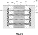
Figure 2C is a cross-sectional illustration of a transistor device with a GAA structure that includes conductive extensions at the ends of the semiconductor channels that include a surface treatment, in accordance with an embodiment. -
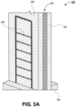
Figure 3A is a perspective view illustration of a transistor device with a gate stack over the semiconductor channels, where the gate stack is between spacers, in accordance with an embodiment. -
Figure 3B is a perspective view illustration of the transistor device after extensions are grown on the ends of the semiconductor channels that pass through the spacers, in accordance with an embodiment. -
Figure 3C is a perspective view illustration of the transistor device after a contact metal is disposed around the extensions outside of the spacers, in accordance with an embodiment. -
Figure 4 illustrates a computing device in accordance with one implementation of an embodiment of the disclosure. -
Figure 5 is an interposer implementing one or more embodiments of the disclosure. - Embodiments described herein comprise contact architectures for 2D stacked nanoribbon transistors. In the following description, numerous specific details are set forth, such as specific integration and material regimes, in order to provide a thorough understanding of embodiments of the present disclosure. It will be apparent to one skilled in the art that embodiments of the present disclosure may be practiced without these specific details. In other instances, well-known features, such as integrated circuit design layouts, are not described in detail in order to not unnecessarily obscure embodiments of the present disclosure. Furthermore, it is to be appreciated that the various embodiments shown in the Figures are illustrative representations and are not necessarily drawn to scale.
- Certain terminology may also be used in the following description for the purpose of reference only, and thus are not intended to be limiting. For example, terms such as "upper", "lower", "above", "below," "bottom," and "top" refer to directions in the drawings to which reference is made. Terms such as "front", "back", "rear", and "side" describe the orientation and/or location of portions of the component within a consistent but arbitrary frame of reference which is made clear by reference to the text and the associated drawings describing the component under discussion. Such terminology may include the words specifically mentioned above, derivatives thereof, and words of similar import.
- Transition metal dichalcogenides (TMDs) enable aggressive scaling of channel length below 10nm. At these channel lengths, the contact resistance is a significant portion of the overall on-resistance. One approach to fabricating TMD transistor devices is to grow a metallic phase of the TMD material outside of the spacers. However, metallic phases of TMD materials have higher resistances that traditional bulk contact metal. As such, the number of channels that can be stacked is limited by a high IR drop in the source/drain region. In an alternative architecture, a bulk contact metal is deposited outside of the spacers. While the resistance of such a structure is improved, manufacturing functional devices is made more difficult. This is because the exposed edge of the TMD channel is narrow (e.g., 1nm or less), and it is difficult to make contact to the TMD channel. That is, opens or voids between the bulk contact metal and the TMD channel may lead to underperforming transistor architectures.
- Referring now to
Figure 1A , a cross-sectional illustration of atransistor device 100 is shown. Thetransistor device 100 may include a stack ofsemiconductor channels 120. Thechannels 120 may be a TMD channel material. The thickness of thechannels 120 may be approximately 1nm or less. Thechannels 120 may have any form factor, such as a nanoribbon form factor or a nanowire form factor. Agate stack 140 may be provided around thechannels 120. For example, thegate stack 140 may include a gate dielectric 142 and agate metal 141. Thegate metal 141 may comprise a workfunction metal and a fill metal in some instances. Thegate stack 140 may be provided around thechannels 120 betweenspacers 132. The ends of thechannels 120 may pass through thespacers 132. - As shown, a source/
drain region 122 may be provided outside of thespacers 132. The source/drain regions 122 may also be a TMD material. For example, the source/drain regions 122 may be a metallic phase of the TMD material used for thechannels 120. The source/drain regions 122 may be grown with an epitaxial growth process. While the epitaxial growth process enables good connection between the source/drain regions 122 and thechannels 120, the resistance of the source/drain regions 122 is relatively high. Generally, the resistance is greater than the resistance of abulk contact metal 125, such as tungsten or the like. Accordingly, as noted above, there is a high IR-drop through the height of the source/drain regions 122. This negatively impacts the functionality of thechannels 120 towards the bottom of the stack. Therefore, the number ofchannels 120 that can be stacked in thetransistor 100 is limited. This negatively impacts scalability of thetransistor 100. Additionally, not all TMD materials have an easy to grow metallic counterpart. This limits the material classes used to form thetransistor 100. - Referring now to
Figure 1B , a cross-sectional illustration of atransistor device 100 is shown in accordance with an alternative architecture. Thetransistor device 100 may include a stack ofsemiconductor channels 120. Thechannels 120 may be a TMD channel material. The thickness of thechannels 120 may be approximately 1nm or less. Thechannels 120 may have any form factor, such as a nanoribbon form factor or a nanowire form factor. Agate stack 140 may be provided around thechannels 120. For example, thegate stack 140 may include agate dielectric 142 and agate metal 141. Thegate metal 141 may comprise a workfunction metal and a fill metal in some instances. Thegate stack 140 may be provided around thechannels 120 betweenspacers 132. The ends of thechannels 120 may pass through thespacers 132. - Instead of having a metallic phase of the TMD material, the source/drain regions include a
bulk contact metal 125. The use of abulk contact metal 125 reduces the IR drop through the thickness of the source/drain region. This theoretically will enable the stacking ofmore channels 120 than the architecture shown inFigure 1A . However, as noted above, there is a significant drawback to such an architecture. Mainly, the contact between thechannels 120 and thebulk contact metal 125 is poor. Limitations in etching and deposition processes may result in opens or voids between the ends of thechannels 120 and thebulk contact metal 125. This is particularly problematic when the thickness of thechannels 120 is reduced below 1nm. Due to the presence of opens or voids, the overall performance of thetransistor 100 is diminished. - Accordingly, embodiments disclosed herein include transistor architectures that allow for both a reduced IR drop and improved electrical coupling at the edge of the semiconductor channels. This is done by forming extensions at the edge of the semiconductor channels. The extensions may comprise a metallic phase of the TMD material. Instead of growing the metallic phase of the TMD material to fill the entire source/drain region, small extensions are grown at the outer edges of the semiconductor channels. The remainder of the source/drain region can then be filled with a bulk contact metal that has a lower resistance. The extensions also expand the contact surface area, compared to edges of the semiconductor channels. As such, there is more surface area in order to provide improved electrical coupling between the bulk contact metal and the channel. This mitigates or eliminates the formation of opens or voids and results in an improved transistor performance.
- Referring now to
Figure 2A , a cross-sectional illustration of atransistor device 200 is shown, in accordance with an embodiment. In an embodiment, thetransistor device 200 is a non-planar transistor device. More particularly, thetransistor device 200 may be a GAA device. In an embodiment, thetransistor device 200 comprises a stack ofsemiconductor channels 220. For example, fourchannels 220 are shown inFigure 2A . Though, it is to be appreciated that any number of channels 220 (e.g., one or more) may be included in thetransistor device 200. - In a particular embodiment, the
semiconductor channels 220 may be a TMD semiconductor material. TMD materials typically take the form of MX2, where M is transition metal atom (e.g., Mo, W, etc.), and X is a chalcogen atom (e.g., S, Se, or Te). Typically, a layer of M atoms are sandwiched between layers of chalcogen atoms. TMD materials may generally be considered a 2D material. Other 2D semiconductor materials may also be used in some embodiments disclosed herein. The TMD semiconductor material may be a single layer (i.e., a layer of the M atom sandwiched between two X atom layers) or multiple layers thick. Thechannels 220 may have any form factor. For example, thechannels 220 may includenanoribbon channels 220 ornanowire channels 220. A nanoribbon channel refers to a structure that has one confined dimension (e.g., a small thickness compared to a length and a width of the channel), and a nanowire channel refers to a structure that has two confined dimensions (e.g., a small thickness and a small width, compared to a length of the channel). In a particular embodiment, the confined dimension (or dimensions) may have values of 5nm or smaller, or 1nm or smaller. The use of TMD semiconductor materials allows for aggressive scaling of thetransistor device 200. For example, channel lengths may be approximately 10nm or smaller. - In an embodiment, the
channels 220 may pass through a pair ofspacers 232. The ends of thechannels 220 may be substantially coplanar with the outer surfaces of thespacers 232. In an embodiment, thespacers 232 may be any suitable spacer material. In one instance thespacers 232 may comprise silicon, oxygen, and carbon (e.g., SiOC). In other embodiments, thespacers 232 may be a material chosen to promote growth of theextensions 250. For example, thespacers 232 may comprise aluminum and oxygen (e.g., a-Al2O3). - In an embodiment, a
gate stack 240 may be provided around thechannels 220. Thegate stack 240 may be positioned between thespacers 232. In an embodiment, thegate stack 240 may include agate dielectric 242 and agate metal 241. Thegate dielectric 242 may be, for example, any suitable oxide such as silicon dioxide or high-k gate dielectric materials. Examples of high-k gate dielectric materials include, for instance, hafnium oxide, hafnium silicon oxide, lanthanum oxide, lanthanum aluminum oxide, zirconium oxide, zirconium silicon oxide, tantalum oxide, titanium oxide, barium strontium titanium oxide, barium titanium oxide, strontium titanium oxide, yttrium oxide, aluminum oxide, lead scandium tantalum oxide, and lead zinc niobate. In some embodiments, an annealing process may be carried out on thegate dielectric 242 to improve its quality when a high-k material is used. - In an embodiment, the
gate metal 241 may include a workfunction metal and a fill metal. When the workfunction metal will serve as an N-type workfunction metal, thegate metal 241 preferably has a workfunction that is between about 3.9 eV and about 4.2 eV. N-type materials that may be used to form thegate metal 241 include, but are not limited to, hafnium, zirconium, titanium, tantalum, aluminum, and metal carbides that include these elements, i.e., titanium carbide, zirconium carbide, tantalum carbide, hafnium carbide and aluminum carbide. When the workfunction metal will serve as a P-type workfunction metal, thegate metal 241 preferably has a workfunction that is between about 4.9 eV and about 5.2 eV. P-type materials that may be used to form thegate metal 241 include, but are not limited to, ruthenium, palladium, platinum, cobalt, nickel, and conductive metal oxides, e.g., ruthenium oxide. - In an embodiment, the
transistor 200 may further compriseextensions 250 at the ends of thechannels 232. For example, theextensions 250 may be in direct contact with the end surfaces of thechannels 220 and the outside surfaces of thespacers 232. Theextensions 250 may be a metal phase of the TMD used to form thechannels 220. Theextensions 250 may be grown over the ends of thechannels 220 with an epitaxial growth process. As such, the connection between theextensions 250 and thechannels 220 will be excellent without any voids or openings. - In an embodiment, the
extensions 250 may have a semicircular cross-section. The flat surface of theextensions 250 may contact thechannels 220 and the outside surfaces of thespacers 232, and the rounded surface of theextensions 250 may face away from thechannels 220. In an embodiment, a height H of theextensions 250 may be approximately 10nm or smaller. In a particular embodiment, the height H of theextensions 250 may be between approximately 5nm and approximately 10nm. As used herein, "approximately" may refer to a range of values within ten percent of the stated value. For example, approximately 10nm may refer to a range between 9nm and 11nm. In an embodiment, a width Wi of theextensions 250 may be up to half of the width W2 of thebulk contact metal 225. For example, the width Wi may be up to approximately 5nm, and the width W2 may be up to approximately 10nm. - In the illustrated embodiment, each of the
extensions 250 may be discrete from each other. That is, the spacing between thechannels 220 may be large enough in order to grow the extensions to a desired size without theextensions 250 merging together. Keeping theextensions 250 separate from each other increases the total surface area available to be contacted with thebulk contact metal 225. For example, a portion of thebulk contact metal 225 may be provided betweenneighboring extensions 250. The portion of thebulk contact metal 225 betweenneighboring extensions 250 may directly contact an outer surface of thespacer 232. As such, the contact resistance can be reduced, and performance may be improved. - In an embodiment, the
bulk contact metal 225 may be any suitable contact metal used in semiconductor processing environments. For example, thebulk contact metal 225 may comprise tungsten, other metals, or other alloys. Thebulk contact metal 225 may conform to the shape of theextensions 250. In some instances, thebulk contact metal 225 may be in direct contact with thespacers 232 and theextensions 250. However, due to the presence of theextensions 250, thebulk contact metal 225 may not directly contact thechannels 220. - Referring now to
Figure 2B , a cross-sectional illustration of atransistor device 200 is shown, in accordance with an additional embodiment. In an embodiment, thetransistor device 200 comprises a stack ofsemiconductor channels 220. For example, fourchannels 220 are shown inFigure 2B . However, it is to be appreciated that any number ofchannels 220 may be included in thetransistor device 200. In an embodiment, thechannels 220 may comprise a semiconductive TMD material. In an embodiment,spacers 232 may be provided at the ends of thechannels 220. Additionally, agate stack 240 may be provided around thechannels 220 between thespacers 232. Thegate stack 240 may comprise agate metal 241 and agate dielectric 242. The materials for thespacers 232, thegate metal 241, and thegate dielectric 242 may be substantially similar to materials for the similarly named structures described above with respect toFigure 2A . - In an embodiment, the
transistor 200 may further comprisemerged extensions 251 on opposite ends of thechannels 220. Themerged extensions 251 may include a metallic phase of the TMD material used to form thechannels 220. In an embodiment, themerged extensions 251 may be epitaxially grown from the edges of thechannels 220. As such, the growth starts with extensions on individual ones of thechannels 220. As the growth continues, the discrete extensions begin to merge together in order to form a singlemerged extension 251 on each side of the channels. Themerged extension 251 may have a substantially planar surface facing thespacer 232 and thechannels 220. The opposite surface of themerged extensions 251 may be non-planar. For example, the non-planar surface may be referred to as a scalloped surface in some embodiments. In a particular embodiment, the non-planar surface may haveridges 261 that are substantially aligned with (e.g., centered on) thechannels 220 andvalleys 262 that are provided between thechannels 220. - Referring now to
Figure 2C , a cross-sectional illustration of atransistor device 200 is shown, in accordance with an additional embodiment. In an embodiment, thetransistor device 200 comprises a stack ofsemiconductor channels 220. For example, fourchannels 220 are shown inFigure 2C . However, it is to be appreciated that any number ofchannels 220 may be included in thetransistor device 200. In an embodiment, thechannels 220 may comprise a semiconductive TMD material. In an embodiment,spacers 232 may be provided at the ends of thechannels 220. Additionally, agate stack 240 may be provided around thechannels 220 between thespacers 232. Thegate stack 240 may comprise agate metal 241 and agate dielectric 242. The materials for thespacers 232, thegate metal 241, and thegate dielectric 242 may be substantially similar to materials for the similarly named structures described above with respect toFigure 2A . - In an embodiment,
extensions 250 are provided at the ends of each of thechannels 220. Theextensions 250 may comprise a metallic phase of the TMD material used for thechannels 220. In the illustrated embodiment, theextensions 250 are distinct features. That is, theextensions 250 are not merged together in some embodiments. In an embodiment, theextensions 250 may include asurface treatment 252. Thesurface treatment 252 may be a treatment that decreases the contact resistance between thebulk contact metal 225 and theextensions 250. In practice, thesurface treatment 252 may be similar to the use of a silicide in silicon based devices. In a particular embodiment, thesurface treatment 252 may include a nitric oxide treatment of theextensions 250. For example, thesurface treatment 252 may comprise nitrogen. Thesurface treatment 252 may be on surfaces of theextension 250 that are between theextension 250 and thebulk contact metal 225. That is, the surfaces of theextension 250 that face thespacers 232 and thechannels 220 may not have thesurface treatment 252. - While
non-merged extensions 250 are shown inFigure 2C , it is to be appreciated thatsimilar surface treatments 252 may also be applied in a merged architecture, such as the example shown inFigure 2B . In such an embodiment, thesurface treatment 252 may be a continuous layer that is formed along the surfaces of themerged extensions 251 that interface with thebulk contact metal 225. - Referring now to
Figures 3A-3C , a series of illustrations depicting a process for forming a transistor with metallic phase TMD extensions is shown, in accordance with an embodiment. - Referring now to
Figure 3A , a perspective view illustration of atransistor device 300 at a stage of manufacture is shown, in accordance with an embodiment. As shown, a stack ofsemiconductor channels 320 may pass through aspacer 332. Thechannels 320 may also pass through agate stack 340 and thespacer 332 on the opposite side ofFigure 3A . Thegate stack 340 may be a dummy gate stack, or the final gate stack. In the case of a dummy gate stack, thegate stack 340 may be replaced with the gate dielectric and gate metal is a subsequent processing operation, as is known in the art of semiconductor fabrication. In the illustrated embodiment, sixchannels 320 are shown. However, it is to be appreciated that any number ofchannels 320 may be used in thetransistor device 300. - In the illustrated embodiment, the
channels 320 are shown as being nanoribbon structures. However, in other embodiments, thechannels 320 may be nanowire structures. Thechannels 320 may include any suitable semiconductor TMD material. The use of TMD materials allows for aggressive scaling of thetransistor device 300. For example, channel lengths of the transistor device may be approximately 10nm or smaller. - In an embodiment, the
transistor device 300 may be fabricated over asubstrate 301. In some embodiments, thesubstrate 301 may include a semiconductor substrate, such as a silicon substrate. Thesemiconductor substrate 301 often includes a wafer or other piece of silicon or another semiconductor material.Suitable semiconductor substrates 301 include, but are not limited to, single crystal silicon, polycrystalline silicon and silicon on insulator (SOI), as well as similar substrates formed of other semiconductor materials, such as substrates including germanium, carbon, or group III-V materials. - Referring now to
Figure 3B , a perspective view illustration of thetransistor device 300 afterextensions 350 are formed over the exposed ends of thechannels 320 is shown, in accordance with an embodiment. In an embodiment, theextensions 350 may be a metal phase of the TMD material used for thechannels 320. Theextensions 350 may be grown with an epitaxial process. For example, theextensions 350 may be grown with an atomic layer deposition (ALD) process or a chemical vapor deposition (CVD) process. Theextensions 350 may have rounded surfaces that face away from thespacer 332. In an embodiment, the growth of theextensions 350 is halted before theindividual extensions 350 begin to merge together. However, in other embodiments, theextensions 350 may be grown until theextensions 350 begin to merge together (e.g., similar to the embodiment shown inFigure 2B ). In some embodiments, a surface treatment may be applied to theextensions 350. For example, a nitric oxide treatment may be applied to PMOS type contacts. In such an embodiment, theextensions 350 may also comprise nitrogen. - Referring now to
Figure 3C , a perspective view illustration of thetransistor device 300 after thebulk contact metal 325 is formed is shown, in accordance with an embodiment. As shown, thebulk contact metal 325 may surround theextensions 350 outside of thespacers 332. Thebulk contact metal 325 may be deposited with any suitable deposition process. For example, a CVD process may be used in some embodiments. Due to the decreased resistance compared to theextensions 350, thebulk contact metal 325 reduces the IR drop and allows for an increased number ofchannels 320 to be stacked in thetransistor device 300. Additionally, the increased surface area of theextensions 350 allows for improved electrical coupling to thechannels 320. -
Figure 4 illustrates acomputing device 400 in accordance with one implementation of an embodiment of the disclosure. Thecomputing device 400 houses aboard 402. Theboard 402 may include a number of components, including but not limited to aprocessor 404 and at least onecommunication chip 406. Theprocessor 404 is physically and electrically coupled to theboard 402. In some implementations the at least onecommunication chip 406 is also physically and electrically coupled to theboard 402. In further implementations, thecommunication chip 406 is part of theprocessor 404. - Depending on its applications,
computing device 400 may include other components that may or may not be physically and electrically coupled to theboard 402. These other components include, but are not limited to, volatile memory (e.g., DRAM), nonvolatile memory (e.g., ROM), flash memory, a graphics processor, a digital signal processor, a crypto processor, a chipset, an antenna, a display, a touchscreen display, a touchscreen controller, a battery, an audio codec, a video codec, a power amplifier, a global positioning system (GPS) device, a compass, an accelerometer, a gyroscope, a speaker, a camera, and a mass storage device (such as hard disk drive, compact disk (CD), digital versatile disk (DVD), and so forth). - The
communication chip 406 enables wireless communications for the transfer of data to and from thecomputing device 400. The term "wireless" and its derivatives may be used to describe circuits, devices, systems, methods, techniques, communications channels, etc., that may communicate data through the use of modulated electromagnetic radiation through a non-solid medium. The term does not imply that the associated devices do not contain any wires, although in some embodiments they might not. Thecommunication chip 406 may implement any of a number of wireless standards or protocols, including but not limited to Wi-Fi (IEEE 802.11 family), WiMAX (IEEE 802.16 family), IEEE 802.20, long term evolution (LTE), Ev-DO, HSPA+, HSDPA+, HSUPA+, EDGE, GSM, GPRS, CDMA, TDMA, DECT, Bluetooth, derivatives thereof, as well as any other wireless protocols that are designated as 3G, 4G, 5G, and beyond. Thecomputing device 400 may include a plurality ofcommunication chips 406. For instance, afirst communication chip 406 may be dedicated to shorter range wireless communications such as Wi-Fi and Bluetooth and asecond communication chip 406 may be dedicated to longer range wireless communications such as GPS, EDGE, GPRS, CDMA, WiMAX, LTE, Ev-DO, and others. - The
processor 404 of thecomputing device 400 includes an integrated circuit die packaged within theprocessor 404. In an embodiment, the integrated circuit die of the processor may comprise a transistor device with a GAA structure that includes extensions out from a TMD channel, as described herein. The term "processor" may refer to any device or portion of a device that processes electronic data from registers and/or memory to transform that electronic data into other electronic data that may be stored in registers and/or memory. - The
communication chip 406 also includes an integrated circuit die packaged within thecommunication chip 406. In an embodiment, the integrated circuit die of the communication chip may comprise a transistor device with a GAA structure that includes extensions out from a TMD channel, as described herein. - In further implementations, another component housed within the
computing device 400 may comprise a transistor device with a GAA structure that includes extensions out from a TMD channel, as described herein. - In various implementations, the
computing device 400 may be a laptop, a netbook, a notebook, an ultrabook, a smartphone, a tablet, a personal digital assistant (PDA), an ultra mobile PC, a mobile phone, a desktop computer, a server, a printer, a scanner, a monitor, a set-top box, an entertainment control unit, a digital camera, a portable music player, or a digital video recorder. In further implementations, thecomputing device 400 may be any other electronic device that processes data. -
Figure 5 illustrates aninterposer 500 that includes one or more embodiments of the disclosure. Theinterposer 500 is an intervening substrate used to bridge afirst substrate 502 to asecond substrate 504. Thefirst substrate 502 may be, for instance, an integrated circuit die. Thesecond substrate 504 may be, for instance, a memory module, a computer motherboard, or another integrated circuit die. In an embodiment, one of both of thefirst substrate 502 and thesecond substrate 504 may comprise a transistor device with a GAA structure that includes extensions out from a TMD channel, in accordance with embodiments described herein. Generally, the purpose of aninterposer 500 is to spread a connection to a wider pitch or to reroute a connection to a different connection. For example, aninterposer 500 may couple an integrated circuit die to a ball grid array (BGA) 506 that can subsequently be coupled to thesecond substrate 504. In some embodiments, the first andsecond substrates 502/504 are attached to opposing sides of theinterposer 500. In other embodiments, the first andsecond substrates 502/504 are attached to the same side of theinterposer 500. And in further embodiments, three or more substrates are interconnected by way of theinterposer 500. - The
interposer 500 may be formed of an epoxy resin, a fiberglass-reinforced epoxy resin, a ceramic material, or a polymer material such as polyimide. In further implementations, theinterposer 500 may be formed of alternate rigid or flexible materials that may include the same materials described above for use in a semiconductor substrate, such as silicon, germanium, and other group III-V and group IV materials. - The
interposer 500 may includemetal interconnects 508 and vias 510, including but not limited to through-silicon vias (TSVs) 512. Theinterposer 500 may further include embeddeddevices 514, including both passive and active devices. Such devices include, but are not limited to, capacitors, decoupling capacitors, resistors, inductors, fuses, diodes, transformers, sensors, and electrostatic discharge (ESD) devices. More complex devices such as radio-frequency (RF) devices, power amplifiers, power management devices, antennas, arrays, sensors, and MEMS devices may also be formed on theinterposer 500. In accordance with embodiments of the disclosure, apparatuses or processes disclosed herein may be used in the fabrication ofinterposer 500. - Thus, embodiments of the present disclosure may comprise a transistor device with a GAA structure that includes extensions out from a TMD channel.
- The above description of illustrated implementations of embodiments of the disclosure, including what is described in the Abstract, is not intended to be exhaustive or to limit the disclosure to the precise forms disclosed. While specific implementations of, and examples for, the disclosure are described herein for illustrative purposes, various equivalent modifications are possible within the scope of the disclosure, as those skilled in the relevant art will recognize.
- These modifications may be made to the disclosure in light of the above detailed description. The terms used in the following claims should not be construed to limit the disclosure to the specific implementations disclosed in the specification and the claims. Rather, the scope of the disclosure is to be determined entirely by the following claims, which are to be construed in accordance with established doctrines of claim interpretation.
- Example 1: a transistor, comprising: a channel with a first end and a second end opposite from the first end; a first spacer around the first end of the channel; a second spacer around the second end of the channel; a gate stack over the channel, wherein the gate stack is between the first spacer and the second spacer; a first extension contacting the first end of the channel; a second extension contacting the first end of the channel; and conductive layers over the first extension and the second extension outside of the first spacer and the second spacer.
- Example 2: the transistor of Example 1, wherein the channel is a nanoribbon channel.
- Example 3: the transistor of Example 1, wherein the channel is a nanowire channel.
- Example 4: the transistor of Example 1 or Example 2, wherein the channel is a transition metal dichalcogenide (TMD).
- Example 5: the transistor of Example 4, wherein the first extension and the second extension are metallic phase TMDs.
- Example 6: the transistor of Examples 1-5, wherein the first extension and the second extension have semicircular cross-sections.
- Example 7: the transistor of Example 6, wherein portions of the first extension and the second extension contact the first spacer or the second spacer.
- Example 8: the transistor of Examples 1-7, wherein a height of the first extension and the second extension is between approximately 5nm and approximately 10nm.
- Example 9: the transistor of Examples 1-8, wherein a width of the first extension and the second extension is up to approximately half of a width of the conductive layers.
- Example 10: the transistor of Example 9, wherein the width of the first extension and the second extension is approximately 5nm or less.
- Example 11: the transistor of Examples 1-10, further comprising: a surface treatment layer over the first extension and the second extension.
- Example 12: the transistor of Example 11, wherein the surface treatment layer comprises nitrogen.
- Example 13: the transistor of Examples 1-12, wherein the first spacer and the second spacer comprise aluminum and oxygen.
- Example 14: the transistor of Examples 1-13, wherein a channel length of the channel is approximately 10nm or less.
- Example 15: a transistor device, comprising: a stack of semiconductor channels; a gate stack over and around the stack of semiconductor channels; spacers at opposite ends of the gate stack; and extensions at ends of individual ones of the semiconductor channels.
- Example 16: the transistor device of Example 15, wherein the extensions merge together to form a single body.
- Example 17: the transistor device of Example 15 or Example 16, wherein the extensions directly contact semiconductor channels and the spacers.
- Example 18: the transistor device of Examples 15-17, wherein the extensions have a surface treatment layer comprising nitrogen.
- Example 19: the transistor device of Examples 15-18, wherein the stack of semiconductor channels comprise transition metal dichalcogenide (TMD) materials.
- Example 20: the transistor device of Example 19, wherein the extensions comprise metallic phase TMD materials.
- Example 21: the transistor device of Examples 15-20, further comprising: conductive layers around the extensions.
- Example 22: the transistor device of Example 21, wherein a width of the conductive layers is approximately twice a width of the extensions or greater.
- Example 23: an electronic system, comprising: a board; a package substrate coupled to the board; and a die coupled to the package substrate, wherein the die comprises: a gate-all-around (GAA) transistor device with a semiconductor channel that is surrounded by a gate stack that is between a pair of spacers, wherein extensions are provided at ends of the semiconductor channel outside of the spacers, and wherein the semiconductor channel comprises a transition metal dichalcogenide (TMD), wherein the TMD takes the form of MX2, wherein M is transition metal atom including molybdenum or tungsten, and X is a chalcogen atom including sulfur, selenium, or tellurium.
- Example 24: the electronic system of Example 23, wherein the extensions comprise a metallic phase TMD.
- Example 25: the electronic system of Example 23 or Example 24, wherein the extensions contact the semiconductor channel and the spacers, and wherein a conductive layer is provided around the extensions.
Claims (15)
- A transistor, comprising:a channel with a first end and a second end opposite from the first end;a first spacer around the first end of the channel;a second spacer around the second end of the channel;a gate stack over the channel, wherein the gate stack is between the first spacer and the second spacer;a first extension contacting the first end of the channel;a second extension contacting the first end of the channel; andconductive layers over the first extension and the second extension outside of the first spacer and the second spacer.
- The transistor of claim 1, wherein the channel is a nanoribbon channel.
- The transistor of claim 1, wherein the channel is a nanowire channel.
- The transistor of claim 1, 2 or 3, wherein the channel is a transition metal dichalcogenide (TMD).
- The transistor of claim 4, wherein the first extension and the second extension are metallic phase TMDs.
- The transistor of claim 1, 2, 3, 4 or 5, wherein the first extension and the second extension have semicircular cross-sections.
- The transistor of claim 6, wherein portions of the first extension and the second extension contact the first spacer or the second spacer.
- The transistor of claim 1, 2, 3, 4, 5, 6 or 7, wherein a height of the first extension and the second extension is between approximately 5nm and approximately 10nm.
- The transistor of claim 1, 2, 3, 4, 5, 6, 7 or 8, wherein a width of the first extension and the second extension is up to approximately half of a width of the conductive layers.
- The transistor of claim 9, wherein the width of the first extension and the second extension is approximately 5nm or less.
- The transistor of claim 1, 2, 3, 4, 5, 6, 7, 8, 9 or 10, further comprising:
a surface treatment layer over the first extension and the second extension. - A method of fabricating a transistor, the method comprising:forming a channel with a first end and a second end opposite from the first end;forming a first spacer around the first end of the channel;forming a second spacer around the second end of the channel;forming a gate stack over the channel, wherein the gate stack is between the first spacer and the second spacer;forming a first extension contacting the first end of the channel;forming a second extension contacting the first end of the channel; andforming conductive layers over the first extension and the second extension outside of the first spacer and the second spacer.
- The method of claim 12, wherein the channel is a nanoribbon channel.
- The method of claim 12, wherein the channel is a nanowire channel.
- The method of claim 12, 13 or 14, wherein the channel is a transition metal dichalcogenide (TMD).
Applications Claiming Priority (1)
| Application Number | Priority Date | Filing Date | Title |
|---|---|---|---|
| US17/855,639 US20240006484A1 (en) | 2022-06-30 | 2022-06-30 | Contact architecture for 2d stacked nanoribbon transistor |
Publications (1)
| Publication Number | Publication Date |
|---|---|
| EP4300588A1 true EP4300588A1 (en) | 2024-01-03 |
Family
ID=86604994
Family Applications (1)
| Application Number | Title | Priority Date | Filing Date |
|---|---|---|---|
| EP23175335.1A Pending EP4300588A1 (en) | 2022-06-30 | 2023-05-25 | Contact architecture for 2d stacked nanoribbon transistor |
Country Status (2)
| Country | Link |
|---|---|
| US (1) | US20240006484A1 (en) |
| EP (1) | EP4300588A1 (en) |
Families Citing this family (1)
| Publication number | Priority date | Publication date | Assignee | Title |
|---|---|---|---|---|
| US12527078B2 (en) * | 2021-12-21 | 2026-01-13 | Intel Corporation | Gate-all-around integrated circuit structures having epitaxial source or drain region lateral isolation |
Citations (5)
| Publication number | Priority date | Publication date | Assignee | Title |
|---|---|---|---|---|
| US20200091348A1 (en) * | 2018-09-18 | 2020-03-19 | Intel Corporation | Gate-all-around integrated circuit structures having asymmetric source and drain contact structures |
| WO2021015677A1 (en) * | 2019-07-23 | 2021-01-28 | National University Of Singapore | Transition metal dichalcogenides and uses thereof |
| US20220102499A1 (en) * | 2020-09-25 | 2022-03-31 | Intel Corporation | Transistors including two-dimensional materials |
| CN114429988A (en) * | 2022-01-28 | 2022-05-03 | 北京科技大学 | Metal semiconductor contact structure based on two-dimensional semi-metal electrode |
| US20230099814A1 (en) * | 2021-09-24 | 2023-03-30 | Intel Corporation | Heterostructure material contacts for 2d transistors |
Family Cites Families (5)
| Publication number | Priority date | Publication date | Assignee | Title |
|---|---|---|---|---|
| US8415250B2 (en) * | 2011-04-29 | 2013-04-09 | International Business Machines Corporation | Method of forming silicide contacts of different shapes selectively on regions of a semiconductor device |
| US20160027778A1 (en) * | 2013-03-13 | 2016-01-28 | Yoshikazu Moriwaki | Semiconductor device |
| US10832907B2 (en) * | 2019-02-15 | 2020-11-10 | International Business Machines Corporation | Gate-all-around field-effect transistor devices having source/drain extension contacts to channel layers for reduced parasitic resistance |
| US11232953B2 (en) * | 2019-09-17 | 2022-01-25 | Taiwan Semiconductor Manufacturing Co., Ltd. | Method of manufacturing a semiconductor device and a semiconductor device |
| DE102021102235A1 (en) * | 2020-04-29 | 2021-11-04 | Taiwan Semiconductor Manufacturing Co., Ltd. | INTEGRATED CIRCUIT WITH REAR CONTACT |
-
2022
- 2022-06-30 US US17/855,639 patent/US20240006484A1/en active Pending
-
2023
- 2023-05-25 EP EP23175335.1A patent/EP4300588A1/en active Pending
Patent Citations (5)
| Publication number | Priority date | Publication date | Assignee | Title |
|---|---|---|---|---|
| US20200091348A1 (en) * | 2018-09-18 | 2020-03-19 | Intel Corporation | Gate-all-around integrated circuit structures having asymmetric source and drain contact structures |
| WO2021015677A1 (en) * | 2019-07-23 | 2021-01-28 | National University Of Singapore | Transition metal dichalcogenides and uses thereof |
| US20220102499A1 (en) * | 2020-09-25 | 2022-03-31 | Intel Corporation | Transistors including two-dimensional materials |
| US20230099814A1 (en) * | 2021-09-24 | 2023-03-30 | Intel Corporation | Heterostructure material contacts for 2d transistors |
| CN114429988A (en) * | 2022-01-28 | 2022-05-03 | 北京科技大学 | Metal semiconductor contact structure based on two-dimensional semi-metal electrode |
Non-Patent Citations (1)
| Title |
|---|
| ZHENG YUE ET AL: "Ohmic Contact Engineering for Two-Dimensional Materials", CELL REPORTS PHYSICAL SCIENCE, vol. 2, no. 1, 1 January 2021 (2021-01-01), pages 100298, XP093056030, ISSN: 2666-3864, Retrieved from the Internet <URL:https://pdf.sciencedirectassets.com/776855/1-s2.0-S2666386420X00142/1-s2.0-S2666386420303246/main.pdf?X-Amz-Security-Token=IQoJb3JpZ2luX2VjEE4aCXVzLWVhc3QtMSJIMEYCIQCQEbyl9w8QA9Xuz5rvxXmLY2XjexOC05xLFTnQoPWCkwIhAMe3hCjT4mQriMtByIlAxoBH0e+IKtvbGO9ATXhNKqDSKrsFCKf//////////wEQBRoMMDU5MDAzNTQ2ODY1IgyGH> DOI: 10.1016/j.xcrp.2020.100298 * |
Also Published As
| Publication number | Publication date |
|---|---|
| US20240006484A1 (en) | 2024-01-04 |
Similar Documents
| Publication | Publication Date | Title |
|---|---|---|
| CN108369957B (en) | Method of forming self-aligned spacer for nanowire device structures | |
| US11380797B2 (en) | Thin film core-shell fin and nanowire transistors | |
| US10411090B2 (en) | Hybrid trigate and nanowire CMOS device architecture | |
| US11990476B2 (en) | Semiconductor nanowire device having (111)-plane channel sidewalls | |
| US20230088101A1 (en) | Thin film transistors having edge-modulated 2d channel material | |
| US11735595B2 (en) | Thin film tunnel field effect transistors having relatively increased width | |
| US12396254B2 (en) | Stacked 2D CMOS with inter metal layers | |
| US20240186416A1 (en) | Tmd inverted nanowire integration | |
| US12610584B2 (en) | Selective growth of high-k oxide on channel of gate-all-around transistors | |
| US20230101370A1 (en) | Thin film transistors having multi-layer gate dielectric structures integrated with 2d channel materials | |
| US20220199799A1 (en) | Thin film transistors having boron nitride integrated with 2d channel materials | |
| EP4109553A1 (en) | Low germanium, high boron silicon rich capping layer for pmos contact resistance thermal stability | |
| US20230317809A1 (en) | Selective passivation for epi growth in presence of metallic contacts | |
| EP4300588A1 (en) | Contact architecture for 2d stacked nanoribbon transistor | |
| CN107683529B (en) | Multi-Height FINFET Devices by Selective Oxidation | |
| WO2023121819A1 (en) | Epi barrier aligned backside contact | |
| US20240105770A1 (en) | Necked ribbon for better n workfunction filling and device performance | |
| EP4156288A1 (en) | High-k or ferroelectric gate oxide with zero-sio2 il process for transistor | |
| US12490477B2 (en) | Binary metallic alloy source and drain (BMAS) for applying compressive stress in non-planar transistor architectures | |
| EP4203035A1 (en) | Semiconductor structure for nanoribbon architectures | |
| US12588257B2 (en) | 2D layered gate oxide | |
| US20240006481A1 (en) | Alternating sacrificial layer materials for mechanically stable 2d nanoribbon etch | |
| EP4156296A1 (en) | Elimination of sub-fin leakage in stacked nanosheet architectures | |
| US20230317594A1 (en) | Device performance tuning by deep trench via (dvb) proximity effect in architecture of backside power delivery | |
| US20230096347A1 (en) | Cmos integration of 2d material by end etch |
Legal Events
| Date | Code | Title | Description |
|---|---|---|---|
| PUAI | Public reference made under article 153(3) epc to a published international application that has entered the european phase |
Free format text: ORIGINAL CODE: 0009012 |
|
| STAA | Information on the status of an ep patent application or granted ep patent |
Free format text: STATUS: THE APPLICATION HAS BEEN PUBLISHED |
|
| AK | Designated contracting states |
Kind code of ref document: A1 Designated state(s): AL AT BE BG CH CY CZ DE DK EE ES FI FR GB GR HR HU IE IS IT LI LT LU LV MC ME MK MT NL NO PL PT RO RS SE SI SK SM TR |
|
| STAA | Information on the status of an ep patent application or granted ep patent |
Free format text: STATUS: REQUEST FOR EXAMINATION WAS MADE |
|
| 17P | Request for examination filed |
Effective date: 20240703 |
|
| RBV | Designated contracting states (corrected) |
Designated state(s): AL AT BE BG CH CY CZ DE DK EE ES FI FR GB GR HR HU IE IS IT LI LT LU LV MC ME MK MT NL NO PL PT RO RS SE SI SK SM TR |