EP4300567A1 - Package-on-package having a thick logic die - Google Patents
Package-on-package having a thick logic die Download PDFInfo
- Publication number
- EP4300567A1 EP4300567A1 EP23179942.0A EP23179942A EP4300567A1 EP 4300567 A1 EP4300567 A1 EP 4300567A1 EP 23179942 A EP23179942 A EP 23179942A EP 4300567 A1 EP4300567 A1 EP 4300567A1
- Authority
- EP
- European Patent Office
- Prior art keywords
- package
- die
- substrate
- logic die
- bottom substrate
- Prior art date
- Legal status (The legal status is an assumption and is not a legal conclusion. Google has not performed a legal analysis and makes no representation as to the accuracy of the status listed.)
- Pending
Links
Images


Classifications
-
- H—ELECTRICITY
- H10—SEMICONDUCTOR DEVICES; ELECTRIC SOLID-STATE DEVICES NOT OTHERWISE PROVIDED FOR
- H10W—GENERIC PACKAGES, INTERCONNECTIONS, CONNECTORS OR OTHER CONSTRUCTIONAL DETAILS OF DEVICES COVERED BY CLASS H10
- H10W70/00—Package substrates; Interposers; Redistribution layers [RDL]
- H10W70/60—Insulating or insulated package substrates; Interposers; Redistribution layers
- H10W70/611—Insulating or insulated package substrates; Interposers; Redistribution layers for connecting multiple chips together
-
- H—ELECTRICITY
- H10—SEMICONDUCTOR DEVICES; ELECTRIC SOLID-STATE DEVICES NOT OTHERWISE PROVIDED FOR
- H10W—GENERIC PACKAGES, INTERCONNECTIONS, CONNECTORS OR OTHER CONSTRUCTIONAL DETAILS OF DEVICES COVERED BY CLASS H10
- H10W70/00—Package substrates; Interposers; Redistribution layers [RDL]
- H10W70/60—Insulating or insulated package substrates; Interposers; Redistribution layers
- H10W70/611—Insulating or insulated package substrates; Interposers; Redistribution layers for connecting multiple chips together
- H10W70/614—Insulating or insulated package substrates; Interposers; Redistribution layers for connecting multiple chips together the multiple chips being integrally enclosed
-
- H—ELECTRICITY
- H10—SEMICONDUCTOR DEVICES; ELECTRIC SOLID-STATE DEVICES NOT OTHERWISE PROVIDED FOR
- H10W—GENERIC PACKAGES, INTERCONNECTIONS, CONNECTORS OR OTHER CONSTRUCTIONAL DETAILS OF DEVICES COVERED BY CLASS H10
- H10W90/00—Package configurations
-
- H—ELECTRICITY
- H10—SEMICONDUCTOR DEVICES; ELECTRIC SOLID-STATE DEVICES NOT OTHERWISE PROVIDED FOR
- H10W—GENERIC PACKAGES, INTERCONNECTIONS, CONNECTORS OR OTHER CONSTRUCTIONAL DETAILS OF DEVICES COVERED BY CLASS H10
- H10W90/00—Package configurations
- H10W90/401—Package configurations characterised by multiple insulating or insulated package substrates, interposers or RDLs
-
- H—ELECTRICITY
- H10—SEMICONDUCTOR DEVICES; ELECTRIC SOLID-STATE DEVICES NOT OTHERWISE PROVIDED FOR
- H10W—GENERIC PACKAGES, INTERCONNECTIONS, CONNECTORS OR OTHER CONSTRUCTIONAL DETAILS OF DEVICES COVERED BY CLASS H10
- H10W90/00—Package configurations
- H10W90/701—Package configurations characterised by the relative positions of pads or connectors relative to package parts
-
- H—ELECTRICITY
- H10—SEMICONDUCTOR DEVICES; ELECTRIC SOLID-STATE DEVICES NOT OTHERWISE PROVIDED FOR
- H10W—GENERIC PACKAGES, INTERCONNECTIONS, CONNECTORS OR OTHER CONSTRUCTIONAL DETAILS OF DEVICES COVERED BY CLASS H10
- H10W70/00—Package substrates; Interposers; Redistribution layers [RDL]
- H10W70/60—Insulating or insulated package substrates; Interposers; Redistribution layers
-
- H—ELECTRICITY
- H10—SEMICONDUCTOR DEVICES; ELECTRIC SOLID-STATE DEVICES NOT OTHERWISE PROVIDED FOR
- H10W—GENERIC PACKAGES, INTERCONNECTIONS, CONNECTORS OR OTHER CONSTRUCTIONAL DETAILS OF DEVICES COVERED BY CLASS H10
- H10W90/00—Package configurations
- H10W90/701—Package configurations characterised by the relative positions of pads or connectors relative to package parts
- H10W90/721—Package configurations characterised by the relative positions of pads or connectors relative to package parts of bump connectors
- H10W90/722—Package configurations characterised by the relative positions of pads or connectors relative to package parts of bump connectors between stacked chips
Definitions
- the present disclosure generally relates to the field of semiconductor packaging. More particularly, the present disclosure relates to a multi-chip module (MCM) package-on-package having a thick logic die.
- MCM multi-chip module
- PoP Package-on-Package
- BGA memory ball grid array
- PoP solutions are commonly used in baseband and applications processors in mobile phones. High-end phones have seen the fastest adoption of PoP packaging to provide high I/O and performance requirements.
- the main advantage of stacked PoP is that devices can be separately fully tested before assembly.
- One aspect of the present disclosure provides a package-on-package, comprising a first package and a second package stacked on the first package.
- the first package comprises a bottom substrate and a top substrate space apart from the bottom substrate such that the bottom substrate and the top substrate define a gap therebetween; a logic die and at least one integrated circuit device mounted on a top surface of the bottom substrate in a side-by-side configuration, wherein the logic die has a thickness not less than 125 micrometer; a plurality of copper cored solder balls disposed between the bottom substrate and the top substrate around the logic die and the at least one integrated circuit device to electrically connect the bottom substrate with the top substrate; and a sealing resin filling in the gap between the bottom substrate and the top substrate and sealing the logic die, the at least one integrated circuit device, and the plurality of copper cored solder balls in the gap.
- the logic die comprises an application processor die or a SOC die.
- the logic die has a thickness of 125 -750 micrometers.
- the logic die is mounted on the top surface of the bottom substrate in a flip-chip fashion.
- the logic die comprises an active front side and a passive rear side, and wherein, a plurality of input/output (I/O) pads is provided on the active front side, and the logic die is electrically connected to the bottom substrate through a plurality of conductive elements formed on the plurality of I/O pads, respectively.
- I/O input/output
- each of the bottom substrate and the top substrate comprises a printed wiring board, an interposer substrate, a re-distribution layer (RDL) substrate, or a package substrate.
- RDL re-distribution layer
- the gap has a gap height not less than 160 micrometers.
- the gap has a gap height ranging between 160-1000 micrometers.
- an aspect ratio of the plurality of copper cored solder balls ranges between 1.1-2.0.
- a ball pitch of the plurality of copper cored solder balls is 0.2-0.3 mm.
- external connection terminals are disposed on a bottom surface of the bottom substrate.
- the second package is a memory package.
- the memory package comprises a LPDDR DRAM package.
- the at least one integrated circuit device comprise at least one of a modem, a memory known-good die, a power management IC, and an RF die.
- the logic die comprises an application processor die
- the at least one integrated circuit device comprises a modem die and a memory known-good die
- the memory known-good die is stacked on the modem die, or the modem die and the memory known-good die are arranged in a side-by-side configuration.
- the logic die comprises an application processor die
- the at least one integrated circuit device comprises a modem die.
- the logic die comprises a SOC die
- the at least one integrated circuit device comprises a power management IC.
- the logic die comprises a SOC die
- the at least one integrated circuit device comprises an RF die.
- FIG. 1 is a schematic, cross-sectional diagram showing an exemplary semiconductor package having thick logic die in accordance with an embodiment of the present disclosure.
- the semiconductor package 10 comprises a bottom substrate 100 having a top surface 100a and an opposing bottom surface 100b.
- the bottom substrate 100 may be a printed wiring board or a package substrate having a plurality of conductive interconnect structures 110 and at least an insulating layer 112.
- the conductive interconnect structures 110 may comprise a plurality of pad patterns 110a and 110c distributed on the top surface 100a and a plurality of pad patterns 110b distributed on the bottom surface 100b.
- a logic die 50 is mounted on the pad patterns 110c on the top surface 100a of the bottom substrate 100 in a flip-chip fashion.
- the logic die 50 may be an application processor die or a baseband processor die, but is not limited thereto.
- the logic die 50 has a thickness t ranging between 125-350 micrometers, for example, 170 micrometers, which is thicker than a normal logic die (has a thickness of about 80 micrometer) used in high-end mobile devices such as high-end mobile phones.
- the logic die 50 has an active front side 50a and a passive rear side 50b.
- a plurality of input/output (I/O) pads 501 is provided on the active front side 50a.
- the logic die 50 is electrically connected to the pad patterns 110c of the bottom substrate 100 through a plurality of conductive elements 502 such as solder bumps, metal bumps, micro-bumps, or pillars, which are formed on the plurality of I/O pads 501, respectively.
- underfill resin 510 may be injected into a space between the logic die 50 and the top surface 100a of the bottom substrate 100.
- the conductive elements 502 are surrounded by the underfill resin 510.
- the I/O pads 501 may be fanned out at the active front side 50a by using techniques known in the art, for example, a re-distribution layer (RDL) structure.
- RDL re-distribution layer
- the logic die 50 is disposed between the bottom substrate 100 and a top substrate 300.
- the top substrate 300 may be a printed wiring board, an interposer substrate, or a package substrate having a plurality of conductive interconnect structures 310 and at least an insulating layer 312.
- the conductive interconnect structures 310 may comprise a plurality of pad patterns 310a distributed on the top surface 300a and a plurality of pad patterns 310b distributed on the bottom surface 300b.
- a plurality of copper cored solder balls 60 or other more ductility metal connection is disposed on the pad patterns 310b distributed on the bottom surface 300b of the top substrate 300, respectively.
- the bottom substrate 100 is connected electrically with the top substrate 300 via the copper cored solder balls 60 around the logic die 50.
- the sealing resin SM is filled into a gap having a gap height h between the bottom substrate 100 and the top substrate 300.
- the gap height h may range between 160-450 micrometers in 0.2-0.3 mm ball pitch range, but is not limited thereto.
- the pad patterns 110a, on which the copper cored solder balls 60 are attached have a width w ranging between 100-300 micrometers, but is not limited thereto.
- an aspect ratio of the copper cored solder ball 60 may range between 1.1-2.0, for example, 1.44.
- a ball pitch P of the copper cored solder balls 60 may be 0.2-0.3 mm.
- the sealing resin SM surrounds the copper cored solder balls 60 and covers the passive rear side 50b and sidewalls of the logic die 50.
- the sealing resin SM is in direct contact with the bottom surface 300b of the top substrate 300, the side surface of the underfill resin 510 and the top surface 100a of the bottom substrate 100.
- the gap between the bottom substrate 100 and the top substrate 300 is sealed with the sealing resin SM.
- the distance d between the passive rear side 50b of the logic die 50 and the bottom surface 300b of the top substrate 300 may be equal to or greater than 30 micrometers.
- each of the copper cored solder balls 60 may comprise a copper core 602 having a diameter of about 10 micrometers, which is coated with a solder layer 604.
- the copper cored solder balls 60 are joined to the bottom substrate 100 and the top substrate 300.
- the copper core 602 is formed of copper or copper alloys and shaped into a solid sphere.
- the top substrate 300 having the copper cored solder balls 60 may be mounted onto the top surface 100a of the bottom substrate 100 by using a thermal compression bonding (TCB) method.
- TAB thermal compression bonding
- external connection terminals 120 such as solder balls or BGA balls are joined to the pad patterns 110b on the bottom surface 100b of the bottom substrate 100 for further connection with a mother board or a system board.
- a surface mount device 130 such as a capacitor or a resistor may be mounted on the bottom surface 100b of the bottom substrate 100.
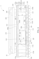
- FIG. 2 is a schematic, cross-sectional diagram showing an exemplary package-on-package (PoP) having thick logic die in accordance with an embodiment of the present disclosure, wherein like layers, regions or elements are designated by like numeral numbers or labels.
- the PoP 1 such as a high-bandwidth PoP (HBPoP) may comprise the semiconductor package 10 as set forth in FIG. 1 and a memory package 20 such as a LPDDR DRAM package stacked on the semiconductor package 10.
- the memory package 20 may comprise a substrate 200, a memory die 210 mounted on the substrate 200, and a molding compound 220 encapsulating the memory die 210.
- the memory package 20 may be electrically connected to the semiconductor package 10 through a plurality of conductive elements 230 such as solder balls or bumps.
- FIG. 3 is a schematic, cross-sectional diagram showing an exemplary package-on-package (PoP) having thick logic die in accordance with another embodiment of the present disclosure, wherein like layers, regions or elements are designated by like numeral numbers or labels.
- the PoP 3 such as a high-bandwidth PoP (HBPoP) may comprise a semiconductor package 10a and a memory package 20 such as a LPDDR DRAM package stacked on the semiconductor package 10a.
- the memory package 20 may comprise a substrate 200, a memory die 210 mounted on the substrate 200, and a molding compound 220 encapsulating the memory die 210.
- the memory package 20 may be electrically connected to the semiconductor package 10a through the plurality of conductive elements 230 such as solder balls or bumps.
- the semiconductor package 10a comprises a bottom substrate 100 having a top surface 100a and an opposing bottom surface 100b.
- the bottom substrate 100 may be a printed wiring board, an interposer substrate, a re-distribution layer (RDL) substrate, or a package substrate having a plurality of conductive interconnect structures 110 and at least an insulating layer 112.
- the conductive interconnect structures 110 may comprise a plurality of pad patterns 110a, 110c, and 110d , and a plurality of pad patterns 110b, wherein the plurality of pad patterns 110a, 110c, and 110d are distributed on the top surface 100a, and the plurality of pad patterns 110b are distributed on the bottom surface 100b.
- a logic die 50 is mounted on the pad patterns 110c on the top surface 100a of the bottom substrate 100 in a flip-chip fashion.
- the logic die 50 may be an application processor die, but is not limited thereto.
- the logic die 50 has a thickness t, wherein t is not less than 125 micrometers, for example, t may be between 125-750 micrometers.
- t is 170 micrometers, which is thicker than a normal logic die (has a thickness of about 80 micrometer) used in high-end mobile devices such as high-end mobile phones.
- the logic die 50 has an active front side 50a and a passive rear side 50b.
- a plurality of input/output (I/O) pads 501 is provided on the active front side 50a.
- the logic die 50 is electrically connected to the pad patterns 110c of the bottom substrate 100 through a plurality of conductive elements 502 such as solder bumps, metal bumps, micro-bumps, or pillars, which are formed on the plurality of I/O pads 501, respectively.
- underfill resin 510 may be injected into a space between the logic die 50 and the top surface 100a of the bottom substrate 100.
- the conductive elements 502 are surrounded by the underfill resin 510.
- an integrated circuit device 80 is mounted in proximity to the logic die 50.
- the integrated circuit device 80 and the logic die 50 are arranged in a side-by-side configuration.
- the integrated circuit device 80 may comprise a modem die 801 and a memory known-good die 802 stacked on the modem die 801.
- the modem die 801 is mounted on the pad patterns 110d of the bottom substrate 100 in a flip-chip fashion.
- the memory known-good die 802 may be mounted on the modem die 801 with an adhesive layer 820 and may be electrically connected to the bottom substrate 100 through a plurality of bond wires BW.
- the integrated circuit device 80 may communicate with the logic die 50 through the bottom substrate 100.
- the modem die 801 and the application processor 50 are mounted on the same bottom substrate 100, better communication between them can be achieved.
- the logic die 50 is an application processor instead of SOC die, the cost can be benefits by increase of gross die per wafer and improved yield with smaller die.
- the logic die 50 and the integrated circuit device 80 are disposed between the bottom substrate 100 and a top substrate 300.
- the top substrate 300 may be a printed wiring board, an interposer substrate, a re-distribution layer (RDL) substrate, or a package substrate having a plurality of conductive interconnect structures 310 and at least an insulating layer 312.
- the conductive interconnect structures 310 may comprise a plurality of pad patterns 310a distributed on the top surface 300a and a plurality of pad patterns 310b distributed on the bottom surface 300b.
- a plurality of copper cored solder balls 60 or other more ductility metal connection is disposed on the pad patterns 310b distributed on the bottom surface 300b of the top substrate 300, respectively.
- the bottom substrate 100 is connected electrically with the top substrate 300 via the copper cored solder balls 60 around the logic die 50 and the integrated circuit device 80.
- the sealing resin SM is filled into a gap having a gap height h between the bottom substrate 100 and the top substrate 300.
- the gap height h is not less than 160 micrometers, for example, h may range between 160-1000 micrometers, but is not limited thereto.
- the pad patterns 110a, on which the copper cored solder balls 60 are attached have a width w ranging between 100-300 micrometers, but is not limited thereto.
- an aspect ratio of the copper cored solder ball 60 may range between 1.1-2.0, for example, 1.44.
- a ball pitch P of the copper cored solder balls 60 may be 0.2-0.3 mm.
- the sealing resin SM surrounds the copper cored solder balls 60 and covers the passive rear side 50b and sidewalls of the logic die 50 and the integrated circuit device 80.
- the sealing resin SM is in direct contact with the bottom surface 300b of the top substrate 300, the side surface of the underfill resin 510 and the top surface 100a of the bottom substrate 100.
- the gap between the bottom substrate 100 and the top substrate 300 is sealed with the sealing resin SM.
- the distance d between the passive rear side 50b of the logic die 50 and the bottom surface 300b of the top substrate 300 may be equal to or greater than 30 micrometers.
- each of the copper cored solder balls 60 may comprise a copper core 602 having a diameter of about 10 micrometers, which is coated with a solder layer 604.
- the copper cored solder balls 60 are joined to the bottom substrate 100 and the top substrate 300.
- the copper core 602 is formed of copper or copper alloys and shaped into a solid sphere.
- the top substrate 300 having the copper cored solder balls 60 may be mounted onto the top surface 100a of the bottom substrate 100 by using a thermal compression bonding (TCB) method.
- TAB thermal compression bonding
- external connection terminals 120 such as solder balls or BGAballs are joined to the pad patterns 110b on the bottom surface 100b of the bottom substrate 100 for further connection with a mother board or a system board.
- a surface mount device 130 such as a capacitor or a resistor may be mounted on the bottom surface 100b of the bottom substrate 100.
- FIG. 4 is a schematic, cross-sectional diagram showing an exemplary package-on-package (PoP) having thick logic die in accordance with still another embodiment of the present disclosure, wherein like layers, regions or elements are designated by like numeral numbers or labels.
- the PoP 4 such as a high-bandwidth PoP (HBPoP) may comprise the semiconductor package 10b and a memory package 20 such as a LPDDR DRAM package stacked on the semiconductor package 10b.
- the memory package 20 may comprise a substrate 200, a memory die 210 mounted on the substrate 200, and a molding compound 220 encapsulating the memory die 210.
- the memory package 20 may be electrically connected to the semiconductor package 10b through a plurality of conductive elements 230 such as solder balls or bumps.
- the semiconductor package 10b comprises a bottom substrate 100 having a top surface 100a and an opposing bottom surface 100b.
- the bottom substrate 100 may be a printed wiring board, an interposer substrate, a re-distribution layer (RDL) substrate, or a package substrate having a plurality of conductive interconnect structures 110 and at least an insulating layer 112.
- the conductive interconnect structures 110 may comprise a plurality of pad patterns 110a, 110c, and 1 10d distributed on the top surface 100a and a plurality of pad patterns 110b distributed on the bottom surface 100b.
- a logic die 50 is mounted on the pad patterns 110c on the top surface 100a of the bottom substrate 100 in a flip-chip fashion.
- the logic die 50 may be an application processor die or a SOC die (usually integrates an application processor and a modem), but is not limited thereto.
- the logic die 50 has a thickness t, wherein t is not less than 125 micrometers, for example, t is between 125-750 micrometers.
- t is 170 micrometers, which is thicker than a normal logic die (has a thickness of about 80 micrometer) used in high-end mobile devices such as high-end mobile phones.
- the logic die 50 has an active front side 50a and a passive rear side 50b.
- a plurality of input/output (I/O) pads 501 is provided on the active front side 50a.
- the logic die 50 is electrically connected to the pad patterns 110c of the bottom substrate 100 through a plurality of conductive elements 502 such as solder bumps, metal bumps, micro-bumps, or pillars, which are formed on the plurality of I/O pads 501, respectively.
- underfill resin 510 may be injected into a space between the logic die 50 and the top surface 100a of the bottom substrate 100.
- the conductive elements 502 are surrounded by the underfill resin 510.
- At least one integrated circuit device may be mounted in proximity to the logic die 50 on the top surface 100a of the bottom substrate 100.
- the at least one integrated circuit device and the logic die 50 are arranged in a side-by-side configuration.
- the at least one integrated circuit device may comprise at least one of a modem, a memory known-good die, a power management IC, and an RF die.
- multiple integrated circuit devices 90a and 90b may be mounted in proximity to the logic die 50 on the top surface 100a of the bottom substrate 100.
- the logic die 50 may be an application processor die
- the integrated circuit devices 90a and 90b may be a modem and a memory known-good die, respectively.
- an integrated circuit devices 90a may be mounted in proximity to the logic die 50 on the top surface 100a of the bottom substrate 100, wherein the logic die 50 may be an application processor die, and the integrated circuit device 90a may be a modem or a memory known-good die. According to another embodiment, an integrated circuit devices 90a may be mounted in proximity to the logic die 50 on the top surface 100a of the bottom substrate 100, wherein the logic die 50 may be a SOC die, and the integrated circuit device 90a may be a power management IC, an RF die.
- the integrated circuit devices 90a and 90b may be mounted in proximity to the logic die 50 on the top surface 100a of the bottom substrate 100, wherein the logic die 50 may be a SOC die, and the integrated circuit devices 90a and 90b may be a power management IC and an RF die, respectively.
- the integrated circuit devices 90a, 90b may be mounted on the pad patterns 110d of the bottom substrate 100 in a flip-chip fashion.
- the integrated circuit devices 90a, 90b may communicate with the logic die 50 through the bottom substrate 100.
- the logic die 50 and the integrated circuit devices 90a, 90b are disposed between the bottom substrate 100 and a top substrate 300.
- the top substrate 300 may be a printed wiring board, an interposer substrate, a re-distribution layer (RDL) substrate, or a package substrate having a plurality of conductive interconnect structures 310 and at least an insulating layer 312.
- the conductive interconnect structures 310 may comprise a plurality of pad patterns 310a distributed on the top surface 300a and a plurality of pad patterns 310b distributed on the bottom surface 300b.
- a plurality of copper cored solder balls 60 or other more ductility metal connection is disposed on the pad patterns 310b distributed on the bottom surface 300b of the top substrate 300, respectively.
- the bottom substrate 100 is connected electrically with the top substrate 300 via the copper cored solder balls 60 around the logic die 50 and the integrated circuit device 80.
- the sealing resin SM is filled into a gap having a gap height h between the bottom substrate 100 and the top substrate 300.
- the gap height h may range between 160-1000 micrometers in 0.2-0.3 mm ball pitch range, but is not limited thereto.
- the pad patterns 110a, on which the copper cored solder balls 60 are attached have a width w ranging between 100-300 micrometers, but is not limited thereto.
- an aspect ratio of the copper cored solder ball 60 may range between 1.1-2.0, for example, 1.44.
- a ball pitch P of the copper cored solder balls 60 may be 0.2-0.3 mm.
- the sealing resin SM surrounds the copper cored solder balls 60 and covers the passive rear side 50b and sidewalls of the logic die 50 and the integrated circuit devices 90a, 90b.
- the sealing resin SM is in direct contact with the bottom surface 300b of the top substrate 300, the side surface of the underfill resin 510 and the top surface 100a of the bottom substrate 100.
- the gap between the bottom substrate 100 and the top substrate 300 is sealed with the sealing resin SM.
- the distance d between the passive rear side 50b of the logic die 50 and the bottom surface 300b of the top substrate 300 may be equal to or greater than 30 micrometers.
- each of the copper cored solder balls 60 may comprise a copper core 602 having a diameter of about 10 micrometers, which is coated with a solder layer 604.
- the copper cored solder balls 60 are joined to the bottom substrate 100 and the top substrate 300.
- the copper core 602 is formed of copper or copper alloys and shaped into a solid sphere.
- the top substrate 300 having the copper cored solder balls 60 may be mounted onto the top surface 100a of the bottom substrate 100 by using a thermal compression bonding (TCB) method.
- TAB thermal compression bonding
- external connection terminals 120 such as solder balls or BGAballs are joined to the pad patterns 110b on the bottom surface 100b of the bottom substrate 100 for further connection with a mother board or a system board.
- a surface mount device 130 such as a capacitor or a resistor may be mounted on the bottom surface 100b of the bottom substrate 100.
Landscapes
- Structures For Mounting Electric Components On Printed Circuit Boards (AREA)
- Structures Or Materials For Encapsulating Or Coating Semiconductor Devices Or Solid State Devices (AREA)
Abstract
Description
- This application is a continuation-in-part of
U.S. Application No. 18/107,520, filed on February 9th, 2023 U.S. Provisional Application No. 63/316,004 U.S. Provisional Application No. 63/354,361 filed on June 22nd, 2022 U.S. Provisional Application No. 63/354,363 filed on June 22nd, 2022 - The present disclosure generally relates to the field of semiconductor packaging. More particularly, the present disclosure relates to a multi-chip module (MCM) package-on-package having a thick logic die.
- Package-on-Package (PoP) is an integrated circuit packaging method to combine vertically discrete logic and memory ball grid array (BGA) packages. Two or more packages are installed atop each other, i.e. stacked, with a standard interface to route signals between them. This allows higher component density in devices, such as mobile phones or digital cameras.
- PoP solutions are commonly used in baseband and applications processors in mobile phones. High-end phones have seen the fastest adoption of PoP packaging to provide high I/O and performance requirements. The main advantage of stacked PoP is that devices can be separately fully tested before assembly.
- With development of the semiconductor industry, many studies are being conducted to improve reliability and durability of the semiconductor packages. An improvement of the PoP structure becomes very important and imperative.
- It is one object of the present disclosure to provide an improved package-on-package in order to solve the above-mentioned prior art deficiencies or shortcomings.
- One aspect of the present disclosure provides a package-on-package, comprising a first package and a second package stacked on the first package. The first package comprises a bottom substrate and a top substrate space apart from the bottom substrate such that the bottom substrate and the top substrate define a gap therebetween; a logic die and at least one integrated circuit device mounted on a top surface of the bottom substrate in a side-by-side configuration, wherein the logic die has a thickness not less than 125 micrometer; a plurality of copper cored solder balls disposed between the bottom substrate and the top substrate around the logic die and the at least one integrated circuit device to electrically connect the bottom substrate with the top substrate; and a sealing resin filling in the gap between the bottom substrate and the top substrate and sealing the logic die, the at least one integrated circuit device, and the plurality of copper cored solder balls in the gap.
- Preferably, the logic die comprises an application processor die or a SOC die.
- Preferably, the logic die has a thickness of 125 -750 micrometers.
- Preferably, the logic die is mounted on the top surface of the bottom substrate in a flip-chip fashion.
- Preferably, the logic die comprises an active front side and a passive rear side, and wherein, a plurality of input/output (I/O) pads is provided on the active front side, and the logic die is electrically connected to the bottom substrate through a plurality of conductive elements formed on the plurality of I/O pads, respectively.
- Preferably, each of the bottom substrate and the top substrate comprises a printed wiring board, an interposer substrate, a re-distribution layer (RDL) substrate, or a package substrate.
- Preferably, the gap has a gap height not less than 160 micrometers.
- Preferably, the gap has a gap height ranging between 160-1000 micrometers.
- Preferably, an aspect ratio of the plurality of copper cored solder balls ranges between 1.1-2.0.
- Preferably, a ball pitch of the plurality of copper cored solder balls is 0.2-0.3 mm.
- Preferably, external connection terminals are disposed on a bottom surface of the bottom substrate.
- Preferably, the second package is a memory package.
- Preferably, the memory package comprises a LPDDR DRAM package.
- Preferably, the at least one integrated circuit device comprise at least one of a modem, a memory known-good die, a power management IC, and an RF die.
- Preferably, the logic die comprises an application processor die, and the at least one integrated circuit device comprises a modem die and a memory known-good die; and wherein the memory known-good die is stacked on the modem die, or the modem die and the memory known-good die are arranged in a side-by-side configuration.
- Preferably, the logic die comprises an application processor die, and the at least one integrated circuit device comprises a modem die.
- Preferably, the logic die comprises a SOC die, and the at least one integrated circuit device comprises a power management IC.
- Preferably, the logic die comprises a SOC die, and the at least one integrated circuit device comprises an RF die.
- These and other objectives of the present invention will no doubt become obvious to those of ordinary skill in the art after reading the following detailed description of the preferred embodiment that is illustrated in the various figures and drawings.
- The accompanying drawings are included to provide a further understanding of the present disclosure and are incorporated in and constitute a part of this specification. The drawings illustrate embodiments of the present disclosure and, together with the description, serve to explain the principles of the present disclosure. In the drawings:
-
FIG. 1 is a schematic, cross-sectional diagram showing an exemplary semiconductor package having thick logic die in accordance with an embodiment of the present disclosure; -
FIG. 2 is a schematic, cross-sectional diagram showing an exemplary package-on-package (PoP) having thick logic die in accordance with an embodiment of the present disclosure; -
FIG. 3 is a schematic, cross-sectional diagram showing an exemplary package-on-package (PoP) having thick logic die in accordance with another embodiment of the present disclosure; and -
FIG. 4 is a schematic, cross-sectional diagram showing an exemplary package-on-package (PoP) having thick logic die in accordance with still another embodiment of the present disclosure. - In the following detailed description of embodiments of the present disclosure, reference is made to the accompanying drawings, which form a part hereof, and in which is shown by way of illustration specific preferred embodiments in which the disclosure may be practiced.
- These embodiments are described in sufficient detail to enable those skilled in the art to practice them, and it is to be understood that other embodiments may be utilized and that mechanical, chemical, electrical, and procedural changes may be made without departing from the scope of the present disclosure. The following detailed description is, therefore, not to be taken in a limiting sense, and the scope of embodiments of the present disclosure is defined only by the appended claims.
- It will be understood that when an element or layer is referred to as being "on", "connected to" or "coupled to" another element or layer, it can be directly on, connected or coupled to the other element or layer or intervening elements or layers may be present. In contrast, when an element is referred to as being "directly on," "directly connected to" or "directly coupled to" another element or layer, there are no intervening elements or layers present. Like numbers refer to like elements throughout. As used herein, the term "and/or" includes any and all combinations of one or more of the associated listed items.
-
FIG. 1 is a schematic, cross-sectional diagram showing an exemplary semiconductor package having thick logic die in accordance with an embodiment of the present disclosure. As shown inFIG. 1 , thesemiconductor package 10 comprises abottom substrate 100 having atop surface 100a and anopposing bottom surface 100b. Preferably, thebottom substrate 100 may be a printed wiring board or a package substrate having a plurality ofconductive interconnect structures 110 and at least aninsulating layer 112. Preferably, theconductive interconnect structures 110 may comprise a plurality ofpad patterns top surface 100a and a plurality ofpad patterns 110b distributed on thebottom surface 100b. - Preferably, a
logic die 50 is mounted on thepad patterns 110c on thetop surface 100a of thebottom substrate 100 in a flip-chip fashion. Preferably, the logic die 50 may be an application processor die or a baseband processor die, but is not limited thereto. Preferably, the logic die 50 has a thickness t ranging between 125-350 micrometers, for example, 170 micrometers, which is thicker than a normal logic die (has a thickness of about 80 micrometer) used in high-end mobile devices such as high-end mobile phones. - Preferably, the logic die 50 has an
active front side 50a and a passiverear side 50b. Preferably, a plurality of input/output (I/O)pads 501 is provided on theactive front side 50a. Preferably, thelogic die 50 is electrically connected to thepad patterns 110c of thebottom substrate 100 through a plurality ofconductive elements 502 such as solder bumps, metal bumps, micro-bumps, or pillars, which are formed on the plurality of I/O pads 501, respectively. Preferably,underfill resin 510 may be injected into a space between the logic die 50 and thetop surface 100a of thebottom substrate 100. Preferably, theconductive elements 502 are surrounded by theunderfill resin 510. Preferably, for example, the I/O pads 501 may be fanned out at the activefront side 50a by using techniques known in the art, for example, a re-distribution layer (RDL) structure. - Preferably, the logic die 50 is disposed between the
bottom substrate 100 and atop substrate 300. Preferably, thetop substrate 300 may be a printed wiring board, an interposer substrate, or a package substrate having a plurality ofconductive interconnect structures 310 and at least aninsulating layer 312. Preferably, theconductive interconnect structures 310 may comprise a plurality ofpad patterns 310a distributed on thetop surface 300a and a plurality ofpad patterns 310b distributed on thebottom surface 300b. Preferably, a plurality of copper coredsolder balls 60 or other more ductility metal connection is disposed on thepad patterns 310b distributed on thebottom surface 300b of thetop substrate 300, respectively. - Preferably, the
bottom substrate 100 is connected electrically with thetop substrate 300 via the copper coredsolder balls 60 around the logic die 50. The sealing resin SM is filled into a gap having a gap height h between thebottom substrate 100 and thetop substrate 300. Preferably, the gap height h may range between 160-450 micrometers in 0.2-0.3 mm ball pitch range, but is not limited thereto. Preferably, thepad patterns 110a, on which the copper coredsolder balls 60 are attached, have a width w ranging between 100-300 micrometers, but is not limited thereto. Preferably, an aspect ratio of the copper coredsolder ball 60 may range between 1.1-2.0, for example, 1.44. Preferably, a ball pitch P of the copper coredsolder balls 60 may be 0.2-0.3 mm. - Preferably, the sealing resin SM surrounds the copper cored
solder balls 60 and covers the passiverear side 50b and sidewalls of the logic die 50. Preferably, the sealing resin SM is in direct contact with thebottom surface 300b of thetop substrate 300, the side surface of theunderfill resin 510 and thetop surface 100a of thebottom substrate 100. The gap between thebottom substrate 100 and thetop substrate 300 is sealed with the sealing resin SM. The distance d between the passiverear side 50b of the logic die 50 and thebottom surface 300b of thetop substrate 300 may be equal to or greater than 30 micrometers. - Preferably, each of the copper cored
solder balls 60 may comprise acopper core 602 having a diameter of about 10 micrometers, which is coated with asolder layer 604. The copper coredsolder balls 60 are joined to thebottom substrate 100 and thetop substrate 300. Preferably, thecopper core 602 is formed of copper or copper alloys and shaped into a solid sphere. Preferably, thetop substrate 300 having the copper coredsolder balls 60 may be mounted onto thetop surface 100a of thebottom substrate 100 by using a thermal compression bonding (TCB) method. - Preferably,
external connection terminals 120 such as solder balls or BGA balls are joined to thepad patterns 110b on thebottom surface 100b of thebottom substrate 100 for further connection with a mother board or a system board. Preferably, asurface mount device 130 such as a capacitor or a resistor may be mounted on thebottom surface 100b of thebottom substrate 100. -
FIG. 2 is a schematic, cross-sectional diagram showing an exemplary package-on-package (PoP) having thick logic die in accordance with an embodiment of the present disclosure, wherein like layers, regions or elements are designated by like numeral numbers or labels. As shown inFIG. 2 , thePoP 1 such as a high-bandwidth PoP (HBPoP) may comprise thesemiconductor package 10 as set forth inFIG. 1 and amemory package 20 such as a LPDDR DRAM package stacked on thesemiconductor package 10. Preferably, thememory package 20 may comprise asubstrate 200, a memory die 210 mounted on thesubstrate 200, and amolding compound 220 encapsulating the memory die 210. Preferably, thememory package 20 may be electrically connected to thesemiconductor package 10 through a plurality ofconductive elements 230 such as solder balls or bumps. -
FIG. 3 is a schematic, cross-sectional diagram showing an exemplary package-on-package (PoP) having thick logic die in accordance with another embodiment of the present disclosure, wherein like layers, regions or elements are designated by like numeral numbers or labels. As shown inFIG. 3 , the PoP 3 such as a high-bandwidth PoP (HBPoP) may comprise asemiconductor package 10a and amemory package 20 such as a LPDDR DRAM package stacked on thesemiconductor package 10a. Preferably, thememory package 20 may comprise asubstrate 200, a memory die 210 mounted on thesubstrate 200, and amolding compound 220 encapsulating the memory die 210. Preferably, thememory package 20 may be electrically connected to thesemiconductor package 10a through the plurality ofconductive elements 230 such as solder balls or bumps. - Preferably, likewise, the
semiconductor package 10a comprises abottom substrate 100 having atop surface 100a and an opposingbottom surface 100b. Preferably, thebottom substrate 100 may be a printed wiring board, an interposer substrate, a re-distribution layer (RDL) substrate, or a package substrate having a plurality ofconductive interconnect structures 110 and at least aninsulating layer 112. Preferably, theconductive interconnect structures 110 may comprise a plurality ofpad patterns pad patterns 110b, wherein the plurality ofpad patterns top surface 100a, and the plurality ofpad patterns 110b are distributed on thebottom surface 100b. - Preferably, a
logic die 50 is mounted on thepad patterns 110c on thetop surface 100a of thebottom substrate 100 in a flip-chip fashion. Preferably, the logic die 50 may be an application processor die, but is not limited thereto. Preferably, the logic die 50 has a thickness t, wherein t is not less than 125 micrometers, for example, t may be between 125-750 micrometers. Preferably, t is 170 micrometers, which is thicker than a normal logic die (has a thickness of about 80 micrometer) used in high-end mobile devices such as high-end mobile phones. Preferably, the logic die 50 has an activefront side 50a and a passiverear side 50b. Preferably, a plurality of input/output (I/O)pads 501 is provided on the activefront side 50a. Preferably, the logic die 50 is electrically connected to thepad patterns 110c of thebottom substrate 100 through a plurality ofconductive elements 502 such as solder bumps, metal bumps, micro-bumps, or pillars, which are formed on the plurality of I/O pads 501, respectively. Preferably,underfill resin 510 may be injected into a space between the logic die 50 and thetop surface 100a of thebottom substrate 100. Preferably, theconductive elements 502 are surrounded by theunderfill resin 510. - Preferably, an
integrated circuit device 80 is mounted in proximity to the logic die 50. Preferably, theintegrated circuit device 80 and the logic die 50 are arranged in a side-by-side configuration. Preferably, theintegrated circuit device 80 may comprise a modem die 801 and a memory known-good die 802 stacked on the modem die 801. Preferably, the modem die 801 is mounted on thepad patterns 110d of thebottom substrate 100 in a flip-chip fashion. The memory known-good die 802 may be mounted on the modem die 801 with anadhesive layer 820 and may be electrically connected to thebottom substrate 100 through a plurality of bond wires BW. Preferably, theintegrated circuit device 80 may communicate with the logic die 50 through thebottom substrate 100. - It is advantageous to use this embodiment because the modem die 801 and the
application processor 50 are mounted on thesame bottom substrate 100, better communication between them can be achieved. Furthermore, in this embodiment, the logic die 50 is an application processor instead of SOC die, the cost can be benefits by increase of gross die per wafer and improved yield with smaller die. - Preferably, the logic die 50 and the
integrated circuit device 80 are disposed between thebottom substrate 100 and atop substrate 300. Preferably, thetop substrate 300 may be a printed wiring board, an interposer substrate, a re-distribution layer (RDL) substrate, or a package substrate having a plurality ofconductive interconnect structures 310 and at least aninsulating layer 312. Preferably, theconductive interconnect structures 310 may comprise a plurality ofpad patterns 310a distributed on thetop surface 300a and a plurality ofpad patterns 310b distributed on thebottom surface 300b. Preferably, a plurality of copper coredsolder balls 60 or other more ductility metal connection is disposed on thepad patterns 310b distributed on thebottom surface 300b of thetop substrate 300, respectively. - Preferably, the
bottom substrate 100 is connected electrically with thetop substrate 300 via the copper coredsolder balls 60 around the logic die 50 and theintegrated circuit device 80. The sealing resin SM is filled into a gap having a gap height h between thebottom substrate 100 and thetop substrate 300. Preferably, the gap height h is not less than 160 micrometers, for example, h may range between 160-1000 micrometers, but is not limited thereto. Preferably, thepad patterns 110a, on which the copper coredsolder balls 60 are attached, have a width w ranging between 100-300 micrometers, but is not limited thereto. Preferably, an aspect ratio of the copper coredsolder ball 60 may range between 1.1-2.0, for example, 1.44. Preferably, a ball pitch P of the copper coredsolder balls 60 may be 0.2-0.3 mm. - Preferably, the sealing resin SM surrounds the copper cored
solder balls 60 and covers the passiverear side 50b and sidewalls of the logic die 50 and theintegrated circuit device 80. Preferably, the sealing resin SM is in direct contact with thebottom surface 300b of thetop substrate 300, the side surface of theunderfill resin 510 and thetop surface 100a of thebottom substrate 100. The gap between thebottom substrate 100 and thetop substrate 300 is sealed with the sealing resin SM. The distance d between the passiverear side 50b of the logic die 50 and thebottom surface 300b of thetop substrate 300 may be equal to or greater than 30 micrometers. - Preferably, each of the copper cored
solder balls 60 may comprise acopper core 602 having a diameter of about 10 micrometers, which is coated with asolder layer 604. The copper coredsolder balls 60 are joined to thebottom substrate 100 and thetop substrate 300. Preferably, thecopper core 602 is formed of copper or copper alloys and shaped into a solid sphere. Preferably, thetop substrate 300 having the copper coredsolder balls 60 may be mounted onto thetop surface 100a of thebottom substrate 100 by using a thermal compression bonding (TCB) method. - Preferably, likewise,
external connection terminals 120 such as solder balls or BGAballs are joined to thepad patterns 110b on thebottom surface 100b of thebottom substrate 100 for further connection with a mother board or a system board. Preferably, asurface mount device 130 such as a capacitor or a resistor may be mounted on thebottom surface 100b of thebottom substrate 100. -
FIG. 4 is a schematic, cross-sectional diagram showing an exemplary package-on-package (PoP) having thick logic die in accordance with still another embodiment of the present disclosure, wherein like layers, regions or elements are designated by like numeral numbers or labels. As shown inFIG. 4 , thePoP 4 such as a high-bandwidth PoP (HBPoP) may comprise thesemiconductor package 10b and amemory package 20 such as a LPDDR DRAM package stacked on thesemiconductor package 10b. Preferably, thememory package 20 may comprise asubstrate 200, a memory die 210 mounted on thesubstrate 200, and amolding compound 220 encapsulating the memory die 210. Preferably, thememory package 20 may be electrically connected to thesemiconductor package 10b through a plurality ofconductive elements 230 such as solder balls or bumps. - Preferably, likewise, the
semiconductor package 10b comprises abottom substrate 100 having atop surface 100a and an opposingbottom surface 100b. Preferably, thebottom substrate 100 may be a printed wiring board, an interposer substrate, a re-distribution layer (RDL) substrate, or a package substrate having a plurality ofconductive interconnect structures 110 and at least aninsulating layer 112. Preferably, theconductive interconnect structures 110 may comprise a plurality ofpad patterns top surface 100a and a plurality ofpad patterns 110b distributed on thebottom surface 100b. - Preferably, a
logic die 50 is mounted on thepad patterns 110c on thetop surface 100a of thebottom substrate 100 in a flip-chip fashion. Preferably, the logic die 50 may be an application processor die or a SOC die (usually integrates an application processor and a modem), but is not limited thereto. Preferably, the logic die 50 has a thickness t, wherein t is not less than 125 micrometers, for example, t is between 125-750 micrometers. Preferably, t is 170 micrometers, which is thicker than a normal logic die (has a thickness of about 80 micrometer) used in high-end mobile devices such as high-end mobile phones. Preferably, the logic die 50 has an activefront side 50a and a passiverear side 50b. Preferably, a plurality of input/output (I/O)pads 501 is provided on the activefront side 50a. Preferably, the logic die 50 is electrically connected to thepad patterns 110c of thebottom substrate 100 through a plurality ofconductive elements 502 such as solder bumps, metal bumps, micro-bumps, or pillars, which are formed on the plurality of I/O pads 501, respectively. Preferably,underfill resin 510 may be injected into a space between the logic die 50 and thetop surface 100a of thebottom substrate 100. Preferably, theconductive elements 502 are surrounded by theunderfill resin 510. - Preferably, at least one integrated circuit device may be mounted in proximity to the logic die 50 on the
top surface 100a of thebottom substrate 100. The at least one integrated circuit device and the logic die 50 are arranged in a side-by-side configuration. For example, but not limited to, the at least one integrated circuit device may comprise at least one of a modem, a memory known-good die, a power management IC, and an RF die. Preferably, multipleintegrated circuit devices top surface 100a of thebottom substrate 100. Preferably, wherein the logic die 50 may be an application processor die, and theintegrated circuit devices integrated circuit devices 90a may be mounted in proximity to the logic die 50 on thetop surface 100a of thebottom substrate 100, wherein the logic die 50 may be an application processor die, and theintegrated circuit device 90a may be a modem or a memory known-good die. According to another embodiment, anintegrated circuit devices 90a may be mounted in proximity to the logic die 50 on thetop surface 100a of thebottom substrate 100, wherein the logic die 50 may be a SOC die, and theintegrated circuit device 90a may be a power management IC, an RF die. According to another embodiment, theintegrated circuit devices top surface 100a of thebottom substrate 100, wherein the logic die 50 may be a SOC die, and theintegrated circuit devices - Preferably, the
integrated circuit devices pad patterns 110d of thebottom substrate 100 in a flip-chip fashion. Preferably, theintegrated circuit devices bottom substrate 100. - Preferably, the logic die 50 and the
integrated circuit devices bottom substrate 100 and atop substrate 300. Preferably, thetop substrate 300 may be a printed wiring board, an interposer substrate, a re-distribution layer (RDL) substrate, or a package substrate having a plurality ofconductive interconnect structures 310 and at least aninsulating layer 312. Preferably, theconductive interconnect structures 310 may comprise a plurality ofpad patterns 310a distributed on thetop surface 300a and a plurality ofpad patterns 310b distributed on thebottom surface 300b. Preferably, a plurality of copper coredsolder balls 60 or other more ductility metal connection is disposed on thepad patterns 310b distributed on thebottom surface 300b of thetop substrate 300, respectively. - Preferably, the
bottom substrate 100 is connected electrically with thetop substrate 300 via the copper coredsolder balls 60 around the logic die 50 and theintegrated circuit device 80. The sealing resin SM is filled into a gap having a gap height h between thebottom substrate 100 and thetop substrate 300. Preferably, the gap height h may range between 160-1000 micrometers in 0.2-0.3 mm ball pitch range, but is not limited thereto. Preferably, thepad patterns 110a, on which the copper coredsolder balls 60 are attached, have a width w ranging between 100-300 micrometers, but is not limited thereto. Preferably, an aspect ratio of the copper coredsolder ball 60 may range between 1.1-2.0, for example, 1.44. Preferably, a ball pitch P of the copper coredsolder balls 60 may be 0.2-0.3 mm. - Preferably, the sealing resin SM surrounds the copper cored
solder balls 60 and covers the passiverear side 50b and sidewalls of the logic die 50 and theintegrated circuit devices bottom surface 300b of thetop substrate 300, the side surface of theunderfill resin 510 and thetop surface 100a of thebottom substrate 100. The gap between thebottom substrate 100 and thetop substrate 300 is sealed with the sealing resin SM. The distance d between the passiverear side 50b of the logic die 50 and thebottom surface 300b of thetop substrate 300 may be equal to or greater than 30 micrometers. - Preferably, each of the copper cored
solder balls 60 may comprise acopper core 602 having a diameter of about 10 micrometers, which is coated with asolder layer 604. The copper coredsolder balls 60 are joined to thebottom substrate 100 and thetop substrate 300. Preferably, thecopper core 602 is formed of copper or copper alloys and shaped into a solid sphere. Preferably, thetop substrate 300 having the copper coredsolder balls 60 may be mounted onto thetop surface 100a of thebottom substrate 100 by using a thermal compression bonding (TCB) method. - Preferably, likewise,
external connection terminals 120 such as solder balls or BGAballs are joined to thepad patterns 110b on thebottom surface 100b of thebottom substrate 100 for further connection with a mother board or a system board. Preferably, asurface mount device 130 such as a capacitor or a resistor may be mounted on thebottom surface 100b of thebottom substrate 100. - Those skilled in the art will readily observe that numerous modifications and alterations of the device and method may be made while retaining the teachings of the present disclosure. Accordingly, the above disclosure should be construed as limited only by the metes and bounds of the appended claims.
Claims (15)
- A package-on-package (3), comprising a first package (10) and a second package (20) stacked on the first package, wherein the first package (10) comprises:a bottom substrate (100) and a top substrate (300) space apart from the bottom substrate (100) such that the bottom substrate (100) and the top substrate (300) define a gap therebetween;a logic die (50) and at least one integrated circuit device (80) mounted on a top surface (100a) of the bottom substrate (100) in a side-by-side configuration, wherein the logic die (50) has a thickness not less than 125 micrometer;a plurality of copper cored solder balls (60) disposed between the bottom substrate (100) and the top substrate (300) around the logic die (50) and the at least one integrated circuit device (80) to electrically connect the bottom substrate (100) with the top substrate (300); anda sealing resin (SM) filling in the gap between the bottom substrate (100) and the top substrate (300) and sealing the logic die (50), the at least one integrated circuit device (80), and the plurality of copper cored solder balls (60) in the gap.
- The package-on-package (3) according to claim 1, wherein the logic die (50) comprises an application processor die or a SOC die.
- The package-on-package (3) according to claim 1 or 2, wherein the logic die (50) has a thickness of 125 -750 micrometers.
- The package-on-package (3) according to any one of claims 1 to 3, wherein the logic die (50) is mounted on the top surface (100a) of the bottom substrate (100) in a flip-chip fashion.
- The package-on-package (3) according to claim 4, wherein the logic die (50) comprises an active front side (50a) and a passive rear side (50b), and wherein, a plurality of input/output, in the following also referred to as I/O, pads (501) is provided on the active front side (50a), and the logic die (50) is electrically connected to the bottom substrate (100) through a plurality of conductive elements (502) formed on the plurality of I/O pads (501), respectively.
- The package-on-package (3) according to any one of claims 1 to 5, wherein each of the bottom substrate (100) and the top substrate (300) comprises a printed wiring board, an interposer substrate, a re-distribution layer, in the following also referred to as RDL, substrate, or a package
- The package-on-package (3) according to any one of claims 1 to 6, wherein the gap has a gap height (h) not less than 160 micrometers; and/or
wherein the gap has a gap height (h) ranging between 160-1000 micrometers. - The package-on-package (3) according to any one of claims 1 to 7, wherein an aspect ratio of the plurality of copper cored solder balls (60) ranges between 1.1-2.0.
- The package-on-package (3) according to any one of claims 1 to 8, wherein a ball pitch of the plurality of copper cored solder balls (60) is 0.2-0.3 mm.
- The package-on-package (3) according to any one of claims 1 to 9, wherein external connection terminals (120) are disposed on a bottom surface (100b) of the bottom substrate (100).
- The package-on-package (3) according to any one of claims 1 to 10, wherein the second package (20) is a memory package.
- The package-on-package (3) according to claim 11, wherein the memory package comprises an LPDDR DRAM package.
- The package-on-package (3) according to any one of claims 1 to 12, wherein the at least one integrated circuit device (80) comprises at least one of a modem, a memory known-good die, a power management IC, and an RF die.
- The package-on-package (3) according to any one of claims 1 to 13, wherein the logic die (50) comprises an application processor die, and the at least one integrated circuit device (80) comprises a modem die and a memory known-good die; and
wherein the memory known-good die is stacked on the modem die, or the modem die and the memory known-good die are arranged in a side-by-side configuration. - The package-on-package (3) according to any one of claims 1 to 14, wherein the logic die (50) comprises an application processor die, and the at least one integrated circuit device (80) comprises a modem die; and/orwherein the logic die (50) comprises a SOC die, and the at least one integrated circuit device (80) comprises a power management IC; and/orwherein the logic die (50) comprises a SOC die, and the at least one integrated circuit device (80) comprises an RF die.
Applications Claiming Priority (4)
| Application Number | Priority Date | Filing Date | Title |
|---|---|---|---|
| US202263354363P | 2022-06-22 | 2022-06-22 | |
| US202263354361P | 2022-06-22 | 2022-06-22 | |
| US18/107,520 US20230282625A1 (en) | 2022-03-03 | 2023-02-09 | Semiconductor package having a thick logic die |
| US18/203,631 US20230307421A1 (en) | 2022-03-03 | 2023-05-30 | Package-on-package having a thick logic die |
Publications (1)
| Publication Number | Publication Date |
|---|---|
| EP4300567A1 true EP4300567A1 (en) | 2024-01-03 |
Family
ID=86760659
Family Applications (1)
| Application Number | Title | Priority Date | Filing Date |
|---|---|---|---|
| EP23179942.0A Pending EP4300567A1 (en) | 2022-06-22 | 2023-06-19 | Package-on-package having a thick logic die |
Country Status (2)
| Country | Link |
|---|---|
| EP (1) | EP4300567A1 (en) |
| TW (1) | TW202401693A (en) |
Citations (2)
| Publication number | Priority date | Publication date | Assignee | Title |
|---|---|---|---|---|
| US20210257305A1 (en) * | 2020-02-18 | 2021-08-19 | Samsung Electronics Co., Ltd. | Semiconductor package, and package on package having the same |
| CN113410206A (en) * | 2020-03-17 | 2021-09-17 | 安靠科技新加坡控股私人有限公司 | Semiconductor device and method for manufacturing semiconductor device |
-
2023
- 2023-06-15 TW TW112122406A patent/TW202401693A/en unknown
- 2023-06-19 EP EP23179942.0A patent/EP4300567A1/en active Pending
Patent Citations (2)
| Publication number | Priority date | Publication date | Assignee | Title |
|---|---|---|---|---|
| US20210257305A1 (en) * | 2020-02-18 | 2021-08-19 | Samsung Electronics Co., Ltd. | Semiconductor package, and package on package having the same |
| CN113410206A (en) * | 2020-03-17 | 2021-09-17 | 安靠科技新加坡控股私人有限公司 | Semiconductor device and method for manufacturing semiconductor device |
Also Published As
| Publication number | Publication date |
|---|---|
| TW202401693A (en) | 2024-01-01 |
Similar Documents
| Publication | Publication Date | Title |
|---|---|---|
| US9449941B2 (en) | Connecting function chips to a package to form package-on-package | |
| US7901987B2 (en) | Package-on-package system with internal stacking module interposer | |
| US5977640A (en) | Highly integrated chip-on-chip packaging | |
| US6768190B2 (en) | Stack type flip-chip package | |
| KR101623880B1 (en) | Semiconductor package | |
| EP3258486A1 (en) | Semiconductor package incorporating redistribution layer interposer | |
| US20170243858A1 (en) | Semiconductor package incorporating redistribution layer interposer | |
| US20040070083A1 (en) | Stacked flip-chip package | |
| TWI818458B (en) | Electronic package and manufacturing method thereof | |
| US20250210527A1 (en) | Electronic Package and Manufacturing Method Thereof | |
| EP4167690B1 (en) | Electronic device with stacked printed circuit boards | |
| US20220320043A1 (en) | Semiconductor package and method of fabricating the same | |
| EP4297077A2 (en) | Semiconductor package having a thick logic die | |
| US20230307421A1 (en) | Package-on-package having a thick logic die | |
| US6570246B1 (en) | Multi-die package | |
| US20060220208A1 (en) | Stacked-type semiconductor device and method of manufacturing the same | |
| CN117276266A (en) | A stacked package | |
| EP4266361A1 (en) | Semiconductor package having a thick logic die | |
| US20230282604A1 (en) | Semiconductor package having a thick logic die | |
| TW202401693A (en) | A package-on-package | |
| CN118073319A (en) | Packaging structure and packaging method | |
| TWI890558B (en) | Electronic package and manufacturing method thereof | |
| US20250183239A1 (en) | Electronic package and manufacturing method thereof | |
| US12368104B2 (en) | Electronic package | |
| CN221783207U (en) | Chip packaging structure and electronic equipment |
Legal Events
| Date | Code | Title | Description |
|---|---|---|---|
| PUAI | Public reference made under article 153(3) epc to a published international application that has entered the european phase |
Free format text: ORIGINAL CODE: 0009012 |
|
| STAA | Information on the status of an ep patent application or granted ep patent |
Free format text: STATUS: THE APPLICATION HAS BEEN PUBLISHED |
|
| AK | Designated contracting states |
Kind code of ref document: A1 Designated state(s): AL AT BE BG CH CY CZ DE DK EE ES FI FR GB GR HR HU IE IS IT LI LT LU LV MC ME MK MT NL NO PL PT RO RS SE SI SK SM TR |
|
| STAA | Information on the status of an ep patent application or granted ep patent |
Free format text: STATUS: REQUEST FOR EXAMINATION WAS MADE |
|
| 17P | Request for examination filed |
Effective date: 20240528 |
|
| RBV | Designated contracting states (corrected) |
Designated state(s): AL AT BE BG CH CY CZ DE DK EE ES FI FR GB GR HR HU IE IS IT LI LT LU LV MC ME MK MT NL NO PL PT RO RS SE SI SK SM TR |