EP4300522A1 - Contactless power feeding system - Google Patents
Contactless power feeding system Download PDFInfo
- Publication number
- EP4300522A1 EP4300522A1 EP22759320.9A EP22759320A EP4300522A1 EP 4300522 A1 EP4300522 A1 EP 4300522A1 EP 22759320 A EP22759320 A EP 22759320A EP 4300522 A1 EP4300522 A1 EP 4300522A1
- Authority
- EP
- European Patent Office
- Prior art keywords
- coil
- primary
- capacitance
- tertiary
- capacitor
- Prior art date
- Legal status (The legal status is an assumption and is not a legal conclusion. Google has not performed a legal analysis and makes no representation as to the accuracy of the status listed.)
- Pending
Links
- 239000003990 capacitor Substances 0.000 claims abstract description 187
- 230000005540 biological transmission Effects 0.000 claims abstract description 76
- 230000008878 coupling Effects 0.000 claims description 39
- 238000010168 coupling process Methods 0.000 claims description 39
- 238000005859 coupling reaction Methods 0.000 claims description 39
- 230000007423 decrease Effects 0.000 claims description 24
- 238000001514 detection method Methods 0.000 description 21
- 230000002457 bidirectional effect Effects 0.000 description 20
- 230000003247 decreasing effect Effects 0.000 description 18
- 230000004907 flux Effects 0.000 description 12
- 230000009467 reduction Effects 0.000 description 12
- 238000004088 simulation Methods 0.000 description 11
- 230000001965 increasing effect Effects 0.000 description 8
- 230000008859 change Effects 0.000 description 7
- 238000006243 chemical reaction Methods 0.000 description 6
- 230000000052 comparative effect Effects 0.000 description 5
- 230000009286 beneficial effect Effects 0.000 description 4
- 230000008901 benefit Effects 0.000 description 4
- 230000001939 inductive effect Effects 0.000 description 4
- 230000010349 pulsation Effects 0.000 description 4
- 239000004020 conductor Substances 0.000 description 3
- 230000003111 delayed effect Effects 0.000 description 2
- 230000000694 effects Effects 0.000 description 2
- 230000005611 electricity Effects 0.000 description 2
- 238000004519 manufacturing process Methods 0.000 description 2
- 230000001105 regulatory effect Effects 0.000 description 2
- 238000004804 winding Methods 0.000 description 2
- 238000004364 calculation method Methods 0.000 description 1
- 230000005674 electromagnetic induction Effects 0.000 description 1
- 230000004048 modification Effects 0.000 description 1
- 238000012986 modification Methods 0.000 description 1
- 230000003071 parasitic effect Effects 0.000 description 1
- 230000002093 peripheral effect Effects 0.000 description 1
Images


Classifications
-
- H—ELECTRICITY
- H02—GENERATION; CONVERSION OR DISTRIBUTION OF ELECTRIC POWER
- H02J—CIRCUIT ARRANGEMENTS OR SYSTEMS FOR SUPPLYING OR DISTRIBUTING ELECTRIC POWER; SYSTEMS FOR STORING ELECTRIC ENERGY
- H02J50/00—Circuit arrangements or systems for wireless supply or distribution of electric power
- H02J50/10—Circuit arrangements or systems for wireless supply or distribution of electric power using inductive coupling
- H02J50/12—Circuit arrangements or systems for wireless supply or distribution of electric power using inductive coupling of the resonant type
-
- B—PERFORMING OPERATIONS; TRANSPORTING
- B60—VEHICLES IN GENERAL
- B60L—PROPULSION OF ELECTRICALLY-PROPELLED VEHICLES; SUPPLYING ELECTRIC POWER FOR AUXILIARY EQUIPMENT OF ELECTRICALLY-PROPELLED VEHICLES; ELECTRODYNAMIC BRAKE SYSTEMS FOR VEHICLES IN GENERAL; MAGNETIC SUSPENSION OR LEVITATION FOR VEHICLES; MONITORING OPERATING VARIABLES OF ELECTRICALLY-PROPELLED VEHICLES; ELECTRIC SAFETY DEVICES FOR ELECTRICALLY-PROPELLED VEHICLES
- B60L53/00—Methods of charging batteries, specially adapted for electric vehicles; Charging stations or on-board charging equipment therefor; Exchange of energy storage elements in electric vehicles
- B60L53/10—Methods of charging batteries, specially adapted for electric vehicles; Charging stations or on-board charging equipment therefor; Exchange of energy storage elements in electric vehicles characterised by the energy transfer between the charging station and the vehicle
- B60L53/12—Inductive energy transfer
- B60L53/122—Circuits or methods for driving the primary coil, e.g. supplying electric power to the coil
-
- B—PERFORMING OPERATIONS; TRANSPORTING
- B60—VEHICLES IN GENERAL
- B60L—PROPULSION OF ELECTRICALLY-PROPELLED VEHICLES; SUPPLYING ELECTRIC POWER FOR AUXILIARY EQUIPMENT OF ELECTRICALLY-PROPELLED VEHICLES; ELECTRODYNAMIC BRAKE SYSTEMS FOR VEHICLES IN GENERAL; MAGNETIC SUSPENSION OR LEVITATION FOR VEHICLES; MONITORING OPERATING VARIABLES OF ELECTRICALLY-PROPELLED VEHICLES; ELECTRIC SAFETY DEVICES FOR ELECTRICALLY-PROPELLED VEHICLES
- B60L53/00—Methods of charging batteries, specially adapted for electric vehicles; Charging stations or on-board charging equipment therefor; Exchange of energy storage elements in electric vehicles
- B60L53/30—Constructional details of charging stations
- B60L53/35—Means for automatic or assisted adjustment of the relative position of charging devices and vehicles
- B60L53/38—Means for automatic or assisted adjustment of the relative position of charging devices and vehicles specially adapted for charging by inductive energy transfer
- B60L53/39—Means for automatic or assisted adjustment of the relative position of charging devices and vehicles specially adapted for charging by inductive energy transfer with position-responsive activation of primary coils
-
- B—PERFORMING OPERATIONS; TRANSPORTING
- B60—VEHICLES IN GENERAL
- B60M—POWER SUPPLY LINES, AND DEVICES ALONG RAILS, FOR ELECTRICALLY- PROPELLED VEHICLES
- B60M7/00—Power lines or rails specially adapted for electrically-propelled vehicles of special types, e.g. suspension tramway, ropeway, underground railway
-
- H—ELECTRICITY
- H01—ELECTRIC ELEMENTS
- H01F—MAGNETS; INDUCTANCES; TRANSFORMERS; SELECTION OF MATERIALS FOR THEIR MAGNETIC PROPERTIES
- H01F38/00—Adaptations of transformers or inductances for specific applications or functions
- H01F38/14—Inductive couplings
-
- H—ELECTRICITY
- H02—GENERATION; CONVERSION OR DISTRIBUTION OF ELECTRIC POWER
- H02J—CIRCUIT ARRANGEMENTS OR SYSTEMS FOR SUPPLYING OR DISTRIBUTING ELECTRIC POWER; SYSTEMS FOR STORING ELECTRIC ENERGY
- H02J50/00—Circuit arrangements or systems for wireless supply or distribution of electric power
- H02J50/40—Circuit arrangements or systems for wireless supply or distribution of electric power using two or more transmitting or receiving devices
-
- H—ELECTRICITY
- H02—GENERATION; CONVERSION OR DISTRIBUTION OF ELECTRIC POWER
- H02J—CIRCUIT ARRANGEMENTS OR SYSTEMS FOR SUPPLYING OR DISTRIBUTING ELECTRIC POWER; SYSTEMS FOR STORING ELECTRIC ENERGY
- H02J50/00—Circuit arrangements or systems for wireless supply or distribution of electric power
- H02J50/90—Circuit arrangements or systems for wireless supply or distribution of electric power involving detection or optimisation of position, e.g. alignment
-
- H—ELECTRICITY
- H02—GENERATION; CONVERSION OR DISTRIBUTION OF ELECTRIC POWER
- H02J—CIRCUIT ARRANGEMENTS OR SYSTEMS FOR SUPPLYING OR DISTRIBUTING ELECTRIC POWER; SYSTEMS FOR STORING ELECTRIC ENERGY
- H02J7/00—Circuit arrangements for charging or depolarising batteries or for supplying loads from batteries
Definitions
- This disclosure relates generally to a wireless power transmission system.
- Japanese translation of PCT application publication No. 2002-508916 discloses an inductive power transfer system which works to transfer electric power from a primary inductive conductor (i.e., primary coil) to a secondary resonance pickup circuit through an intermediate resonance loop which resonates at a system frequency.
- a wireless power transmission system which works to supply electric power wirelessly from a power transmitter to a power receiver.
- the wireless power transmission system comprises: (a) a power transmitter which includes a primary resonant circuit and an alternating-current source, the primary resonant circuit including a primary coil and a primary capacitor for use in power transmission, the alternating-current source working to apply ac power at a given operating frequency to the primary resonant circuit; (b) a power receiver which includes a secondary resonant circuit, the secondary resonant circuit including a secondary coil and a secondary capacitor for use in a power reception, the secondary coil being to be magnetically coupled with the primary coil; and (c) a tertiary resonant circuit which includes a tertiary coil and a tertiary capacitor.
- the tertiary coil is arranged to achieve magnetic coupling with the primary coil and the secondary coil.
- the tertiary capacitor constitutes a short-circuit resonant circuit along with the tertiary coil.
- the primary coil has a self-inductance L1.
- a capacitance of the primary capacitor is set to a capacitance C1, as given by Eq. (1) below, to cause resonance in the primary capacitor and the primary coil at an angular frequency ⁇ 0 that is the operating frequency.
- C 1 1 ⁇ o 2 ⁇ L 1
- the tertiary coil has a self-inductance L3.
- a capacitance of the tertiary capacitor is set to a capacitance C3, as given by Eq. (2) below, to cause resonance in the tertiary capacitor and the tertiary coil at the operating frequency.
- C 3 1 ⁇ o 2 ⁇ L 3
- a capacitance of the secondary capacitor is determined to decrease a reactive component of the ac power which arises from the self-inductances and mutual inductances of the primary coil, the secondary coil, and the tertiary coil.
- the wireless power transmission system When electrical energy is transferred from the power transmitter to the power receiver, the wireless power transmission system is capable of decreasing a reactive component of ac power applied from the alternating-current source to the primary resonant circuit, thereby minimizing a drop in power factor of the ac power supplied to the primary resonant circuit. This reduces a loss of energy in the alternating-current source. For instance, in a case where the alternating-current source is equipped with an inverter and a filter, an energy loss is reduced in the inverter and the filter.
- the above structure of the wireless power transmission system is also capable of determining the capacitance of the primary capacitor of the primary resonant circuit and the capacitance of the tertiary capacitor of the tertiary resonant circuit regardless of coupling coefficients of the primary coil, the secondary coil, and the tertiary coil, thereby resulting in an increase in available types of the power receiver to which electrical energy is transferred from the power transmitter
- a wireless power transmission system in the first embodiment includes the power transmitter 100, the power receiver 200, and the tertiary resonant circuit 310.
- the power receiver 200 receives electric power wirelessly delivered from the power transmitter 100.
- the power transmitter 100 includes the primary resonant circuit 110 and the alternating-current source 130.
- the primary resonant circuit 110 is an electrical circuit working to supply electric power to the power receiver 200 using electromagnetic induction due to resonance.
- the primary resonant circuit 110 includes the primary coil 112 and the primary capacitor 114 connected directly to the primary coil 112.
- the primary capacitor 114 functions as a resonant capacitor to resonate electric power applied to the primary coil 112.
- the alternating-current source 130 is a device working to apply an ac power at a preselected operating frequency f0 (i.e., angular frequency ⁇ 0 ) to the primary resonant circuit 110.
- the alternating-current source 130 includes a power supply device which converts an ac power produced by an external power supply into a dc power and an inverter which works to convert the dc power delivered from the power supply device into an ac power at an operating frequency.
- the alternating-current source 130 may also include a filter following the inverter in the signal path.
- the power receiver 200 may be installed in a variety of devices, such as electronic devices or electric automobiles, which are operated using electric power.
- the power receiver 200 includes the secondary resonant circuit 210, the power receiving circuit 220, and the battery 230.
- the secondary resonant circuit 210 like the primary resonant circuit 110, includes the secondary coil 212 and the secondary capacitor 214 which is connected in series with the secondary coil 212 and serves as a resonant capacitor.
- the secondary resonant circuit 210 is a circuit which obtains ac power, as induced in the secondary coil 212, when the secondary coil 212 and the primary coil 112 are in magnetic resonant coupling with each other.
- the power receiving circuit 220 is a device working to convert ac power, as derived in the secondary resonant circuit 210, into dc power to charge the battery 230.
- the electrical energy stored in the battery 230 is used as electric power in a device in which the power receiver 200 is installed.
- each of the power receiving circuit 220 and the battery 230 functions as an electrical load in the secondary resonant circuit 210.
- the power receiving circuit 220 and the battery 230 will also be referred to as the resistive load RL.
- the tertiary resonant circuit 310 is designed as a closed circuit made up of the tertiary coil 312 and the tertiary capacitor 314 serving as a resonant capacitor.
- the secondary resonant circuit 210 is arranged to place the secondary coil 212 in magnetic coupling with the primary coil 112 of the primary resonant circuit 110.
- the tertiary resonant circuit 310 is also arranged to place the tertiary coil 312 in magnetic coupling with the primary coil 112 and the secondary coil 212.
- Fig. 1 indicates the magnetic coupling of the coils 312 and 112 with the coil 212 using two parallel straight lines.
- the primary coil 12 of the primary resonant circuit 110 has the self-inductance L1.
- the primary capacitor 114 has the capacitance C1 given by the following Eq. (1) to undergo resonance with the primary coil 112 at the angular frequency ⁇ 0 that is the operating frequency f0 .
- C 1 1 ⁇ o 2 ⁇ L 1
- the tertiary coil 312 of the tertiary resonant circuit 310 has the self-inductance L3.
- the tertiary capacitor 314 has the capacitance C3 given by the following Eq. (2) to undergo resonance with the tertiary coil 312 at the angular frequency ⁇ 0.
- C 3 1 ⁇ o 2 ⁇ L 3
- the secondary coil 212 of the secondary resonant circuit 210 has the self-inductance L2 .
- the secondary capacitor 214 is preferably designed to have a capacitance higher than the capacitance C2r given by the following Eq. (3). Specifically, it is advisable that the secondary capacitor 214 have the capacitance C2 defined by the following Eq. (4). Note that the capacitance C2r is a value selected to resonate the secondary capacitor 214 and the secondary coil 212 at the angular frequency ⁇ 0.
- Mnm is a mutual inductance of an n th -order coil and an m th -order coil.
- knm is a coupling coefficient which represents a difference in coupled state between the n th -order coil and the m th -order coil, that is, the degree of coupling between the n th -order coil and the m th -order coil.
- the coupling coefficient knm is higher than -1 and lower than +1 depending upon a positional relation between the n th -order coil and the m th -order coil.
- Ln is a self-inductance of the n th -order coil.
- Lm is a self-inductance of the m th -order coil. The value of the mutual inductance Mnm, therefore, increases with an increase in the coupling coefficient knm.
- the coupling coefficient knm in the absence of magnetic coupling between the coils will be zero. This results in the mutual inductance Mnm being zero.
- the coupling coefficient k12 of the primary coil 112 and the secondary coil 212 will be zero.
- the mutual inductance M12 of the primary coil 112 and the secondary coil 212 will be zero.
- the input impedance Zin from the alternating-current source 130 to the primary resonant circuit 110 is defined by Eq. (7) below using circuit equations of the primary resonant circuit 110, the secondary resonant circuit 210, and the tertiary resonant circuit 310.
- Eq. (7) omits resistance components because the resistances r1, r2, and r3 in windings of the primary coil 112, the secondary coil 212, and the tertiary coil 312 are much lower than reactances [ ⁇ 0 ⁇ L1 ], [ ⁇ 0 ⁇ L2 ], and [ ⁇ 0 ⁇ L3 ] at the operating frequency f0 .
- the delivery of ac power, as inputted from the alternating-current source 130 to the primary resonant circuit 110, to the secondary resonant circuit 210 at high efficiency requires decreasing an imaginary component in Eq. (7) to enhance the power factor of ac power.
- the imaginary component is preferably set to zero.
- Eq. (1) above is derived by setting the first term [ j ⁇ 0 ⁇ L1 +1/( j ⁇ 0 ⁇ C1 )] in Eq. (7) to zero.
- the satisfaction of Eq. (1) enables circuit constants in the primary resonant circuit 110 to be determined regardless of the degree of mutual coupling among the primary coil 112, the secondary coil 212, and the tertiary coil 312.
- Eq. (4) above is derived by setting ⁇ ( M 13/ M 32 ) 2 [ j ⁇ 0 ⁇ L2 +1/ j ⁇ 0 ⁇ C2 )] -2j ⁇ 0 ⁇ M 12 ⁇ M 13/ M 32 ⁇ in the second and third terms of Eq. (7) to zero.
- Eq. (2) above may be used, like the capacitance C1 in Eq. (1), to determine circuit constants in the tertiary resonant circuit 310 regardless of the degree of mutual coupling among the primary coil 112, the secondary coil 212, and the tertiary coil 312.
- Eq. (2) may be obtained in the following way. For instance, in the absence of the power receiver 200 in a case where the tertiary coil 312 has a constant positional relation to the primary coil 112, it is usually required to maximize the input impedance Zin against current from the alternating-current source 130 to the primary resonant circuit 110 in order to eliminate an excess current input thereto.
- the input impedance Zin is expressed by Eq. (8) using circuit equations in the primary resonant circuit 110 and the tertiary resonant circuit 310.
- Eq. (8) omits resistance components for the same reasons as for Eq. (7).
- the input impedance Zin expressed by Eq. (8) is maximized when an imaginary component of a denominator in the fourth term, i.e., [ j ⁇ 0 ⁇ L3+ 1/( j ⁇ 0 ⁇ C3 )] is zero.
- the power factor is less than one, which results from the effect of a reactive component of the ac power, and that the smaller the resistive load RL, in other words, the higher the load, the smaller the power factor.
- the graph shows that in this embodiment, the power factor is kept constant to be one regardless of the value of the resistive load RL , which achieves the highest-efficiency in transferring the ac power.
- [ M12 ⁇ M21 / M13 ] in Eq. (4) above usually has a positive value, thus causing the capacitance C2 , as derived according to Eq. (4), to have a value greater than the capacitance C2r expressed by Eq. (3) above (i.e., C2 > C2r ) .
- the capacitance of the secondary capacitor 214 may be set to a value greater than the capacitance C2r given by Eq. (3) in order to reduce the reactive component of ac power to minimize the reduction in power factor.
- [ M12 ⁇ M32 / M13 ] may have a negative value depending upon the degree of coupling among the coils. In such a case, the capacitance C2 defined by Eq.
- the capacitance of the secondary capacitor 214 may be set to a value smaller than the capacitance C2r given by Eq. (3) in order to decrease the reactive component of ac power to minimize the reduction in power factor.
- the capacitance of the secondary capacitor 214 may be determined to decrease the reactive component of the ac power, as arising from the self-inductances L1, L2, and L3 and the mutual inductances M12, M13, and M32 of the primary coil 112, the secondary coil 212, and the tertiary coil 312, to minimize the reduction in power factor.
- the structure in this embodiment is capable of minimizing the reduction in power factor of ac power delivered from the alternating-current source 130 to the primary resonant circuit 110, thereby ensuring the high efficiency of transfer of power to the power receiver 200.
- the first embodiment is, as described above, designed to have the secondary coil 212 of the secondary resonant circuit 210 which is arranged in magnetic coupling with the primary coil 112 of the primary resonant circuit 110 and also have the tertiary coil 312 of the tertiary resonant circuit 310 which is arranged in magnetic coupling with each of the primary coil 112 and the secondary coil 212.
- the first embodiment is configured not to specify the positional relation among the primary coil 112, the secondary coil 212, and the tertiary coil 312.
- the second embodiment is designed to specify a desirable relation in location among the above coils.
- the tertiary coil 312 is, as illustrated in Fig. 4 , preferably stacked on the surface of the primary coil 112 which faces away from the secondary coil 212, in other words, is arranged on the opposite side of the primary coil 112 to the secondary coil 212.
- the tertiary coil 312 may alternatively be stacked on the surface of the primary coil 112 which directly faces the secondary coil 212 or arranged adjacent to the side surface (i.e., the peripheral surface) of the primary coil 112.
- the tertiary coil 312 be arranged closer to the primary coil 112, i.e., the power transmitter 312 than to the secondary coil 212 or directly on the primary coil 112 so as to achieve a constant coefficient k13 (also referred to as inductive coupling factor) of coupling with the primary coil 112.
- the stacking of the tertiary coil 312 on the primary coil 112 is easier to increase the coupling coefficient k13 than the arrangement of the tertiary coil 312 adjacent to the primary coil 112.
- the input impedance Zin given by Eq. (7) may be rewritten using Eqs. (1), (2), and (4) as being expressed according to Eq. (9) as a function of the resistive load RL.
- Zin k 13 k 32 2 L 1 L 2 RL
- the tertiary coil 312 When the tertiary coil 312 is, as described above, arranged close to or on the primary coil 112, it will result in a constant positional relation between the primary coil 112 and the tertiary coil 312, so that the coupling coefficient k13 will be kept constant.
- a distance at which the secondary coil 212 is away from the primary coil 112 is increased, it will result in a decrease in coefficient k32 of coupling between the tertiary coil 312 and the secondary coil 212.
- a decrease in electric power delivered from the alternating-current source 130 to the primary resonant circuit 110 i.e., electrical current flowing through the primary coil 112 (which will also be referred to as coil current) may be achieved by increasing the input impedance Zin. This results in a decrease in undesirable loss of electric power, which will reduce the leakage of magnetic flux generated in the primary coil 112.
- the primary coil 112 and the tertiary coil 312 are formed or fabricated integrally in the form of a multi-layered printed circuit board with the primary capacitor 114 and the tertiary capacitor 314 mounted on a surface of the multi-layered printed circuit board.
- This structure enhances the coupling coefficient k13 of the primary coil 112 and the tertiary coil 312 and the coupling coefficient k13.
- the coefficient ⁇ of transmission of ac power from the power transmitter 100 to the power receiver 200 is given by the following Eq. (10) using circuit equations of the primary resonant circuit 110, the secondary resonant circuit 210, and the tertiary resonant circuit 310.
- ⁇ RL RL + r 2 + M 32 M 13 2 + r 3 ⁇ M 12 M 13 2 + RL ⁇ 0 ⁇ M 32 2
- the transmission coefficient ⁇ expressed by Eq. (10) is maximized when the capacitance C2 of the secondary capacitor 214 is defined by Eq. (4) above.
- Eq. (12) shows that the transmission coefficient may be enhanced by increasing the coupling coefficient k13 of the primary coil 112 and the tertiary coil 312 or the coupling coefficient k32 of the tertiary coil 312 and the secondary coil 212.
- the coupling coefficient k13 of the primary coil 112 and the tertiary coil 312 be increased by forming the primary coil 112 and the tertiary coil 312 integrally with a multi-layered printed circuit board. This improves the power transmission coefficient.
- the primary capacitor 114 and the tertiary capacitor 314 are preferably mounted on the same multi-layered printed circuit board as the primary coil 112 and the tertiary coil 312, thereby minimizing parasitic inductances or capacitances which will exist between conductive wires on the multi-layered printed circuit board to reduce a deviation of the resonant frequency.
- the primary coil 112 and the tertiary coil 312 are preferably formed integrally with each other using a printed circuit board in favor of increasing the input impedance Zin in the absence of the power receiver 200.
- the two-layered printed circuit board has a first and second major surfaces.
- the primary coil 112 is arranged on the first major surface, while the tertiary coil 312 is arranged on the second major surface.
- the primary coil 112 and the tertiary coil 312 may alternatively be formed integrally with each other using a three or more-layered printed circuit board.
- the structure in the first embodiment illustrated in Fig. 1 has the tertiary resonant circuit 310 discrete from the primary resonant circuit 110, while the structure in the third embodiment is, as illustrated in Fig. 6 , designed to include the tertiary resonant circuit 310B with the tertiary coil 312 connected directly to the primary coil 112 of the primary resonant circuit 110B.
- the tertiary resonant circuit 310B has the tertiary capacitor 314 connected in parallel to the tertiary coil 312.
- the primary coil 112 of the primary resonant circuit 110B has the self-inductance L1 .
- the capacitance of the primary capacitor 114 may be selected as the capacitance C1 given by Eq. (1) to resonate with the primary coil 112 at the angular frequency ⁇ 0 of the operating frequency f0 . This is for the same reasons as described in the first embodiment about the primary resonant circuit 110.
- the tertiary coil 312 of the tertiary resonant circuit 310B has the self-inductance L3.
- the capacitance of the tertiary capacitor 314 may be set to the capacitance C3 given by Eq. (2) to resonate the tertiary capacitor 314 and the tertiary coil 312 at the angular frequency ⁇ 0. This is also for the same reasons as described in the first embodiment about the tertiary resonant circuit 310.
- the capacitance of the secondary capacitor 214 be set to a value greater than the capacitance C2r defined by Eq. (3) in a condition where the secondary coil 212 has the self-inductance L2 .
- the capacitance of the secondary capacitor 214 be defined as the capacitance C2 given by Eq. (5) below, not by Eq. (4).
- C 2 1 ⁇ 0 2 L 2 ⁇ 2 ⁇ M 12 ⁇ M 32 L 3 + M 13 ⁇ M 32 2 ⁇ L 3 L 3 + M 13 2
- Eq. (5) is derived in the following way.
- the input impedance Zin from the alternating-current source 130 to the primary resonant circuit 110B or the tertiary resonant circuit 310B is given by Eq. (13) below which is derived using circuit equations of the primary resonant circuit 110B, the secondary resonant circuit 210, and the tertiary resonant circuit 310B and Eqs. (1) and (2) above.
- Eq. (13) omits resistive components for the same reasons as referred to in Eq. (7).
- imaginary components in Eq. (13) are preferably decreased to enhance the power factor of the ac power. Ideally, the imaginary components are decreased to zero.
- Eq. (5) is derived by setting imaginary components in the first to fourth terms in Eq. (13) to zero.
- the graph shows that the power factor in the third embodiment is kept constant to be one regardless of the value of the resistive load RL , which achieves the highest-efficiency in transferring the ac power.
- the power factor may also be improved to be 0.8 or more in a range of the error between -15% and +25% of the capacitance C2 . Note that the above values are round off to one decimal place. Negative value of the errors results in rate of a reduction in power factor lower than positive values of the errors. It is, thus, advisable that the error be in a range of 0% to +25% of the capacitance C2 .
- the third embodiment may be designed to have the primary coil 112 and the tertiary coil 312 which are arranged in the same positional relation to each other as described in the second embodiment.
- the structure in this embodiment is capable of minimizing the reduction in power factor of ac power delivered from the alternating-current source 130 to the primary resonant circuit 110, thereby ensuring the high efficiency of transfer of power to the power receiver 200.
- the amount of current flowing through the primary coil 112 is decreased by increasing the input impedance Zin expressed by Eq. (9) above.
- the absence of the secondary coil 212 may be detected by finding the fact that the current flowing through the primary coil 112 is lower than or equal to a given value.
- the capacitance C3, as demonstrated in Fig. 8B deviates from the resonance point, it may cause a large amount of current to flow through the primary coil 112, which results in decreased accuracy in determining whether the secondary coil 212 is present or absent.
- the results of simulations indicated in Fig. 8B show that when the capacitance C3 deviates from the resonance point, the linked type circuit is capable of decreasing the amount of current flowing through the primary coil 112 to be lower than that in the separate type circuit illustrated in Fig. 1 .
- the structure in this embodiment is, therefore, capable of minimizing a reduction in accuracy in detecting the presence or absence of the secondary coil 212 as compared with the separate type circuit when the capacitance C3 deviates from the resonance point due to, for example, a production error of the tertiary capacitor 314.
- the presence or absence of the power receiver 200 that is a target to which electric power is required to be transferred may be detected by the power transmitter 100 by measuring a decrease in current flowing through the primary coil 112 arising from a change in the input impedance Zin described in the second embodiment.
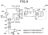
- the wireless power transmission system in Fig. 9 has the same structure as in Fig. 1 and also includes the power receiver sensing circuit 150 which works to measure a decrease in coil current to detect the presence or absence of the power receiver 200.
- the power receiver sensing circuit 150 includes the current measuring circuit 152, the rectifier circuit 154, the low-pass filter (LPF) 156, and the comparator 158.
- the current measuring circuit 152 works to measure an ac coil current ( I ) that is an ac electric current flowing through one of two conductors connecting between the alternating-current source 130 and the primary resonant circuit 110Convert the coil current ( I ) into an ac voltage ( V ) (which will also be referred to as a detection voltage), and output the ac voltage ( V ).
- the current measuring circuit 152 may alternatively be designed to measure electric current flowing through the other conductor connecting between the alternating-current source 130 and the primary resonant circuit 110.
- the rectifier circuit 154 works to rectify the ac voltage ( V ).
- the low-pass filter 156 works to remove high-frequency components from the rectified ac volage ( V ).
- the comparator 158 outputs the detection signal Sd of a H- level indicating the presence of a power receiver when the power receiver 200 that is a target to which electric power is required to be transferred exists, and the detection volage (i.e., the ac voltage ( V )) is higher than a threshold voltage Vth, in other words, the coil current is high.
- the comparator 158 outputs the detection signal Sd of a L -level indicating the absence of the power receiver.
- the comparator 158 may alternatively designed to have input terminals changed for each other, so that the detection signal Sd has the high level indicting the absence of the power receiver 200 or the low level indicating the presence of the power receiver 200.
- the wireless power transmission system actuates the alternating-current source 130 to apply ac power from the alternating-current source 130 to the primary resonant circuit 110. This achieves the high efficiency in transferring electric power from the power transmitter 100 to the power receiver 200.
- the wireless power transmission system deactivates the alternating-current source 130 to deliver no ac power from the alternating-current source 130 to the primary resonant circuit 110. This minimizes a useless supply of electric power from the alternating-current source 130 to the primary resonant circuit 110, thereby reducing leakage of magnetic flux generated in the primary coil 112.
- the power receiver sensing circuit 150 is, as described above, designed to detect a drop in coil current, but however, may alternatively be configured to detect a reduction in magnetic flux generated in the primary coil 112 which arises from a drop in coil current.
- the reduction in magnetic flux in the primary coil 112 may be sensed by a magnetic flux sensing circuit using a magnetic sensor or an inductive current sensing circuit using a coil instead of the current measuring circuit 152.
- the fourth embodiment is, as described above, designed to have the same structure as in the first embodiment (see Fig. 1 ), but however, may alternatively be configured to have the same structure as in the third embodiment (see Fig. 6 ).
- the tertiary coil 312 When the tertiary coil 312 is arranged on the side of the primary coil 112 in the structure in Fig. 1 (see Fig. 1 ), the absence of the secondary coil 212, as described in the second embodiment, will result in an increase in input impedance Zin expressed by Eq. (9), thereby decreasing electrical current flowing through the primary coil 112. Such current continues to flow as standby current through the primary coil 112. Such a standby current I1ds may be expressed by Eq. (14) below.
- I 1 s r 3 + j ⁇ 0 ⁇ L 3 ⁇ 1 ⁇ 0 ⁇ C 3 r 1 + j ⁇ 0 ⁇ L 1 ⁇ 1 ⁇ 0 ⁇ C 1 r 3 + j ⁇ 0 ⁇ L 3 ⁇ 1 ⁇ 0 ⁇ C 3 + ⁇ 0 2 ⁇ M 13 2 V 1
- the standby current I1s may be several amperes depending upon values of circuit constants of the primary resonant circuit 110 and the tertiary resonant circuit included in Eq. (14) above, which results in a useless loss of electric power to cause leakage of magnetic flux to occur in the primary coil 112.
- the standby current I3s expressed by Eq. (15) below also continues to flow through the tertiary coil 312.
- the standby current I3s causes the leakage of magnetic flux to occur in the tertiary coil 312.
- I 3 s j ⁇ 0 ⁇ M 12 r 1 + j ⁇ 0 ⁇ L 1 ⁇ 1 ⁇ 0 ⁇ C 1 r 3 + j ⁇ 0 ⁇ L 3 ⁇ 1 ⁇ 0 ⁇ C 3 + ⁇ 0 2 ⁇ M 13 2
- the capacitances of the primary capacitor 114 and the tertiary capacitor 314 may be set to values lower than those given by Eqs. (1) and (2). This increases the value of the input impedance Zin to decrease the standby current I1s expressed by Eq. (14) and the standby current I3s expressed by Eq. (15).
- the wireless power transmission system illustrated in Fig. 10 is equipped with the primary resonant circuit 110C and the tertiary resonant circuit 310C instead of the primary resonant circuit 110 and the tertiary resonant circuit 310 shown in Fig. 1 and also includes the power receiver detecting circuit 150C.
- the primary resonant circuit 110C includes the primary capacitor 114C instead of the primary capacitor 114 (see Fig. 1 ).
- the primary capacitor 114C is made of a variable capacitor designed to have a variable capacitance.
- the primary capacitor 114C is made of a unit consisting of the first capacitor 114l, the bidirectional switch SW1 connected in series with the first capacitor 114l, and the second capacitor 114s arranged in parallel to the first capacitor 114l and the bidirectional switch SW1.
- the second capacitor 114s has the capacitance Cs1 lower than the capacitance Cl1 of the first capacitor 114l.
- the first capacitor 114l connects with the second capacitor 114s in parallel thereto when the bidirectional switch SW1 is turned on or alternatively disconnects from the second capacitor 114l when the bidirectional switch SW1 is turned off.
- the capacitance C1c of the primary capacitor 114C will, therefore, be the capacitance Cs1 of the second capacitor 114s when the bidirectional switch SW1 is in the off-state or alternatively be the sum of the capacitance Cl1 of the first capacitor 114l and the capacitance Cs1 of the second capacitor 114s when the bidirectional switch SW1 is in the on-state (i.e., Cl1 + Cs1).
- the tertiary resonant circuit 310C includes the tertiary capacitor 314C instead of the tertiary capacitor 314 (see Fig. 1 ).
- the tertiary capacitor 314C is made of a variable capacitor having a variable capacitance.
- the tertiary capacitor 314C is made of a unit consisting of the first capacitor 314l, the bidirectional switch SW3 connects with the first capacitor 314l in series therewith, and the second capacitor 314s arranged in parallel to the first capacitor 314l and the bidirectional switch SW3.
- the capacitance Cs3 of the second capacitor 314s is lower than the capacitance Cl3 of the first capacitor 314l.
- the first capacitor 314l connects with the second capacitor 314s in parallel therewith when the bidirectional switch SW3 is turned on or alternatively disconnects from the second capacitor 314s when the bidirectional switch SW3 is turned off.
- the capacitance C3c of the tertiary capacitor 314C will, therefore, be the capacitance Cs3 of the second capacitor 314s when the bidirectional switch SW3 is in the off-state or alternatively be the sum of the capacitance Cl3 of the first capacitor 314l and the capacitance Cs3 of the second capacitor 314s when the bidirectional switch SW3 is in the on-state (i.e., Cl3 + Cs3).
- the capacitance Cs1 of the second capacitor 14s of the primary capacitor 114C and the capacitance Cs3 of the second capacitor 314s of the tertiary capacitor 314C may only need to be low values which set the standby current I1s in Eq. (14) and the standby current I3s in Eq. (15) to required values.
- the capacitance Cl1 of the first capacitor 114l of the primary capacitor 114C may only need to be determined so that a value of [Cl1 + Cs1] is equal to the capacitance C1 given by Eq. (1).
- the capacitance Cl3 of the first capacitor 314l of the tertiary capacitor 314C may only need to be determined so that a value of [Cl3 + Cs3] is equal to the capacitance C3 given by Eq. (2).
- the power receiver detecting circuit 150C is equipped with the delay circuit 159 which works to delay the detection signal Sd in time which is outputted from the comparator 158.
- the detection signal Sd which is outputted from the comparator 158 is inputted in the form of a switching signal to the bidirectional switch SW1 of the primary capacitor 114C.
- the detection signal Sd which is delayed in time is inputted in the form of a switching signal to the bidirectional switch SW3 of the tertiary capacitor 314C.
- the detection signal Sd is changed to the H-level to turn on the bidirectional switches SW1 and SW3, thereby causing the capacitance C1c of the primary capacitor 114C to be set to the capacitance C1 given by Eq. (1) and the capacitance C3c of the tertiary capacitor 314C to be set to the capacitance C3 given by Eq. (2).
- the detection signal Sd is changed to the L-level to turn off the bidirectional switches SW1 and SW3, thereby causing the capacitance C1c of the primary capacitor 114C to be set to the capacitance Cs1 which is lower than the capacitance C1 and the capacitance C3c of the tertiary capacitor 314C to be set to the capacitance Cs3 which is lower than the capacitance C3.
- This decreases the standby current I1 in Eq. (14) and the standby current I3 in Eq. (15), thereby minimizing an undesirable loss of electric power arising from flow of a large amount of the standby current I1s.
- the control of operation of the alternating-current source 130 which has been described in the fourth embodiment may be omitted. This embodiment is also capable of decreasing a leakage of magnetic flux arising from the flow of the standby currents I1s and I3s.
- the power receiver detecting circuit 150C serves as a capacitance controller to change the capacitances of the primary capacitor 114C and the tertiary capacitor 314C.
- the capacitance C1c of the primary capacitor 114C in the power-feeding mode may be set to a relatively low value because it, as can be seen in Eq. (1), needs to resonate with the self-inductance of the primary coil 112. Accordingly, each of the capacitance Cl1 of the first capacitor 14l and the capacitance Cs1 of the second capacitor 114s used in the primary capacitor 114C may be set to a relatively low value, thereby enabling such capacitors to be reduced in size. The same is true for the capacitance of the tertiary capacitor 314.
- the capacitance C1c of the primary capacitor 114C, the capacitance C2 of the secondary capacitor 214, and the capacitance C3c of the tertiary capacitor 314C may be determined according to Eqs. ( Rf1 ), ( Rf2 ), and (Rf3) below which are well known in the art.
- C 1 1 ⁇ 0 2 ⁇ L 1 1 ⁇ k 13 k 32 k 12
- C 2 1 ⁇ 0 2 ⁇ L 2 1 ⁇ k 32 k 13 k 12
- C 3 1 ⁇ 0 2 ⁇ L 3
- Eq. (Rf1) the calculation of the capacitance C1c of the primary capacitor 114C is achieved by multiplying a value in a denominator by (1-k13 ⁇ k12 / k32) derived using a coupling coefficient, thus resulting in the value of the capacitance C1c greater than that derived using Eq. (1).
- a target value of the capacitance of a capacitor required to decrease electrical current flowing through the primary coil 112 to a selected value is constant.
- a range of change in capacitance C1c required to decrease the above electrical current to a given value in the non-power feeding mode may, therefore, be decreased to be smaller when the capacitance C1c is set to a small value using Eq. (1) than that when the capacitance C1c is set to a great value using Eq. (Rf1). For this reason, this embodiment uses Eq. (1) to determine the capacitance C1c, thereby enabling the primary capacitor 114C working as a variable capacitor to be reduced in size.
- the capacitance C3c of the tertiary capacitor 314C is changed is because the current flowing through the primary coil 112 has been decreased at a time when the detection signal Sd is changed to the L-level, so that switching of the bidirectional switch SW1 of the primary capacitor 114C at that time will result in a decreased risk that a high level of surge voltage may be generated by the switching of the bidirectional switch SW1, and the current flowing through the tertiary coil 312 usually decreases with a decrease in the capacitance C1c of the primary capacitor 114C, so that the switching of the bidirectional switch SW3 of the tertiary capacitor 314C will also result in a decreased risk that a high level of surge voltage may be generated by the switching of the bidirectional switch SW1.
- the delay circuit 159 may be omitted.
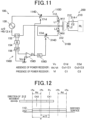
- the wireless power transmission system illustrated in Fig. 11 includes the primary resonant circuit 110D and the tertiary resonant circuit 310D instead of the primary resonant circuit 110C and the tertiary resonant circuit 310C illustrated in Fig. 10 and also includes the power receiver detecting circuit 150D instead of the power receiver detecting circuit 150C illustrated in Fig. 10 .
- the primary resonant circuit 110D uses the primary capacitor 114D that is a variable capacitor to variably change the capacitance C1d as a function of a control input in the form of the control voltage Vc.
- the tertiary resonant circuit 310D uses the tertiary capacitor 314D that is a typical variable capacitor to vary the capacitance C3d as a function of the control voltage Vc.
- the power receiver sensing circuit 150D is equipped with the voltage conversion circuit 158D in connection with the primary capacitor 114D and the tertiary capacitor 314D.
- the voltage conversion circuit 158D is used as the comparator 158 of the power receiver sensing circuit 150C in the structure illustrated in Fig. 10 .
- the voltage conversion circuit 158D is made of a differential amplifier circuit working to output the control voltage Vc as a function of a difference between the above-described detection voltage and the reference voltage Vrc.
- the delay circuit 159D is also provided which is used as the delay circuit 159 in the structure of Fig. 10 .
- the delay circuit 159D works to delay the variable control voltage Vc in time.
- variable capacitors used as the primary capacitor 114D and the tertiary capacitor 314D are designed to have capacitances decreasing with an elevation in level of the control voltage Vc.
- the voltage conversion circuit 158D is made of a differential amplifier circuit configured to have input of the detection voltage to an inverting input terminal (-) thereof and output the control voltage Vc which decreases with an elevation in level of the detection voltage derived by the current measuring circuit 152.
- the variable capacitors i.e., the primary capacitor 114D and the tertiary capacitor 314D
- the voltage conversion circuit 158D is designed to have the detection voltage inputted to a non-inverting input terminal (+) thereof.
- the wireless power transmission system in Fig. 11 operates in the same way as in the first embodiment in the power feeding mode.
- the wireless power transmission system is also capable of reducing a loss of electric power arising from flow of a large amount of the standby current I1s in the non-power feeding mode.
- the control of operation of the alternating-current source 130 described in the fourth embodiment may be omitted.
- the risk that the leakage of magnetic flux may result from flow of the standby currents I1s and I3s may be eliminated.
- the capacitance C1d of the primary capacitor 114D in the power feeding mode may be determined, like the capacitance C1c of the primary capacitor 114c, to be relatively low. This reduces a range of change in the capacitance C1 in either of the power feeding mode and the non-power feeding mode, thereby facilitating use of a variable capacitor as the primary capacitor 114D which has a capacitance variable as a function of the control input (i.e., the control valve Vc).
- the power receiver sensing circuit 150D works as a capacitance controller to change the capacitances of the primary capacitor 114D and the tertiary capacitor 314D.
- the primary capacitors 114C and 114D of the primary resonant circuits 110C and 110D and the tertiary capacitors 314C and 314D of the tertiary resonant circuits 310C and 310D are, as described above, made of variable capacitors, but however, only each of the tertiary resonant circuits 310C and 310D may alternatively be made of a non-variable capacitor having a constant capacitance. In this structure, it is impossible to control the leakage of magnetic flux arising from the standby current I3s, but however, it is possible to minimize a loss of electric power and leakage of magnetic flux resulting from flow of the standby current I1s.
- the above-described fifth embodiment is a modification of the structure in the first embodiment (see Fig. 1 ), but however, may alternatively designed to have a modified structure in the third embodiment (see Fig. 6 ).
- the determination of circuit constants of each circuit installed in the wireless power transmission system is usually achieved based in a design condition where the primary coil 112 and the secondary coil 212 face each other (see Figs. 1 and 6 ), specifically, the primary coil 112 and the secondary coil 212 are oriented to have central axes thereof aligned with each other.
- the determination of the capacitance of the secondary capacitor 214 to provide an enhanced power factor of ac power described in the first and third embodiments is preferably achieved in a design condition which will be described below in detail.
- the following discussion on an example illustrated in Fig. 12 assumes that the secondary coil 212 moves closer to and then away from the primary coil 112.
- a design condition may be considered in which the center axis CX2 of the secondary coil 212 is located in one of regions Rd defined between a position -Ph and a coil end position -Pe and between a position +Ph and a coil end position +Pe in a direction in which the secondary coil 212 moves.
- the coil ends -Pe and +Pe represent ends of the primary coil 112 which are opposed to each other in the direction of movement of the secondary coil 212.
- Each of the positions -Ph and +Ph is a position which is one-half of an interval between the center position Pc (i.e., position of the center axis CX1 ) of the primary coil 112 and a corresponding one of the coil ends -Pe and +Pe away from a corresponding one of the coil ends -Pe and +Pe in the direction of movement of the secondary coil 212.
- Such a design condition will also be referred to as a first design condition below.
- FIG. 13 Another design condition demonstrated in Fig. 13 may be considered in which the center (i.e., the center axis) of the secondary coil 212 is arranged on one of regions Rd between the center position Pc (i.e., position of the center axis CX1 ) of the primary coil 112 and the position -Ph and between the center position Pc and the position +Ph in the direction in which the secondary coil 212 moves.
- Each of the positions -Ph and +Ph is, as described above, a position which is one-half of an interval between the center position Pc of the primary coil 112 and a corresponding one of the coil ends -Pe and + Pe away from the center position Pc in the direction of movement of the secondary coil 212.
- Such a design condition will also be referred to as a second design condition below.
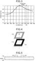
- Fig. 14 represents a comparison between power factors in a second setting example in the second design condition and in a first setting example in the first design condition.
- the first setting example is an example of the first design condition where an intermediate position between the coil end -Pe of the primary coil 112 and the 1/2 position -Ph coincides with the center position of the secondary coil 212.
- the second setting example is an example of the second design condition where the center position Pc of the primary coil 112 coincides with the center position of the secondary coil 212.
- the power factor decreases as the center position of the secondary coil 212 moves away from a design point, that is, the center position Pc of the primary coil 112.
- the power factor slightly drops near the center position Pc of the primary coil 112, but is substantially kept constant over a wide range. It, therefore, follows that in order to ensure a high level of the power factor over an increased range in addition to a condition where the major surface of the primary coil 112 faces that of the secondary coil 212, the wireless power transmission system is preferably designed to satisfy the first design condition.
- the wireless power transmission system is preferably configured to meet the second design condition, not the first design condition. If the wireless power transmission system is designed to meet the first design condition, electric powers transferred from the first coil and the second coil that are ones of the primary coils 112, as demonstrated in Fig. 15 , may overlap each other in a region around adjacent ends + Pe and - Pe of the first and second coils, thereby resulting in an increase in pulsation of the electric powers. In contrast, if the wireless power transmission system is designed to meet the second design condition, it, as can be seen in Fig. 16 , results in a decreased overlap between electric powers delivered from the first and second coils located adjacent to each other, thus reducing the pulsation of the electric powers.
- the wireless power transmission system in each of the above embodiments is equipped with a single pair of the primary resonant circuit and the tertiary resonant circuit, but however, may alternatively be designed to have a plurality of power transmitting units each of which includes a single pair of a primary resonant circuit and a tertiary resonant circuit in the way as described below.
- the wireless power transmission system may be designed to have a structure, as illustrated in Fig. 17 , for use in automotive vehicles.
- the wireless power transmission system in Fig. 17 is equipped with a plurality of power transmitting units each of which includes the primary resonant circuit 110, the tertiary resonant circuit 310, and the power receiver sensing circuit 150 illustrated in Fig. 9 .
- the wireless power transmission system in Fig. 17 is configured as a power feeding system which works to transfer electric power from the power transmitter 100E disposed on or in a lane of the vehicle traffic road RS to the power receiver 200 (see Fig. 9 ) installed in the vehicle VH .
- the vehicle VH is implemented by an electric vehicle or a hybrid vehicle using electric power as traction power.
- Fig. 17 is implemented by an electric vehicle or a hybrid vehicle using electric power as traction power.
- the x-axis indicates a direction of forward movement of the vehicle VH along the lane of the vehicle traffic road RS .
- the y -axis indicates a width direction of the vehicle traffic road RS .
- the z -axis indicates a vertical direction. The same definition of the x -, y-, and z -axes applies to the following drawings.
- the power transmitter 100E is equipped with a plurality of power transmitting units each of which includes the primary resonant circuit 110, the tertiary resonant circuit 310, and the power receiver sensing circuit 150 illustrated in Fig. 9 .
- the power transmitter 100E also includes the alternating-current source 130E.
- the alternating-current source 130E includes the power circuit 132 and a plurality of power transmission output circuits 134 which apply electric power to the primary resonant circuits 110.
- the primary coils 112 (see Fig. 9 ) of the primary resonant circuits 110 are arranged away from each other along the lane of the vehicle traffic road RS .
- the tertiary coil 312 of each of the tertiary resonant circuits 310 is stacked on a corresponding one of the primary coils 112 (see Figs. 4 and5).
- the power circuit 132 works to convert ac power delivered from an external power supply into dc power.
- Each of the power transmission output circuits 134 includes an inverter which converts the dc power supplied from the power circuit 132 into ac power at the operating frequency.
- Each of the power transmission output circuits 134 is controlled in operation by a corresponding one of the power receiver sensing circuits 150.
- the power receiver 200 mounted in the vehicle VH includes the secondary resonant circuit 210, the power receiving circuit 220, and the battery 230 (see Fig. 9 ).
- the secondary coil 212 of the secondary resonant circuit 210 is arranged on the bottom of the vehicle VH , so that it may face the primary coil 112 of one of the primary resonant circuits (see Fig. 4 ).
- the electric power induced in the secondary resonant circuit 210 is used to charge the batter 230 through the power receiving circuit 220 for driving an electric motor, not shown.
- Each of the power receiver sensing circuits 150 works to detect the presence of the secondary coil 212 to which it is required to transfer electric power from the primary coil 112, in other words, the presence of the vehicle VH in which the power receiver 200 is mounted.
- each of the power receiver sensing circuits 150 actuates a corresponding one of the power transmission output circuits 134 to apply electric power to a corresponding one of the primary resonant circuits 110 to transfer the electrical energy to the power receiver 200 of the vehicle VH .
- each of the power receiver sensing circuits 150 deactivates a corresponding one of the power transmission output circuits 134.
- the wireless power transmission system in this embodiment offers substantially the same beneficial advantages as in the above embodiments.
- the power receiver sensing circuits 150 may be omitted, and the power transmission output circuits 134 may be kept on at all times.
- the input impedance Zin of the primary resonant circuit 100 is, as described in the second embodiment, increased, thus resulting in an increase in drop in current flowing through the primary resonant circuit 110 in the absence of the secondary coil 212, the power receiver sensing circuits 150 may be omitted.
- the wireless power transmission system may be designed to a single power transmission output circuit 134.
- the wireless power transmission system may be designed for the vehicle VH to have a structure illustrated in Fig. 18 which is equipped with a plurality of power transmitting units each of which includes the primary resonant circuit 110C, the tertiary resonant circuit 310C, and the power receiver sensing circuit 150C illustrated in Fig. 10 .
- the wireless power transmission system in Fig. 18 is configured as a power feeding system which works to transfer electric power from the power transmitter 100F disposed on or in the lane of the vehicle traffic road RS to the power receiver 200 (see Fig. 10 ) installed in the vehicle VH .
- the power transmitter 100F is equipped with a plurality of power transmitting units each of which includes the primary resonant circuit 110C, the tertiary resonant circuit 310C, and the power receiver sensing circuit 150C illustrated in Fig. 10 .
- the power transmitter 100F is equipped with the alternating-current source 130F.
- the alternating-current source 130F is, unlike the alternating-current source 130E in Fig. 17 , equipped with a single power transmission output circuit 134.
- the primary coils 112 (see Fig. 10 ) of the primary resonant circuits 110C are, like the primary resonant circuits 110 in Fig. 17 , arranged away from each other along the lane of the vehicle traffic road RS.
- the tertiary coil 312 of each of the tertiary resonant circuits 310C is, like the tertiary resonant circuits 310 in Fig. 17 , stacked on a corresponding one of the primary coils 112 (see Figs. 4 and5).
- the structure of the power receiver 200 installed in the vehicle VH is the same as in the wireless power transmission system illustrated in Fig. 17 .
- Each of the power receiver sensing circuits 150C works to detect the presence of the secondary coil 212 to which it is required to transfer electric power from the primary coil 112, in other words, the presence of the vehicle VH in which the power receiver 200 is mounted.
- each of the power receiver sensing circuits 150C changes the capacitance of the primary capacitor 114C of a corresponding one of the primary resonant circuits 110C to a capacitance used in the power feeding mode.
- the power transmission output circuit 134 then applies electric power to the primary resonant circuit 110C equipped with the primary capacitor 114C whose capacitance has been changed to that used in the power feeding mode, thereby transferring electrical energy to the power receiver 200 installed in the vehicle VH .
- each of the power receiver sensing circuits 150C changes the capacitance of the primary capacitor 114C of a corresponding one of the primary resonant circuits 110C to a capacitance used in the non-power feeding mode.
- the wireless power transmission system works to supply current only to the primary resonant circuit 110C equipped with the primary capacitor 114C regulated to have the capacitance set for use in the power feeding mode without supplying current to the primary resonant circuits 110C equipped with the primary capacitors 114C regulated to have the capacitances set for use in the non-power feeding mode. This minimizes a useless loss of electric power.
- the wireless power transmission system in this embodiment is designed to use the single power transmission output circuit 134 to operate the plurality of primary resonant circuits 110C.
- the wireless power transmission system in this embodiment offers substantially the same beneficial advantages as in the above embodiments.
- the wireless power transmission system for vehicles may be designed to include a plurality of primary resonant circuits 110D, a plurality of tertiary resonant circuits 310D, and a plurality of power receiver sensing circuits 150D.
- Figs. 17 and 18 are designed to use the structure in the first embodiment (see Fig. 1 ), but however, may alternatively be constructed to use the structure in the third embodiment (see Fig. 6 ).
- the above-described the wireless power transmission system designed for vehicles which includes the power transmitting units each of which the primary resonant circuit and the tertiary resonant circuit offers substantially the same beneficial advantages as those in the above embodiments.
Abstract
A wireless power transmission system is provided which wirelessly transfer electric power from a power transmitter to a power receiver. The wireless power transmission system works to set a capacitance of a primary capacitor of a primary resonant circuit to undergo resonance with a self-inductance of a primary coil at an angular frequency that is an operating frequency. A tertiary capacitor of a tertiary resonant circuit has a capacitance set to undergo resonance with a self-inductance of a tertiary coil. A secondary capacitor of a secondary resonant circuit has a capacitance set to reduce a reactive component of ac power arising from self-inductances and mutual inductances of the primary coil, the secondary coil, and the tertiary coil.
Description
- The present application claims the benefit of priority of
Japanese Patent Application No. 2021-028217 filed on February 25, 2021 2022-008670 filed on January 24, 2022 - This disclosure relates generally to a wireless power transmission system.
- There is proposed a wireless power transmission system which wirelessly delivers electric power from a power transmitter serving as a primary unit to a power receiver serving as a secondary unit. For instance, Japanese translation of PCT application publication No. 2002-508916 discloses an inductive power transfer system which works to transfer electric power from a primary inductive conductor (i.e., primary coil) to a secondary resonance pickup circuit through an intermediate resonance loop which resonates at a system frequency.
- When a capacitance of a capacitor mounted in each of a plurality of resonant circuits installed in a wireless power transmission system working to transfer electric power from a primary resonant circuit that is one of the resonant circuits to a secondary resonant circuit that is one of the resonant circuits is, like prior art systems, selected to resonate with a self-inductance of a corresponding one of the resonant circuits at a frequency of induced electric power, it leads to a risk that a power factor of the induced electric power may decrease. Such a decrease in power factor will undesirably lead to an increase in loss of electrical energy outputted to the primary resonant circuit. This drawback becomes significant as a coupling coefficient between the coil of the primary resonant circuit and the coil of the secondary resonant circuit becomes high.
- This disclosure was made in order to solve at least one of the above problems and may be realized as the following modes or examples of application.
- According to one aspect of this disclosure, there is provided a wireless power transmission system which works to supply electric power wirelessly from a power transmitter to a power receiver. The wireless power transmission system comprises: (a) a power transmitter which includes a primary resonant circuit and an alternating-current source, the primary resonant circuit including a primary coil and a primary capacitor for use in power transmission, the alternating-current source working to apply ac power at a given operating frequency to the primary resonant circuit; (b) a power receiver which includes a secondary resonant circuit, the secondary resonant circuit including a secondary coil and a secondary capacitor for use in a power reception, the secondary coil being to be magnetically coupled with the primary coil; and (c) a tertiary resonant circuit which includes a tertiary coil and a tertiary capacitor. The tertiary coil is arranged to achieve magnetic coupling with the primary coil and the secondary coil. The tertiary capacitor constitutes a short-circuit resonant circuit along with the tertiary coil. The primary coil has a self-inductance L1. A capacitance of the primary capacitor is set to a capacitance C1, as given by Eq. (1) below, to cause resonance in the primary capacitor and the primary coil at an angular frequency ω0 that is the operating frequency.

- The tertiary coil has a self-inductance L3. A capacitance of the tertiary capacitor is set to a capacitance C3, as given by Eq. (2) below, to cause resonance in the tertiary capacitor and the tertiary coil at the operating frequency.

- A capacitance of the secondary capacitor is determined to decrease a reactive component of the ac power which arises from the self-inductances and mutual inductances of the primary coil, the secondary coil, and the tertiary coil.
- When electrical energy is transferred from the power transmitter to the power receiver, the wireless power transmission system is capable of decreasing a reactive component of ac power applied from the alternating-current source to the primary resonant circuit, thereby minimizing a drop in power factor of the ac power supplied to the primary resonant circuit. This reduces a loss of energy in the alternating-current source. For instance, in a case where the alternating-current source is equipped with an inverter and a filter, an energy loss is reduced in the inverter and the filter. The above structure of the wireless power transmission system is also capable of determining the capacitance of the primary capacitor of the primary resonant circuit and the capacitance of the tertiary capacitor of the tertiary resonant circuit regardless of coupling coefficients of the primary coil, the secondary coil, and the tertiary coil, thereby resulting in an increase in available types of the power receiver to which electrical energy is transferred from the power transmitter
- The present disclosure will be understood more fully from the detailed description given hereinbelow and from the accompanying drawings of the preferred embodiments of the invention.
- In the drawings:
-
Fig. 1 is a schematic view which illustrates a structure of a wireless power transmission system according to the first embodiment; -
Fig. 2 is an explanatory view which represents a relation between a resistive load (i.e., a load resistance) and a power factor in the first embodiment; -
Fig. 3 is an explanatory view which represents a relation between a deviation or error from a capacitance of a secondary capacitor and a power factor; -
Fig. 4 is an explanatory view which demonstrates layout of a primary coil and a tertiary coil in the second embodiment; -
Fig. 5 is an explanatory view which illustrates structures of a primary coil and a tertiary coil formed integrally with each other; -
Fig. 6 is a schematic view which illustrates a structure of a wireless power transmission system in the third embodiment; -
Fig. 7 is an explanatory view which represents a resistive load and a power factor in the third embodiment; -
Fig. 8A is an explanatory view which represents a relation between a deviation from a capacitance of a secondary capacitor and a power factor; -
Fig. 8B is an explanatory view which represents relations between a capacitance of a tertiary capacitor and an electrical current flowing through a primary coil in two different types of structure; -
Fig. 9 is a schematic view which illustrates a structure of a wireless power transmission system in the fourth embodiment; -
Fig. 10 is a schematic view which illustrates a structure of a wireless power transmission system in the fifth embodiment; -
Fig. 11 is a schematic view which illustrates a modified structure of a wireless power transmission system in the fifth embodiment; -
Fig. 12 is an explanatory view which represents a first design condition for use in determining circuit constants in a wireless power transmission system; -
Fig. 13 is an explanatory view which represents a second design condition for use in determining circuit constants in a wireless power transmission system; -
Fig. 14 is an explanatory view which represents relations between design conditions and power factors; -
Fig. 15 is an explanatory view which demonstrates a pulsation of electric power in a first design condition; -
Fig. 16 is an explanatory view which demonstrates a pulsation of electric power in a second design condition; -
Fig. 17 is a schematic view which illustrates a structure of a wireless power transmission system designed for use in automotive vehicles; and -
Fig. 18 is a schematic view which illustrates another structure of a wireless power transmission system designed for use in automotive vehicles. - A wireless power transmission system in the first embodiment, as illustrated in
Fig. 1 , includes thepower transmitter 100, thepower receiver 200, and the tertiaryresonant circuit 310. Thepower receiver 200 receives electric power wirelessly delivered from thepower transmitter 100. - The
power transmitter 100 includes the primaryresonant circuit 110 and the alternating-current source 130. Theprimary resonant circuit 110 is an electrical circuit working to supply electric power to thepower receiver 200 using electromagnetic induction due to resonance. Specifically, the primaryresonant circuit 110 includes theprimary coil 112 and theprimary capacitor 114 connected directly to theprimary coil 112. Theprimary capacitor 114 functions as a resonant capacitor to resonate electric power applied to theprimary coil 112. The alternating-current source 130 is a device working to apply an ac power at a preselected operating frequency f0 (i.e., angular frequency ω0) to the primaryresonant circuit 110. The alternating-current source 130 includes a power supply device which converts an ac power produced by an external power supply into a dc power and an inverter which works to convert the dc power delivered from the power supply device into an ac power at an operating frequency. The alternating-current source 130 may also include a filter following the inverter in the signal path. - The
power receiver 200 may be installed in a variety of devices, such as electronic devices or electric automobiles, which are operated using electric power. Thepower receiver 200 includes the secondaryresonant circuit 210, thepower receiving circuit 220, and thebattery 230. The secondaryresonant circuit 210, like the primaryresonant circuit 110, includes thesecondary coil 212 and the secondary capacitor 214 which is connected in series with thesecondary coil 212 and serves as a resonant capacitor. The secondaryresonant circuit 210 is a circuit which obtains ac power, as induced in thesecondary coil 212, when thesecondary coil 212 and theprimary coil 112 are in magnetic resonant coupling with each other. - The
power receiving circuit 220 is a device working to convert ac power, as derived in the secondaryresonant circuit 210, into dc power to charge thebattery 230. The electrical energy stored in thebattery 230 is used as electric power in a device in which thepower receiver 200 is installed. In other words, each of thepower receiving circuit 220 and thebattery 230 functions as an electrical load in the secondaryresonant circuit 210. In the following discussion, thepower receiving circuit 220 and thebattery 230 will also be referred to as the resistive load RL. - The tertiary
resonant circuit 310 is designed as a closed circuit made up of thetertiary coil 312 and thetertiary capacitor 314 serving as a resonant capacitor. - When it is required to transfer electric power from the
power transmitter 100 to thepower receiver 200, the secondaryresonant circuit 210 is arranged to place thesecondary coil 212 in magnetic coupling with theprimary coil 112 of the primaryresonant circuit 110. The tertiaryresonant circuit 310 is also arranged to place thetertiary coil 312 in magnetic coupling with theprimary coil 112 and thesecondary coil 212.Fig. 1 indicates the magnetic coupling of thecoils coil 212 using two parallel straight lines. - The
primary coil 12 of the primaryresonant circuit 110 has the self-inductance L1. Theprimary capacitor 114 has the capacitance C1 given by the following Eq. (1) to undergo resonance with theprimary coil 112 at the angular frequency ω0 that is the operatingfrequency f0. 
- The
tertiary coil 312 of the tertiaryresonant circuit 310 has the self-inductance L3. Thetertiary capacitor 314 has the capacitance C3 given by the following Eq. (2) to undergo resonance with thetertiary coil 312 at the angularfrequency ω0. 
- The
secondary coil 212 of the secondaryresonant circuit 210 has the self-inductance L2. The secondary capacitor 214 is preferably designed to have a capacitance higher than the capacitance C2r given by the following Eq. (3). Specifically, it is advisable that the secondary capacitor 214 have the capacitance C2 defined by the following Eq. (4). Note that the capacitance C2r is a value selected to resonate the secondary capacitor 214 and thesecondary coil 212 at the angular frequency ω0.


- The coupling coefficient knm in the absence of magnetic coupling between the coils will be zero. This results in the mutual inductance Mnm being zero. For instance, in the absence of the
power receiver 200, the coupling coefficient k12 of theprimary coil 112 and thesecondary coil 212 will be zero. The mutual inductance M12 of theprimary coil 112 and thesecondary coil 212 will be zero. - Note that the mutual inductances M12, M13, and M32 used to set the capacitance of the secondary capacitor 214 to the capacitance C2 given by Eq. (4) above are given by values derived using the coupling coefficients k12, k13, and k32 as a function of positional relation among the coils.
- The input impedance Zin from the alternating-
current source 130 to the primaryresonant circuit 110 is defined by Eq. (7) below using circuit equations of the primaryresonant circuit 110, the secondaryresonant circuit 210, and the tertiaryresonant circuit 310.
- Eq. (7) omits resistance components because the resistances r1, r2, and r3 in windings of the
primary coil 112, thesecondary coil 212, and thetertiary coil 312 are much lower than reactances [ω0·L1], [ω0·L2], and [ω0·L3] at the operating frequency f0. - The delivery of ac power, as inputted from the alternating-
current source 130 to the primaryresonant circuit 110, to the secondaryresonant circuit 210 at high efficiency requires decreasing an imaginary component in Eq. (7) to enhance the power factor of ac power. Ideally, the imaginary component is preferably set to zero. - Eq. (1) above is derived by setting the first term [jω0·L1+1/(jω0·C1)] in Eq. (7) to zero. The satisfaction of Eq. (1) enables circuit constants in the primary
resonant circuit 110 to be determined regardless of the degree of mutual coupling among theprimary coil 112, thesecondary coil 212, and thetertiary coil 312. - Eq. (4) above is derived by setting {(M13/M32) 2[jω0·L2+1/jω0·C2)]-2jω0·M12·M13/M32} in the second and third terms of Eq. (7) to zero.
- Eq. (2) above may be used, like the capacitance C1 in Eq. (1), to determine circuit constants in the tertiary
resonant circuit 310 regardless of the degree of mutual coupling among theprimary coil 112, thesecondary coil 212, and thetertiary coil 312. - Eq. (2) may be obtained in the following way. For instance, in the absence of the
power receiver 200 in a case where thetertiary coil 312 has a constant positional relation to theprimary coil 112, it is usually required to maximize the input impedance Zin against current from the alternating-current source 130 to the primaryresonant circuit 110 in order to eliminate an excess current input thereto. The input impedance Zin is expressed by Eq. (8) using circuit equations in the primaryresonant circuit 110 and the tertiaryresonant circuit 310.
- Eq. (8) omits resistance components for the same reasons as for Eq. (7).
- The input impedance Zin expressed by Eq. (8) is maximized when an imaginary component of a denominator in the fourth term, i.e., [jω0·L3+1/(jω0·C3)] is zero. Eq. (2) above may, therefore, be derived using a relation of [jω0·L3+1/(jω0·C3)]= 0.
- We conducted simulations about a relation between the resistive load RL and the power factor in the embodiment in which the capacitance of the secondary capacitor 214 is determined according to Eq. (4) above and a comparative example in which the capacitance of the secondary capacitor 214 is determined according to Eq. (3) above. Results of the simulations are shown in
Fig. 2 . Note that the capacitance C1 of theprimary capacitor 114 and the capacitance C3 of thetertiary capacitor 314 are determined according to Eqs. (1) and (2). The graph inFig. 2 shows that in the comparative example, the power factor is less than one, which results from the effect of a reactive component of the ac power, and that the smaller the resistive load RL, in other words, the higher the load, the smaller the power factor. In contrast, the graph shows that in this embodiment, the power factor is kept constant to be one regardless of the value of the resistive load RL, which achieves the highest-efficiency in transferring the ac power. - We also conducted simulations about a relation between an error [%] that is a deviation from the capacitance C2 defined by Eq. (4) above and the power factor. Results of the simulations are illustrated in the graph of
Fig. 3 . The graph shows that a reduction in power factor may be minimized by decreasing a reactive component of ac power without having to set the capacitance of the secondary capacitor 214 to the capacitance C2 derived according to Eq. (4) above. For instance, the power factor may be improved to be 0.6 or more in a range of the error between -25% and +45%. The power may also be improved to be 0.8 or more in a range of the error between -15% and +25%. Note that the above values are round off to one decimal place. Negative value of the errors results in rate of a reduction in power factor lower than positive values of the errors. It is, thus, advisable that the error be in a range of 0% to +25%. - [M12·M21/M13] in Eq. (4) above usually has a positive value, thus causing the capacitance C2, as derived according to Eq. (4), to have a value greater than the capacitance C2r expressed by Eq. (3) above (i.e., C2 > C2r). The capacitance of the secondary capacitor 214 may be set to a value greater than the capacitance C2r given by Eq. (3) in order to reduce the reactive component of ac power to minimize the reduction in power factor. [M12·M32/M13] may have a negative value depending upon the degree of coupling among the coils. In such a case, the capacitance C2 defined by Eq. (4) will be smaller than the capacitance C2r defined by Eq. (3) (i.e., C2 < C2r). The capacitance of the secondary capacitor 214 may be set to a value smaller than the capacitance C2r given by Eq. (3) in order to decrease the reactive component of ac power to minimize the reduction in power factor.
- For the reasons described above, the capacitance of the secondary capacitor 214 may be determined to decrease the reactive component of the ac power, as arising from the self-inductances L1, L2, and L3 and the mutual inductances M12, M13, and M32 of the
primary coil 112, thesecondary coil 212, and thetertiary coil 312, to minimize the reduction in power factor. - As apparent from the above discussion, when it is required to transfer electricity from the
power transmitter 100 to thepower receiver 200, the structure in this embodiment is capable of minimizing the reduction in power factor of ac power delivered from the alternating-current source 130 to the primaryresonant circuit 110, thereby ensuring the high efficiency of transfer of power to thepower receiver 200. - The first embodiment is, as described above, designed to have the
secondary coil 212 of the secondaryresonant circuit 210 which is arranged in magnetic coupling with theprimary coil 112 of the primaryresonant circuit 110 and also have thetertiary coil 312 of the tertiaryresonant circuit 310 which is arranged in magnetic coupling with each of theprimary coil 112 and thesecondary coil 212. In other words, the first embodiment is configured not to specify the positional relation among theprimary coil 112, thesecondary coil 212, and thetertiary coil 312. The second embodiment is designed to specify a desirable relation in location among the above coils. - The
tertiary coil 312 is, as illustrated inFig. 4 , preferably stacked on the surface of theprimary coil 112 which faces away from thesecondary coil 212, in other words, is arranged on the opposite side of theprimary coil 112 to thesecondary coil 212. Although not illustrated in the drawings, thetertiary coil 312 may alternatively be stacked on the surface of theprimary coil 112 which directly faces thesecondary coil 212 or arranged adjacent to the side surface (i.e., the peripheral surface) of theprimary coil 112. In other words, it is advisable that thetertiary coil 312 be arranged closer to theprimary coil 112, i.e., thepower transmitter 312 than to thesecondary coil 212 or directly on theprimary coil 112 so as to achieve a constant coefficient k13 (also referred to as inductive coupling factor) of coupling with theprimary coil 112. The stacking of thetertiary coil 312 on theprimary coil 112 is easier to increase the coupling coefficient k13 than the arrangement of thetertiary coil 312 adjacent to theprimary coil 112. - The input impedance Zin given by Eq. (7) may be rewritten using Eqs. (1), (2), and (4) as being expressed according to Eq. (9) as a function of the resistive load RL.

- When the
tertiary coil 312 is, as described above, arranged close to or on theprimary coil 112, it will result in a constant positional relation between theprimary coil 112 and thetertiary coil 312, so that the coupling coefficient k13 will be kept constant. Alternatively, when a distance at which thesecondary coil 212 is away from theprimary coil 112 is increased, it will result in a decrease in coefficient k32 of coupling between thetertiary coil 312 and thesecondary coil 212. The input impedance Zin expressed by Eq. (9), thus, increases. Accordingly, when thesecondary coil 212 moves away from theprimary coil 112, and thepower transmitter 100 transfers no power to thepower receiver 200, a decrease in electric power delivered from the alternating-current source 130 to the primaryresonant circuit 110, i.e., electrical current flowing through the primary coil 112 (which will also be referred to as coil current) may be achieved by increasing the input impedance Zin. This results in a decrease in undesirable loss of electric power, which will reduce the leakage of magnetic flux generated in theprimary coil 112. - It is, as demonstrated in
Fig. 5 , preferable that theprimary coil 112 and thetertiary coil 312 are formed or fabricated integrally in the form of a multi-layered printed circuit board with theprimary capacitor 114 and thetertiary capacitor 314 mounted on a surface of the multi-layered printed circuit board. This structure enhances the coupling coefficient k13 of theprimary coil 112 and thetertiary coil 312 and the coupling coefficient k13. - The coefficient η of transmission of ac power from the
power transmitter 100 to thepower receiver 200 is given by the following Eq. (10) using circuit equations of the primaryresonant circuit 110, the secondaryresonant circuit 210, and the tertiaryresonant circuit 310.
- The transmission coefficient η expressed by Eq. (10) is maximized when the capacitance C2 of the secondary capacitor 214 is defined by Eq. (4) above. The optimum load RLopt is given by Eq. (11).

- By substituting Eq. (11) in Eq. (10) and rewriting it using knm (nm = 12, 13, 32) and Qi (= ω0 · Li / ri) (i = 1, 2, 3), the maximum coefficient ηmax is expressed by Eq. (12) below where ri is a resistance in a winding of an i th- order coil.

- Eq. (12) shows that the transmission coefficient may be enhanced by increasing the coupling coefficient k13 of the
primary coil 112 and thetertiary coil 312 or the coupling coefficient k32 of thetertiary coil 312 and thesecondary coil 212. For the reasons described above, it is advisable that the coupling coefficient k13 of theprimary coil 112 and thetertiary coil 312 be increased by forming theprimary coil 112 and thetertiary coil 312 integrally with a multi-layered printed circuit board. This improves the power transmission coefficient. Theprimary capacitor 114 and thetertiary capacitor 314 are preferably mounted on the same multi-layered printed circuit board as theprimary coil 112 and thetertiary coil 312, thereby minimizing parasitic inductances or capacitances which will exist between conductive wires on the multi-layered printed circuit board to reduce a deviation of the resonant frequency. - Instead of forming the
secondary coil 212 and thetertiary coil 312 integrally with each other using a printed circuit board, theprimary coil 112 and thetertiary coil 312 are preferably formed integrally with each other using a printed circuit board in favor of increasing the input impedance Zin in the absence of thepower receiver 200. - In the example illustrated in
Fig. 5 , the two-layered printed circuit board has a first and second major surfaces. Theprimary coil 112 is arranged on the first major surface, while thetertiary coil 312 is arranged on the second major surface. Theprimary coil 112 and thetertiary coil 312 may alternatively be formed integrally with each other using a three or more-layered printed circuit board. - The structure in the first embodiment illustrated in
Fig. 1 has the tertiaryresonant circuit 310 discrete from the primaryresonant circuit 110, while the structure in the third embodiment is, as illustrated inFig. 6 , designed to include the tertiaryresonant circuit 310B with thetertiary coil 312 connected directly to theprimary coil 112 of the primaryresonant circuit 110B. The tertiaryresonant circuit 310B has thetertiary capacitor 314 connected in parallel to thetertiary coil 312. - The
primary coil 112 of the primaryresonant circuit 110B has the self-inductance L1. The capacitance of theprimary capacitor 114 may be selected as the capacitance C1 given by Eq. (1) to resonate with theprimary coil 112 at the angular frequency ω0 of the operating frequency f0. This is for the same reasons as described in the first embodiment about the primaryresonant circuit 110. - The
tertiary coil 312 of the tertiaryresonant circuit 310B has the self-inductance L3. The capacitance of thetertiary capacitor 314 may be set to the capacitance C3 given by Eq. (2) to resonate thetertiary capacitor 314 and thetertiary coil 312 at the angular frequency ω0. This is also for the same reasons as described in the first embodiment about the tertiaryresonant circuit 310. - In the secondary
resonant circuit 210 in this embodiment, it is advisable, like in the first embodiment, that the capacitance of the secondary capacitor 214 be set to a value greater than the capacitance C2r defined by Eq. (3) in a condition where thesecondary coil 212 has the self-inductance L2. Specifically, it is best advisable that the capacitance of the secondary capacitor 214 be defined as the capacitance C2 given by Eq. (5) below, not by Eq. (4).
- Eq. (5) is derived in the following way. The input impedance Zin from the alternating-
current source 130 to the primaryresonant circuit 110B or the tertiaryresonant circuit 310B is given by Eq. (13) below which is derived using circuit equations of the primaryresonant circuit 110B, the secondaryresonant circuit 210, and the tertiaryresonant circuit 310B and Eqs. (1) and (2) above.
- Note that Eq. (13) omits resistive components for the same reasons as referred to in Eq. (7).
- In order to transfer ac power, as applied from the alternating-
current source 130 to the primaryresonant circuit 110B, to the secondaryresonant circuit 210 with a high degree of efficiency, imaginary components in Eq. (13) are preferably decreased to enhance the power factor of the ac power. Ideally, the imaginary components are decreased to zero. - Therefore, Eq. (5) is derived by setting imaginary components in the first to fourth terms in Eq. (13) to zero.
- We conducted simulations about a relation between the resistive load RL and the power factor in the embodiment in which the capacitance of the secondary capacitor 214 is determined according to Eq. (5) above and a comparative example in which the capacitance of the secondary capacitor 214 is determined according to Eq. (3) above. Results of the simulations are shown in
Fig. 7 . Note that the capacitance C1 of theprimary capacitor 114 and the capacitance C3 of thetertiary capacitor 314 are determined according to Eqs. (1) and (2). The graph inFig. 7 shows that the power factor in the comparative example is higher than that in the comparative example referred to in the first embodiment with reference toFig. 2 , but less than one, which results from the effect of a reactive component of the ac power, and that the smaller the resistive load RL, in other words, the higher the load, the smaller the power factor. In contrast, the graph shows that the power factor in the third embodiment is kept constant to be one regardless of the value of the resistive load RL, which achieves the highest-efficiency in transferring the ac power. - We also conducted simulations about a relation between an error [%] that is a deviation from the value of the capacitance C2 given by Eq. (5) above and the power factor. Results of the simulations are illustrated in the graph of
Fig. 8A . The graph shows that a reduction in power factor may be minimized by decreasing a reactive component of ac power without having to set the capacitance of the secondary capacitor 214 exactly to the value of the capacitance C2 derived according to Eq. (5) above. For instance, the power factor may be improved to be 0.6 or more in a range of the error between -25% and +45% of the capacitance C2. The power factor may also be improved to be 0.8 or more in a range of the error between -15% and +25% of the capacitance C2. Note that the above values are round off to one decimal place. Negative value of the errors results in rate of a reduction in power factor lower than positive values of the errors. It is, thus, advisable that the error be in a range of 0% to +25% of the capacitance C2. - The third embodiment may be designed to have the
primary coil 112 and thetertiary coil 312 which are arranged in the same positional relation to each other as described in the second embodiment. - As apparent from the above discussion, when it is required to transfer electricity from the
power transmitter 100 to thepower receiver 200, the structure in this embodiment is capable of minimizing the reduction in power factor of ac power delivered from the alternating-current source 130 to the primaryresonant circuit 110, thereby ensuring the high efficiency of transfer of power to thepower receiver 200. - We also conducted simulations about a relation between the capacitance C3 and electric current flowing through the
primary coil 112 in a circuit structure in which the tertiaryresonant circuit 310 is discrete or separate from the primaryresonant circuit 110 illustrated inFig. 1 (which will also be referred to as a separate type circuit) and the third embodiment illustrated inFig. 6 in which thetertiary coil 312 is electrically connected or inked to the primary coil 112 (which will also be referred to as a linked type circuit). Results of the simulations are shown inFig. 8B . "RESONANCE POINT" inFig. 8B is the capacitance C3 determined according to Eq. (2) above.Fig. 8B shows that when the capacitance C3 deviates from the resonance point, the current flows through theprimary coil 112. The deviation of the capacitance C3 from the resonance point may occur due to manufacturing errors in thetertiary capacitor 314. An increase in deviation of the capacitance C3 will result in an increase in current flowing through theprimary coil 112. - When the
secondary coil 212 is located away from theprimary coil 112, the amount of current flowing through theprimary coil 112 is decreased by increasing the input impedance Zin expressed by Eq. (9) above. The absence of thesecondary coil 212 may be detected by finding the fact that the current flowing through theprimary coil 112 is lower than or equal to a given value. However, when the capacitance C3, as demonstrated inFig. 8B , deviates from the resonance point, it may cause a large amount of current to flow through theprimary coil 112, which results in decreased accuracy in determining whether thesecondary coil 212 is present or absent. - The results of simulations indicated in
Fig. 8B show that when the capacitance C3 deviates from the resonance point, the linked type circuit is capable of decreasing the amount of current flowing through theprimary coil 112 to be lower than that in the separate type circuit illustrated inFig. 1 . The structure in this embodiment is, therefore, capable of minimizing a reduction in accuracy in detecting the presence or absence of thesecondary coil 212 as compared with the separate type circuit when the capacitance C3 deviates from the resonance point due to, for example, a production error of thetertiary capacitor 314. - The presence or absence of the
power receiver 200 that is a target to which electric power is required to be transferred may be detected by thepower transmitter 100 by measuring a decrease in current flowing through theprimary coil 112 arising from a change in the input impedance Zin described in the second embodiment. - The wireless power transmission system in
Fig. 9 has the same structure as inFig. 1 and also includes the powerreceiver sensing circuit 150 which works to measure a decrease in coil current to detect the presence or absence of thepower receiver 200. The powerreceiver sensing circuit 150 includes thecurrent measuring circuit 152, therectifier circuit 154, the low-pass filter (LPF) 156, and thecomparator 158. - The
current measuring circuit 152 works to measure an ac coil current (I) that is an ac electric current flowing through one of two conductors connecting between the alternating-current source 130 and the primary resonant circuit 110Convert the coil current (I) into an ac voltage (V) (which will also be referred to as a detection voltage), and output the ac voltage (V). Thecurrent measuring circuit 152 may alternatively be designed to measure electric current flowing through the other conductor connecting between the alternating-current source 130 and the primaryresonant circuit 110. Therectifier circuit 154 works to rectify the ac voltage (V). The low-pass filter 156 works to remove high-frequency components from the rectified ac volage (V). Thecomparator 158 outputs the detection signal Sd of a H-level indicating the presence of a power receiver when thepower receiver 200 that is a target to which electric power is required to be transferred exists, and the detection volage (i.e., the ac voltage (V)) is higher than a threshold voltage Vth, in other words, the coil current is high. Alternatively, when thepower receiver 200 is absent, and the detection voltage has dropped below the threshold voltage Vth, in other words, the coil current has decreased, thecomparator 158 outputs the detection signal Sd of a L-level indicating the absence of the power receiver. This enables the presence of thepower receiver 200 to be detected when the detection signal Sd is at the high level or alternatively the absence of thepower receiver 200 to be detected when the detection signal Sd is at the low level. Thecomparator 158 may alternatively designed to have input terminals changed for each other, so that the detection signal Sd has the high level indicting the absence of thepower receiver 200 or the low level indicating the presence of thepower receiver 200. - Although not illustrated and described in detail, when the detection signal Sd has a level indicating the presence of the
power receiver 200, the wireless power transmission system actuates the alternating-current source 130 to apply ac power from the alternating-current source 130 to the primaryresonant circuit 110. This achieves the high efficiency in transferring electric power from thepower transmitter 100 to thepower receiver 200. Alternatively, when the detection signal Sd has a level indicating the absence of thepower receiver 200, meaning that there is no target to which electrical power is required to be delivered, that is, that thepower transmitter 100 is in a non-power feeding mode, the wireless power transmission system deactivates the alternating-current source 130 to deliver no ac power from the alternating-current source 130 to the primaryresonant circuit 110. This minimizes a useless supply of electric power from the alternating-current source 130 to the primaryresonant circuit 110, thereby reducing leakage of magnetic flux generated in theprimary coil 112. - The power
receiver sensing circuit 150 is, as described above, designed to detect a drop in coil current, but however, may alternatively be configured to detect a reduction in magnetic flux generated in theprimary coil 112 which arises from a drop in coil current. The reduction in magnetic flux in theprimary coil 112 may be sensed by a magnetic flux sensing circuit using a magnetic sensor or an inductive current sensing circuit using a coil instead of thecurrent measuring circuit 152. - The fourth embodiment is, as described above, designed to have the same structure as in the first embodiment (see
Fig. 1 ), but however, may alternatively be configured to have the same structure as in the third embodiment (seeFig. 6 ). - When the
tertiary coil 312 is arranged on the side of theprimary coil 112 in the structure inFig. 1 (seeFig. 1 ), the absence of thesecondary coil 212, as described in the second embodiment, will result in an increase in input impedance Zin expressed by Eq. (9), thereby decreasing electrical current flowing through theprimary coil 112. Such current continues to flow as standby current through theprimary coil 112. Such a standby current I1ds may be expressed by Eq. (14) below.
- The standby current I1s may be several amperes depending upon values of circuit constants of the primary
resonant circuit 110 and the tertiary resonant circuit included in Eq. (14) above, which results in a useless loss of electric power to cause leakage of magnetic flux to occur in theprimary coil 112. - The standby current I3s expressed by Eq. (15) below also continues to flow through the
tertiary coil 312. The standby current I3s, like the standby current I1s, causes the leakage of magnetic flux to occur in thetertiary coil 312.
- For instance, when a decrease in current flowing through the
primary coil 112 is, as described below in detail, detected, in other words, a non-power feeding mode is entered in which thepower transmitter 100 delivers no electric power, the capacitances of theprimary capacitor 114 and thetertiary capacitor 314 may be set to values lower than those given by Eqs. (1) and (2). This increases the value of the input impedance Zin to decrease the standby current I1s expressed by Eq. (14) and the standby current I3s expressed by Eq. (15). - The wireless power transmission system illustrated in
Fig. 10 is equipped with the primaryresonant circuit 110C and the tertiaryresonant circuit 310C instead of the primaryresonant circuit 110 and the tertiaryresonant circuit 310 shown inFig. 1 and also includes the powerreceiver detecting circuit 150C. - The primary
resonant circuit 110C includes theprimary capacitor 114C instead of the primary capacitor 114 (seeFig. 1 ). Theprimary capacitor 114C is made of a variable capacitor designed to have a variable capacitance. Theprimary capacitor 114C is made of a unit consisting of the first capacitor 114l, the bidirectional switch SW1 connected in series with the first capacitor 114l, and thesecond capacitor 114s arranged in parallel to the first capacitor 114l and the bidirectional switch SW1. Thesecond capacitor 114s has the capacitance Cs1 lower than the capacitance Cl1 of the first capacitor 114l. The first capacitor 114l connects with thesecond capacitor 114s in parallel thereto when the bidirectional switch SW1 is turned on or alternatively disconnects from the second capacitor 114l when the bidirectional switch SW1 is turned off. The capacitance C1c of theprimary capacitor 114C will, therefore, be the capacitance Cs1 of thesecond capacitor 114s when the bidirectional switch SW1 is in the off-state or alternatively be the sum of the capacitance Cl1 of the first capacitor 114l and the capacitance Cs1 of thesecond capacitor 114s when the bidirectional switch SW1 is in the on-state (i.e., Cl1 + Cs1). - Similarly, the tertiary
resonant circuit 310C includes the tertiary capacitor 314C instead of the tertiary capacitor 314 (seeFig. 1 ). The tertiary capacitor 314C is made of a variable capacitor having a variable capacitance. The tertiary capacitor 314C is made of a unit consisting of the first capacitor 314l, the bidirectional switch SW3 connects with the first capacitor 314l in series therewith, and thesecond capacitor 314s arranged in parallel to the first capacitor 314l and the bidirectional switch SW3. The capacitance Cs3 of thesecond capacitor 314s is lower than the capacitance Cl3 of the first capacitor 314l. The first capacitor 314l connects with thesecond capacitor 314s in parallel therewith when the bidirectional switch SW3 is turned on or alternatively disconnects from thesecond capacitor 314s when the bidirectional switch SW3 is turned off. The capacitance C3c of the tertiary capacitor 314C will, therefore, be the capacitance Cs3 of thesecond capacitor 314s when the bidirectional switch SW3 is in the off-state or alternatively be the sum of the capacitance Cl3 of the first capacitor 314l and the capacitance Cs3 of thesecond capacitor 314s when the bidirectional switch SW3 is in the on-state (i.e., Cl3 + Cs3). - The capacitance Cs1 of the second capacitor 14s of the
primary capacitor 114C and the capacitance Cs3 of thesecond capacitor 314s of the tertiary capacitor 314C may only need to be low values which set the standby current I1s in Eq. (14) and the standby current I3s in Eq. (15) to required values. The capacitance Cl1 of the first capacitor 114l of theprimary capacitor 114C may only need to be determined so that a value of [Cl1 + Cs1] is equal to the capacitance C1 given by Eq. (1). Additionally, the capacitance Cl3 of the first capacitor 314l of the tertiary capacitor 314C may only need to be determined so that a value of [Cl3 + Cs3] is equal to the capacitance C3 given by Eq. (2). - The power
receiver detecting circuit 150C is equipped with thedelay circuit 159 which works to delay the detection signal Sd in time which is outputted from thecomparator 158. The detection signal Sd which is outputted from thecomparator 158 is inputted in the form of a switching signal to the bidirectional switch SW1 of theprimary capacitor 114C. the detection signal Sd which is delayed in time is inputted in the form of a switching signal to the bidirectional switch SW3 of the tertiary capacitor 314C. - When it is required to transfer electric power from the
power transmitter 100, that is, a power-feeding mode is entered, the detection signal Sd is changed to the H-level to turn on the bidirectional switches SW1 and SW3, thereby causing the capacitance C1c of theprimary capacitor 114C to be set to the capacitance C1 given by Eq. (1) and the capacitance C3c of the tertiary capacitor 314C to be set to the capacitance C3 given by Eq. (2). This places the wireless power transmission system in an activated state, like in the first embodiment. - When the non-power feeding mode is entered, the detection signal Sd is changed to the L-level to turn off the bidirectional switches SW1 and SW3, thereby causing the capacitance C1c of the
primary capacitor 114C to be set to the capacitance Cs1 which is lower than the capacitance C1 and the capacitance C3c of the tertiary capacitor 314C to be set to the capacitance Cs3 which is lower than the capacitance C3. This decreases the standby current I1 in Eq. (14) and the standby current I3 in Eq. (15), thereby minimizing an undesirable loss of electric power arising from flow of a large amount of the standby current I1s. The control of operation of the alternating-current source 130 which has been described in the fourth embodiment may be omitted. This embodiment is also capable of decreasing a leakage of magnetic flux arising from the flow of the standby currents I1s and I3s. - As apparent from the above discussion, the power
receiver detecting circuit 150C serves as a capacitance controller to change the capacitances of theprimary capacitor 114C and the tertiary capacitor 314C. - The capacitance C1c of the
primary capacitor 114C in the power-feeding mode may be set to a relatively low value because it, as can be seen in Eq. (1), needs to resonate with the self-inductance of theprimary coil 112. Accordingly, each of the capacitance Cl1 of the first capacitor 14l and the capacitance Cs1 of thesecond capacitor 114s used in theprimary capacitor 114C may be set to a relatively low value, thereby enabling such capacitors to be reduced in size. The same is true for the capacitance of thetertiary capacitor 314. - The capacitance C1c of the
primary capacitor 114C, the capacitance C2 of the secondary capacitor 214, and the capacitance C3c of the tertiary capacitor 314C may be determined according to Eqs. (Rf1), (Rf2), and (Rf3) below which are well known in the art.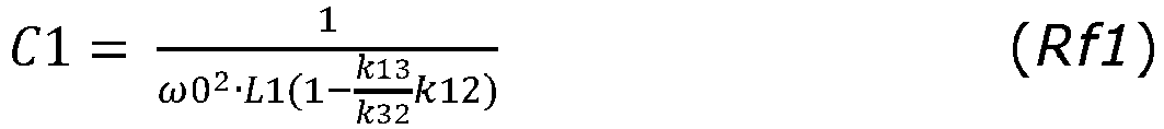


- In Eq. (Rf1), the calculation of the capacitance C1c of the
primary capacitor 114C is achieved by multiplying a value in a denominator by (1-k13 · k12 / k32) derived using a coupling coefficient, thus resulting in the value of the capacitance C1c greater than that derived using Eq. (1). In the non-power feeding mode in which thepower transmitter 100 delivers no electric power to thepower receiver 200, a target value of the capacitance of a capacitor required to decrease electrical current flowing through theprimary coil 112 to a selected value is constant. A range of change in capacitance C1c required to decrease the above electrical current to a given value in the non-power feeding mode may, therefore, be decreased to be smaller when the capacitance C1c is set to a small value using Eq. (1) than that when the capacitance C1c is set to a great value using Eq. (Rf1). For this reason, this embodiment uses Eq. (1) to determine the capacitance C1c, thereby enabling theprimary capacitor 114C working as a variable capacitor to be reduced in size. - The reason that after the detection signal Sd is delayed in time to change the capacitance C1c of the
primary capacitor 114C, the capacitance C3c of the tertiary capacitor 314C is changed is because the current flowing through theprimary coil 112 has been decreased at a time when the detection signal Sd is changed to the L-level, so that switching of the bidirectional switch SW1 of theprimary capacitor 114C at that time will result in a decreased risk that a high level of surge voltage may be generated by the switching of the bidirectional switch SW1, and the current flowing through thetertiary coil 312 usually decreases with a decrease in the capacitance C1c of theprimary capacitor 114C, so that the switching of the bidirectional switch SW3 of the tertiary capacitor 314C will also result in a decreased risk that a high level of surge voltage may be generated by the switching of the bidirectional switch SW1. In a case where the above generation of surge volage is permissible in the system, thedelay circuit 159 may be omitted. - The wireless power transmission system illustrated in
Fig. 11 includes the primaryresonant circuit 110D and the tertiaryresonant circuit 310D instead of the primaryresonant circuit 110C and the tertiaryresonant circuit 310C illustrated inFig. 10 and also includes the powerreceiver detecting circuit 150D instead of the powerreceiver detecting circuit 150C illustrated inFig. 10 . - The primary
resonant circuit 110D uses theprimary capacitor 114D that is a variable capacitor to variably change the capacitance C1d as a function of a control input in the form of the control voltage Vc. Similarly, the tertiaryresonant circuit 310D uses thetertiary capacitor 314D that is a typical variable capacitor to vary the capacitance C3d as a function of the control voltage Vc. - The power
receiver sensing circuit 150D is equipped with thevoltage conversion circuit 158D in connection with theprimary capacitor 114D and thetertiary capacitor 314D. Thevoltage conversion circuit 158D is used as thecomparator 158 of the powerreceiver sensing circuit 150C in the structure illustrated inFig. 10 . Thevoltage conversion circuit 158D is made of a differential amplifier circuit working to output the control voltage Vc as a function of a difference between the above-described detection voltage and the reference voltage Vrc. Thedelay circuit 159D is also provided which is used as thedelay circuit 159 in the structure ofFig. 10 . Thedelay circuit 159D works to delay the variable control voltage Vc in time. - The variable capacitors used as the
primary capacitor 114D and thetertiary capacitor 314D are designed to have capacitances decreasing with an elevation in level of the control voltage Vc. The control valve Vc outputted from thevoltage conversion circuit 158D needs to be controlled to be the voltage Vl in the power feeding mode which is developed in a condition where C1d = C1 and C3d = C3 and alternatively be the voltage Vh (>Vl) in the non-power feeding mode in a condition where C1d = Cs1 (<C1) and C3d = Cs3 (<C3). In order to meet such a need, thevoltage conversion circuit 158D is made of a differential amplifier circuit configured to have input of the detection voltage to an inverting input terminal (-) thereof and output the control voltage Vc which decreases with an elevation in level of the detection voltage derived by thecurrent measuring circuit 152. The variable capacitors (i.e., theprimary capacitor 114D and thetertiary capacitor 314D) may alternatively be designed to have characteristics inverse of those described above. In such a case, thevoltage conversion circuit 158D is designed to have the detection voltage inputted to a non-inverting input terminal (+) thereof. - The wireless power transmission system in
Fig. 11 , like that inFig. 10 , operates in the same way as in the first embodiment in the power feeding mode. The wireless power transmission system is also capable of reducing a loss of electric power arising from flow of a large amount of the standby current I1s in the non-power feeding mode. The control of operation of the alternating-current source 130 described in the fourth embodiment may be omitted. The risk that the leakage of magnetic flux may result from flow of the standby currents I1s and I3s may be eliminated. - The capacitance C1d of the
primary capacitor 114D in the power feeding mode may be determined, like the capacitance C1c of the primary capacitor 114c, to be relatively low. This reduces a range of change in the capacitance C1 in either of the power feeding mode and the non-power feeding mode, thereby facilitating use of a variable capacitor as theprimary capacitor 114D which has a capacitance variable as a function of the control input (i.e., the control valve Vc). - As apparent from the above discussion, the power
receiver sensing circuit 150D works as a capacitance controller to change the capacitances of theprimary capacitor 114D and thetertiary capacitor 314D. - In the structures of
Figs. 10 and11 , theprimary capacitors resonant circuits tertiary capacitors 314C and 314D of the tertiaryresonant circuits resonant circuits - The above-described fifth embodiment is a modification of the structure in the first embodiment (see
Fig. 1 ), but however, may alternatively designed to have a modified structure in the third embodiment (seeFig. 6 ). - The determination of circuit constants of each circuit installed in the wireless power transmission system is usually achieved based in a design condition where the
primary coil 112 and thesecondary coil 212 face each other (seeFigs. 1 and6 ), specifically, theprimary coil 112 and thesecondary coil 212 are oriented to have central axes thereof aligned with each other. In contrast, the determination of the capacitance of the secondary capacitor 214 to provide an enhanced power factor of ac power described in the first and third embodiments is preferably achieved in a design condition which will be described below in detail. - The following discussion on an example illustrated in
Fig. 12 assumes that thesecondary coil 212 moves closer to and then away from theprimary coil 112. A design condition may be considered in which the center axis CX2 of thesecondary coil 212 is located in one of regions Rd defined between a position -Ph and a coil end position -Pe and between a position +Ph and a coil end position +Pe in a direction in which thesecondary coil 212 moves. The coil ends -Pe and +Pe represent ends of theprimary coil 112 which are opposed to each other in the direction of movement of thesecondary coil 212. Each of the positions -Ph and +Ph is a position which is one-half of an interval between the center position Pc (i.e., position of the center axis CX1) of theprimary coil 112 and a corresponding one of the coil ends -Pe and +Pe away from a corresponding one of the coil ends -Pe and +Pe in the direction of movement of thesecondary coil 212. Such a design condition will also be referred to as a first design condition below. - Additionally, another design condition demonstrated in
Fig. 13 may be considered in which the center (i.e., the center axis) of thesecondary coil 212 is arranged on one of regions Rd between the center position Pc (i.e., position of the center axis CX1) of theprimary coil 112 and the position -Ph and between the center position Pc and the position +Ph in the direction in which thesecondary coil 212 moves. Each of the positions -Ph and +Ph is, as described above, a position which is one-half of an interval between the center position Pc of theprimary coil 112 and a corresponding one of the coil ends -Pe and +Pe away from the center position Pc in the direction of movement of thesecondary coil 212. Such a design condition will also be referred to as a second design condition below. -
Fig. 14 represents a comparison between power factors in a second setting example in the second design condition and in a first setting example in the first design condition. The first setting example is an example of the first design condition where an intermediate position between the coil end -Pe of theprimary coil 112 and the 1/2 position -Ph coincides with the center position of thesecondary coil 212. The second setting example is an example of the second design condition where the center position Pc of theprimary coil 112 coincides with the center position of thesecondary coil 212. - In the second setting example, the power factor decreases as the center position of the
secondary coil 212 moves away from a design point, that is, the center position Pc of theprimary coil 112. In contrast, in the first setting example, the power factor slightly drops near the center position Pc of theprimary coil 112, but is substantially kept constant over a wide range. It, therefore, follows that in order to ensure a high level of the power factor over an increased range in addition to a condition where the major surface of theprimary coil 112 faces that of thesecondary coil 212, the wireless power transmission system is preferably designed to satisfy the first design condition. - Although not illustrated, when a plurality of
primary coils 112 are arrayed in the direction of movement of the primary coils 112 (seeFigs. 12 and13 ), the wireless power transmission system is preferably configured to meet the second design condition, not the first design condition. If the wireless power transmission system is designed to meet the first design condition, electric powers transferred from the first coil and the second coil that are ones of theprimary coils 112, as demonstrated inFig. 15 , may overlap each other in a region around adjacent ends +Pe and -Pe of the first and second coils, thereby resulting in an increase in pulsation of the electric powers. In contrast, if the wireless power transmission system is designed to meet the second design condition, it, as can be seen inFig. 16 , results in a decreased overlap between electric powers delivered from the first and second coils located adjacent to each other, thus reducing the pulsation of the electric powers. - The wireless power transmission system in each of the above embodiments is equipped with a single pair of the primary resonant circuit and the tertiary resonant circuit, but however, may alternatively be designed to have a plurality of power transmitting units each of which includes a single pair of a primary resonant circuit and a tertiary resonant circuit in the way as described below.
- For instance, the wireless power transmission system may be designed to have a structure, as illustrated in
Fig. 17 , for use in automotive vehicles. The wireless power transmission system inFig. 17 is equipped with a plurality of power transmitting units each of which includes the primaryresonant circuit 110, the tertiaryresonant circuit 310, and the powerreceiver sensing circuit 150 illustrated inFig. 9 . The wireless power transmission system inFig. 17 is configured as a power feeding system which works to transfer electric power from thepower transmitter 100E disposed on or in a lane of the vehicle traffic road RS to the power receiver 200 (seeFig. 9 ) installed in the vehicle VH. The vehicle VH is implemented by an electric vehicle or a hybrid vehicle using electric power as traction power. InFig. 17 , the x-axis indicates a direction of forward movement of the vehicle VH along the lane of the vehicle traffic road RS. The y-axis indicates a width direction of the vehicle traffic road RS. The z-axis indicates a vertical direction. The same definition of the x-, y-, and z-axes applies to the following drawings. - The
power transmitter 100E is equipped with a plurality of power transmitting units each of which includes the primaryresonant circuit 110, the tertiaryresonant circuit 310, and the powerreceiver sensing circuit 150 illustrated inFig. 9 . Thepower transmitter 100E also includes the alternating-current source 130E. The alternating-current source 130E includes thepower circuit 132 and a plurality of powertransmission output circuits 134 which apply electric power to the primaryresonant circuits 110. - The primary coils 112 (see
Fig. 9 ) of the primaryresonant circuits 110 are arranged away from each other along the lane of the vehicle traffic road RS. Thetertiary coil 312 of each of the tertiaryresonant circuits 310 is stacked on a corresponding one of the primary coils 112 (seeFigs. 4 and5). - The
power circuit 132 works to convert ac power delivered from an external power supply into dc power. Each of the powertransmission output circuits 134 includes an inverter which converts the dc power supplied from thepower circuit 132 into ac power at the operating frequency. Each of the powertransmission output circuits 134 is controlled in operation by a corresponding one of the powerreceiver sensing circuits 150. - The
power receiver 200 mounted in the vehicle VH includes the secondaryresonant circuit 210, thepower receiving circuit 220, and the battery 230 (seeFig. 9 ). Thesecondary coil 212 of the secondaryresonant circuit 210 is arranged on the bottom of the vehicle VH, so that it may face theprimary coil 112 of one of the primary resonant circuits (seeFig. 4 ). The electric power induced in the secondaryresonant circuit 210 is used to charge thebatter 230 through thepower receiving circuit 220 for driving an electric motor, not shown. - Each of the power
receiver sensing circuits 150, as described in the fourth embodiment with reference toFig. 9 , works to detect the presence of thesecondary coil 212 to which it is required to transfer electric power from theprimary coil 112, in other words, the presence of the vehicle VH in which thepower receiver 200 is mounted. When detecting the presence of the vehicle VH, each of the powerreceiver sensing circuits 150 actuates a corresponding one of the powertransmission output circuits 134 to apply electric power to a corresponding one of the primaryresonant circuits 110 to transfer the electrical energy to thepower receiver 200 of the vehicle VH. When detecting the absence of the vehicle VH, each of the powerreceiver sensing circuits 150 deactivates a corresponding one of the powertransmission output circuits 134. - The wireless power transmission system in this embodiment offers substantially the same beneficial advantages as in the above embodiments.
- When there is no need to implement measures to deal with loss of electric power or leakage of magnetic flux, the power
receiver sensing circuits 150 may be omitted, and the powertransmission output circuits 134 may be kept on at all times. In a case where the input impedance Zin of the primaryresonant circuit 100 is, as described in the second embodiment, increased, thus resulting in an increase in drop in current flowing through the primaryresonant circuit 110 in the absence of thesecondary coil 212, the powerreceiver sensing circuits 150 may be omitted. In such a case, the wireless power transmission system may be designed to a single powertransmission output circuit 134. - The wireless power transmission system may be designed for the vehicle VH to have a structure illustrated in
Fig. 18 which is equipped with a plurality of power transmitting units each of which includes the primaryresonant circuit 110C, the tertiaryresonant circuit 310C, and the powerreceiver sensing circuit 150C illustrated inFig. 10 . The wireless power transmission system inFig. 18 is configured as a power feeding system which works to transfer electric power from thepower transmitter 100F disposed on or in the lane of the vehicle traffic road RS to the power receiver 200 (seeFig. 10 ) installed in the vehicle VH. - The
power transmitter 100F is equipped with a plurality of power transmitting units each of which includes the primaryresonant circuit 110C, the tertiaryresonant circuit 310C, and the powerreceiver sensing circuit 150C illustrated inFig. 10 . Thepower transmitter 100F is equipped with the alternating-current source 130F. The alternating-current source 130F is, unlike the alternating-current source 130E inFig. 17 , equipped with a single powertransmission output circuit 134. - The primary coils 112 (see
Fig. 10 ) of the primaryresonant circuits 110C are, like the primaryresonant circuits 110 inFig. 17 , arranged away from each other along the lane of the vehicle traffic road RS. Thetertiary coil 312 of each of the tertiaryresonant circuits 310C is, like the tertiaryresonant circuits 310 inFig. 17 , stacked on a corresponding one of the primary coils 112 (seeFigs. 4 and5). - The structure of the
power receiver 200 installed in the vehicle VH is the same as in the wireless power transmission system illustrated inFig. 17 . - Each of the power
receiver sensing circuits 150C, as described in the fifth embodiment with reference toFig. 10 , works to detect the presence of thesecondary coil 212 to which it is required to transfer electric power from theprimary coil 112, in other words, the presence of the vehicle VH in which thepower receiver 200 is mounted. When detecting the presence of the vehicle VH, each of the powerreceiver sensing circuits 150C changes the capacitance of theprimary capacitor 114C of a corresponding one of the primaryresonant circuits 110C to a capacitance used in the power feeding mode. The powertransmission output circuit 134 then applies electric power to the primaryresonant circuit 110C equipped with theprimary capacitor 114C whose capacitance has been changed to that used in the power feeding mode, thereby transferring electrical energy to thepower receiver 200 installed in the vehicle VH. When detecting the absence of the vehicle VH, each of the powerreceiver sensing circuits 150C changes the capacitance of theprimary capacitor 114C of a corresponding one of the primaryresonant circuits 110C to a capacitance used in the non-power feeding mode. This results in an increase in the input impedance Zin of the primaryresonant circuit 110C equipped with theprimary capacitor 114C whose capacitance has been changed to that used in the non-power feeding mode, thereby outputting no electric power to a corresponding one of the primaryresonant circuits 110C. In other words, the wireless power transmission system works to supply current only to the primaryresonant circuit 110C equipped with theprimary capacitor 114C regulated to have the capacitance set for use in the power feeding mode without supplying current to the primaryresonant circuits 110C equipped with theprimary capacitors 114C regulated to have the capacitances set for use in the non-power feeding mode. This minimizes a useless loss of electric power. As apparent from the above discussion, the wireless power transmission system in this embodiment is designed to use the single powertransmission output circuit 134 to operate the plurality of primaryresonant circuits 110C. - The wireless power transmission system in this embodiment offers substantially the same beneficial advantages as in the above embodiments.
- Although not illustrated and described in detail, the wireless power transmission system for vehicles may be designed to include a plurality of primary
resonant circuits 110D, a plurality of tertiaryresonant circuits 310D, and a plurality of powerreceiver sensing circuits 150D. - The above-described wireless power transmission systems for vehicles illustrated in
Figs. 17 and18 are designed to use the structure in the first embodiment (seeFig. 1 ), but however, may alternatively be constructed to use the structure in the third embodiment (seeFig. 6 ). - The above-described the wireless power transmission system designed for vehicles which includes the power transmitting units each of which the primary resonant circuit and the tertiary resonant circuit offers substantially the same beneficial advantages as those in the above embodiments.
- This disclosure is not limited to the above embodiments, but may be realized by various embodiments without departing from the purpose of the disclosure. For instance, technical features described in the embodiments which correspond to those referred to in the summary of the invention may be replaced with each other or combined in different ways in order to solve at least a portion of the problems or ensure at least a portion of the beneficial effects. The technical features may be omitted unless otherwise they are stated as being essential in in principle.
Claims (13)
- A wireless power transmission system which works to supply electric power wirelessly from a power transmitter to a power receiver, comprising:a power transmitter (100, 100E, 100F) which includes a primary resonant circuit (110, 110B, 110C, 110D) and an alternating-current source (130, 130E, 130F), the primary resonant circuit including a primary coil (112) and a primary capacitor (114, 114C, 114D) for use in power transmission, the alternating-current source (130, 130E, 130F) working to apply ac power at a given operating frequency to the primary resonant circuit;a power receiver (200) which includes a secondary resonant circuit (210), the secondary resonant circuit including a secondary coil (212) and a secondary capacitor (214) for use in a power reception, the secondary coil being to be magnetically coupled with the primary coil; anda tertiary resonant circuit (310, 310B, 310C, 310D) which includes a tertiary coil (312) and a tertiary capacitor (314, 314C, 314D), the tertiary coil being arranged to achieve magnetic coupling with the primary coil and the secondary coil, the tertiary capacitor constituting a short-circuit resonant circuit along with the tertiary coil,the primary coil has a self-inductance L1, a capacitance of the primary capacitor is set to a capacitance C1, as given by Eq. (1) below, to cause resonance in the primary capacitor and the primary coil at an angular frequency ω0 that is the operating frequency,
 the tertiary coil has a self-inductance L3, a capacitance of the tertiary capacitor is set to a capacitance C3, as given by Eq. (2) below, to cause resonance in the tertiary capacitor and the tertiary coil at the operating frequency,
 a capacitance of the secondary capacitor is determined to decrease a reactive component of the ac power which arises from the self-inductances and mutual inductances of the primary coil, the secondary coil, and the tertiary coil.
 - The wireless power transmission system as set forth in claim 1, wherein the capacitance of the secondary capacitor is set to a value greater than a capacitance C2r given by Eq. (3) below expressed by the self-inductance L2 of the secondary coil and the angular frequency ω0,

- The wireless power transmission system as set forth in claim 2, wherein the capacitance of the secondary capacitor is set to a capacitance C2 given by Eq. (4) below expressed by a self-inductance L2 of the secondary coil, a mutual inductance M12 of the primary coil and the secondary coil, a mutual inductance M13 of the primary coil and the tertiary coil, a mutual inductance M32 of the tertiary coil and the secondary coil, and the angular frequency ω0,

- The wireless power transmission system as set forth in claim 2, wherein the capacitance of the secondary capacitor is set in a range of a value of the capacitance C2 and the value of the capacitance C2 +25%, the value of the capacitance C2 being given by Eq. (4) below expressed by a self-inductance L2 of the secondary coil, a mutual inductance M12 of the primary coil and the secondary coil, a mutual inductance M13 of the primary coil and the tertiary coil, a mutual inductance M32 of the tertiary coil and the secondary coil, and the angular frequency ω0,
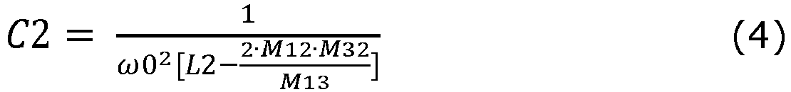
- The wireless power transmission system as set forth in claim 2, wherein the tertiary coil connects in series with the primary coil, the tertiary capacitor connects in parallel to the tertiary coil, the capacitance of the secondary capacitor is set to a capacitance C2 given by Eq. (5) below expressed by a self-inductance L2 of the secondary coil, a self-inductance L3 of the tertiary coil, a mutual inductance M12 of the primary coil and the secondary coil, a mutual inductance M13 of the primary coil and the tertiary coil, a mutual inductance M32 of the tertiary coil and the secondary coil, and the angular frequency ω0,

- The wireless power transmission system as set forth in claim 2, wherein the tertiary coil connects in series with the primary coil, the tertiary capacitor connects in parallel to the tertiary coil, the capacitance of the secondary capacitor is set in a range of a value of the capacitance C2 and the value of the capacitance C2 +25%, the value of the capacitance C2 being given by Eq. (5) below expressed by a self-inductance L2 of the secondary coil, a self-inductance L3 of the tertiary coil, a mutual inductance M12 of the primary coil and the secondary coil, a mutual inductance M13 of the primary coil and the tertiary coil, a mutual inductance M32 of the tertiary coil and the secondary coil, and the angular frequency ω0,

- The wireless power transmission system as set forth in any one of claims 1 to 6, wherein the tertiary coil is arranged in a constant state of coupling with the primary coil.
- The wireless power transmission system as set forth in claim 7, wherein the primary coil and the tertiary coil are formed integrally in a form of a printed circuit board, and the secondary capacitor and the tertiary capacitor are mounted on the printed circuit board.
- The wireless power transmission system as set forth in claim 7 or 8, wherein the primary capacitor (114C, 114D) is made of a variable capacitor whose capacitance is variable, and further comprising a capacitance controller (150C, 150D) which works to measure a coil current flowing through the primary coil and changes the capacitance of the primary capacitor as a function of a value of the coil current, the capacitance controller working to set the capacitance of the primary capacitor to a value lower than the value of the capacitance C1 given by Eq. (1) above when the value of the coil current decreases.
- The wireless power transmission system as set forth in claim 9, wherein the tertiary capacitor is made of a variable capacitor whose capacitance is variable, and the capacitance controller works to decrease a capacitance of the tertiary capacitor to a value lower than the capacitance C3 given by Eq. (2) above.
- The wireless power transmission system as set forth in claim 10, wherein the capacitance controller decreases the capacitance of the primary capacitor and then decreases the capacitance of the tertiary capacitor.
- The wireless power transmission system as set forth in any one of claims 7 to 11, wherein the secondary coil moves closer to or away from the primary coil, and the capacitance of the secondary capacitor is determined based on a state of coupling between the primary coil and the secondary coil, a state of coupling between the primary coil and the tertiary coil, and a state of coupling between the tertiary coil and the secondary coil in a condition where a center of the secondary coil lies in one of regions between a first coil end of the primary coil and a position which is one-half of an interval between the center of the primary coil and the first coil end away from the first coil end and between a second coil end of the primary coil and a position which is one-half of the interval away from the second coil end in a direction in which the secondary coil moves closer to or away from the primary coil.
- The wireless power transmission system as set forth in any one of claims 7 to 11, wherein the secondary coil moves closer to or away from the primary coil, and the capacitance of the secondary capacitor is determined based on a state of coupling between the primary coil and the secondary coil, a state of coupling between the primary coil and the tertiary coil, and a state of coupling between the tertiary coil and the secondary coil in a condition where a center of the secondary coil lies in one of regions between a center of the primary coil and a position which is one-half of an interval between the center of the primary coil and the first coil end away from the center of the primary coil and between the center of the primary coil and a position which is one-half of the interval away from the center of the primary coil in a direction in which the secondary coil moves closer to or away from the primary coil.
Applications Claiming Priority (3)
| Application Number | Priority Date | Filing Date | Title |
|---|---|---|---|
| JP2021028217 | 2021-02-25 | ||
| JP2022008670A JP2022130305A (en) | 2021-02-25 | 2022-01-24 | Contactless power supply system |
| PCT/JP2022/004229 WO2022181280A1 (en) | 2021-02-25 | 2022-02-03 | Contactless power feeding system |
Publications (1)
| Publication Number | Publication Date |
|---|---|
| EP4300522A1 true EP4300522A1 (en) | 2024-01-03 |
Family
ID=83048216
Family Applications (1)
| Application Number | Title | Priority Date | Filing Date |
|---|---|---|---|
| EP22759320.9A Pending EP4300522A1 (en) | 2021-02-25 | 2022-02-03 | Contactless power feeding system |
Country Status (3)
| Country | Link |
|---|---|
| US (1) | US20230387723A1 (en) |
| EP (1) | EP4300522A1 (en) |
| WO (1) | WO2022181280A1 (en) |
Family Cites Families (3)
| Publication number | Priority date | Publication date | Assignee | Title |
|---|---|---|---|---|
| US6317338B1 (en) | 1997-05-06 | 2001-11-13 | Auckland Uniservices Limited | Power supply for an electroluminescent display |
| JP6323312B2 (en) * | 2014-11-26 | 2018-05-16 | パナソニックIpマネジメント株式会社 | Contactless power supply system |
| JP6696563B2 (en) * | 2016-03-18 | 2020-05-20 | 株式会社村田製作所 | Power transmitting device, power receiving device, and wireless power feeding system |
-
2022
- 2022-02-03 EP EP22759320.9A patent/EP4300522A1/en active Pending
- 2022-02-03 WO PCT/JP2022/004229 patent/WO2022181280A1/en active Application Filing
-
2023
- 2023-08-10 US US18/232,690 patent/US20230387723A1/en active Pending
Also Published As
| Publication number | Publication date |
|---|---|
| US20230387723A1 (en) | 2023-11-30 |
| WO2022181280A1 (en) | 2022-09-01 |
Similar Documents
| Publication | Publication Date | Title |
|---|---|---|
| EP2320538B1 (en) | Resonance type non-contact charging apparatus | |
| EP3654490B1 (en) | Contactless power transmission system | |
| US9601946B2 (en) | Wireless power transmitter, wireless power receiver and wireless power transmission method | |
| US10756576B2 (en) | Feed unit, electronic, unit, and feed system | |
| US9601271B2 (en) | Detecting device, power supply system, and detecting device control method | |
| WO2012014482A1 (en) | Resonance type non-contact power supply system | |
| US9793747B2 (en) | Wireless power receiving device and power control method thereof | |
| US20130082648A1 (en) | Power receiving device and contactless power feeding system | |
| KR101478930B1 (en) | Contactless power feeding apparatus | |
| EP2357717A1 (en) | Non-contact power transmission apparatus and power transmission method using a non-contact power transmission apparatus | |
| US20120169136A1 (en) | Non-resonant and quasi-resonant system for wireless power transmission to multiple receivers | |
| EP3282539A1 (en) | Power transmission device, vehicle equipped with power transmission device, and wireless power transmission system | |
| US20140300196A1 (en) | Feed unit and feed system | |
| US20120223591A1 (en) | Overvoltage protection circuit, power transmission device including the same, and control method thereof | |
| KR20050013605A (en) | Planar resonator for wireless power transfer | |
| JP2013027129A (en) | Power feeding side facility and resonance type non-contact power feeding system | |
| US20190393728A1 (en) | Multi-Mode Wireless Power Receiver Control | |
| CN104541435A (en) | Power transmission system | |
| CN104521101A (en) | Power transmission system | |
| CN109103996A (en) | Wireless power transmission system, power transmission device and power receiving device | |
| EP4300522A1 (en) | Contactless power feeding system | |
| KR101765051B1 (en) | Overvoltage protection circuit, power transfer apparatus comprising it and control method of power transfer apparatus | |
| CN110336389B (en) | Wireless power receiving device and wireless power transmission system | |
| JP2018170838A (en) | Power receiver, power transmission system, and control method for power receiver | |
| US20190299800A1 (en) | Wireless power transmission device and wireless power transmission system |
Legal Events
| Date | Code | Title | Description |
|---|---|---|---|
| STAA | Information on the status of an ep patent application or granted ep patent |
Free format text: STATUS: THE INTERNATIONAL PUBLICATION HAS BEEN MADE |
|
| PUAI | Public reference made under article 153(3) epc to a published international application that has entered the european phase |
Free format text: ORIGINAL CODE: 0009012 |
|
| STAA | Information on the status of an ep patent application or granted ep patent |
Free format text: STATUS: REQUEST FOR EXAMINATION WAS MADE |
|
| 17P | Request for examination filed |
Effective date: 20230809 |
|
| AK | Designated contracting states |
Kind code of ref document: A1 Designated state(s): AL AT BE BG CH CY CZ DE DK EE ES FI FR GB GR HR HU IE IS IT LI LT LU LV MC MK MT NL NO PL PT RO RS SE SI SK SM TR |