EP4300319A1 - Hot plugging method and apparatus for memory module, and memory module - Google Patents
Hot plugging method and apparatus for memory module, and memory module Download PDFInfo
- Publication number
- EP4300319A1 EP4300319A1 EP22760642.3A EP22760642A EP4300319A1 EP 4300319 A1 EP4300319 A1 EP 4300319A1 EP 22760642 A EP22760642 A EP 22760642A EP 4300319 A1 EP4300319 A1 EP 4300319A1
- Authority
- EP
- European Patent Office
- Prior art keywords
- memory
- power
- abnormal
- key
- output interface
- Prior art date
- Legal status (The legal status is an assumption and is not a legal conclusion. Google has not performed a legal analysis and makes no representation as to the accuracy of the status listed.)
- Withdrawn
Links
Images



Classifications
-
- G—PHYSICS
- G06—COMPUTING OR CALCULATING; COUNTING
- G06F—ELECTRIC DIGITAL DATA PROCESSING
- G06F3/00—Input arrangements for transferring data to be processed into a form capable of being handled by the computer; Output arrangements for transferring data from processing unit to output unit, e.g. interface arrangements
- G06F3/06—Digital input from, or digital output to, record carriers, e.g. RAID, emulated record carriers or networked record carriers
- G06F3/0601—Interfaces specially adapted for storage systems
- G06F3/0602—Interfaces specially adapted for storage systems specifically adapted to achieve a particular effect
- G06F3/0614—Improving the reliability of storage systems
- G06F3/0619—Improving the reliability of storage systems in relation to data integrity, e.g. data losses, bit errors
-
- G—PHYSICS
- G06—COMPUTING OR CALCULATING; COUNTING
- G06F—ELECTRIC DIGITAL DATA PROCESSING
- G06F13/00—Interconnection of, or transfer of information or other signals between, memories, input/output devices or central processing units
- G06F13/38—Information transfer, e.g. on bus
- G06F13/40—Bus structure
- G06F13/4063—Device-to-bus coupling
- G06F13/4068—Electrical coupling
- G06F13/4081—Live connection to bus, e.g. hot-plugging
-
- G—PHYSICS
- G06—COMPUTING OR CALCULATING; COUNTING
- G06F—ELECTRIC DIGITAL DATA PROCESSING
- G06F1/00—Details not covered by groups G06F3/00 - G06F13/00 and G06F21/00
- G06F1/16—Constructional details or arrangements
- G06F1/18—Packaging or power distribution
- G06F1/183—Internal mounting support structures, e.g. for supporting printed circuit boards
- G06F1/185—Mounting of expansion boards
- G06F1/186—Securing of expansion boards in correspondence to slots provided at the computer enclosure
-
- G—PHYSICS
- G06—COMPUTING OR CALCULATING; COUNTING
- G06F—ELECTRIC DIGITAL DATA PROCESSING
- G06F1/00—Details not covered by groups G06F3/00 - G06F13/00 and G06F21/00
- G06F1/26—Power supply means, e.g. regulation thereof
- G06F1/266—Arrangements to supply power to external peripherals either directly from the computer or under computer control, e.g. supply of power through the communication port, computer controlled power-strips
-
- G—PHYSICS
- G06—COMPUTING OR CALCULATING; COUNTING
- G06F—ELECTRIC DIGITAL DATA PROCESSING
- G06F11/00—Error detection; Error correction; Monitoring
- G06F11/07—Responding to the occurrence of a fault, e.g. fault tolerance
- G06F11/14—Error detection or correction of the data by redundancy in operations
- G06F11/1402—Saving, restoring, recovering or retrying
- G06F11/1415—Saving, restoring, recovering or retrying at system level
- G06F11/1441—Resetting or repowering
-
- G—PHYSICS
- G06—COMPUTING OR CALCULATING; COUNTING
- G06F—ELECTRIC DIGITAL DATA PROCESSING
- G06F11/00—Error detection; Error correction; Monitoring
- G06F11/07—Responding to the occurrence of a fault, e.g. fault tolerance
- G06F11/16—Error detection or correction of the data by redundancy in hardware
- G06F11/1658—Data re-synchronization of a redundant component, or initial sync of replacement, additional or spare unit
-
- G—PHYSICS
- G06—COMPUTING OR CALCULATING; COUNTING
- G06F—ELECTRIC DIGITAL DATA PROCESSING
- G06F3/00—Input arrangements for transferring data to be processed into a form capable of being handled by the computer; Output arrangements for transferring data from processing unit to output unit, e.g. interface arrangements
- G06F3/06—Digital input from, or digital output to, record carriers, e.g. RAID, emulated record carriers or networked record carriers
- G06F3/0601—Interfaces specially adapted for storage systems
- G06F3/0628—Interfaces specially adapted for storage systems making use of a particular technique
- G06F3/0646—Horizontal data movement in storage systems, i.e. moving data in between storage devices or systems
- G06F3/0647—Migration mechanisms
-
- G—PHYSICS
- G06—COMPUTING OR CALCULATING; COUNTING
- G06F—ELECTRIC DIGITAL DATA PROCESSING
- G06F3/00—Input arrangements for transferring data to be processed into a form capable of being handled by the computer; Output arrangements for transferring data from processing unit to output unit, e.g. interface arrangements
- G06F3/06—Digital input from, or digital output to, record carriers, e.g. RAID, emulated record carriers or networked record carriers
- G06F3/0601—Interfaces specially adapted for storage systems
- G06F3/0628—Interfaces specially adapted for storage systems making use of a particular technique
- G06F3/0646—Horizontal data movement in storage systems, i.e. moving data in between storage devices or systems
- G06F3/065—Replication mechanisms
-
- G—PHYSICS
- G06—COMPUTING OR CALCULATING; COUNTING
- G06F—ELECTRIC DIGITAL DATA PROCESSING
- G06F3/00—Input arrangements for transferring data to be processed into a form capable of being handled by the computer; Output arrangements for transferring data from processing unit to output unit, e.g. interface arrangements
- G06F3/06—Digital input from, or digital output to, record carriers, e.g. RAID, emulated record carriers or networked record carriers
- G06F3/0601—Interfaces specially adapted for storage systems
- G06F3/0668—Interfaces specially adapted for storage systems adopting a particular infrastructure
- G06F3/0671—In-line storage system
- G06F3/0673—Single storage device
Definitions
- the disclosure relates to the technical field of integrated circuits, and particularly, to a method for hot swapping a memory, a device for hot swapping a memory, and a memory.
- Dual-inline-memory-modules provide 64-bit data channels and are widely used.
- a method for hot swapping a memory which includes that: in response to a triggering operation of a replacement key of an abnormal memory, data on an abnormal memory is copied to an idle memory when a system is in a powered on state; the abnormal memory is powered off and replaced with a new memory after the data is copied; and in response to a triggering operation of a power on key of the new memory, the new memory is powered on.
- the operation that the abnormal memory is powered off includes that: a power management IC enable signal corresponding to the abnormal memory is pulled down, to power off the abnormal memory.
- the method further includes that: the abnormal memory is removed from a memory mapping table of the system.
- the method further includes that: the new memory is added into the memory mapping table of the system.
- the method further includes that: a physical address of the abnormal memory is determined according to a logical address of abnormal data.
- the operation that the data on the abnormal memory is copied to the idle memory includes that: a writing operation on the abnormal memory is stopped, and the data in the abnormal memory is stored into a cache through a reading operation; and the data in the cache is written into the idle memory.
- the operation that the new memory is powered on includes that: a power management IC enable signal corresponding to the new memory is pulled up to power on the new memory.
- a device for hot swapping a memory which includes: a data copying module configured to, , in response to a triggering operation of a replacement key of an abnormal memory, copy data on the abnormal memory to an idle memory when a system is powered on; a power off module configured to power off the abnormal memory and replace the abnormal memory with a new memory after the data is copied; and a power on module configured to, in response to a triggering operation of a power on key of the new memory, power on the new memory.
- a memory which includes: a memory body, and a replacement key and a power on key arranged on the memory body.
- the replacement key and the power on key are separately connected to a hub through an input/output interface.
- the hub is configured to send a system management bus signal to a central processing unit (CPU) when level conversion occurs at the input/output interface.
- the CPU is configured to power on or power off the memory after receiving the system management bus signal.
- the memory further includes a first power supply and a first resistor.
- the input/output interface is grounded through the replacement key.
- the first power supply is arranged on a connecting line between the input/output interface and the replacement key.
- the first resistor is arranged on a connecting line of the first power supply.
- the memory further includes a second power supply and a second resistor.
- the input/output interface is grounded through the power on key.
- the second power supply is arranged on the connecting line between the input/output interface and the power on key.
- the second resistor is arranged on a connecting line of the second power supply.
- the memory further includes a third power supply.
- the input/output interface is grounded.
- the replacement key is arranged between the third power supply and the input/output interface.
- the memory further includes a fourth power supply.
- the input/output interface is grounded.
- the power on key is arranged between the fourth power supply and the input/output interface.
- both the power on key and the replacement key are switches.
- the CPU is connected to a power management IC of the memory.
- the CPU controls the memory to be powered off by pulling down a power management IC enable signal; and the CPU controls the memory to be powered on by pulling up the power management IC enable signal.
- DDR4 is the abbreviation of the fourth generation DDR SDRAM
- DDR5 is the abbreviation of the fifth generation DDR SDRAM
- DDR SDRAM is the abbreviation of Double Data Rate SDRAM in English
- SDRAM is the abbreviation of Synchronous Dynamic Random Access Memory.
- the synchronization object is a system clock frequency. Therefore, in combination, DDR4 is the fourth generation double rate synchronous dynamic random access memory, and DDR5 is the fifth generation double rate synchronous dynamic random access memory. From DDR4 to DDR5, a power supply unit of a DIMM memory has been moved from a mainboard to the DIMM memory. The power supply on each DIMM memory is independent. Therefore, each DIMM memory may be powered on and powered off independently.
- the embodiments of the disclosure provide a method for hot swapping a memory, which is applied to a memory that can supply power to a memory module, such as DDR5, independently, thus can replace an abnormal memory without shutting down a system, so as to realize a hot-swap mode of the memory.
- the method for hot swapping a memory may include the following operations.
- the abnormal memory is powered off and replaced with a new memory after the data is copied.
- the new memory is powered on.
- the data on the abnormal memory may be copied to an idle memory first in response to the triggering operation of the replacement key of the abnormal memory when the system is in a working state, and only the abnormal memory is powered off after the data is copied; then, the abnormal memory may be replaced with a new memory; and the new memory may be powered on in response to the triggering operation of the power on key of the new memory.
- the whole process described above may realize an abnormal memory replacement process when the system is in the working state, that is, a method for hot swapping a memory.
- the data on the abnormal memory is copied to the idle memory in response to the triggering operation of the replacement key of the abnormal memory when the system is powered on.
- the system may include a computer system or a server system, which is a machine system that receives and stores information according to human requirements, automatically performs data processing and calculation, and outputs result information.
- the system usually needs to store data. Therefore, the system also includes a memory. During working, data may be read from the memory or may be stored in the memory.
- the system in a powered on state may be that the system is in a startup state, or the system is in a working state, for example, a state that the system is performing a data access operation and the like.
- the system in the powered on state may be understood that the system is not in a shutdown state, and the system does not need to be shut down during the whole swapping process of the memory.
- the abnormal memory may be a memory with a data reading error, that is, abnormal data are found in the abnormal memory.
- a physical address of the abnormal memory is determined according to the logical address of abnormal data after the abnormal data is found.
- FIG. 2 illustrates a flowchart of determining an abnormal memory from abnormal data.
- the MC may acquire the logical address of the abnormal data from a logical address mapping area, and the MC then coverts the logical address of the abnormal data into a physical address of the abnormal memory according to a conversion relationship between the logical address and the physical address, so that a corresponding DIMM memory may be found according to the physical address.
- a physical address mapping area in the MC corresponds to a memory physical address in a memory mapping table. A specific abnormal memory may be determined from the physical address in the physical address mapping area.
- the replacement key may be a physical key arranged on the abnormal memory or a virtual key added on a baseboard management controller (BMC) interface.
- BMC baseboard management controller
- the replacement key is connected to the CPU of the system through a hub, and thus informs the CPU or the MC through a system management bus (Smbus) or an improved inter integrated circuit (13C) signal, that the corresponding memory needs to be powered off and replaced.
- Smbus system management bus
- 13C improved inter integrated circuit
- the data in the abnormal memory may be copied to an idle memory in response to a triggering operation of the replacement key, so as to save the data in the abnormal memory.
- the triggering operation of the replacement key may be a single-click operation, a double-click operation, a long press operation, or other triggering operations. There are no special limits made to specific forms of the triggering operations in the exemplary implementation mode of the disclosure.
- FIG. 3 illustrates a flowchart of copying data of the abnormal memory.
- a writing operation on the abnormal memory needs to be stopped first, and new data is not written into the abnormal memory any longer, so as to prevent data loss.
- the data in the abnormal memory may be read through a reading operation, and the read data may be stored in a cache that can temporarily store the data.
- the data in the cache may be written into an idle memory other than the abnormal memory.
- the idle memory here may be a normal memory that stores some data or a normal memory that does not store any data.
- the abovementioned data copying process of the abnormal memory may be executed by an MC.
- the abnormal memory is powered off after the data is copied, and the abnormal memory is replaced with a new memory.
- the abnormal memory is powered off.
- a specific powering off operation may be that the abnormal memory is powered off by pulling down a power management IC enable signal corresponding to the abnormal memory after the CPU or the MC receives the Smbus or the I3C signal.
- the power management IC enable signal is an enable signal when the power management IC (PMIC) works.
- whether the abnormal memory has been powered off may also be indicated by an indicating lamp.
- the replacement key is set as a key with a double-color indicating lamp. After the replacement key is pressed down, the color of the indicating lamp changes, which indicates that abnormal memory has been powered off.
- the abnormal memory After the abnormal memory is powered off, the abnormal memory may be replaced with a new memory. This process may be operated manually.
- the record of the abnormal memory further needs to be removed from the memory mapping table of the system, so that the system does not record the abnormal memory any longer.
- the memory mapping table is a record table that stores the physical addresses of memories.
- the abnormal memory record usually needs to be removed from the memory mapping table, so that the system can acquire the physical address of a normal memory from the memory mapping table.
- the new memory is powered on in response to the triggering operation of the power on key of the new memory.
- a newly inserted memory needs a triggering operation after the abnormal memory is replaced with the new memory.
- the triggering operation may be a single-click operation, a double-click operation, a long press operation, or other triggering operations. There are no special limits made to specific forms of the triggering operation in the exemplary embodiment of the disclosure.
- the power on key may inform the CPU or the MC to perform power-on initialization of the new memory.
- the power on key may be a physical key arranged on the new memory or a virtual key added on the BMC interface.
- the power on key is connected to the CPU or the MC of the system through a hub, and informs the CPU or the MC by a Smbus or an I3C signal that the corresponding memory needs to power on.
- a specific powering on operation may be that the new memory is powered on by pulling up a power management IC enable signal corresponding to the new memory after the CPU or the MC receives the Smbus or the I3C signal.
- the power management IC enable signal is an enable signal when a Power Management IC (PMIC) works.
- whether a new memory has been powered on may also be indicated by an indicating lamp.
- the power on key is set as a key with a double-color indicating lamp. After the power on key is pressed down, the color of the indicating lamp changes, so as to indicate that the new memory has been powered off.
- the system also needs to initialize and adjust the new memory to have an optimal state. After that, the system may record the new memory to the memory mapping table of the system for normal use of the system.
- the initialization and adjustment of the new memory belong to conventional technical means, which will not be elaborated herein.
- an abnormal memory may be powered off and replaced with a new memory after the data on the abnormal memory is copied to an idle memory in response to a triggering operation of a replacement key of the abnormal memory when the system is in a powered on state. That is, it is unnecessary to shut down the system in the replacement process of the abnormal memory, and there is no time spent for shutting down the system in the replacement process, so that the time consumption for replacing the abnormal memory can be reduced. It is convenience for a user with implementation of the hot swap mode for an abnormal memory when the system is powered on or in a working state.
- FIG. 4 illustrates a flowchart of operations of the method for hot swapping the memory provided by an exemplary implementation mode of the disclosure.
- S401 is entered.
- a replacement key of an abnormal memory is triggered.
- S402 data on the abnormal memory is copied to an idle memory in response to the triggering operation of the replacement key of the abnormal memory, referred to as data copying for short.
- S403, a power management IC enable signal is pulled down to power off the abnormal memory after the data is copied.
- the abnormal memory is replaced with a new memory after the abnormal memory is powered off.
- S405 a power on key of the new memory is triggered.
- S406 the new memory is powered on and initialized in response to the triggering operation of the power on key of the new memory.
- S407 after initialization, the new memory is added to the memory mapping table of the system, so that the new memory can work normally.
- the exemplary implementation mode of the disclosure further provides a device for hot swapping a memory.
- the hot swapping device 500 of a memory includes: a data copying module 510, a power off module 520, a power on module 530, a removal module 540, an addition module 550, and an address determination module 560.
- the data copying module 510 may be configured to, in response to a triggering operation of a replacement key of the abnormal memory, copy data on an abnormal memory to an idle memory, when a system is powered on.
- the power off module 520 may be configured to power off the abnormal memory and replace the abnormal memory with a new memory after the data is copied.
- the power on module 530 may be configured to, in response to a triggering operation of a power on key of the new memory, power on the new memory.
- the power off module 520 may be configured to pull down a power management IC enable signal corresponding to the abnormal memory to power off the abnormal memory.
- the removal module 540 may be configured to remove the abnormal memory from a memory mapping table of the system.
- the addition module 550 may be configured to add the new memory to the memory mapping table of the system.
- the address determination module 560 may be configured to determine a physical address of the abnormal memory according to a logical address of abnormal data.
- the data copying module 510 may be configured to stop a writing operation on the abnormal memory, store the data in the abnormal memory in a cache through a reading operation, and write the data in the cache into the idle memory.
- the power on module 530 may be configured to pull up a power management IC enable signal corresponding to the new memory to power on the new memory.
- an exemplary implementation mode of the disclosure further provides a memory capable of applying the method for hot swapping a memory.
- the memory includes: a memory body 610, a replacement key 620 and a power on key 630 arranged on the memory body 610.
- the replacement key 620 and the power on key 630 are separately connected to a hub HUB640 through an input/output interface IO.
- the hub 640 may be configured to send a system management bus signal to a CPU when level conversion occurs at the input/output interface IO. That is to say, the hub 640 needs to be connected with the CPU.
- the CPU may be an element independent from the memory in the system.
- the memory needs to be connected to the CPU through the hub 640, so as to power on or power off the memory through the CPU. That is, the CPU can power on or power off the memory after receiving the system management bus signal.
- the input/output interface IO connected to the replacement key 620 and the power on key 630 may be different pins of the same IO IC.
- One pin is connected to the replacement key 620 and the other pin is connected to the power on key 630.
- the system management bus signal may include the Smbus or I3C signal described in the foregoing embodiments.
- the level conversion of the input/output interface IO may be that the level at the input/output interface IO is converted from a high level to a low level when the replacement key 620 is triggered; or the level at the input/output interface IO is converted from a low level to a high level when the replacement key 620 is triggered.
- the level conversion of the input/output interface IO may also be that the level at the input/output interface IO is converted from a high level to a low level when the power on key 630 is triggered; or the level at the input/output interface IO is converted from a low level to a high level when the power on key 630 is triggered.
- the memory may further include a first power supply 710 and a first resistor 720.
- the input/output interface IO is grounded through the replacement key 620, and the first power supply 710 is arranged on a connecting line between the input/output interface IO and the replacement key 620 to provide a high level for the input/output interface IO.
- the first resistor 720 is also arranged on the connecting line of the first power supply 710, and the first resistor 720 can achieve an effect of stabilizing the voltage.
- the resistance of the first resistor 720 may be set according to actual situations. There are no special limits made thereto in the exemplary implementation mode of the disclosure.
- the input/output interface IO is communicated with a ground terminal, so that the level at the input/output interface IO will be converted from a high level to a low level.
- the input/output interface IO here may be a first pin 1 of an IO chip.
- the replacement key 620 may be a switch, and the input/output interface IO and the ground terminal may be conducted when the replacement key 620 is pressed down.
- the memory may further include a second power supply 730 and a second resistor 740.
- the input/output interface IO is grounded through the power on key 630, and the second power supply 730 is arranged on a connecting line between the input/output interface IO and the power on key 630 to provide a high level for the input/output interface IO.
- the second resistor 740 is also arranged on the connecting line of the second power supply 730, and the second resistor 740 can achieve an effect of stabilizing the voltage.
- the resistance of the second resistor 740 may be set according to actual situations. There are no special limits made thereto in the exemplary implementation mode of the disclosure.
- the input/output interface IO is communicated with a ground terminal, so that the level at the input/output interface IO will be converted from a high level to a low level.
- the input/output interface IO here may be a second pin 2 of an IO chip.
- the power on key 630 may be a switch, and the input/output interface IO and the ground terminal may be conducted when the power on key 630 is pressed down.
- the memory may further include a third power supply 810.
- the input/output interface IO is directly grounded to provide a low level for the input/output interface IO.
- the replacement key 620 is arranged between the third power supply 810 and the input/output interface IO. When the replacement key 620 is pressed down or triggered, the third power supply 810 will be conducted with the input/output interface IO, so that the level at the input/output interface IO is converted from a low level to a high level.
- the input/output interface IO here may be a first pin 1 of an IO chip.
- a resistor may or may not be arranged beside the third power supply 810. There are no special limits made thereto in the exemplary implementation mode of the disclosure. The resistance of the resistor may also be set according to actual situations. There are no limits made thereto herein.
- the replacement key 620 may be a switch, and the third power supply 810 and the input/output interface IO may be conducted when the replacement key 620 is pressed down.
- the memory may further include a fourth power supply 820.
- the level at the input/output interface IO is a low level at first.
- the power on key 630 is arranged between the fourth power supply 820 and the input/output interface IO.
- the fourth power supply 820 will be conducted with the input/output interface IO, so that the level at the input/output interface IO is converted from a low level to a high level.
- the input/output interface IO here may be a second pin 2 of an IO chip.
- the abovementioned power on key 630 may be a switch, and the fourth power supply 820 and the input/output interface IO may be conducted when the power on key 630 is pressed down.
- the CPU in order to power on or off the memory through the CPU, as shown in FIG. 6 , the CPU also needs to be connected to the power management IC PMIC650 of the memory.
- the CPU can control the memory to be powered off by pulling down the power management IC enable signal; and the CPU can control the memory to be powered on by pulling up the power management IC enable signal.
- the input/output interface IO is connected to a connecting finger of the memory through a hub.
- the hub is connected to the CPU by the connecting finger through the wiring on the mainboard, so as to realize the transmission of signals.
- the memory provided by the embodiments of the disclosure may be switched between the power supply and the ground terminal by connecting the input/output interface with the power supply or the ground terminal, thereby realizing the level conversion at the input/output interface.
- the hub can send the system management bus signal to the CPU, and the CPU can power on or power off the memory, so as to realize the power off replacement of the abnormal memory and the power on of the newly replaced memory. That is, the memory can be used in the hot swapping process of the memory described in the abovementioned embodiments.
- a mainboard for inserting the abovementioned memory is provided.
- the power supply PMIC of each memory has been disposed on the memory other than the mainboard.
- each DIMM has an independent PMIC, so that each DIMM can be powered on and off independently.
- a sub memory controller (SMC) of each channel of the CPU is also independent, and one SMC controls one DIMM.
- SMC0 on the CPU controls DIMM0
- SMC1 controls DIMM1.
- DIMM0 When DIMM0 is replaced, it only needs to be controlled by SMC0.
- DIMM1 When DIMM1 is replaced, it only needs to be controlled by SMC1.
- the abovementioned embodiments may be completely or partially implemented through software, hardware, firmware, or any combination thereof.
- the embodiments may be implemented completely or partially in a form of a computer program product.
- the computer program product includes one or more computer commands.
- the computer program commands When the computer program commands are loaded and executed on a computer, the processes or functions according to the embodiments of the disclosure are generated completely or partially.
- the computer may be a universal computer, a dedicated computer, a computer network, or other programmable apparatuses.
- the computer commands may be stored in a computer readable storage medium, or may be transmitted from one computer readable storage medium to another.
- the computer readable storage medium may be any available medium accessible to a computer, or a data storage device, such as a server or a data center, integrating one or more available media.
- the available medium may be a magnetic medium (such as floppy disk, hard disk, and magnetic tape), an optical medium (such as a DVD), or a semiconductor medium (such as a solid state disk (SSD)).
- the computer may include the apparatuses described above.
Landscapes
- Engineering & Computer Science (AREA)
- Theoretical Computer Science (AREA)
- General Engineering & Computer Science (AREA)
- Physics & Mathematics (AREA)
- General Physics & Mathematics (AREA)
- Computer Hardware Design (AREA)
- Human Computer Interaction (AREA)
- Power Engineering (AREA)
- Quality & Reliability (AREA)
- Computer Security & Cryptography (AREA)
- Techniques For Improving Reliability Of Storages (AREA)
- Power Sources (AREA)
- Hardware Redundancy (AREA)
Abstract
Description
- This application claims priority to
Chinese Patent Application No. 202210550689.X, filed on May 18th, 2022 - The disclosure relates to the technical field of integrated circuits, and particularly, to a method for hot swapping a memory, a device for hot swapping a memory, and a memory.
- Dual-inline-memory-modules (DIMM) provide 64-bit data channels and are widely used.
- In general, hot swapping cannot be performed in practical applications of memories. Once a memory is abnormal, the replacement of the memory must be performed when a system is powered off.
- However, a power off process of the system takes a long time, so that it is extremely inconvenient to replace the memory.
- According to the first aspect of the disclosure, a method for hot swapping a memory is provided, which includes that: in response to a triggering operation of a replacement key of an abnormal memory, data on an abnormal memory is copied to an idle memory when a system is in a powered on state; the abnormal memory is powered off and replaced with a new memory after the data is copied; and in response to a triggering operation of a power on key of the new memory, the new memory is powered on.
- In an exemplary implementation mode of the disclosure, the operation that the abnormal memory is powered off includes that: a power management IC enable signal corresponding to the abnormal memory is pulled down, to power off the abnormal memory.
- In an exemplary implementation mode of the disclosure, after the abnormal memory is powered off, the method further includes that: the abnormal memory is removed from a memory mapping table of the system.
- In an exemplary implementation mode of the disclosure, after the new memory is powered on, the method further includes that: the new memory is added into the memory mapping table of the system.
- In an exemplary implementation mode of the disclosure, the method further includes that: a physical address of the abnormal memory is determined according to a logical address of abnormal data.
- In an exemplary implementation mode of the disclosure, the operation that the data on the abnormal memory is copied to the idle memory includes that: a writing operation on the abnormal memory is stopped, and the data in the abnormal memory is stored into a cache through a reading operation; and the data in the cache is written into the idle memory.
- In an exemplary implementation mode of the disclosure, the operation that the new memory is powered on includes that: a power management IC enable signal corresponding to the new memory is pulled up to power on the new memory.
- According to the second aspect of the disclosure, a device for hot swapping a memory is provided, which includes: a data copying module configured to, , in response to a triggering operation of a replacement key of an abnormal memory, copy data on the abnormal memory to an idle memory when a system is powered on; a power off module configured to power off the abnormal memory and replace the abnormal memory with a new memory after the data is copied; and a power on module configured to, in response to a triggering operation of a power on key of the new memory, power on the new memory.
- According to the third aspect of the disclosure, a memory is provided, which includes: a memory body, and a replacement key and a power on key arranged on the memory body. The replacement key and the power on key are separately connected to a hub through an input/output interface. The hub is configured to send a system management bus signal to a central processing unit (CPU) when level conversion occurs at the input/output interface. The CPU is configured to power on or power off the memory after receiving the system management bus signal.
- In an exemplary implementation mode of the disclosure, the memory further includes a first power supply and a first resistor. The input/output interface is grounded through the replacement key. The first power supply is arranged on a connecting line between the input/output interface and the replacement key. The first resistor is arranged on a connecting line of the first power supply.
- In an exemplary implementation mode of the disclosure, the memory further includes a second power supply and a second resistor. The input/output interface is grounded through the power on key. The second power supply is arranged on the connecting line between the input/output interface and the power on key. The second resistor is arranged on a connecting line of the second power supply.
- In an exemplary implementation mode of the disclosure, the memory further includes a third power supply. The input/output interface is grounded. The replacement key is arranged between the third power supply and the input/output interface.
- In an exemplary implementation mode of the disclosure, the memory further includes a fourth power supply. The input/output interface is grounded. The power on key is arranged between the fourth power supply and the input/output interface.
- In an exemplary implementation mode of the disclosure, both the power on key and the replacement key are switches.
- In an exemplary implementation mode of the disclosure, the CPU is connected to a power management IC of the memory. The CPU controls the memory to be powered off by pulling down a power management IC enable signal; and the CPU controls the memory to be powered on by pulling up the power management IC enable signal.
-
-
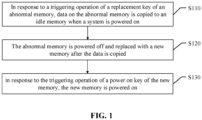
FIG. 1 schematically illustrates a flowchart of a method for hot swapping a memory according to an exemplary implementation mode of the disclosure. -
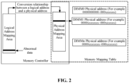
FIG. 2 schematically illustrates a flowchart of determining an abnormal memory from abnormal data according to the exemplary implementation mode of the disclosure. -
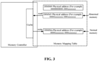
FIG. 3 schematically illustrates a flowchart of copying data on the abnormal memory according to the exemplary implementation mode of the disclosure. -
FIG. 4 schematically shows a flowchart of operations of method for hot swapping a memory according to an exemplary implementation mode of the disclosure. -
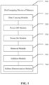
FIG. 5 schematically shows a block diagram of a device for hot swapping a memory according to an exemplary implementation mode of the disclosure. -
FIG. 6 schematically shows a schematic structural diagram I of a memory according to an exemplary implementation mode of the disclosure. -
FIG. 7 schematically shows a schematic structural diagram II of a memory according to an exemplary implementation mode of the disclosure. -
FIG. 8 schematically shows a schematic structural diagram III of a memory according to an exemplary implementation mode of the disclosure. -
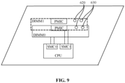
FIG. 9 schematically shows a schematic structural diagram of a mainboard for inserting the abovementioned memory according to an exemplary implementation mode of the disclosure. - Exemplary implementation modes will now be described more comprehensively with reference to the accompanying drawings. However, the exemplary implementation modes can be implemented in a variety of forms and should not be construed as being limited to the examples set forth herein. Instead, these implementation modes are provided, so that the disclosure will be more comprehensive and complete, and the concepts of the exemplary implementation modes are fully conveyed to those skilled in the art. The described features, structures, or characteristics may be combined in one or more implementation modes in any suitable mode. In the following description, numerous specific details are provided for fully understanding the implementation modes of the present disclosure. However, those skilled in art will appreciate that the technical solution of the disclosure may be practiced while omitting one or more of the specific details, or other methods, components, apparatuses, steps, etc. may be employed. In other cases, the well-known technical solutions are not shown or described in detail, so as to avoid obscuring various aspects of the disclosure.
- In addition, the accompanying drawings are merely schematic illustrations of the disclosure and are not necessarily drawn to scale. The same reference numerals in the drawings denote the same or similar parts, so repeated description thereof will be omitted. Some block diagrams shown in the drawings are functional entities and do not necessarily to correspond to physically or logically separate entities. These functional entities may be implemented in form of software, or these functional entities may be implemented in one or more hardware modules or integrated circuits, or these functional entities are implemented in different networks and/or processor apparatuses and/or micro-controller apparatuses.
- The flowcharts shown in the drawings are merely exemplary descriptions and do not necessarily include all of the operations. For example, some of the operations may be divided and some of the steps may be combined or partially combined, so that the order of actual execution may vary depending on actual situations. In addition, all the following terms "first", "second" and "third" are for the purpose of distinction only and should not be used as a limitation of the disclosure.
- DDR4 is the abbreviation of the fourth generation DDR SDRAM, DDR5 is the abbreviation of the fifth generation DDR SDRAM, DDR SDRAM is the abbreviation of Double Data Rate SDRAM in English, and SDRAM is the abbreviation of Synchronous Dynamic Random Access Memory. The synchronization object is a system clock frequency. Therefore, in combination, DDR4 is the fourth generation double rate synchronous dynamic random access memory, and DDR5 is the fifth generation double rate synchronous dynamic random access memory. From DDR4 to DDR5, a power supply unit of a DIMM memory has been moved from a mainboard to the DIMM memory. The power supply on each DIMM memory is independent. Therefore, each DIMM memory may be powered on and powered off independently.
- On this basis, the embodiments of the disclosure provide a method for hot swapping a memory, which is applied to a memory that can supply power to a memory module, such as DDR5, independently, thus can replace an abnormal memory without shutting down a system, so as to realize a hot-swap mode of the memory. Referring to
FIG. 1 , the method for hot swapping a memory may include the following operations. - At S110, in response to a triggering operation of a replacement key of an abnormal memory, data on the abnormal memory is copied to an idle memory when a system is powered on.
- At S120, the abnormal memory is powered off and replaced with a new memory after the data is copied.
- At S130, in response to a triggering operation of a power on key of the new memory, the new memory is powered on.
- According to the method for hot swapping a memory provided by exemplary implementation mode of the disclosure, the data on the abnormal memory may be copied to an idle memory first in response to the triggering operation of the replacement key of the abnormal memory when the system is in a working state, and only the abnormal memory is powered off after the data is copied; then, the abnormal memory may be replaced with a new memory; and the new memory may be powered on in response to the triggering operation of the power on key of the new memory. The whole process described above may realize an abnormal memory replacement process when the system is in the working state, that is, a method for hot swapping a memory.
- The abovementioned method for hot swapping the memory is specifically described below in combination with a specific operation process.
- At S 110, the data on the abnormal memory is copied to the idle memory in response to the triggering operation of the replacement key of the abnormal memory when the system is powered on.
- In an exemplary implementation mode of the disclosure, the system may include a computer system or a server system, which is a machine system that receives and stores information according to human requirements, automatically performs data processing and calculation, and outputs result information.
- The system usually needs to store data. Therefore, the system also includes a memory. During working, data may be read from the memory or may be stored in the memory.
- In an exemplary implementation mode of the disclosure, the system in a powered on state may be that the system is in a startup state, or the system is in a working state, for example, a state that the system is performing a data access operation and the like. Here, the system in the powered on state may be understood that the system is not in a shutdown state, and the system does not need to be shut down during the whole swapping process of the memory.
- In actual applications, the abnormal memory may be a memory with a data reading error, that is, abnormal data are found in the abnormal memory. A physical address of the abnormal memory is determined according to the logical address of abnormal data after the abnormal data is found.
- Reference is made to
FIG. 2 , which illustrates a flowchart of determining an abnormal memory from abnormal data. As shown inFIG. 2 , when a memory controller (MC) finds that there is abnormal data in memory data, the MC may acquire the logical address of the abnormal data from a logical address mapping area, and the MC then coverts the logical address of the abnormal data into a physical address of the abnormal memory according to a conversion relationship between the logical address and the physical address, so that a corresponding DIMM memory may be found according to the physical address. InFIG. 2 , a physical address mapping area in the MC corresponds to a memory physical address in a memory mapping table. A specific abnormal memory may be determined from the physical address in the physical address mapping area. - In an exemplary implementation mode of the disclosure, the replacement key may be a physical key arranged on the abnormal memory or a virtual key added on a baseboard management controller (BMC) interface. The replacement key is connected to the CPU of the system through a hub, and thus informs the CPU or the MC through a system management bus (Smbus) or an improved inter integrated circuit (13C) signal, that the corresponding memory needs to be powered off and replaced.
- When a user wants to replace the abnormal memory and after the replacement key is pressed, according to the method for hot swapping the memory provided by the embodiments of the disclosure, first, the data in the abnormal memory may be copied to an idle memory in response to a triggering operation of the replacement key, so as to save the data in the abnormal memory. The triggering operation of the replacement key may be a single-click operation, a double-click operation, a long press operation, or other triggering operations. There are no special limits made to specific forms of the triggering operations in the exemplary implementation mode of the disclosure.
- In an exemplary implementation mode of the disclosure, reference is made to
FIG. 3 which illustrates a flowchart of copying data of the abnormal memory. During copying the data of the abnormal memory, firstly, a writing operation on the abnormal memory needs to be stopped first, and new data is not written into the abnormal memory any longer, so as to prevent data loss. Secondly, the data in the abnormal memory may be read through a reading operation, and the read data may be stored in a cache that can temporarily store the data. Finally, the data in the cache may be written into an idle memory other than the abnormal memory. The idle memory here may be a normal memory that stores some data or a normal memory that does not store any data. - It is to be noted that the abovementioned data copying process of the abnormal memory may be executed by an MC.
- At S120, the abnormal memory is powered off after the data is copied, and the abnormal memory is replaced with a new memory.
- In an exemplary implementation mode of the disclosure, after the data in the abnormal memory is copied to the idle memory, the abnormal memory is powered off. A specific powering off operation may be that the abnormal memory is powered off by pulling down a power management IC enable signal corresponding to the abnormal memory after the CPU or the MC receives the Smbus or the I3C signal. The power management IC enable signal is an enable signal when the power management IC (PMIC) works.
- In actual applications, whether the abnormal memory has been powered off may also be indicated by an indicating lamp. For example, the replacement key is set as a key with a double-color indicating lamp. After the replacement key is pressed down, the color of the indicating lamp changes, which indicates that abnormal memory has been powered off.
- After the abnormal memory is powered off, the abnormal memory may be replaced with a new memory. This process may be operated manually.
- In an exemplary implementation mode of the disclosure, after the abnormal memory is powered off, the record of the abnormal memory further needs to be removed from the memory mapping table of the system, so that the system does not record the abnormal memory any longer. The memory mapping table is a record table that stores the physical addresses of memories. The abnormal memory record usually needs to be removed from the memory mapping table, so that the system can acquire the physical address of a normal memory from the memory mapping table.
- At S130, the new memory is powered on in response to the triggering operation of the power on key of the new memory.
- In an exemplary embodiment of the disclosure, a newly inserted memory needs a triggering operation after the abnormal memory is replaced with the new memory. The triggering operation may be a single-click operation, a double-click operation, a long press operation, or other triggering operations. There are no special limits made to specific forms of the triggering operation in the exemplary embodiment of the disclosure.
- In response to the triggering operation of the power on key of the new memory, the power on key may inform the CPU or the MC to perform power-on initialization of the new memory.
- In an exemplary implementation mode of the disclosure, the power on key may be a physical key arranged on the new memory or a virtual key added on the BMC interface. The power on key is connected to the CPU or the MC of the system through a hub, and informs the CPU or the MC by a Smbus or an I3C signal that the corresponding memory needs to power on.
- A specific powering on operation may be that the new memory is powered on by pulling up a power management IC enable signal corresponding to the new memory after the CPU or the MC receives the Smbus or the I3C signal. The power management IC enable signal is an enable signal when a Power Management IC (PMIC) works.
- In actual applications, whether a new memory has been powered on may also be indicated by an indicating lamp. For example, the power on key is set as a key with a double-color indicating lamp. After the power on key is pressed down, the color of the indicating lamp changes, so as to indicate that the new memory has been powered off.
- In actual applications, after the new memory is powered on, the system also needs to initialize and adjust the new memory to have an optimal state. After that, the system may record the new memory to the memory mapping table of the system for normal use of the system. The initialization and adjustment of the new memory belong to conventional technical means, which will not be elaborated herein.
- According to the method for hot swapping the memory provided by an exemplary implementation mode of the disclosure, an abnormal memory may be powered off and replaced with a new memory after the data on the abnormal memory is copied to an idle memory in response to a triggering operation of a replacement key of the abnormal memory when the system is in a powered on state. That is, it is unnecessary to shut down the system in the replacement process of the abnormal memory, and there is no time spent for shutting down the system in the replacement process, so that the time consumption for replacing the abnormal memory can be reduced. It is convenience for a user with implementation of the hot swap mode for an abnormal memory when the system is powered on or in a working state.
-
FIG. 4 illustrates a flowchart of operations of the method for hot swapping the memory provided by an exemplary implementation mode of the disclosure. As shown inFIG. 4 , first, S401 is entered. When a system is powered on, a replacement key of an abnormal memory is triggered. S402, data on the abnormal memory is copied to an idle memory in response to the triggering operation of the replacement key of the abnormal memory, referred to as data copying for short. S403, a power management IC enable signal is pulled down to power off the abnormal memory after the data is copied. S404, the abnormal memory is replaced with a new memory after the abnormal memory is powered off. S405, a power on key of the new memory is triggered. S406, the new memory is powered on and initialized in response to the triggering operation of the power on key of the new memory. S407, after initialization, the new memory is added to the memory mapping table of the system, so that the new memory can work normally. - In addition, the exemplary implementation mode of the disclosure further provides a device for hot swapping a memory. Referring to
FIG. 5 , thehot swapping device 500 of a memory includes: adata copying module 510, a power offmodule 520, a power onmodule 530, aremoval module 540, anaddition module 550, and anaddress determination module 560. - The
data copying module 510 may be configured to, in response to a triggering operation of a replacement key of the abnormal memory, copy data on an abnormal memory to an idle memory, when a system is powered on. - The power off
module 520 may be configured to power off the abnormal memory and replace the abnormal memory with a new memory after the data is copied. - The power on
module 530 may be configured to, in response to a triggering operation of a power on key of the new memory, power on the new memory. - In an exemplary implementation mode of the disclosure, the power off
module 520 may be configured to pull down a power management IC enable signal corresponding to the abnormal memory to power off the abnormal memory. - In an exemplary implementation mode of the disclosure, the
removal module 540 may be configured to remove the abnormal memory from a memory mapping table of the system. - In an exemplary implementation mode of the disclosure, the
addition module 550 may be configured to add the new memory to the memory mapping table of the system. - In an exemplary implementation mode of the disclosure, the
address determination module 560 may be configured to determine a physical address of the abnormal memory according to a logical address of abnormal data. - In an exemplary implementation mode of the disclosure, the
data copying module 510 may be configured to stop a writing operation on the abnormal memory, store the data in the abnormal memory in a cache through a reading operation, and write the data in the cache into the idle memory. - In an exemplary implementation mode of the disclosure, the power on
module 530 may be configured to pull up a power management IC enable signal corresponding to the new memory to power on the new memory. - Specific details of various modules in the abovementioned hot swapping device of a memory have been described in detail in the corresponding method for hot swapping a memory, which will not be elaborated herein.
- Further, in order to implement the abovementioned method for hot swapping the memory, an exemplary implementation mode of the disclosure further provides a memory capable of applying the method for hot swapping a memory. Referring to
FIG. 6 , the memory includes: amemory body 610, areplacement key 620 and a power onkey 630 arranged on thememory body 610. - The
replacement key 620 and the power onkey 630 are separately connected to a hub HUB640 through an input/output interface IO. Thehub 640 may be configured to send a system management bus signal to a CPU when level conversion occurs at the input/output interface IO. That is to say, thehub 640 needs to be connected with the CPU. The CPU may be an element independent from the memory in the system. - The memory needs to be connected to the CPU through the
hub 640, so as to power on or power off the memory through the CPU. That is, the CPU can power on or power off the memory after receiving the system management bus signal. - In actual applications, the input/output interface IO connected to the
replacement key 620 and the power onkey 630 may be different pins of the same IO IC. One pin is connected to thereplacement key 620 and the other pin is connected to the power onkey 630. - In an exemplary implementation mode of the disclosure, the system management bus signal may include the Smbus or I3C signal described in the foregoing embodiments.
- In an exemplary implementation mode of the disclosure, the level conversion of the input/output interface IO may be that the level at the input/output interface IO is converted from a high level to a low level when the
replacement key 620 is triggered; or the level at the input/output interface IO is converted from a low level to a high level when thereplacement key 620 is triggered. - In addition, the level conversion of the input/output interface IO may also be that the level at the input/output interface IO is converted from a high level to a low level when the power on
key 630 is triggered; or the level at the input/output interface IO is converted from a low level to a high level when the power onkey 630 is triggered. - In order to realize the level conversion at the input/output interface IO, referring to
FIG. 7 , the memory may further include afirst power supply 710 and afirst resistor 720. The input/output interface IO is grounded through thereplacement key 620, and thefirst power supply 710 is arranged on a connecting line between the input/output interface IO and thereplacement key 620 to provide a high level for the input/output interface IO. Thefirst resistor 720 is also arranged on the connecting line of thefirst power supply 710, and thefirst resistor 720 can achieve an effect of stabilizing the voltage. The resistance of thefirst resistor 720 may be set according to actual situations. There are no special limits made thereto in the exemplary implementation mode of the disclosure. - In an exemplary implementation mode of the disclosure, after the
replacement key 620 is pressed down, the input/output interface IO is communicated with a ground terminal, so that the level at the input/output interface IO will be converted from a high level to a low level. As shown inFIG. 7 , the input/output interface IO here may be afirst pin 1 of an IO chip. - In actual applications, the
replacement key 620 may be a switch, and the input/output interface IO and the ground terminal may be conducted when thereplacement key 620 is pressed down. - In an exemplary implementation mode of the disclosure, continuing to refer to
FIG. 7 , the memory may further include asecond power supply 730 and asecond resistor 740. The input/output interface IO is grounded through the power onkey 630, and thesecond power supply 730 is arranged on a connecting line between the input/output interface IO and the power onkey 630 to provide a high level for the input/output interface IO. Thesecond resistor 740 is also arranged on the connecting line of thesecond power supply 730, and thesecond resistor 740 can achieve an effect of stabilizing the voltage. The resistance of thesecond resistor 740 may be set according to actual situations. There are no special limits made thereto in the exemplary implementation mode of the disclosure. - In an exemplary implementation mode of the disclosure, after the power on
key 630 is pressed down, the input/output interface IO is communicated with a ground terminal, so that the level at the input/output interface IO will be converted from a high level to a low level. As shown inFIG. 7 , the input/output interface IO here may be asecond pin 2 of an IO chip. - In actual applications, the power on
key 630 may be a switch, and the input/output interface IO and the ground terminal may be conducted when the power onkey 630 is pressed down. - An exemplary implementation mode of the disclosure further provides an alternative method for realizing level conversion at an input/output interface IO. Referring to
FIG. 8 , the memory may further include athird power supply 810. In the memory, the input/output interface IO is directly grounded to provide a low level for the input/output interface IO. In addition, thereplacement key 620 is arranged between thethird power supply 810 and the input/output interface IO. When thereplacement key 620 is pressed down or triggered, thethird power supply 810 will be conducted with the input/output interface IO, so that the level at the input/output interface IO is converted from a low level to a high level. As shown inFIG. 8 , the input/output interface IO here may be afirst pin 1 of an IO chip. - In practical application, a resistor may or may not be arranged beside the
third power supply 810. There are no special limits made thereto in the exemplary implementation mode of the disclosure. The resistance of the resistor may also be set according to actual situations. There are no limits made thereto herein. - In an exemplary implementation mode of the disclosure, the
replacement key 620 may be a switch, and thethird power supply 810 and the input/output interface IO may be conducted when thereplacement key 620 is pressed down. - In an exemplary implementation mode of the disclosure, continuing to refer to
FIG. 8 , the memory may further include afourth power supply 820. In the memory, since the input/output interface IO is directly grounded, the level at the input/output interface IO is a low level at first. In addition, the power onkey 630 is arranged between thefourth power supply 820 and the input/output interface IO. When the power onkey 630 in pressed down or triggered, thefourth power supply 820 will be conducted with the input/output interface IO, so that the level at the input/output interface IO is converted from a low level to a high level. As shown inFIG. 8 , the input/output interface IO here may be asecond pin 2 of an IO chip. - In an exemplary implementation mode of the disclosure, the abovementioned power on
key 630 may be a switch, and thefourth power supply 820 and the input/output interface IO may be conducted when the power onkey 630 is pressed down. - In an exemplary implementation mode of the disclosure, in order to power on or off the memory through the CPU, as shown in
FIG. 6 , the CPU also needs to be connected to the power management IC PMIC650 of the memory. The CPU can control the memory to be powered off by pulling down the power management IC enable signal; and the CPU can control the memory to be powered on by pulling up the power management IC enable signal. - In an exemplary implementation mode of the disclosure, as shown in
FIG. 7 andFIG. 8 , the input/output interface IO is connected to a connecting finger of the memory through a hub. The hub is connected to the CPU by the connecting finger through the wiring on the mainboard, so as to realize the transmission of signals. - The memory provided by the embodiments of the disclosure may be switched between the power supply and the ground terminal by connecting the input/output interface with the power supply or the ground terminal, thereby realizing the level conversion at the input/output interface. When the level conversion occurs at the input/output interface, the hub can send the system management bus signal to the CPU, and the CPU can power on or power off the memory, so as to realize the power off replacement of the abnormal memory and the power on of the newly replaced memory. That is, the memory can be used in the hot swapping process of the memory described in the abovementioned embodiments.
- Referring to
FIG. 9 , a mainboard for inserting the abovementioned memory is provided. On the mainboard as shown inFIG. 9 , the power supply PMIC of each memory has been disposed on the memory other than the mainboard. Such as DDR5 DIMM, each DIMM has an independent PMIC, so that each DIMM can be powered on and off independently. - In addition, a sub memory controller (SMC) of each channel of the CPU is also independent, and one SMC controls one DIMM. For example, as shown in
FIG. 9 , SMC0 on the CPU controls DIMM0, and SMC1 controls DIMM1. When DIMM0 is replaced, it only needs to be controlled by SMC0. When DIMM1 is replaced, it only needs to be controlled by SMC1. - Therefore, when one of the memories is abnormal and needs to be replaced, only this memory needs to be powered off, which will not affect the normal use of other memories, and the CPU can work normally. Similarly, the newly replaced memory can also be powered on directly without affecting other memories and CPU, thus providing a basis for hot swapping memories.
- The abovementioned embodiments may be completely or partially implemented through software, hardware, firmware, or any combination thereof. When software is used to implement the embodiments, the embodiments may be implemented completely or partially in a form of a computer program product. The computer program product includes one or more computer commands. When the computer program commands are loaded and executed on a computer, the processes or functions according to the embodiments of the disclosure are generated completely or partially. The computer may be a universal computer, a dedicated computer, a computer network, or other programmable apparatuses. The computer commands may be stored in a computer readable storage medium, or may be transmitted from one computer readable storage medium to another. The computer readable storage medium may be any available medium accessible to a computer, or a data storage device, such as a server or a data center, integrating one or more available media. The available medium may be a magnetic medium (such as floppy disk, hard disk, and magnetic tape), an optical medium (such as a DVD), or a semiconductor medium (such as a solid state disk (SSD)). In the embodiments of the disclosure, the computer may include the apparatuses described above.
- Although the disclosure is described with reference to various embodiments here, in a process of implementing the disclosure that claims protection, those skilled in the art may understand and implement other variations of the disclosed embodiments by viewing the accompanying drawings, disclosed content, and the accompanying claims. In claims, "comprising" does not exclude another component or another step, and "a" or "one" does not exclude the case of plurality. A single processor or other units may implement several functions enumerated in the claims. Some measures are described in dependent claims that are different from each other, but this does not mean that these measures cannot be combined to produce a better effect.
- Although the disclosure is described with reference to specific features and the embodiments thereof, apparently, various modifications and combinations may be made to them without departing from the spirit and scope of the disclosure. Correspondingly, the specification and accompanying drawings are merely exemplary descriptions of the disclosure defined by the accompanying claims, and are considered as any or all modifications, variations, combinations or equivalents that cover the scope of the disclosure. Apparently, those skilled in the art can make various modifications and variations to the disclosure without departing from the spirit and scope of the disclosure. The disclosure is also intended to cover these modifications and variations provided that they fall within the scope of protection defined by the claims and their equivalent technologies of the disclosure.
Claims (15)
- A method for hot swapping a memory, comprising:in response to a triggering operation of a replacement key of an abnormal memory, copying data on the abnormal memory to an idle memory when a system is powered on;powering off the abnormal memory, and replacing the abnormal memory with a new memory after the data is copied; andin response to a triggering operation of a power on key of the new memory, powering on the new memory.
- The method of claim 1, wherein the powering off the abnormal memory comprises:
pulling down a power management IC enable signal corresponding to the abnormal memory, so that the abnormal memory is powered off. - The method of claim 1 or 2, further comprising:
removing the abnormal memory from a memory mapping table of the system after powering off the abnormal memory. - The method of claim 1, further comprising:
adding the new memory to the memory mapping table of the system after powering on the new memory. - The method of claim 1, further comprising:
determining a physical address of the abnormal memory according to a logical address of abnormal data. - The method of claim 1, wherein the copying data on the abnormal memory to the idle memory comprises:stopping a writing operation on the abnormal memory, and storing the data in the abnormal memory into a cache by a reading operation; andwriting the data in the cache into the idle memory.
- The method of claim 1, wherein the powering on the new memory comprises:
pulling up the power management IC enable signal corresponding to the new memory to power on the new memory. - A device for hot swapping a memory, comprising:a data copying module configured to, in response to a triggering operation of a replacement key of an abnormal memory, copy data on the abnormal memory to an idle memory when a system is powered on;a power off module configured to power off the abnormal memory and replace the abnormal memory with a new memory after the data is copied; anda power on module configured to, in response to a triggering operation of a power on key of the new memory, power on the new memory .
- A memory, comprising a memory body, and a replacement key and a power on key arranged on the memory body, whereinthe replacement key and the power on key are separately connected to a hub through an input/output interface; and the hub is configured to send a system management bus signal to a central processing unit (CPU) when level conversion occurs at the input/output interface; andthe CPU is configured to power on or power off the memory after receiving the system management bus signal.
- The memory of claim 9, further comprising a first power supply and a first resistor, wherein
the input/output interface is grounded through the replacement key; the first power supply is arranged on a connecting line between the input/output interface and the replacement key; and the first resistor is arranged on a connecting line of the first power supply. - The memory of claim 9, further comprising a second power supply and a second resistor, wherein
the input/output interface is grounded through the power on key; the second power supply is arranged on the connecting line between the input/output interface and the power on key; and the second resistor is arranged on a connecting line of the second power supply. - The memory of claim 9, further comprising a third power supply, wherein
the input/output interface is grounded; and the replacement key is arranged between the third power supply and the input/output interface. - The memory of claim 9, further comprising a fourth power supply, wherein
the input/output interface is grounded; and the power on key is arranged between the fourth power supply and the input/output interface. - The memory of any one of claims 9 to 13, wherein both the power on key and the replacement key are switches.
- The memory of claim 9, wherein the CPU is connected to the power management IC of the memory; the CPU controls the memory to be powered off by pulling down the power management IC enable signal; and
the CPU controls the memory to be powered on by pulling up the power management IC enable signal.
Applications Claiming Priority (2)
| Application Number | Priority Date | Filing Date | Title |
|---|---|---|---|
| CN202210550689.XA CN114780473A (en) | 2022-05-18 | 2022-05-18 | Memory bank hot plug method and device and memory bank |
| PCT/CN2022/099681 WO2023221227A1 (en) | 2022-05-18 | 2022-06-20 | Hot plugging method and apparatus for memory module, and memory module |
Publications (2)
| Publication Number | Publication Date |
|---|---|
| EP4300319A1 true EP4300319A1 (en) | 2024-01-03 |
| EP4300319A4 EP4300319A4 (en) | 2024-02-28 |
Family
ID=88791508
Family Applications (1)
| Application Number | Title | Priority Date | Filing Date |
|---|---|---|---|
| EP22760642.3A Withdrawn EP4300319A4 (en) | 2022-05-18 | 2022-06-20 | HOT PLUGGING METHOD AND APPARATUS FOR MEMORY MODULE, AND MEMORY MODULE |
Country Status (4)
| Country | Link |
|---|---|
| US (1) | US12008245B2 (en) |
| EP (1) | EP4300319A4 (en) |
| JP (1) | JP2024523768A (en) |
| KR (1) | KR20230161864A (en) |
Families Citing this family (1)
| Publication number | Priority date | Publication date | Assignee | Title |
|---|---|---|---|---|
| KR20240098462A (en) * | 2022-12-21 | 2024-06-28 | 삼성전자주식회사 | Memory expander and computing system including the same |
Family Cites Families (43)
| Publication number | Priority date | Publication date | Assignee | Title |
|---|---|---|---|---|
| JPH02139610A (en) * | 1988-11-19 | 1990-05-29 | Fujitsu Ltd | Active attaching and detaching system |
| JP3561002B2 (en) * | 1994-05-18 | 2004-09-02 | 富士通株式会社 | Disk unit |
| US6038680A (en) | 1996-12-11 | 2000-03-14 | Compaq Computer Corporation | Failover memory for a computer system |
| US6487623B1 (en) | 1999-04-30 | 2002-11-26 | Compaq Information Technologies Group, L.P. | Replacement, upgrade and/or addition of hot-pluggable components in a computer system |
| JP2001167001A (en) * | 1999-10-28 | 2001-06-22 | Hewlett Packard Co <Hp> | Self-recovery memory configuration |
| FR2808903A1 (en) | 2000-05-12 | 2001-11-16 | Ibm | MEMORY ACCESS SYSTEM |
| US7076686B2 (en) | 2002-02-20 | 2006-07-11 | Hewlett-Packard Development Company, L.P. | Hot swapping memory method and system |
| JP4072424B2 (en) * | 2002-12-02 | 2008-04-09 | エルピーダメモリ株式会社 | Memory system and control method thereof |
| US6959370B2 (en) | 2003-01-03 | 2005-10-25 | Hewlett-Packard Development Company, L.P. | System and method for migrating data between memories |
| JP4065790B2 (en) * | 2003-01-17 | 2008-03-26 | 三菱電機株式会社 | In-vehicle electronic control unit |
| JP4274140B2 (en) * | 2005-03-24 | 2009-06-03 | 日本電気株式会社 | Memory system with hot swap function and replacement method of faulty memory module |
| US7350089B2 (en) | 2005-06-28 | 2008-03-25 | Intel Corporation | System for memory hot swap |
| US8612797B2 (en) * | 2006-03-31 | 2013-12-17 | Hewlett-Packard Development Company, L.P. | Systems and methods of selectively managing errors in memory modules |
| JP2009054116A (en) * | 2007-08-29 | 2009-03-12 | Buffalo Inc | Memory system and information processing apparatus |
| JP4578542B2 (en) * | 2008-07-02 | 2010-11-10 | 三菱電機株式会社 | In-vehicle electronic control unit |
| KR101026874B1 (en) * | 2008-11-20 | 2011-04-06 | 한전케이피에스 주식회사 | Deviation measuring system of rotation axis by wireless method |
| WO2011007599A1 (en) * | 2009-07-17 | 2011-01-20 | 株式会社 東芝 | Memory management device |
| TWI450184B (en) | 2009-11-30 | 2014-08-21 | Yang Chang Lien Ou | Hot swap method for dram |
| CN202615294U (en) | 2012-04-20 | 2012-12-19 | 浪潮电子信息产业股份有限公司 | Hot inserting-pulling type internal memory board |
| CN103019978B (en) * | 2012-12-31 | 2015-08-12 | 中国矿业大学(北京) | Based on intelligent trigger device and the control method thereof of embedded system |
| CN103198028B (en) * | 2013-03-18 | 2015-12-23 | 华为技术有限公司 | A kind of internal storage data moving method, Apparatus and system |
| CN104423489A (en) * | 2013-09-02 | 2015-03-18 | 鸿富锦精密电子(天津)有限公司 | Memory hot-plugging type mainboard |
| ES2612829T3 (en) * | 2013-11-22 | 2017-05-18 | Huawei Technologies Co., Ltd. | Computer and memory data migration method |
| WO2015074232A1 (en) * | 2013-11-22 | 2015-05-28 | 华为技术有限公司 | Method for migrating memory data, computer and device |
| CN105353980B (en) | 2013-11-22 | 2019-10-22 | 华为技术有限公司 | Method, computer and device for migrating memory data |
| US20150363309A1 (en) * | 2014-06-17 | 2015-12-17 | Kingtiger Technology (Canada) Inc. | System and method of increasing reliability of non-volatile memory storage |
| WO2016115661A1 (en) | 2015-01-19 | 2016-07-28 | 华为技术有限公司 | Memory fault isolation method and device |
| US9904627B2 (en) * | 2015-03-13 | 2018-02-27 | International Business Machines Corporation | Controller and method for migrating RDMA memory mappings of a virtual machine |
| US20170031399A1 (en) * | 2015-07-28 | 2017-02-02 | Hong Fu Jin Precision Industry (Shenzhen) Co., Ltd | Motherboard with multiple chips |
| TWI575374B (en) | 2015-08-04 | 2017-03-21 | 群聯電子股份有限公司 | Mapping table updating method, memory storage device and memory control circuit unit |
| US10397386B1 (en) * | 2015-08-18 | 2019-08-27 | Marvell International Ltd. | System and method for providing test scenario reproduction for a device under test |
| DE102016201531A1 (en) | 2016-02-02 | 2017-08-03 | Robert Bosch Gmbh | Method and device for detecting fatigue of a driver |
| US10268612B1 (en) * | 2016-09-23 | 2019-04-23 | Amazon Technologies, Inc. | Hardware controller supporting memory page migration |
| KR20180085192A (en) | 2017-01-18 | 2018-07-26 | 에스케이하이닉스 주식회사 | System including hot plug module and memory module |
| CN109302188A (en) | 2017-07-25 | 2019-02-01 | 厦门雅迅网络股份有限公司 | Detection method and circuit of a resistance-divided wire-controlled button |
| US10374649B2 (en) * | 2017-12-21 | 2019-08-06 | Randy Mark Cunningham | Device and method of verifying protective case usage |
| CN111143898B (en) | 2018-11-05 | 2022-06-14 | 瑞昱半导体股份有限公司 | Data protection method for pluggable memory device |
| CN110347531A (en) | 2019-07-05 | 2019-10-18 | 湖南省华芯医疗器械有限公司 | A kind of machine hot plug working method and system avoiding loss of data |
| CN110580195B (en) | 2019-08-29 | 2023-11-07 | 上海仪电(集团)有限公司中央研究院 | Memory allocation method and device based on memory hot plug |
| US11620233B1 (en) * | 2019-09-30 | 2023-04-04 | Amazon Technologies, Inc. | Memory data migration hardware |
| US11461263B2 (en) * | 2020-04-06 | 2022-10-04 | Samsung Electronics Co., Ltd. | Disaggregated memory server |
| DE102020207616A1 (en) * | 2020-06-19 | 2021-12-23 | Robert Bosch Gesellschaft mit beschränkter Haftung | Method for operating a computing unit |
| KR20230008470A (en) * | 2021-07-07 | 2023-01-16 | 에스케이하이닉스 주식회사 | A memory module substrate and a method of operating a memory module substrate using the same |
-
2022
- 2022-06-20 KR KR1020227039437A patent/KR20230161864A/en not_active Ceased
- 2022-06-20 JP JP2022562319A patent/JP2024523768A/en active Pending
- 2022-06-20 EP EP22760642.3A patent/EP4300319A4/en not_active Withdrawn
- 2022-08-23 US US17/821,760 patent/US12008245B2/en active Active
Also Published As
| Publication number | Publication date |
|---|---|
| US20230376213A1 (en) | 2023-11-23 |
| EP4300319A4 (en) | 2024-02-28 |
| JP2024523768A (en) | 2024-07-02 |
| KR20230161864A (en) | 2023-11-28 |
| US12008245B2 (en) | 2024-06-11 |
Similar Documents
| Publication | Publication Date | Title |
|---|---|---|
| TWI830373B (en) | Method and device for hot swapping memory, and memory | |
| US20210271624A1 (en) | Apparatuses and methods for selective communication through a memory connector | |
| US6487623B1 (en) | Replacement, upgrade and/or addition of hot-pluggable components in a computer system | |
| US6016518A (en) | Automatic master/slave designation for computer peripherals | |
| US6295591B1 (en) | Method of upgrading and/or servicing memory without interrupting the operation of the system | |
| TWI840849B (en) | Computing system, computer-implemented method, and computer-program product | |
| CN102662903A (en) | Method for realizing hot-plug of PCIE equipment by CPLD or FPGA | |
| CN112908383A (en) | Storage device and data backup method thereof | |
| JP2004295885A (en) | Computer system permitting dynamic reallocation of main memory | |
| US20180203816A1 (en) | System including hot plug module and memory module | |
| US11487638B2 (en) | Computer program product and method and apparatus for controlling access to flash memory card | |
| WO2024103829A1 (en) | Port configuration method, component, and hard disk expansion apparatus | |
| TW202319917A (en) | A computing system, a computer-implemented method and a computer-program product | |
| CN110830563A (en) | Master-slave architecture server and information reading and writing method thereof | |
| US12008245B2 (en) | Method and device for hot swapping memory, and memory | |
| JPH0760421B2 (en) | Computer system with local memory expansion capability | |
| US10140235B2 (en) | Server | |
| CN116841927A (en) | computing equipment | |
| WO2025214078A1 (en) | Computing device and control method | |
| US7127621B2 (en) | Peer power control | |
| US9836359B2 (en) | Storage and control method of the same | |
| CN112286476A (en) | Dual-BMC management system of mainboard | |
| US12026373B2 (en) | System and method to control temperature in a memory device | |
| WO2007149317A2 (en) | Systems and methods for providing a personal computer with non-volatile system memory | |
| CN117632807A (en) | Storage device connection device and connection method and system thereof |
Legal Events
| Date | Code | Title | Description |
|---|---|---|---|
| STAA | Information on the status of an ep patent application or granted ep patent |
Free format text: STATUS: UNKNOWN |
|
| STAA | Information on the status of an ep patent application or granted ep patent |
Free format text: STATUS: THE INTERNATIONAL PUBLICATION HAS BEEN MADE |
|
| PUAI | Public reference made under article 153(3) epc to a published international application that has entered the european phase |
Free format text: ORIGINAL CODE: 0009012 |
|
| STAA | Information on the status of an ep patent application or granted ep patent |
Free format text: STATUS: REQUEST FOR EXAMINATION WAS MADE |
|
| 17P | Request for examination filed |
Effective date: 20220905 |
|
| AK | Designated contracting states |
Kind code of ref document: A1 Designated state(s): AL AT BE BG CH CY CZ DE DK EE ES FI FR GB GR HR HU IE IS IT LI LT LU LV MC MK MT NL NO PL PT RO RS SE SI SK SM TR |
|
| A4 | Supplementary search report drawn up and despatched |
Effective date: 20240131 |
|
| RIC1 | Information provided on ipc code assigned before grant |
Ipc: G06F 11/00 20060101ALI20240125BHEP Ipc: G06F 1/26 20060101ALI20240125BHEP Ipc: G06F 1/18 20060101ALI20240125BHEP Ipc: G06F 11/16 20060101ALI20240125BHEP Ipc: G06F 13/40 20060101AFI20240125BHEP |
|
| STAA | Information on the status of an ep patent application or granted ep patent |
Free format text: STATUS: THE APPLICATION HAS BEEN WITHDRAWN |
|
| 18W | Application withdrawn |
Effective date: 20240812 |