EP4300179A1 - Mini led diffuser, preparation process therefor, and backlighting module - Google Patents
Mini led diffuser, preparation process therefor, and backlighting module Download PDFInfo
- Publication number
- EP4300179A1 EP4300179A1 EP22770184.4A EP22770184A EP4300179A1 EP 4300179 A1 EP4300179 A1 EP 4300179A1 EP 22770184 A EP22770184 A EP 22770184A EP 4300179 A1 EP4300179 A1 EP 4300179A1
- Authority
- EP
- European Patent Office
- Prior art keywords
- diffuser
- filling
- mini led
- led diffuser
- microlens
- Prior art date
- Legal status (The legal status is an assumption and is not a legal conclusion. Google has not performed a legal analysis and makes no representation as to the accuracy of the status listed.)
- Withdrawn
Links
- 238000002360 preparation method Methods 0.000 title description 2
- 238000011049 filling Methods 0.000 claims abstract description 87
- 239000000463 material Substances 0.000 claims abstract description 82
- 239000011324 bead Substances 0.000 claims abstract description 44
- 238000004519 manufacturing process Methods 0.000 claims abstract description 29
- 239000000758 substrate Substances 0.000 claims abstract description 22
- 238000009826 distribution Methods 0.000 claims abstract description 9
- 230000007423 decrease Effects 0.000 claims abstract description 5
- 238000009792 diffusion process Methods 0.000 claims description 44
- 239000002245 particle Substances 0.000 claims description 26
- 239000011347 resin Substances 0.000 claims description 23
- 229920005989 resin Polymers 0.000 claims description 23
- 238000001816 cooling Methods 0.000 claims description 8
- 238000000465 moulding Methods 0.000 claims description 8
- 229920000620 organic polymer Polymers 0.000 claims description 7
- 239000002861 polymer material Substances 0.000 claims description 7
- 239000002131 composite material Substances 0.000 claims description 6
- XAGFODPZIPBFFR-UHFFFAOYSA-N aluminium Chemical compound [Al] XAGFODPZIPBFFR-UHFFFAOYSA-N 0.000 claims description 5
- 239000002096 quantum dot Substances 0.000 claims description 5
- 239000007787 solid Substances 0.000 claims description 5
- 238000002156 mixing Methods 0.000 claims description 4
- 229910052709 silver Inorganic materials 0.000 claims description 4
- 239000004332 silver Substances 0.000 claims description 4
- 238000000576 coating method Methods 0.000 claims description 3
- 239000011248 coating agent Substances 0.000 claims description 2
- 238000002844 melting Methods 0.000 claims description 2
- 230000008018 melting Effects 0.000 claims description 2
- 238000002834 transmittance Methods 0.000 abstract description 15
- 238000005516 engineering process Methods 0.000 abstract description 9
- 238000000206 photolithography Methods 0.000 abstract description 5
- 230000002708 enhancing effect Effects 0.000 abstract 1
- 238000010586 diagram Methods 0.000 description 21
- 230000000694 effects Effects 0.000 description 13
- 238000001125 extrusion Methods 0.000 description 11
- PXHVJJICTQNCMI-UHFFFAOYSA-N Nickel Chemical compound [Ni] PXHVJJICTQNCMI-UHFFFAOYSA-N 0.000 description 4
- 238000001459 lithography Methods 0.000 description 4
- 229920003229 poly(methyl methacrylate) Polymers 0.000 description 4
- 239000004926 polymethyl methacrylate Substances 0.000 description 4
- 239000011521 glass Substances 0.000 description 3
- 229910052751 metal Inorganic materials 0.000 description 3
- 239000002184 metal Substances 0.000 description 3
- 229920002120 photoresistant polymer Polymers 0.000 description 3
- RYGMFSIKBFXOCR-UHFFFAOYSA-N Copper Chemical compound [Cu] RYGMFSIKBFXOCR-UHFFFAOYSA-N 0.000 description 2
- 238000004220 aggregation Methods 0.000 description 2
- 230000002776 aggregation Effects 0.000 description 2
- 230000005540 biological transmission Effects 0.000 description 2
- 229910052802 copper Inorganic materials 0.000 description 2
- 239000010949 copper Substances 0.000 description 2
- 230000002349 favourable effect Effects 0.000 description 2
- 239000007769 metal material Substances 0.000 description 2
- 239000000203 mixture Substances 0.000 description 2
- 239000012768 molten material Substances 0.000 description 2
- 229910052759 nickel Inorganic materials 0.000 description 2
- 230000003287 optical effect Effects 0.000 description 2
- 238000001259 photo etching Methods 0.000 description 2
- 230000002035 prolonged effect Effects 0.000 description 2
- 230000000007 visual effect Effects 0.000 description 2
- 229910000831 Steel Inorganic materials 0.000 description 1
- 239000000853 adhesive Substances 0.000 description 1
- 238000004026 adhesive bonding Methods 0.000 description 1
- 230000001070 adhesive effect Effects 0.000 description 1
- 229910052782 aluminium Inorganic materials 0.000 description 1
- 230000009286 beneficial effect Effects 0.000 description 1
- 230000015572 biosynthetic process Effects 0.000 description 1
- 230000008859 change Effects 0.000 description 1
- 229910003460 diamond Inorganic materials 0.000 description 1
- 239000010432 diamond Substances 0.000 description 1
- 238000005323 electroforming Methods 0.000 description 1
- 230000006872 improvement Effects 0.000 description 1
- 230000031700 light absorption Effects 0.000 description 1
- 239000007788 liquid Substances 0.000 description 1
- 238000000034 method Methods 0.000 description 1
- 230000004044 response Effects 0.000 description 1
- 238000007790 scraping Methods 0.000 description 1
- 238000007493 shaping process Methods 0.000 description 1
- 229910001220 stainless steel Inorganic materials 0.000 description 1
- 239000010935 stainless steel Substances 0.000 description 1
- 239000010959 steel Substances 0.000 description 1
- 238000010023 transfer printing Methods 0.000 description 1
- XLYOFNOQVPJJNP-UHFFFAOYSA-N water Substances O XLYOFNOQVPJJNP-UHFFFAOYSA-N 0.000 description 1
Images







Classifications
-
- G—PHYSICS
- G02—OPTICS
- G02B—OPTICAL ELEMENTS, SYSTEMS OR APPARATUS
- G02B5/00—Optical elements other than lenses
- G02B5/02—Diffusing elements; Afocal elements
- G02B5/0205—Diffusing elements; Afocal elements characterised by the diffusing properties
- G02B5/021—Diffusing elements; Afocal elements characterised by the diffusing properties the diffusion taking place at the element's surface, e.g. by means of surface roughening or microprismatic structures
- G02B5/0226—Diffusing elements; Afocal elements characterised by the diffusing properties the diffusion taking place at the element's surface, e.g. by means of surface roughening or microprismatic structures having particles on the surface
-
- G—PHYSICS
- G02—OPTICS
- G02B—OPTICAL ELEMENTS, SYSTEMS OR APPARATUS
- G02B3/00—Simple or compound lenses
- G02B3/0006—Arrays
- G02B3/0012—Arrays characterised by the manufacturing method
- G02B3/0031—Replication or moulding, e.g. hot embossing, UV-casting, injection moulding
-
- G—PHYSICS
- G02—OPTICS
- G02B—OPTICAL ELEMENTS, SYSTEMS OR APPARATUS
- G02B3/00—Simple or compound lenses
- G02B3/0006—Arrays
- G02B3/0037—Arrays characterized by the distribution or form of lenses
- G02B3/0056—Arrays characterized by the distribution or form of lenses arranged along two different directions in a plane, e.g. honeycomb arrangement of lenses
-
- G—PHYSICS
- G02—OPTICS
- G02B—OPTICAL ELEMENTS, SYSTEMS OR APPARATUS
- G02B5/00—Optical elements other than lenses
- G02B5/02—Diffusing elements; Afocal elements
- G02B5/0205—Diffusing elements; Afocal elements characterised by the diffusing properties
- G02B5/021—Diffusing elements; Afocal elements characterised by the diffusing properties the diffusion taking place at the element's surface, e.g. by means of surface roughening or microprismatic structures
- G02B5/0215—Diffusing elements; Afocal elements characterised by the diffusing properties the diffusion taking place at the element's surface, e.g. by means of surface roughening or microprismatic structures the surface having a regular structure
-
- G—PHYSICS
- G02—OPTICS
- G02B—OPTICAL ELEMENTS, SYSTEMS OR APPARATUS
- G02B5/00—Optical elements other than lenses
- G02B5/02—Diffusing elements; Afocal elements
- G02B5/0205—Diffusing elements; Afocal elements characterised by the diffusing properties
- G02B5/021—Diffusing elements; Afocal elements characterised by the diffusing properties the diffusion taking place at the element's surface, e.g. by means of surface roughening or microprismatic structures
- G02B5/0221—Diffusing elements; Afocal elements characterised by the diffusing properties the diffusion taking place at the element's surface, e.g. by means of surface roughening or microprismatic structures the surface having an irregular structure
-
- G—PHYSICS
- G02—OPTICS
- G02B—OPTICAL ELEMENTS, SYSTEMS OR APPARATUS
- G02B5/00—Optical elements other than lenses
- G02B5/02—Diffusing elements; Afocal elements
- G02B5/0205—Diffusing elements; Afocal elements characterised by the diffusing properties
- G02B5/021—Diffusing elements; Afocal elements characterised by the diffusing properties the diffusion taking place at the element's surface, e.g. by means of surface roughening or microprismatic structures
- G02B5/0231—Diffusing elements; Afocal elements characterised by the diffusing properties the diffusion taking place at the element's surface, e.g. by means of surface roughening or microprismatic structures the surface having microprismatic or micropyramidal shape
-
- G—PHYSICS
- G02—OPTICS
- G02B—OPTICAL ELEMENTS, SYSTEMS OR APPARATUS
- G02B5/00—Optical elements other than lenses
- G02B5/02—Diffusing elements; Afocal elements
- G02B5/0268—Diffusing elements; Afocal elements characterized by the fabrication or manufacturing method
Definitions
- the present invention relates to the technical field of backlight display, and in particular, to a mini LED diffuser, a manufacturing process therefor, and a backlight module.
- a mini LED array serves as a light source of a backlight module, and has broad application prospects in display industries such as televisions, computers, mobile phones, and vehicles.
- a size of a mini LED chip is generally in a range of 100 ⁇ m to 500 ⁇ m.
- the mini LED chip is mainly used in a direct-lit backlight display system, and has advantages such a little size, a higher brightness, and higher response speed, and is partly adjustable compared to a traditional LED light source.
- a divergence angle of light emitted by a single mini LED point light source is limited, resulting in a higher energy in a central area of a light emergence surface compared to surrounding areas.
- distances between mini LED chips are in a range of 1 mm to 4 mm. Therefore, an array light formed by a plurality of mini LED chips causes light and dark areas to alternately occur on a screen, which results in a poor visual effect and affects user experience.
- a light emergence surface of the mini LED chip is usually covered with a diffusion film based on diffusion particles, to achieve light diffusion and mixing, thereby implementing uniform light emission from the light emergence surface.
- a light mixing distance corresponding to the manner is in a range of a few millimeters to a few centimeters, which does not meet a future requirement on thinning in the display industry.
- structures on two sides of the light homogenizer are in the shape of a pyramid, a prism, or an orthogonal cylinder, which are machined by a diamond lathe. At least two layers of films are required for the light homogenizer to achieve a uniform light, and the films need to be aligned and orthogonally stacked, which is very inconvenient when assembling a backlight module.
- glass beads are collated on a substrate of the light homogenizer to form protruding and recessed points. Since an optical adhesive is used during the formation, a transmittance of the light homogenizer is affected.
- a composite film obtained by gluing two light equalization films each having a prism or glass bead structure on a single surface is used. The composite film has a relatively large thickness, and is not suitable for an ultra-thin device.
- One purpose of the present invention is to provide a mini LED diffuser that can realize a high transmittance while ensuring a high haze. Moreover, arrangement of microstructures, such as microlenses, is particularly designed, and a superposed photolithography technology is used, to overcome a positioning error of a laser head of a lithography machine, thereby ensuring high quality and a high yield. A manufacturing process for the mini LED diffuser and a backlight module using the mini LED diffuser are further provided.
- the diffuser herein may alternatively be referred to as a diffusion film when a thickness thereof is relatively small.
- the diffuser and the diffusion film are collectively referred to as a diffuser.
- the present invention provides a mini LED diffuser, comprising a substrate, a plurality of microstructures disposed on one side of the substrate, and a filling structure disposed on the other side of the substrate.
- the microstructures comprises a plurality of microlens structures and/or a plurality of convex lenses
- the filling structure comprises a plurality of structural units
- each structural unit comprises a plurality of filling patterns distributed based on equal density lines, and a distribution density of the filling patterns in one structural unit gradually decreases from a center of the one structural unit toward a periphery.
- Each of the filling patterns is a groove structure, and each of the filling patterns is filled with a reflective material.
- each of the microlens structures comprises a recessed structure and/or a protrusion structure
- the plurality of microlens structures are arranged in a plurality of rows
- the plurality of microlens structures in two adjacent rows are arranged in an staggered, random, or orthogonal manner
- two adjacent microlens structures partially overlap
- a protruding surface of the protrusion structure is a curved surface
- a recessed surface of the recessed structure is a curved surface.
- a size of each microlens structure is in a range of 0.03 mm to 0.09 mm, and a depth or a height of each microlens structure is in a range of 0.01 mm to 0.05 mm.
- a thickness of the substrate is in a range of 0.1 mm to 2.0 mm, and a range of overlapping between two adjacent microlens structures is 5% to 25%.
- each of the convex lenses is in a shape of one or more of a prism, a pyramid, a semi-cylinder, and a cone, or is in a composite shape composed of one or more of the prism, the pyramid, the semi-cylinder, and the cone according to a set rule.
- each convex lens is in a range of 0.01 mm to 0.1 mm, and when the convex lens is in the shape of a cone, a cone angle thereof is in a range of 60 degrees to 120 degrees
- each of the filling patterns is in a shape of a cylindrical counterbore, and a groove bottom of the filling pattern is in a shape of a circular arc
- the reflective material is one or a combination of reflective ink, metallic silver, and metallic aluminum
- a size of each filling pattern is in a range of 0.005 mm to 0.1 mm, and a depth of each filling pattern is in a range of 0.004 mm to 0.05 mm.
- the present invention further provides a manufacturing process for the foregoing mini LED diffuser, comprising: providing two mold rollers, wherein a plurality of first patterned structures corresponding to shapes of the microstructures are disposed on a surface of one of the mold rollers, adjacent first patterned structures partially overlap, and a plurality of second patterned structures corresponding to shapes of the filling patterns are disposed on a surface of the other of the mold rollers; impressing or extruding a material for forming the mini LED diffuser to obtain a semi-finished diffuser having the microstructures and the filling structure on both sides thereof respectively; and filling the filling structure with a reflective material and obtaining the mini LED diffuser by curing and molding.
- the material for forming the diffuser comprises diffusion particles and a transparent organic polymer material
- the manufacturing process further comprises: mixing the diffusion particles and the transparent organic polymer material and then melting same to a molten state; extruding the melted material through a flow channel formed between the two mold rollers; obtaining the semi-finished diffuser having the microstructures and the filling structure on both sides thereof respectively after cooling and curing; and filling the filling structure with the reflective material and obtaining the mini LED diffuser by curing and molding.
- the material for forming the diffuser comprises a base material layer and a UV-cured resin
- the manufacturing process further comprises: uniformly coating the UV-cured resin on a surface of the base material layer; attaching the mold rollers with the patterned structures to the base material layer coated with the UV-cured resin, curing a UV-cured resin layer on the surface of the base material layer, and forming a solid UV-cured resin layer on the surface of the base material layer, to obtain the semi-finished diffuser having the microstructures and the filling structure on both sides thereof respectively; and filling the filling structure with the reflective material and obtaining the mini LED diffuser by curing and molding
- the present invention provides a backlight module, comprising the foregoing mini LED diffuser.
- the backlight module further comprises a lamp bead panel, a blue light film, a quantum dot film, a first brightness enhancement film, a second brightness enhancement film, and a diffusion film disposed in sequence, wherein the mini LED diffuser is disposed between the lamp bead panel and the blue light film, at least one layer of mini LED diffuser is disposed, the side of the mini LED diffuser filled with the reflective material faces the lamp bead panel, and each of the structural units on the mini LED diffuser corresponds one of lamp beads on the lamp bead panel.
- a mini LED diffuser is provided according to an embodiment I of the prensent invention.
- the mini LED diffuser comprises a substrate 121, a plurality of microlens structures 122 located on one side of the substrate 121, and a filling structure located on the other side of the substrate 121.
- each of the microlens structures 122 shown in the figure is a circular recessed structure 1221.
- a recessed surface of the microlens structure 122 is preferably a curved surface.
- the plurality of microlens structures 122 are arranged in a plurality of rows.
- the plurality of microlens structures 122 in two adjacent rows are arranged in a staggered manner, as shown in FIG.
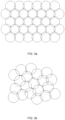
- FIG. 3a or arranged in a random manner, as shown in FIG. 3b , or arranged in an orthogonal manner, as shown in FIG. 3c .
- Two adjacent microlens structures 122 partially overlap, as shown in FIG. 3a to FIG. 3c and FIG. 4 .
- a range of overlapping between two adjacent microlens structures 122 is 5% to 25%, and preferably, is 10%.
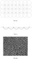
- the design of partial overlapping between two adjacent microlens structures 122 can not only effectively increase a coverage range of the microlens structures 122 on the diffuser, so that a proportion of occupied space can reach 100%, as shown in FIG. 5a and FIG. 5b , but also overcome a positioning error of a laser head of a lithography machine.
- the diffusion effect of the diffuser relates to a radius of curvature and a size of the microlens structure 122.
- the size of the microlens structure 122 is in a range of 0.03 mm to 0.09 mm, a depth is in a range of 0.01 mm to 0.05 mm, and the radius of curvature is in a range of 0.06 mm to 0.2 mm.
- the foregoing relevant parameter ranges of the microlens structure 122 are a preferred range of the present application.
- the relevant parameters of the microlens structure 122 may be designed as required.
- the filling structure comprises a plurality of structural units.
- the structural units comprise a plurality of filling patterns 123 distributed based on equal density lines.
- the distribution density of the plurality of filling patterns 123 in one structural unit gradually decrease from a center of the one structural unit toward a periphery.
- the filling patterns 123 are distributed non-uniformly on the diffuser. Some areas have the filling patterns 123 distributed at a relatively large density, and some areas have the filling patterns distributed at a relatively small density.
- the distribution density of the filling patterns 123 adjacent to a center is greater than the distribution density of the filling patterns 123 away from the center (that is, away from the lamp beads 111).
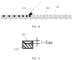
- Each of the plurality of filling patterns 123 is a groove structure, and the filling pattern 123 is filled with a reflective material 1231, as shown in FIG. 10 .
- the filling pattern 123 is in the shape of a cylindrical counterbore, and a groove bottom of the filling pattern 123 is in the shape of a circular arc.
- a sectional shape thereof is circular, square, or any other shape, and preferably, is circular.
- a size of the groove structure is in a range of 0.005 mm to 0.1 mm, and a depth of the groove structure is in a range of 0.004 mm to 0.05 mm.
- the filling pattern 123 in the shape of the cylindrical counterbore can ensure that the reflective material 1231 can be perfectly filled into the filling pattern 123 when the reflective material 1231 is scraped and coated, thereby effectively avoiding a failure in filling the reflective material 1231 or removal of the reflective material during the scraping and coating process.
- the reflective material 1231 is one of reflective ink, metallic silver, and metallic aluminum, but is not limited thereto.
- the reflective material may be another reflective material, or may be a mixture of a plurality of reflective materials.
- the reflective material is preferably reflective ink.
- the reflective material 1231 is configured to reflect light. Light reflected by the reflective material 1231 can be reflected to the diffuser via a lamp bead panel 11. In this way, light energy is fully utilized, and overall uniformity of light can be increased.
- the reflective material 1231 formed by a mixture of reflective ink with metallic silver or metallic aluminum is an existing material. During filling, volatile components such as water are added to the reflective material 1231.
- a middle position of the reflective material 1231 in each filling pattern 123 is recessed inwardly by approximately 1 ⁇ m to 2 ⁇ m, forming a recessed surface on outside of the reflective material 1231, as shown in FIG. 11 .
- the recessed surface can effectively change a propagation direction of light emitted by the lamp beads 111, which improves a diffusion effect of the diffuser on the light emitted by the lamp beads 111.
- high-intensity light adjacent to the lamp beads 111 has a poor light transmission effect and a favorable light diffusion effect when passing through the filling patterns 123 with a relatively high aggregation coefficient
- low-intensity light away from the lamp beads 111 has a favorable light transmission effect and a poor light diffusion effect when passing through the filling patterns 123 with a relatively low aggregation coefficient.
- the diffuser has higher reflection efficiency at positions adjacent to the lamp beads 111 than positions away from the lamp beads 111, thereby achieving uniform light emission from a surface of the diffuser and eliminating non-uniform brightness of the lamp beads 111.
- an area with filling patterns 123 distributed in a relatively large density corresponds to one lamp bead 111
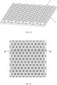
- an area with filling patterns 123 distributed in a relatively small density corresponds to an area between two lamp beads 111, as shown in FIG. 12 . That is to say, a plurality of filling patterns 123 exist at a position on the diffuser corresponding to each lamp bead 111, and the distribution density of the filling patterns 123 decreases with an increase of a distance from the lamp bead 111.
- a thickness of the substrate 121 of the diffuser is in a range of 0.1 mm to 2.0 mm.
- a thicker substrate 121 of the diffuser indicates a larger haze of the diffuser.
- a thinner substrate 121 indicates a higher transmittance of the diffuser.
- two sides of the substrate 121 are respectively provided with the microlens structures 122 and the filling structure, which can not only ensure the haze of the diffuser, but also improve the transmittance of the diffuser. For example, during manufacturing of a relatively thick diffuser (with a thickness greater than 0.6 mm), in order to ensure the haze of the diffuser, diffusion particles are added to a material for manufacturing the diffuser.
- the microlens structures 122 of the present application can reduce a quantity of diffusion particles required to be added during manufacturing of the diffuser, and reduce absorption of light by the diffusion particles, which significantly improves the transmittance of the diffuser while ensuring the haze of the diffuser. It is learned through tests that the haze of the diffuser in the present application can reach 95%, and the transmittance can reach 85%, which is much higher than a transmittance of an existing diffuser in a range of 50% to 60%. The improvement in the transmittance can reduce a demand for a power for a mini LED. In this way, power consumption and to-be-dissipated heat are reduced, a service life of the mini LED is prolonged, and the mini LED is more environmentally friendly.
- a manufacturing process for the foregoing mini LED diffuser is further provided. Specific steps are as follows:
- the diffuser is preferably integrally formed through extrusion, which requires an extrusion device.
- the extrusion device comprises two mold rollers 4 for extrusion.
- the two mold rollers 4 are arranged parallelly and spaced apart from each other.
- An extrusion flow channel is formed between the two mold rollers.
- the first template and the second template are respectively wrapped around outside of the two mold rollers 4, and the patterned structures on the first template and the second template are oriented outward, as shown in FIG. 13 .
- the material for forming the diffuser comprises diffusion particles and a transparent organic polymer material.
- the transparent organic polymer material is any of PET, PC, and PMMA, but is not limited to these materials, which is not enumerated herein.
- the diffusion particles may be PET diffusion particles, PC diffusion particles, or PMMA diffusion particles.
- the diffusion particles are white diffusion particles or yellow diffusion particles, and preferably, are white diffusion particles, but are not limited to these diffusion particles.
- the diffusion particles may also be diffusion particles of another color. Specific manufacturing steps are as follows:
- This embodiment further provides another manufacturing method, which is applicable to manufacturing of a relatively thin diffuser.
- the diffuser herein may alternatively be referred to as a microlens diffusion film when a thickness thereof is relatively small.
- the diffuser and the diffusion film are collectively referred to as a diffuser.
- a material for forming the diffuser in this method comprises a base material layer 5 and a UV-cured resin.
- the base material layer 5 is any of PET, PC, and PMMA, but is not limited to these materials, which is not enumerated herein. As shown in FIG. 14 , specific manufacturing steps are as follows:
- the two sides of the manufactured semi-finished diffuser are respectively provided with the microlens structures 122 and the filling structure. Therefore, during impression, each single side may be impressed independently in sequence, or the two sides may be simultaneously impressed. Principles of the two impression manners are substantially the same, and therefore the details are not described herein.
- the mold roller may be manufactured by attaching a template with a required patterned structure on a surface thereof, or the required patterned structure may be directly manufactured on the surface of the mold roller.
- the template or the mold roller may be made of materials such as nickel, steel, copper, or aluminum.
- This embodiment further provides a backlight module, comprising the foregoing mini LED diffuser 12.
- the backlight module further comprises the lamp bead panel 11, a blue light film 13, a quantum dot film 14, a first brightness enhancement film 15, a second brightness enhancement film 14, and a diffusion film 17 arranged in sequence, as shown in FIG. 15 .
- the diffuser 12 is arranged between the lamp bead panel 11 and the blue light film 13. At least one layer of diffuser 12 is arranged. A side of the diffuser 12 filled with the reflective material 1231 faces the lamp bead panel 11, as shown in FIG. 16 .
- Each of the structural units on the diffuser 12 corresponds one of the lamp beads 111 on the lamp bead panel 11.
- one or more layers of light homogenizers may be added between the blue light film 13 and the diffusion film 17 or between the first brightness enhancement film 15 and the quantum dot film 14 as required.
- the light homogenizers may be provided with the microlens structure 122 on both sides, or may be provided with the microlens structures 122 on one side and a convex lens on the other side, as shown in FIG. 15 .
- microlens structures 122 on one side of the diffuser in this embodiment II is a circular protrusion structure 1222, as shown in FIG. 17 .
- a protruding surface of the microlens structure 122 is preferably a curved surface.
- each convex lens 124 is in the shape of one or more of a prism, a pyramid, a semi-cylinder, and a cone, or is in a composite shape composed of one or more of the shapes according to a set rule.
- the convex lens 124 is in the shape of the prism (such as a triangular prism) or the semi-cylinder, the convex lenses 124 are arranged parallelly and sequentially on a side of the substrate 121, and an axis direction is parallel to the surface where the convex lenses are arranged. Bottom edges of two adjacent convex lenses 124 intersect.
- the convex lens 124 is the shape of the pyramid, for example, a triangular pyramid shown in FIG. 18 to FIG. 21 , or a quadrangular pyramid shown in FIG. 22 to FIG. 25 , or the like, the convex lenses 124 are arranged sequentially. The bottom edges of two adjacent convex lenses 124 intersect, and the two bottom edges staggered each other coincide with a line of intersection, as shown in FIG. 19 or FIG. 23 . Certainly, the convex lens 124 may alternatively be in the shape of another pyramid. This case is substantially the same, and therefore is not described in detail herein. When the convex lens 124 is in the shape of the cone, bottoms of the convex lenses 124 partially overlap.
- the convex lens 124 may alternatively be in the shape of a crossed semi-cylinder formed by two semi-cylinders, such as an orthogonal cylinder.
- the convex lenses present a grid shape on a side of the light homogenizer.
- the convex lens may alternatively be in a composite shape obtained by staggered two prism shapes or other shapes.
- a size of the convex lens 124 is in a micrometer order.
- a height of the convex lens 124 is preferably in a range of 0.01 mm to 0.1 mm.
- a manufacturing method the diffuser for and a backlight module structure using the diffuser in this embodiment III are the same as those in the embodiment I, and therefore the details are not described herein.
Landscapes
- Physics & Mathematics (AREA)
- General Physics & Mathematics (AREA)
- Optics & Photonics (AREA)
- Engineering & Computer Science (AREA)
- Manufacturing & Machinery (AREA)
- Planar Illumination Modules (AREA)
- Optical Elements Other Than Lenses (AREA)
Abstract
Description
- The present invention relates to the technical field of backlight display, and in particular, to a mini LED diffuser, a manufacturing process therefor, and a backlight module.
- A mini LED array serves as a light source of a backlight module, and has broad application prospects in display industries such as televisions, computers, mobile phones, and vehicles. A size of a mini LED chip is generally in a range of 100 µm to 500 µm. The mini LED chip is mainly used in a direct-lit backlight display system, and has advantages such a little size, a higher brightness, and higher response speed, and is partly adjustable compared to a traditional LED light source.
- A divergence angle of light emitted by a single mini LED point light source is limited, resulting in a higher energy in a central area of a light emergence surface compared to surrounding areas. In addition, distances between mini LED chips are in a range of 1 mm to 4 mm. Therefore, an array light formed by a plurality of mini LED chips causes light and dark areas to alternately occur on a screen, which results in a poor visual effect and affects user experience. In a traditional technology, a light emergence surface of the mini LED chip is usually covered with a diffusion film based on diffusion particles, to achieve light diffusion and mixing, thereby implementing uniform light emission from the light emergence surface. However, a light mixing distance corresponding to the manner is in a range of a few millimeters to a few centimeters, which does not meet a future requirement on thinning in the display industry.
- Although many types of light homogenizers appear in the market, a haze and a transmittance of light homogenizers cannot be well balanced, and therefore a purpose of ensuring a desirable transmittance while realizing a specific haze cannot be achieved. Especially in manufacturing of preparation of some thicker light homogenizers, in order to achieve a specific haze, a large number of the diffusion particles are usually added to manufacturing materials. The diffusion particles absorb light, which affects a transmittance of the light homogenizers. If the transmittance is not high, a relatively large backlight power is required, which not only consumes a lot of energy but also affects service lives of lamp beads. In some existing technologies, structures on two sides of the light homogenizer are in the shape of a pyramid, a prism, or an orthogonal cylinder, which are machined by a diamond lathe. At least two layers of films are required for the light homogenizer to achieve a uniform light, and the films need to be aligned and orthogonally stacked, which is very inconvenient when assembling a backlight module. In some other existing technologies, glass beads are collated on a substrate of the light homogenizer to form protruding and recessed points. Since an optical adhesive is used during the formation, a transmittance of the light homogenizer is affected. In some other existing technologies, a composite film obtained by gluing two light equalization films each having a prism or glass bead structure on a single surface is used. The composite film has a relatively large thickness, and is not suitable for an ultra-thin device.
- The information disclosed in this part is merely used for understanding the background of concept of the present invention. A new technical solution is provided in conjunction with the above existing technical problems.
- One purpose of the present invention is to provide a mini LED diffuser that can realize a high transmittance while ensuring a high haze. Moreover, arrangement of microstructures, such as microlenses, is particularly designed, and a superposed photolithography technology is used, to overcome a positioning error of a laser head of a lithography machine, thereby ensuring high quality and a high yield. A manufacturing process for the mini LED diffuser and a backlight module using the mini LED diffuser are further provided.
- The diffuser herein may alternatively be referred to as a diffusion film when a thickness thereof is relatively small. For ease of description, in the specification, the diffuser and the diffusion film are collectively referred to as a diffuser.
- In order to achieve the purpose of the invention, according to one aspect of the present invention, the present invention provides a mini LED diffuser, comprising a substrate, a plurality of microstructures disposed on one side of the substrate, and a filling structure disposed on the other side of the substrate. The microstructures comprises a plurality of microlens structures and/or a plurality of convex lenses, the filling structure comprises a plurality of structural units, each structural unit comprises a plurality of filling patterns distributed based on equal density lines, and a distribution density of the filling patterns in one structural unit gradually decreases from a center of the one structural unit toward a periphery. Each of the filling patterns is a groove structure, and each of the filling patterns is filled with a reflective material.
- Further, each of the microlens structures comprises a recessed structure and/or a protrusion structure, the plurality of microlens structures are arranged in a plurality of rows, the plurality of microlens structures in two adjacent rows are arranged in an staggered, random, or orthogonal manner, two adjacent microlens structures partially overlap, a protruding surface of the protrusion structure is a curved surface, and a recessed surface of the recessed structure is a curved surface.
- Further, a size of each microlens structure is in a range of 0.03 mm to 0.09 mm, and a depth or a height of each microlens structure is in a range of 0.01 mm to 0.05 mm.
- Further, a thickness of the substrate is in a range of 0.1 mm to 2.0 mm, and a range of overlapping between two adjacent microlens structures is 5% to 25%.
- Further, each of the convex lenses is in a shape of one or more of a prism, a pyramid, a semi-cylinder, and a cone, or is in a composite shape composed of one or more of the prism, the pyramid, the semi-cylinder, and the cone according to a set rule. A height of each convex lens is in a range of 0.01 mm to 0.1 mm, and when the convex lens is in the shape of a cone, a cone angle thereof is in a range of 60 degrees to 120 degrees
Further, each of the filling patterns is in a shape of a cylindrical counterbore, and a groove bottom of the filling pattern is in a shape of a circular arc; the reflective material is one or a combination of reflective ink, metallic silver, and metallic aluminum; and a size of each filling pattern is in a range of 0.005 mm to 0.1 mm, and a depth of each filling pattern is in a range of 0.004 mm to 0.05 mm. - According to another aspect of the present invention, the present invention further provides a manufacturing process for the foregoing mini LED diffuser, comprising: providing two mold rollers, wherein a plurality of first patterned structures corresponding to shapes of the microstructures are disposed on a surface of one of the mold rollers, adjacent first patterned structures partially overlap, and a plurality of second patterned structures corresponding to shapes of the filling patterns are disposed on a surface of the other of the mold rollers; impressing or extruding a material for forming the mini LED diffuser to obtain a semi-finished diffuser having the microstructures and the filling structure on both sides thereof respectively; and filling the filling structure with a reflective material and obtaining the mini LED diffuser by curing and molding.
- Further, the material for forming the diffuser comprises diffusion particles and a transparent organic polymer material, and the manufacturing process further comprises: mixing the diffusion particles and the transparent organic polymer material and then melting same to a molten state; extruding the melted material through a flow channel formed between the two mold rollers; obtaining the semi-finished diffuser having the microstructures and the filling structure on both sides thereof respectively after cooling and curing; and filling the filling structure with the reflective material and obtaining the mini LED diffuser by curing and molding.
- Further, the material for forming the diffuser comprises a base material layer and a UV-cured resin, and the manufacturing process further comprises: uniformly coating the UV-cured resin on a surface of the base material layer; attaching the mold rollers with the patterned structures to the base material layer coated with the UV-cured resin, curing a UV-cured resin layer on the surface of the base material layer, and forming a solid UV-cured resin layer on the surface of the base material layer, to obtain the semi-finished diffuser having the microstructures and the filling structure on both sides thereof respectively; and filling the filling structure with the reflective material and obtaining the mini LED diffuser by curing and molding
According to another aspect of the present invention, the present invention provides a backlight module, comprising the foregoing mini LED diffuser. - Further, the backlight module further comprises a lamp bead panel, a blue light film, a quantum dot film, a first brightness enhancement film, a second brightness enhancement film, and a diffusion film disposed in sequence, wherein the mini LED diffuser is disposed between the lamp bead panel and the blue light film, at least one layer of mini LED diffuser is disposed, the side of the mini LED diffuser filled with the reflective material faces the lamp bead panel, and each of the structural units on the mini LED diffuser corresponds one of lamp beads on the lamp bead panel.
- The present application has one or more of the following beneficial effects:
- (1) The mini LED diffuser of the present application is provided with the microstructures on one side and provided with the filling structure filled with the reflective material on the other side, so that the diffuser has a relatively high haze, thereby ensuring an effective diffusion effect of the diffuser on light emitted by mini LED lamp beads.
- (2) The mini LED diffuser of the present application is provided with the microstructures on one side. In particular, during manufacturing of a relatively thick diffuser, diffusion particles required to be added can be reduced, and the high haze can be ensured while realizing a high transmittance, thereby reducing a demand for a power of a mini LED. In this way, power consumption and to-be-dissipated heat are reduced, a service life of the mini LED is prolonged, and the mini LED is more environmentally friendly.
- (3) In the mini LED diffuser of the present application, the microstructures partially overlap, so that a proportion of space occupied by the microstructures on the diffuser can reach 100%. Moreover, a positioning error of a laser head of a lithography machine can be overcome.
- (4) The mini LED diffuser of the present application is filled with the reflective material at a varying density on the other side. The distribution density of the filling patterns adjacent to the lamp beads is greater than the distribution density of the filling patterns away from the lamp beads, so that the diffuser has higher reflection efficiency at positions adjacent to the lamp beads than positions away from the lamp beads. In this way, the lamp bead panel can emit light uniformly, utilization efficiency of light is improved, a realistic visual effect is realized, and a higher dynamic range and a higher contrast are realized.
-
-
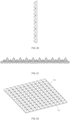
FIG. 1 is a three-dimensional schematic structural diagram of a diffuser according to an embodiment I of the present application from an angle; -
FIG. 2 is a three-dimensional schematic structural diagram of the diffuser according to the embodiment I of the present application from another angle; -
FIG. 3a to FIG. 3c are schematic arrangement diagrams of partial microlens structures on the diffuser according to the embodiment I of the present application; -
FIG. 4 is a schematic structural cross sectional view of the diffuser according to the embodiment I of the present application; -
FIG. 5a andFIG. 5b are arrangement effect diagrams of microlens structures of the diffuser according to the embodiment I of the present application; -
FIG. 6 is a structural cross sectional view of the diffuser according to the embodiment I of the present application when an error exists; -
FIG. 7 is an arrangement effect diagram of the microlens structures of the diffuser according to the embodiment I of the present application when an error exists; -
FIG. 8 is another arrangement effect diagram of the microlens structures of the diffuser according to the embodiment I of the present application when an error exists; -
FIG. 9 is a schematic arrangement diagram of filling patterns of the diffuser according to the embodiment I of the present application; -
FIG. 10 is a schematic diagram of filling the filling patterns of the diffuser according to the embodiment I of the present application with a reflective material; -
FIG. 11 is a schematic structural diagram of a filling pattern filled with the reflective material according to the embodiment I of the present application; -
FIG. 12 is a schematic position diagram of the filling patterns and lamp beads according to the embodiment I of the present application; -
FIG. 13 is a schematic structural diagram of a device configured to manufacture the diffuser according to the embodiment I of the present application; -
FIG. 14 is a schematic structural diagram of another device configured to manufacture the diffuser according to the embodiment I of the present application; -
FIG. 15 is a schematic structural diagram of layers of a backlight module according to the embodiment I of the present application; -
FIG. 16 is a schematic position diagram of the diffuser and the lamp bead in the backlight module according to the embodiment I of the present application; -
FIG. 17 is a schematic position diagram of the diffuser and the lamp bead in the backlight module according to an embodiment II of the present application; -
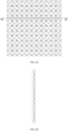
FIG. 18 is a three-dimensional schematic structural diagram of the diffuser when each convex lens is in the shape of a triangular pyramid according to an embodiment III of the present application; -
FIG. 19 is a schematic structural diagram of the diffuser inFIG. 18 from a top view; -
FIG. 20 is a schematic structural diagram of the diffuser inFIG. 18 from a side view; -
FIG. 21 is a cross sectional view of position A inFIG. 19 ; -
FIG. 22 is a three-dimensional schematic structural diagram of the diffuser when each convex lens is in the shape of a rectangular pyramid according to the embodiment III of the present application; -
FIG. 23 is a schematic structural diagram of the diffuser inFIG. 22 from a top view; -
FIG. 24 is a schematic structural diagram of the diffuser inFIG. 22 from a side view; and -
FIG. 25 is a cross sectional view of position B inFIG. 23 . - 1-Boss-shaped structure, 2-Recess-shaped structure, 3-Molten material, 4-Mold roller, 5-Base material layer, 6-Dispensing head, 7-Extrusion roller, 8-Mold roller, 9-Guide roller, 10-Ultraviolet light, 11-Lamp bead panel, 111-Lamp bead, 12-Diffuser, 121-Substrate, 122-Microlens structure, 1221-Recessed structure, 1222-Protrusion structure, 123-Filling pattern, 1231-Reflective material, 124-Convex lens, 13-Blue light film, 14-Quantum dot film, 15-First brightness enhancement film, 16-Second brightness enhancement film, 17-Diffusion film, 18-Light homogenizer.
- In order to further describe technical means adopted in the present invention to achieve the intended purposes of the present invention and effects thereof, specific implementations, structures, features, and effects of the present invention are described in detail below with reference to the drawings and preferred embodiments.
- A mini LED diffuser is provided according to an embodiment I of the prensent invention. The mini LED diffuser comprises a
substrate 121, a plurality ofmicrolens structures 122 located on one side of thesubstrate 121, and a filling structure located on the other side of thesubstrate 121. As shown inFIG. 1 and FIG. 2 , each of themicrolens structures 122 shown in the figure is a circular recessedstructure 1221. A recessed surface of themicrolens structure 122 is preferably a curved surface. The plurality ofmicrolens structures 122 are arranged in a plurality of rows. The plurality ofmicrolens structures 122 in two adjacent rows are arranged in a staggered manner, as shown inFIG. 3a , or arranged in a random manner, as shown inFIG. 3b , or arranged in an orthogonal manner, as shown inFIG. 3c . Twoadjacent microlens structures 122 partially overlap, as shown inFIG. 3a to FIG. 3c andFIG. 4 . A range of overlapping between twoadjacent microlens structures 122 is 5% to 25%, and preferably, is 10%. The design of partial overlapping between twoadjacent microlens structures 122 can not only effectively increase a coverage range of themicrolens structures 122 on the diffuser, so that a proportion of occupied space can reach 100%, as shown inFIG. 5a andFIG. 5b , but also overcome a positioning error of a laser head of a lithography machine. Current lithography machines on the market have a positioning precision in a range of 4 µm to 5 µm. During photolithography is performed on a lithographic piece, a positioning error may lead to a gap between patterned structures formed through the photolithography, thus forming a boss-shaped structure 1 and a recess-shapedstructure 2, as shown inFIG. 6 . During impression or extrusion to form themicrolens structure 122 on the diffuser, the structures may result in areas without themicrolens structure 122 on the diffuser, as shown inFIG. 7 andFIG. 8 . As a result, a diffusion effect of the diffuser is affected. - The diffusion effect of the diffuser relates to a radius of curvature and a size of the
microlens structure 122. Preferably, the size of themicrolens structure 122 is in a range of 0.03 mm to 0.09 mm, a depth is in a range of 0.01 mm to 0.05 mm, and the radius of curvature is in a range of 0.06 mm to 0.2 mm. It should be noted that the foregoing relevant parameter ranges of themicrolens structure 122 are a preferred range of the present application. During specific implementation, the relevant parameters of themicrolens structure 122 may be designed as required. - The filling structure comprises a plurality of structural units. The structural units comprise a plurality of filling
patterns 123 distributed based on equal density lines. The distribution density of the plurality of fillingpatterns 123 in one structural unit gradually decrease from a center of the one structural unit toward a periphery. As shown inFIG. 9 to FIG. 12 , the fillingpatterns 123 are distributed non-uniformly on the diffuser. Some areas have the fillingpatterns 123 distributed at a relatively large density, and some areas have the filling patterns distributed at a relatively small density. In each structural unit, the distribution density of the fillingpatterns 123 adjacent to a center (that is, adjacent to lamp beads 111) is greater than the distribution density of the fillingpatterns 123 away from the center (that is, away from the lamp beads 111). Each of the plurality of fillingpatterns 123 is a groove structure, and thefilling pattern 123 is filled with areflective material 1231, as shown inFIG. 10 . Preferably, the fillingpattern 123 is in the shape of a cylindrical counterbore, and a groove bottom of thefilling pattern 123 is in the shape of a circular arc. A sectional shape thereof is circular, square, or any other shape, and preferably, is circular. A size of the groove structure is in a range of 0.005 mm to 0.1 mm, and a depth of the groove structure is in a range of 0.004 mm to 0.05 mm. The fillingpattern 123 in the shape of the cylindrical counterbore can ensure that thereflective material 1231 can be perfectly filled into the fillingpattern 123 when thereflective material 1231 is scraped and coated, thereby effectively avoiding a failure in filling thereflective material 1231 or removal of the reflective material during the scraping and coating process. - The
reflective material 1231 is one of reflective ink, metallic silver, and metallic aluminum, but is not limited thereto. The reflective material may be another reflective material, or may be a mixture of a plurality of reflective materials. The reflective material is preferably reflective ink. Thereflective material 1231 is configured to reflect light. Light reflected by thereflective material 1231 can be reflected to the diffuser via alamp bead panel 11. In this way, light energy is fully utilized, and overall uniformity of light can be increased. It should be noted that thereflective material 1231 formed by a mixture of reflective ink with metallic silver or metallic aluminum is an existing material. During filling, volatile components such as water are added to thereflective material 1231. Therefore, during curing of thereflective material 1231, a middle position of thereflective material 1231 in each fillingpattern 123 is recessed inwardly by approximately 1 µm to 2 µm, forming a recessed surface on outside of thereflective material 1231, as shown inFIG. 11 . The recessed surface can effectively change a propagation direction of light emitted by thelamp beads 111, which improves a diffusion effect of the diffuser on the light emitted by thelamp beads 111. - Through the foregoing design of the varying density, high-intensity light adjacent to the
lamp beads 111 has a poor light transmission effect and a favorable light diffusion effect when passing through the fillingpatterns 123 with a relatively high aggregation coefficient, while low-intensity light away from thelamp beads 111 has a favorable light transmission effect and a poor light diffusion effect when passing through the fillingpatterns 123 with a relatively low aggregation coefficient. In this way, the diffuser has higher reflection efficiency at positions adjacent to thelamp beads 111 than positions away from thelamp beads 111, thereby achieving uniform light emission from a surface of the diffuser and eliminating non-uniform brightness of thelamp beads 111. It should be noted that in each structural unit on the diffuser, an area with fillingpatterns 123 distributed in a relatively large density corresponds to onelamp bead 111, and an area with fillingpatterns 123 distributed in a relatively small density corresponds to an area between twolamp beads 111, as shown inFIG. 12 . That is to say, a plurality of fillingpatterns 123 exist at a position on the diffuser corresponding to eachlamp bead 111, and the distribution density of the fillingpatterns 123 decreases with an increase of a distance from thelamp bead 111. - A thickness of the
substrate 121 of the diffuser is in a range of 0.1 mm to 2.0 mm. Athicker substrate 121 of the diffuser indicates a larger haze of the diffuser. Athinner substrate 121 indicates a higher transmittance of the diffuser. In the diffuser of the present application, two sides of thesubstrate 121 are respectively provided with themicrolens structures 122 and the filling structure, which can not only ensure the haze of the diffuser, but also improve the transmittance of the diffuser. For example, during manufacturing of a relatively thick diffuser (with a thickness greater than 0.6 mm), in order to ensure the haze of the diffuser, diffusion particles are added to a material for manufacturing the diffuser. However, the diffusion particles absorb light, which affects the transmittance of the diffuser. Themicrolens structures 122 of the present application can reduce a quantity of diffusion particles required to be added during manufacturing of the diffuser, and reduce absorption of light by the diffusion particles, which significantly improves the transmittance of the diffuser while ensuring the haze of the diffuser. It is learned through tests that the haze of the diffuser in the present application can reach 95%, and the transmittance can reach 85%, which is much higher than a transmittance of an existing diffuser in a range of 50% to 60%. The improvement in the transmittance can reduce a demand for a power for a mini LED. In this way, power consumption and to-be-dissipated heat are reduced, a service life of the mini LED is prolonged, and the mini LED is more environmentally friendly. - In this embodiment, a manufacturing process for the foregoing mini LED diffuser is further provided. Specific steps are as follows:
- Step S1: a plurality of first patterned structures corresponding to shapes of the
microlens structures 122 is formed on a side of a first lithographic piece, wherein adjacent first patterned structures partial overlap through photoetching; and a plurality of second patterned structures corresponding to the shapes of the fillingpatterns 123 on a side of a second lithographic piece through photoetching. The first lithographic piece and the second lithographic piece may be a glass substrate coated with photoresist on a single side. Afterwards, a photoresist layer is exposed according to a required pattern, and a developed part is etched to form a plurality of recessed patterned structures on the photoresist layer. The first lithographic piece and the second lithographic piece may also be made of specular metal materials. The metal materials may be stainless steel, nickel, copper, or the like. A high-power pulsed laser is directly caused to pass through an optical shaping path to focus on a surface of a metal base material for photolithography, thereby forming a desired patterned structure. - Step S2: the patterned structures on the obtained lithographic piece are transferred to a template by using an UV transfer printing technology or a metal growth technology, to obtain a template having the patterned structures. In this embodiment, the recessed first patterned structures on the first lithographic piece are transferred to a surface of the template through UV transfer, to obtain a first template having protruding patterned structures on the surface thereof. The recessed second patterned structures on the second lithographic piece are transferred to a surface of another template to obtain a second template having protruding patterned structures on a surface. Alternatively, the first template having the protruding patterned structures on the surface thereof and the second template having the protruding patterned structures on the surface thereof may be obtained through metal growth by electroforming. Certainly, the first template and the second template may be obtained in another manner.
- Step S3: the first template and the second template are wrapped on two
mold rollers 4 respectively, and a material for forming the diffuser is impressed or extruded, to obtain a semi-finished diffuser having themicrolens structures 122 and the filling structure on both sides thereof respectively. - Step S4: the filling structure is filled with a
reflective material 1231, and a finished diffuser is obtained by curing and molding. - In step S3, when a relatively thick diffuser needs to be manufactured, the diffuser is preferably integrally formed through extrusion, which requires an extrusion device. The extrusion device comprises two
mold rollers 4 for extrusion. The twomold rollers 4 are arranged parallelly and spaced apart from each other. An extrusion flow channel is formed between the two mold rollers. The first template and the second template are respectively wrapped around outside of the twomold rollers 4, and the patterned structures on the first template and the second template are oriented outward, as shown inFIG. 13 . The material for forming the diffuser comprises diffusion particles and a transparent organic polymer material. The transparent organic polymer material is any of PET, PC, and PMMA, but is not limited to these materials, which is not enumerated herein. The diffusion particles may be PET diffusion particles, PC diffusion particles, or PMMA diffusion particles. The diffusion particles are white diffusion particles or yellow diffusion particles, and preferably, are white diffusion particles, but are not limited to these diffusion particles. The diffusion particles may also be diffusion particles of another color. Specific manufacturing steps are as follows: - Step S311: the diffusion particles and the transparent organic polymer material are mixed and then melt to a molten state.
- Step S312: the melted
molten material 3 is added to an extrusion flow channel of the extrusion device for extrusion, and a distance between the twomold rollers 4 is adjusted to obtain a primary finished uniform diffuser with a corresponding thickness. - Step S313: a semi-finished diffuser having the
microlens structures 122 and the filling structure on the surfaces of the two sides respectively is obtained after cooling and curing. It should be noted that in this step, the cooling may be either natural cooling or cooling through cooling rollers, but is not limited to these manners, and may also be another cooling manner. - This embodiment further provides another manufacturing method, which is applicable to manufacturing of a relatively thin diffuser. It should be noted that, the diffuser herein may alternatively be referred to as a microlens diffusion film when a thickness thereof is relatively small. For ease of description, in the specification, the diffuser and the diffusion film are collectively referred to as a diffuser. A material for forming the diffuser in this method comprises a
base material layer 5 and a UV-cured resin. Thebase material layer 5 is any of PET, PC, and PMMA, but is not limited to these materials, which is not enumerated herein. As shown inFIG. 14 , specific manufacturing steps are as follows: - Step S321: the
base material layer 5 is provided. Thebase material layer 5 is any of PET, PC, and PMMA, but is not limited to these materials, which is not enumerated herein, or may be a diffusion material added with the diffusion particles. - Step S322: the UV-cured resin is coated on a surface of the base material. For example, the UV-cured resin is coated on a surface of the
base material layer 5 through a dispensinghead 6 shown inFIG. 14 , and then optionally, the UV-cured resin is cured by using an ultraviolet pre-curing device to form a semi-solid UV-cured resin layer on the surface of thebase material layer 5. The ultraviolet pre-curing device may be, for example, a low-power ultraviolet light, and can transform a UV-cured resin from an original liquid state into a semi-solid state for impression. - Step S323: UV impression is performed on the UV-cured resin layer by using a
mold roller 8 having the patterned structure on a surface. A manner of manufacturing themold roller 8 is the same as that in steps S1 to S3. During impression, the side of themold roller 8 with the patterned structure is caused to snugly contact the UV-cured resin through anextrusion roller 7, and then a patterned structure on the UV-cured resin is irradiated with anultraviolet light 10 so that the patterned structure is formed before being removed from themold roller 8. The patterned structure on the surface of themold roller 8 is transferred to the surface of thebase material layer 5. - Step S324: the
base material layer 5 is flipped by using aguide roller 9, the UV-cured resin is uniformly coated on a surface of the other side of thebase material layer 5, anothermold roller 8 is attached to the base material coated with the UV-cured resin, a UV-cured resin layer on the surface of thebase material layer 5 is cured, and a solid UV-cured resin layer on the surface of the other side of thebase material layer 5 is formed to obtain the semi-finished diffuser having themicrolens structures 122 and the filling structure on the surfaces of the two sides respectively. - Step S325: the filling structure is filled with the
reflective material 1231, and the finished diffuser is obtained by curing and molding. - In this manufacturing method, the two sides of the manufactured semi-finished diffuser are respectively provided with the
microlens structures 122 and the filling structure. Therefore, during impression, each single side may be impressed independently in sequence, or the two sides may be simultaneously impressed. Principles of the two impression manners are substantially the same, and therefore the details are not described herein. - It should be noted that in the foregoing two manufacturing methods, the mold roller may be manufactured by attaching a template with a required patterned structure on a surface thereof, or the required patterned structure may be directly manufactured on the surface of the mold roller. The template or the mold roller may be made of materials such as nickel, steel, copper, or aluminum.
- This embodiment further provides a backlight module, comprising the foregoing
mini LED diffuser 12. - The backlight module further comprises the
lamp bead panel 11, ablue light film 13, aquantum dot film 14, a firstbrightness enhancement film 15, a secondbrightness enhancement film 14, and adiffusion film 17 arranged in sequence, as shown inFIG. 15 . Thediffuser 12 is arranged between thelamp bead panel 11 and theblue light film 13. At least one layer ofdiffuser 12 is arranged. A side of thediffuser 12 filled with thereflective material 1231 faces thelamp bead panel 11, as shown inFIG. 16 . Each of the structural units on thediffuser 12 corresponds one of thelamp beads 111 on thelamp bead panel 11. In addition, one or more layers of light homogenizers may be added between theblue light film 13 and thediffusion film 17 or between the firstbrightness enhancement film 15 and thequantum dot film 14 as required. The light homogenizers may be provided with themicrolens structure 122 on both sides, or may be provided with themicrolens structures 122 on one side and a convex lens on the other side, as shown inFIG. 15 . - A difference between this embodiment II and the embodiment I is that the
microlens structures 122 on one side of the diffuser in this embodiment II is acircular protrusion structure 1222, as shown inFIG. 17 . A protruding surface of themicrolens structure 122 is preferably a curved surface. A manufacturing method for the diffuser and a backlight module structure using the diffuser in this embodiment are the same as those in the embodiment I, and therefore the details are not described herein. - A difference between this embodiment III and the embodiment I is that the microstructures on one side of the diffuser in this embodiment is
convex lenses 124. Eachconvex lens 124 is in the shape of one or more of a prism, a pyramid, a semi-cylinder, and a cone, or is in a composite shape composed of one or more of the shapes according to a set rule. When theconvex lens 124 is in the shape of the prism (such as a triangular prism) or the semi-cylinder, theconvex lenses 124 are arranged parallelly and sequentially on a side of thesubstrate 121, and an axis direction is parallel to the surface where the convex lenses are arranged. Bottom edges of two adjacentconvex lenses 124 intersect. When theconvex lens 124 is the shape of the pyramid, for example, a triangular pyramid shown inFIG. 18 to FIG. 21 , or a quadrangular pyramid shown inFIG. 22 to FIG. 25 , or the like, theconvex lenses 124 are arranged sequentially. The bottom edges of two adjacentconvex lenses 124 intersect, and the two bottom edges staggered each other coincide with a line of intersection, as shown inFIG. 19 orFIG. 23 . Certainly, theconvex lens 124 may alternatively be in the shape of another pyramid. This case is substantially the same, and therefore is not described in detail herein. When theconvex lens 124 is in the shape of the cone, bottoms of theconvex lenses 124 partially overlap. Similar to those of themicrolens structure 122, a coverage range of theconvex lenses 124 on the light homogenizer can be increased, and a proportion of occupied space can reach 100%. In addition, theconvex lens 124 may alternatively be in the shape of a crossed semi-cylinder formed by two semi-cylinders, such as an orthogonal cylinder. The convex lenses present a grid shape on a side of the light homogenizer. Certainly, the convex lens may alternatively be in a composite shape obtained by staggered two prism shapes or other shapes. A size of theconvex lens 124 is in a micrometer order. A height of theconvex lens 124 is preferably in a range of 0.01 mm to 0.1 mm. When theconvex lens 124 is in the shape of the cone, a cone angle thereof is preferably in a range of 60 degrees to 120 degrees. A preferred cone angle of a longitudinal section of the cone is 90 degrees. - A manufacturing method the diffuser for and a backlight module structure using the diffuser in this embodiment III are the same as those in the embodiment I, and therefore the details are not described herein.
- Terms such as "comprise", "include" or any other variants herein are intended to encompass non-exclusive inclusion. In addition to those elements listed, another element not explicitly listed may also be included.
- Directional words such as "front", "back", "up", and "down" herein are defined by positions of parts in the drawings and between the parts, and are merely used for clarity and convenience of description of the technical solutions. It should be understood that the use of the directional words should not limit the protection scope of the present application.
- The foregoing embodiments herein and features in the embodiments may be combined with each other in a case that no conflict occurs.
Claims (11)
- A mini LED diffuser, comprising a substrate, a plurality of microstructures disposed on one side of the substrate, and a filling structure disposed on an other side of the substrate,wherein the microstructures comprises a plurality of microlens structures and/or a plurality of convex lenses, the filling structure comprises a plurality of structural units, each structural unit comprises a plurality of filling patterns distributed based on equal density lines, and a distribution density of the filling patterns in one structural unit gradually decreases from a center of the one structural unit toward a periphery,wherein each of the filling patterns is a groove structure, and each of the filling patterns is filled with a reflective material.
- The mini LED diffuser according to claim 1, wherein each of the microlens structures comprises a recessed structure and/or a protrusion structure, the plurality of microlens structures are arranged in a plurality of rows, the plurality of microlens structures in two adjacent rows are arranged in an staggered, random, or orthogonal manner, two adjacent microlens structures partially overlap, a protruding surface of the protrusion structure is a curved surface, and a recessed surface of the recessed structure is a curved surface.
- The mini LED diffuser according to claim 2, wherein a size of each microlens structure is in a range of 0.03 mm to 0.09 mm, and a depth or a height of each microlens structure is in a range of 0.01 mm to 0.05 mm.
- The mini LED diffuser according to claim 1, wherein a thickness of the substrate is in a range of 0.1 mm to 2.0 mm, and a range of overlapping between two adjacent microlens structures is 5% to 25%.
- The mini LED diffuser according to claim 1, wherein each of the convex lenses is in a shape of one or more of a prism, a pyramid, a semi-cylinder, and a cone, or is in a composite shape composed of one or more of the prism, the pyramid, the semi-cylinder, and the cone according to a set rule; and a height of each convex lens is in a range of 0.01 mm to 0.1 mm, and when the convex lens is in the shape of the cone, a cone angle thereof is in a range of 60 degrees to 120 degrees.
- The mini LED diffuser according to claim 1, wherein each of the filling patterns is in a shape of a cylindrical counterbore, and a groove bottom of the filling pattern is in a shape of a circular arc;the reflective material is one or a combination of reflective ink, metallic silver, and metallic aluminum; anda size of each filling pattern is in a range of 0.005 mm to 0.1 mm, and a depth of each filling pattern is in a range of 0.004 mm to 0.05 mm.
- A manufacturing process for the mini LED diffuser according to claim 1, comprising:providing two mold rollers, wherein a plurality of first patterned structures corresponding to shapes of the microstructures are disposed on a surface of one of the mold rollers, adjacent first patterned structures partially overlap, and a plurality of second patterned structures corresponding to shapes of the filling patterns are disposed on a surface of the other of the mold rollers;impressing or extruding a material for forming the mini LED diffuser to obtain a semi-finished diffuser having the microstructures and the filling structure on both sides thereof respectively; andfilling the filling structure with a reflective material and obtaining the mini LED diffuser by curing and molding.
- The manufacturing process for the mini LED diffuser according to claim 7, wherein the material for forming the diffuser comprises diffusion particles and a transparent organic polymer material, and the manufacturing process further comprises:mixing the diffusion particles and the transparent organic polymer material and then melting same to a molten state;extruding the melted material through a flow channel formed between the two mold rollers;obtaining the semi-finished diffuser having the microstructures and the filling structure on both sides thereof respectively after cooling and curing; andfilling the filling structure with the reflective material and obtaining the mini LED diffuser by curing and molding.
- The manufacturing process for the mini LED diffuser according to claim 7, wherein the material for forming the diffuser comprises a base material layer and a UV-cured resin, and the manufacturing process further comprises:uniformly coating the UV-cured resin on a surface of the base material layer;attaching the mold rollers with the patterned structures to the base material layer coated with the UV-cured resin, curing a UV-cured resin layer on the surface of the base material layer, and forming a solid UV-cured resin layer on the surface of the base material layer, to obtain the semi-finished diffuser having the microstructures and the filling structure on both sides thereof respectively; andfilling the filling structure with the reflective material and obtaining the mini LED diffuser by curing and molding.
- A backlight module, comprising the mini LED diffuser according to claim 1.
- The backlight module according to claim 10, further comprising a lamp bead panel, a blue light film, a quantum dot film, a first brightness enhancement film, a second brightness enhancement film, and a diffusion film disposed in sequence, wherein the mini LED diffuser is disposed between the lamp bead panel and the blue light film, at least one layer of mini LED diffuser is disposed, one side of the mini LED diffuser filled with the reflective material faces the lamp bead panel, and each of the structural units on the mini LED diffuser corresponds one of lamp beads on the lamp bead panel.
Applications Claiming Priority (2)
| Application Number | Priority Date | Filing Date | Title |
|---|---|---|---|
| CN202110297612.1A CN113156558A (en) | 2021-03-19 | 2021-03-19 | Mini LED diffusion sheet, preparation process thereof and backlight module |
| PCT/CN2022/072542 WO2022193824A1 (en) | 2021-03-19 | 2022-01-18 | Mini led diffuser, preparation process therefor, and backlighting module |
Publications (2)
| Publication Number | Publication Date |
|---|---|
| EP4300179A1 true EP4300179A1 (en) | 2024-01-03 |
| EP4300179A4 EP4300179A4 (en) | 2024-09-11 |
Family
ID=76887987
Family Applications (1)
| Application Number | Title | Priority Date | Filing Date |
|---|---|---|---|
| EP22770184.4A Withdrawn EP4300179A4 (en) | 2021-03-19 | 2022-01-18 | MINI LED DIFFUSER, MANUFACTURING PROCESS AND BACKLIGHT MODULE |
Country Status (4)
| Country | Link |
|---|---|
| EP (1) | EP4300179A4 (en) |
| JP (1) | JP2024511071A (en) |
| CN (1) | CN113156558A (en) |
| WO (1) | WO2022193824A1 (en) |
Families Citing this family (7)
| Publication number | Priority date | Publication date | Assignee | Title |
|---|---|---|---|---|
| CN113156558A (en) * | 2021-03-19 | 2021-07-23 | 苏州维旺科技有限公司 | Mini LED diffusion sheet, preparation process thereof and backlight module |
| CN113721385B (en) * | 2021-08-18 | 2024-07-09 | 安徽芯瑞达科技股份有限公司 | Mini LED chip backlight module capable of uniformly emitting light |
| CN113721390B (en) * | 2021-09-02 | 2024-11-22 | 东莞市谷麦光学科技有限公司 | Diffusion film for mini LED backlight module and preparation method thereof, backlight module |
| CN114019727B (en) * | 2021-12-01 | 2025-01-07 | 广州森万象新材料科技有限公司 | A light-uniform film for backlight source packaging module and backlight source packaging module |
| CN114509894A (en) * | 2021-12-01 | 2022-05-17 | 广州森万象新材料科技有限公司 | Even light film and backlight source packaging module |
| CN118011514B (en) * | 2024-04-10 | 2024-07-05 | 成都理工大学 | A method and system for predicting the fluctuation and density of basin basement interface |
| CN119820764B (en) * | 2025-01-26 | 2026-05-05 | 盐城维盛新材料有限公司 | Design methods for roller dies, manufacturing methods for optical plates, and optical plates |
Family Cites Families (16)
| Publication number | Priority date | Publication date | Assignee | Title |
|---|---|---|---|---|
| JP2007256748A (en) * | 2006-03-24 | 2007-10-04 | Toppan Printing Co Ltd | Optical sheet and backlight unit for display and image display |
| CN101126821B (en) * | 2006-08-18 | 2011-06-08 | 鸿富锦精密工业(深圳)有限公司 | Optical board and the backlight module group using same |
| JP5066957B2 (en) * | 2007-03-14 | 2012-11-07 | 凸版印刷株式会社 | Optical sheet, backlight unit using the same, and display device |
| KR100918034B1 (en) * | 2007-10-31 | 2009-09-18 | 제일모직주식회사 | Diffusion plate comprising an optical sheet having a reflecting portion on the back and an optical sheet having a lenticular lens on the front |
| KR101576312B1 (en) * | 2007-12-21 | 2015-12-09 | 니폰 제온 가부시키가이샤 | Surface light source device |
| JP4518178B2 (en) * | 2008-04-15 | 2010-08-04 | ソニー株式会社 | Lens array sheet, optical member, light source, and liquid crystal display device |
| JP5428313B2 (en) * | 2008-12-08 | 2014-02-26 | 凸版印刷株式会社 | Light uniform element and backlight unit and display device using the same |
| JP2011048104A (en) * | 2009-08-26 | 2011-03-10 | Hitachi Maxell Ltd | Method for manufacturing optical adjusting member and optical adjusting member |
| TWI738824B (en) * | 2010-03-26 | 2021-09-11 | 友輝光電股份有限公司 | A method of forming an optical film |
| KR101265312B1 (en) * | 2011-03-15 | 2013-05-16 | 주식회사 엘지화학 | Micro-lens array sheet and backlight unit comprising the same |
| CN202209593U (en) * | 2011-09-08 | 2012-05-02 | 深圳市华星光电技术有限公司 | LED backlight module set and liquid crystal display device |
| CN202708984U (en) * | 2012-07-23 | 2013-01-30 | 冠捷显示科技(厦门)有限公司 | Diffusion plate of dot-matrix type diffusion structures and backlight module using same |
| KR20140047412A (en) * | 2012-10-12 | 2014-04-22 | 에스케이씨하스디스플레이필름(유) | Tandem array lens sheet |
| JP6826433B2 (en) * | 2016-12-28 | 2021-02-03 | デクセリアルズ株式会社 | Reflective diffuser, display device, projection device and lighting device |
| CN113156558A (en) * | 2021-03-19 | 2021-07-23 | 苏州维旺科技有限公司 | Mini LED diffusion sheet, preparation process thereof and backlight module |
| CN215728917U (en) * | 2021-03-19 | 2022-02-01 | 苏州维旺科技有限公司 | A Mini LED diffuser and backlight module |
-
2021
- 2021-03-19 CN CN202110297612.1A patent/CN113156558A/en active Pending
-
2022
- 2022-01-18 EP EP22770184.4A patent/EP4300179A4/en not_active Withdrawn
- 2022-01-18 WO PCT/CN2022/072542 patent/WO2022193824A1/en not_active Ceased
- 2022-01-18 JP JP2023557688A patent/JP2024511071A/en active Pending
Also Published As
| Publication number | Publication date |
|---|---|
| EP4300179A4 (en) | 2024-09-11 |
| WO2022193824A1 (en) | 2022-09-22 |
| CN113156558A (en) | 2021-07-23 |
| JP2024511071A (en) | 2024-03-12 |
Similar Documents
| Publication | Publication Date | Title |
|---|---|---|
| CN113156550A (en) | Mini LED light homogenizing sheet, preparation process thereof and backlight module | |
| KR102671598B1 (en) | optical device | |
| US7679828B2 (en) | Method and apparatus for aperture sculpting in a microlens array film | |
| WO2022193824A1 (en) | Mini led diffuser, preparation process therefor, and backlighting module | |
| US6480307B1 (en) | Plane light source unit and method for manufacturing holographic light-guide used for the same | |
| US6633351B2 (en) | Optical functionality sheet, and planar light source and image display apparatus using the same sheet | |
| US10578921B2 (en) | Brightness homogenizing member, backlight unit, and liquid crystal display device | |
| CN113009605A (en) | Mini LED micro-lens light-homogenizing sheet, preparation process thereof and backlight module | |
| EP2541290A2 (en) | Backlight device and liquid crystal display apparatus using the same | |
| CN215728917U (en) | A Mini LED diffuser and backlight module | |
| WO2023060799A1 (en) | Quantum dot light-homogenizing composite material and preparation process therefor | |
| US11862761B2 (en) | Light-emitting module and display apparatus | |
| CN215678833U (en) | A Mini LED microlens homogenizing sheet and backlight module | |
| CN215729185U (en) | Mini LED light homogenizing sheet and backlight module | |
| JP2013097876A (en) | Light diffusion member, light guide plate and surface light source device | |
| US20130286687A1 (en) | Light guide with a printed film | |
| KR101278347B1 (en) | A Optical Film Having Amorphous Pattern and a Method for Manufacturing the Same | |
| JP2012042610A (en) | Diffusion sheet, light source unit, and liquid crystal display device | |
| CN216387660U (en) | Quantum dot dodging composite material | |
| KR20050092450A (en) | Lenticular lens sheet, rear projection type screen, and rear projection type projector, and lenticular lens sheet producing method | |
| JP5648075B2 (en) | Method for manufacturing shape transfer resin sheet and resin sheet | |
| JP5310268B2 (en) | Optical sheet, backlight unit and display device | |
| JP2012074308A (en) | Light source unit and liquid crystal display device | |
| KR101906906B1 (en) | Mold frame for light guide plate, manufacturing method for light guide plate comprising the same and method for pattern forming using mold frame | |
| TWI836458B (en) | Light diffusion sheet, backlight unit, liquid crystal display device, information equipment, and manufacturing method of light diffusion sheet |
Legal Events
| Date | Code | Title | Description |
|---|---|---|---|
| STAA | Information on the status of an ep patent application or granted ep patent |
Free format text: STATUS: THE INTERNATIONAL PUBLICATION HAS BEEN MADE |
|
| PUAI | Public reference made under article 153(3) epc to a published international application that has entered the european phase |
Free format text: ORIGINAL CODE: 0009012 |
|
| STAA | Information on the status of an ep patent application or granted ep patent |
Free format text: STATUS: REQUEST FOR EXAMINATION WAS MADE |
|
| 17P | Request for examination filed |
Effective date: 20230927 |
|
| AK | Designated contracting states |
Kind code of ref document: A1 Designated state(s): AL AT BE BG CH CY CZ DE DK EE ES FI FR GB GR HR HU IE IS IT LI LT LU LV MC MK MT NL NO PL PT RO RS SE SI SK SM TR |
|
| DAV | Request for validation of the european patent (deleted) | ||
| DAX | Request for extension of the european patent (deleted) | ||
| A4 | Supplementary search report drawn up and despatched |
Effective date: 20240809 |
|
| RIC1 | Information provided on ipc code assigned before grant |
Ipc: G02B 5/02 20060101ALI20240806BHEP Ipc: G02F 1/1335 20060101AFI20240806BHEP |
|
| STAA | Information on the status of an ep patent application or granted ep patent |
Free format text: STATUS: THE APPLICATION HAS BEEN WITHDRAWN |
|
| 18W | Application withdrawn |
Effective date: 20241230 |