EP4297092A1 - Photodetectors with substrate extensions adjacent photodiodes and manufacturing method therefor - Google Patents
Photodetectors with substrate extensions adjacent photodiodes and manufacturing method therefor Download PDFInfo
- Publication number
- EP4297092A1 EP4297092A1 EP22205695.4A EP22205695A EP4297092A1 EP 4297092 A1 EP4297092 A1 EP 4297092A1 EP 22205695 A EP22205695 A EP 22205695A EP 4297092 A1 EP4297092 A1 EP 4297092A1
- Authority
- EP
- European Patent Office
- Prior art keywords
- substrate
- substrate extension
- photodiode
- top surface
- extension
- Prior art date
- Legal status (The legal status is an assumption and is not a legal conclusion. Google has not performed a legal analysis and makes no representation as to the accuracy of the status listed.)
- Pending
Links
Images




Classifications
-
- H—ELECTRICITY
- H10—SEMICONDUCTOR DEVICES; ELECTRIC SOLID-STATE DEVICES NOT OTHERWISE PROVIDED FOR
- H10F—INORGANIC SEMICONDUCTOR DEVICES SENSITIVE TO INFRARED RADIATION, LIGHT, ELECTROMAGNETIC RADIATION OF SHORTER WAVELENGTH OR CORPUSCULAR RADIATION
- H10F30/00—Individual radiation-sensitive semiconductor devices in which radiation controls the flow of current through the devices, e.g. photodetectors
- H10F30/20—Individual radiation-sensitive semiconductor devices in which radiation controls the flow of current through the devices, e.g. photodetectors the devices having potential barriers, e.g. phototransistors
- H10F30/21—Individual radiation-sensitive semiconductor devices in which radiation controls the flow of current through the devices, e.g. photodetectors the devices having potential barriers, e.g. phototransistors the devices being sensitive to infrared, visible or ultraviolet radiation
- H10F30/22—Individual radiation-sensitive semiconductor devices in which radiation controls the flow of current through the devices, e.g. photodetectors the devices having potential barriers, e.g. phototransistors the devices being sensitive to infrared, visible or ultraviolet radiation the devices having only one potential barrier, e.g. photodiodes
- H10F30/223—Individual radiation-sensitive semiconductor devices in which radiation controls the flow of current through the devices, e.g. photodetectors the devices having potential barriers, e.g. phototransistors the devices being sensitive to infrared, visible or ultraviolet radiation the devices having only one potential barrier, e.g. photodiodes the potential barrier being a PIN barrier
-
- H—ELECTRICITY
- H10—SEMICONDUCTOR DEVICES; ELECTRIC SOLID-STATE DEVICES NOT OTHERWISE PROVIDED FOR
- H10F—INORGANIC SEMICONDUCTOR DEVICES SENSITIVE TO INFRARED RADIATION, LIGHT, ELECTROMAGNETIC RADIATION OF SHORTER WAVELENGTH OR CORPUSCULAR RADIATION
- H10F39/00—Integrated devices, or assemblies of multiple devices, comprising at least one element covered by group H10F30/00, e.g. radiation detectors comprising photodiode arrays
- H10F39/80—Constructional details of image sensors
- H10F39/803—Pixels having integrated switching, control, storage or amplification elements
- H10F39/8033—Photosensitive area
-
- H—ELECTRICITY
- H10—SEMICONDUCTOR DEVICES; ELECTRIC SOLID-STATE DEVICES NOT OTHERWISE PROVIDED FOR
- H10F—INORGANIC SEMICONDUCTOR DEVICES SENSITIVE TO INFRARED RADIATION, LIGHT, ELECTROMAGNETIC RADIATION OF SHORTER WAVELENGTH OR CORPUSCULAR RADIATION
- H10F71/00—Manufacture or treatment of devices covered by this subclass
-
- H—ELECTRICITY
- H10—SEMICONDUCTOR DEVICES; ELECTRIC SOLID-STATE DEVICES NOT OTHERWISE PROVIDED FOR
- H10F—INORGANIC SEMICONDUCTOR DEVICES SENSITIVE TO INFRARED RADIATION, LIGHT, ELECTROMAGNETIC RADIATION OF SHORTER WAVELENGTH OR CORPUSCULAR RADIATION
- H10F71/00—Manufacture or treatment of devices covered by this subclass
- H10F71/121—The active layers comprising only Group IV materials
- H10F71/1212—The active layers comprising only Group IV materials consisting of germanium
-
- H—ELECTRICITY
- H10—SEMICONDUCTOR DEVICES; ELECTRIC SOLID-STATE DEVICES NOT OTHERWISE PROVIDED FOR
- H10F—INORGANIC SEMICONDUCTOR DEVICES SENSITIVE TO INFRARED RADIATION, LIGHT, ELECTROMAGNETIC RADIATION OF SHORTER WAVELENGTH OR CORPUSCULAR RADIATION
- H10F77/00—Constructional details of devices covered by this subclass
- H10F77/10—Semiconductor bodies
- H10F77/12—Active materials
- H10F77/122—Active materials comprising only Group IV materials
-
- H—ELECTRICITY
- H10—SEMICONDUCTOR DEVICES; ELECTRIC SOLID-STATE DEVICES NOT OTHERWISE PROVIDED FOR
- H10F—INORGANIC SEMICONDUCTOR DEVICES SENSITIVE TO INFRARED RADIATION, LIGHT, ELECTROMAGNETIC RADIATION OF SHORTER WAVELENGTH OR CORPUSCULAR RADIATION
- H10F77/00—Constructional details of devices covered by this subclass
- H10F77/10—Semiconductor bodies
- H10F77/14—Shape of semiconductor bodies; Shapes, relative sizes or dispositions of semiconductor regions within semiconductor bodies
- H10F77/147—Shapes of bodies
Definitions
- the present disclosure relates to photodetectors and more specifically to photodetectors with substrate extensions and adjacent photodiodes.
- Photodiodes can alter the electrical characteristics of photodiodes, and this allows photodiodes to convert optical signals into electrical signals. This is very useful for image sensors used in, for example, data communications devices.
- One issue that arises is that photodiodes that use silicon alone are generally limited to use within specific light wavelengths (e.g., between 190nm and 1100nm).
- impurities can be added to silicon or different materials can be used as alternatives to silicon.
- germanium germanium
- InGaAs indium gallium arsenide
- lead(II) sulfide PbS lead(II) sulfide
- Hg1-xCdxTe mercury cadmium telluride
- a substrate in structures herein includes a substrate base and a substrate extension.
- a photodiode contacts the substrate base.
- the substrate extension is adjacent the photodiode.
- An additional device contacts the substrate extension.
- a sidewall spacer is between the photodiode and the substrate extension.
- the additional device includes conductive elements within the substrate extension adjacent the sidewall spacer.
- Some methods herein form a photodetector material on a substrate base and pattern an opening through the photodetector material to expose the substrate base and to define a photodiode. Such methods form an insulator layer on sidewalls of the photodiode in the opening, grow a substrate extension from an exposed portion of the substrate base in the opening in processing that fills the opening with the substrate extension, and form an additional device on the substrate extension.
- Additional methods herein form a photodiode on a substrate base, form a sidewall spacer adjacent the photodiode, epitaxially form a substrate extension adjacent the photodiode, and form an additional device on the substrate extension.
- impurities (dopants) or non-silicon structures can be added to silicon-based photodiodes to broaden the light wavelengths at which the photodiodes will efficiently perform light to electrical signal conversion.
- An issue that arises is that, during manufacture, it can be difficult to form a defect-free non-silicon photo-absorption structure of a photodiode in a trench in a silicon substrate because the silicon substrate often readily combines with the non-silicon material, the trenches may not be formed properly, or the trenches may not fully fill with the non-silicon photo-absorption material, etc.
- forming a non-silicon material within trenches in a silicon substrate can result in the substrate and the non-silicon material within the trenches having a co-planar top surface. This results in the adjacent readout circuitry only being co-planar with the photo-absorption structure, which can limit design flexibility.
- structures herein are formed in processing that forms a full layer of the photo-absorption material on a substrate base, after which the photo-absorption material is patterned into the photodiode. Once such a patterned photodiode is in place on the substrate base, sidewall spacers are formed on the photodiode, and substrate extensions are grown from/on the substrate base between the non-silicon photodiode.
- the sidewall spacers keep the silicon extensions from combining with the non-silicon photodiode. Further, because trenches are not formed in the substrate, the processing herein avoids any issues with trench imperfections and/or trenches not completely or improperly being filled with the non-silicon photo-absorption material.
- the tops of the substrate extensions are not limited to being co-planar with the tops of the non-silicon photodiode. This permits the tops of the substrates extensions to be above or below the tops of the non-silicon photodiode, and also permits the tops of the substrates extensions to have planar regions and facets at locations where the substrate extensions meet the sidewall spacers. This gives designers much more flexibility when locating the readout circuitry and other components.
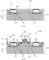
- FIG. 1 illustrates one such exemplary structure 100 that includes a substrate 101.
- the substrate 101 is made up of a substrate base 102 and epitaxially grown substrate extensions 104.
- the substrate extensions 104 are laterally adjacent and between the photodiodes 112 and such photodiodes 112 contact the substrate base 102.
- sidewall spacers 114, 116 are between the substrate extensions 104 and the photodiodes 112. Note that redundant number identification of repeated structures in the drawings is avoided to enhance drawing clarity and reduce clutter.
- the tops of the substrate extensions 104 are co-planar with the tops of the photodiodes 112 and sidewall spacers 114, 116. More specifically, each of the photodiodes 112 has a photodiode top surface 111.
- the substrate extensions 104 have substrate extension top surfaces 108 that lie in the same plane as the photodiode top surfaces 111.
- FIG. 1 shows that the substrate extensions 104 have a facet surface 106 between the sidewall spacers 116 and the substrate extension top surfaces 108, and the facet surface 106 is non-parallel to the planar substrate extension top surfaces 108.
- the sidewall spacers can include a first insulator layer 114 that contacts the photodiodes 112 and the substrate base 102.
- the first insulator layer 114 can have an "L" shape in cross-section.
- the sidewall spacers additionally include a second insulator layer 116 that contacts the first insulator layer 114 and the substrate extensions 104. In other words, the first insulator layer 114 separates, is between, and physically contacts the photodiode 112 and the second insulator 116.
- Additional devices 120 are on/in (and physically contact) the top surfaces 108 of the substrate extensions 104.
- the additional device 120 can be a field effect transistor 120, although any similar devices could be used as the additional devices 120.
- the additional device 120 shown can include a gate oxide 122 on (physically contacting) the substrate extension top surface 108, a gate conductor or gate conductor stack 128 on (physically contacting) the gate oxide 122, and source and drain regions (conductive elements/regions) 130, 132 within the substrate extensions 104 adjacent the sidewall spacers 116.
- a gate sidewall insulator 126 and sidewall spacer 124 are included with the additional device 120.
- FIG. 1 also illustrates that the structure 100 includes impurity regions 134 within the substrate 101 that electrically connect the photodiodes 112 to the source/drain region 130 of the additional devices 120.
- Further impurity regions 136 in the photodiode 112 complete the photodiode to form a PIN photodiode made of a P+ region, an Intrinsic layer, and an N+ region.
- the impurity regions 134, 136 can alternatively comprise the P+ and N+ regions, while the layer 112 can be the intrinsic (undoped) material, such as germanium, etc. While the intrinsic layer 112 and the impurity regions 134, 136 form the complete photodiode, for ease of reference such a PIN structure is often referred to herein simply as the "photodiode 112".
- a protective cap 118 is on (physically contacts) the photodiodes 112 (the cap 118 and the second insulator layer 116 can be the same material).
- the photodiodes 112, sidewall spacers 114, 116, and protective cap 118 form what is generically referred to as a photodetector structure 110.
- conductive contacts 140 are formed to the various elements including the substrate extensions 104, the photodiode structure 112, the gate conductor stack 128, the source/drain region 132, etc.
- the structure 200 shown in FIG. 2 is similar to the structure shown in FIG. 1 and the same components are identified using the same identification numbers.
- the structure 200 shown in FIG. 2 differs from the structure 100 shown in FIG. 1 by including substrate extensions 204 that have top surfaces 108 that are not co-planar with the top surfaces 108 of the photodiodes 112.
- the top surfaces 108 of the substrate extensions 204 are relatively closer to the substrate base 102 than are the top surfaces 108 of the photodiodes 112. This effectively raises the photodiodes 112 relative to the additional device 120 which can make processing that forms some of the contacts 140 easier and more accurate.
- the structure 300 shown in FIG. 3 is similar to the structure shown in FIG. 1 and the same components are identified using the same identification numbers.
- the structure 300 shown in FIG. 3 differs from the structure 100 shown in FIG. 1 by including substrate extensions 304 that have top surfaces 108 that are not co-planar with the top surfaces 108 of the photodiodes 112.
- the top surfaces 108 of the substrate extensions 304 are relatively further from the substrate base 102 than are the top surfaces 108 of the photodiodes 112. This effectively raises the additional device 120 relative to the photodiodes 112 which can make forming contacts to the additional device 120 easier and more accurate.
- the structure 300 shown in FIG. 3 includes an insulator layer 318 that is on (physically contacts) the substrate extensions 304, the photodetector structure 110, the additional device 120, etc.
- the insulator layer 318 can be formed of the same material as the sidewall spacers 124.
- FIG. 3 also shows that the structure includes a contact support 340 extending through the insulator layer 318 upon which the corresponding contact 142 is physically connected.
- a contact support 340 can be formed of a material (e.g., polysilicon, etc.) that more readily bonds with the material of the photodiode 112 and the (usually metal) material of the contacts 140, 142.
- FIG. 4 illustrates a structure 400 that is otherwise the same as the structure 300 shown in FIG. 3 but does not include the contact support 340. Instead, with the structure 400 shown in FIG. 4 , the corresponding contact 142 directly contacts the photodiodes 112 through the insulator layer 318.
- the structure 500 shown in FIG. 5 is similar to the structure shown in FIG. 1 and the same components are identified using the same identification numbers.
- the structure 500 shown in FIG. 5 differs from the structure 100 shown in FIG. 1 by including photodiodes 512 that have sidewalls that are not perpendicular to the top of the substrate base 102.
- the photodiodes 112 have sidewalls that are substantially perpendicular (e.g., within 5-10% of exactly perpendicular) to the top of the substrate base 102. This gives the photodiode 512 shown in FIG. 5 a trapezoid shape in cross-section.
- the sidewall spacers 114, 116 are similarly not perpendicular to the top of the substrate base 102.
- FIGs. 6-14 show some process steps that can be used to form the structure 100 shown in FIG. 1 .
- FIG. 6 illustrates processing that forms some of the impurity regions 134 and a layer of photo-absorption material 109 on the substrate base 102.
- the substrate base 102 can be any form of useful substrate, such as a bulk silicon substrate or a bulk semiconductor substrate of some other suitable semiconductor material.
- the impurity regions 134 are formed by implanting a sufficient concentration of dopants into the substrate base 102 before the photo-absorption material 109 is formed to have the impurity regions 134 create a conductive path through the substrate base 102.
- the photo-absorption material 109 can be grown or deposited on the substrate base 102 and can be, in some non-limiting examples, germanium (Ge), indium gallium arsenide (InGaAs), lead(II) sulfide PbS, mercury cadmium telluride (Hg1-xCdxTe), etc.
- implantation processes can take any appropriate form (whether now known or developed in the future) and can be, for example, ion implantation, etc.
- a semiconductor material refers to a material whose conducting properties can be altered by doping with an impurity.
- Exemplary semiconductor materials include, for example, silicon-based semiconductor materials (e.g., silicon, silicon germanium, silicon germanium carbide, silicon carbide, etc.) and III-V compound semiconductors (i.e., compounds obtained by combining group III elements, such as aluminum (Al), gallium (Ga), or indium (In), with group V elements, such as nitrogen (N), phosphorous (P), arsenic (As) or antimony (Sb)) (e.g., GaN, InP, GaAs, or GaP).
- group III elements such as aluminum (Al), gallium (Ga), or indium (In)
- group V elements such as nitrogen (N), phosphorous (P), arsenic (As) or antimony (Sb)
- group III elements such as aluminum (Al), gallium (Ga), or indium (In)
- group V elements such as nitrogen (N), phospho
- a pure semiconductor material and, more particularly, a semiconductor material that is not doped with an impurity for the purposes of increasing conductivity is referred to in the art as an intrinsic semiconductor.
- a semiconductor material that is doped with an impurity for the purposes of increasing conductivity is referred to in the art as an extrinsic semiconductor and will be more conductive than an intrinsic semiconductor made of the same base material. That is, extrinsic silicon will be more conductive than intrinsic silicon; extrinsic silicon germanium will be more conductive than intrinsic silicon germanium; and so on.
- semiconductor regions or layers are referred to as being either P-type semiconductor regions or layers or N-type semiconductor regions or layers. It should be understood that different impurities (i.e., different dopants) can be used to achieve different conductivity types (e.g., P-type conductivity and N-type conductivity) and that the dopants may vary depending upon the different semiconductor materials used.
- impurities i.e., different dopants
- conductivity types e.g., P-type conductivity and N-type conductivity
- the dopants may vary depending upon the different semiconductor materials used.
- a silicon-based semiconductor material e.g., silicon, silicon germanium, etc.
- a Group III dopant such as boron (B) or indium (In)
- P-type conductivity i.e., to form a P-type semiconductor region or layer
- a silicon-based semiconductor material is typically doped a Group V dopant, such as arsenic (As), phosphorous (P) or antimony (Sb), to achieve N-type conductivity (i.e., to form an N-type semiconductor region or layer).
- a Group III dopant such as boron (B) or indium (In
- Group V dopant such as arsenic (As), phosphorous (P) or antimony (Sb)
- a gallium nitride (GaN)-based semiconductor material is typically doped with magnesium (Mg) to achieve P-type conductivity (i.e., to form a P-type semiconductor region or layer) and with silicon (Si) or oxygen to achieve N-type conductivity (i.e., to form an N-type semiconductor region or layer).
- Mg magnesium
- Si silicon
- N-type conductivity i.e., to form an N-type semiconductor region or layer
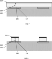
- a protective layer 118 (e.g., nitride, etc.) is formed on the photo-absorption material 109, as shown in FIG. 7 .
- a patterning process removes areas of the protective layer 118 and photo-absorption material 109 that are not protected by a mask, as shown in FIG. 8 . This leaves the photodiodes 112 on (vertically over or contacting) the impurity regions 134 because both are patterned in similar patterns.
- the terms vertical and horizontal may be used herein for convenience to refer to directions represented in the drawings; however, such terms are arbitrary and are only used as relative terms to indicate relatively perpendicular directions/orientations and such terms otherwise have no specific meaning and do not require that the structures itself be maintained in a specific orientation.
- the material to be patterned can be grown or deposited in any known manner and a patterning layer (such as an organic photoresist) can be formed over the material.
- the patterning layer (resist) can be exposed to some pattern of light radiation (e.g., patterned exposure, laser exposure, etc.) provided in a light exposure pattern, and then the resist is developed using a chemical agent. This process changes the physical characteristics of the portion of the resist that was exposed to the light. Then one portion of the resist can be rinsed off, leaving the other portion of the resist to protect the material to be patterned (which portion of the resist that is rinsed off depends upon whether the resist is a negative resist (illuminated portions remain) or positive resist (illuminated portions are rinsed off).
- a material removal process is then performed (e.g., wet etching, anisotropic etching (orientation dependent etching), plasma etching (reactive ion etching (RIE), etc.)) to remove the unprotected portions of the material below the resist to be patterned.
- the resist is subsequently removed to leave the underlying material patterned according to the light exposure pattern (or a negative image thereof).
- FIG. 9 illustrates the process of forming a first insulator layer 114 over the structure.
- the first insulator layer 114 can be any form of insulator, such as an oxide, etc. Oxides can be formed by heating a structure within an oxygen rich environment for a specific processing time.
- a second insulator layer 116 is formed over the structure.
- the first insulator layer 114 can be different from the second insulator layer 116 (which can be a nitride, etc.) because the first insulator layer 114 may be more compatible with the material of the photodiode 112, while the second insulator layer 116 may provide enhanced insulative, durability, and/or temperature characteristics.
- portions of the second insulator layer 116 are removed in sidewall spacer processing that can also remove the first insulator 114 from the protective layer 118 and from the top surface of the substrate base 102.
- sidewall spacers are generally formed by depositing or growing a conformal insulating layer and then performing a directional etching process (anisotropic) that etches material from horizontal surfaces at a greater rate than its removes material from vertical surfaces, thereby leaving insulating material along the vertical sidewalls of structures. This leaves what is referred to herein as the photodetector structures 110 over the impurity regions 134 in the substrate base 102.
- FIG. 12 illustrates that the substrate extensions 104 are formed on the areas of the substrate base 102 that are between the photodetector structures 110.
- the substrate extensions 104 can be formed by epitaxial growth processes. Epitaxial growth occurs in a heated (and sometimes pressurized) environment that is rich with a gas of the material that is to be grown. In such processing, a material that is similar or identical to the substrate base 102 can be epitaxially grown as the substrate extensions 104 (e.g., both can be a form of silicon).
- the substrate extensions 104 will show distinct crystalline structures that are unique to materials formed through epitaxial growth processes.
- facets 106 which can be curved surfaces or angled surfaces (that are non-parallel to the top 111 of the photodiode 112 and top 108 of the substrate extension 104)).
- the facets 106 are portions of the top surface 108 of the substrate extensions 104 in areas wherein the substrate extensions 104 contact the second insulator 116.
- Epitaxially growing the substrate extensions 104 provides design flexibility.
- FIG. 12 illustrates that the tops 108 of the substrate extensions 104 can be grown to be at the same vertical distance from the substrate base 102 as the tops 111 of the photodiodes (i.e., tops are in the same plane), as shown in FIGs. 2 and 3 above, controlling (lengthening or shortening) the epitaxial growth process can cause the tops 108 of the substrate extensions 104 to be farther or closer to the substrate base 102 relative to the tops 111 of the photodiodes 112 (i.e., tops are in different planes). Therefore, while FIGs. 6-14 illustrate formation of the structure 100 shown in FIG. 1 , one ordinarily skilled in the art would understand how to form the different height substrate extensions 204 and 304 shown in FIGs. 2-4 , that are discussed above, without specific illustration here.
- FIG. 13 illustrates that additional devices 120 are formed on the substrate extensions between each of the photodetector structures 110. While, in order to make the drawings clear, only a single additional device 120 illustrated, in the structures herein an additional device 120 can be positioned laterally adjacent each of photodetector structures 110 to allow the light signals detected by the photodetector structures 110 to be processed as digital data.
- any type of additional device 120 can be formed, depending upon the specific implementation.
- a standard field effect transistor (the varied formation processes of which are known and are evolving) is presented as one example of an additional device 120 and an exhaustive description of formation processes of field effect transistors is not germane to this disclosure.
- the formation processes of such additional devices 120 can include (among other steps): implantation of additional impurity regions 134 in the substrate extensions 104 and substrate base 102 to form a conductive path from the photodetector structure 110 to the additional device 120; formation of the gate oxide 122; formation of a non-functional gate structure; formation of gate sidewall structures 124, 126; implantation of impurities to form the source and drain regions 130, 132; replacement of the non-functional gate structure with a gate conductor 128; formation of overlying cap layers, etc.
- various conductive contacts 140 are formed to the photodetector structure 110, the gate conductor 128, one of the source or drain structures 132, etc.
- FIG. 14 is a substantial repeat of FIG. 1 and is represented to aid in reader comprehension.
- FIGs. 15-19 illustrate alternative processing resulting in alternative structures shown in FIG. 20 .
- FIG. 15 illustrates processing that provides the substrate base 102 (discussed above), forms the impurity regions 134 (discussed above), and forms the photo-absorptive material 109 (discussed above).
- FIG. 15 shows alternative processing where an insulator layer 171 (e.g., an oxide) is formed (e.g., grown in a heated oxide-rich environment) on the photo-absorptive material 109.
- an insulator layer 171 e.g., an oxide
- FIG. 16 using patterning processes similar to those described above, the photo-absorptive material 109 and insulator layer 171 are patterned. This again forms the photodiodes 112, as described above.
- FIG. 17 illustrates processing that forms an additional insulator 174 (again in a growth process) that may consume the insulator layer 171.
- FIG. 18 illustrates a patterning process that removes the additional insulator 174 from between the photodiodes 112.
- FIG. 19 uses the processing described above to epitaxially grow the substrate extensions 104 between the photodiodes 112. As noted above, the processing in FIG. 19 forms the facets 106 and the top 108 of the substrate extension 104 can be grown to different distances from the top of the substrate base 102 relative to the top 111 of the photodiode 112.
- FIG. 20 illustrates the same processing that is used to form the additional impurity regions 134 and the various components of the additional device 120 (e.g., source/drain 130, 132; sidewall spacers 124, 126; gate oxide 122; gate conductor 128; contacts 140; etc.).
- This results in structure 600 shown in FIG. 20 which is similar to the previous structures but uses a thinner sidewall spacer (single layer sidewall spacer 174) which can allow the structure to be more compact when compared to the other structures described herein.
- an "insulator” is a relative term that means a material or structure that allows substantially less ( ⁇ 95%) electrical current to flow than does a “conductor.”
- the dielectrics (insulators) mentioned herein can, for example, be grown from either a dry oxygen ambient or steam and then patterned.
- the dielectrics herein may be formed (grown or deposited) from any of the many candidate low dielectric constant materials (low-K (where K corresponds to the dielectric constant of silicon dioxide) materials such as fluorine or carbon-doped silicon dioxide, porous silicon dioxide, porous carbon-doped silicon dioxide, spin-on silicon or organic polymeric dielectrics, etc.) or high dielectric constant (high-K) materials, including but not limited to silicon nitride, silicon oxynitride, a gate dielectric stack of SiO 2 and Si 3 N 4 , hafnium oxide (HfO 2 ), hafnium zirconium oxide (HfZrO 2 ), zirconium dioxide (ZrO 2 ), hafnium silicon oxynitride (HfSiON), hafnium aluminum oxide compounds (HfAlO x ), other metal oxides like tantalum oxide, etc.
- the thickness of dielectrics herein may vary contingent upon the required device performance.
- the conductors mentioned herein can be formed of any conductive material, such as polycrystalline silicon (polysilicon), amorphous silicon, a combination of amorphous silicon and polysilicon, and polysilicon-germanium, rendered conductive by the presence of a suitable dopant.
- the conductors herein may be one or more metals, such as tungsten, hafnium, tantalum, molybdenum, titanium, or nickel, or a metal silicide, any alloys of such metals, and may be deposited using physical vapor deposition, chemical vapor deposition, or any other technique known in the art.
- a bipolar transistor has terminals labeled base, collector, and emitter. A small current at the base terminal (that is, flowing between the base and the emitter) can control, or switch, a much larger current between the collector and emitter terminals.
- a field-effect transistor which has terminals labeled gate, source, and drain. A voltage at the gate can control a current between source and drain.
- a semiconductor channel region is positioned between the conductive source region and the similarly conductive drain (or conductive source/emitter regions), and when the semiconductor is in a conductive state, the semiconductor allows electrical current to flow between the source and drain, or collector and emitter.
- the gate is a conductive element that is electrically separated from the semiconductor by a "gate oxide" (which is an insulator); and current/voltage within the gate changes makes the channel region conductive, allowing electrical current to flow between the source and drain. Similarly, current flowing between the base and the emitter makes the semiconductor conductive, allowing current to flow between the collector and emitter.
- a "gate oxide” which is an insulator
- laterally is used herein to describe the relative locations of elements and, more particularly, to indicate that an element is positioned to the side of another element as opposed to above or below the other element, as those elements are oriented and illustrated in the drawings.
- an element that is positioned laterally adjacent to another element will be beside the other element
- an element that is positioned laterally immediately adjacent to another element will be directly beside the other element
- an element that laterally surrounds another element will be adjacent to and border the outer sidewalls of the other element.
- Embodiments herein may be used in a variety of electronic applications, including but not limited to advanced sensors, memory/data storage, semiconductors, microprocessors and other applications.
- a resulting device and structure such as an integrated circuit (IC) chip can be distributed by the fabricator in raw wafer form (that is, as a single wafer that has multiple unpackaged chips), as a bare die, or in a packaged form. In the latter case the chip is mounted in a single chip package (such as a plastic carrier, with leads that are affixed to a motherboard or other higher level carrier) or in a multichip package (such as a ceramic carrier that has either or both surface interconnections or buried interconnections).
- a single chip package such as a plastic carrier, with leads that are affixed to a motherboard or other higher level carrier
- a multichip package such as a ceramic carrier that has either or both surface interconnections or buried interconnections.
- the chip is then integrated with other chips, discrete circuit elements, and/or other signal processing devices as part of either (a) an intermediate product, such as a motherboard, or (b) an end product.
- the end product can be any product that includes integrated circuit chips, ranging from toys and other low-end applications to advanced computer products having a display, a keyboard or other input device, and a central processor.
Landscapes
- Solid State Image Pick-Up Elements (AREA)
Abstract
A structure (100) comprising a substrate (101) comprising a substrate base (102) and a substrate extension (104) grown on the substrate base; a photodiode (112) contacting the substrate base, wherein the substrate extension is adjacent the photodiode; an additional device (120) contacting the substrate extension; and a sidewall spacer (114, 116) between the photodiode and the substrate extension, wherein the additional device includes conductive elements (130, 132) within the substrate extension adjacent the sidewall spacer.
Description
- The present disclosure relates to photodetectors and more specifically to photodetectors with substrate extensions and adjacent photodiodes.
- Light (photons) can alter the electrical characteristics of photodiodes, and this allows photodiodes to convert optical signals into electrical signals. This is very useful for image sensors used in, for example, data communications devices. One issue that arises is that photodiodes that use silicon alone are generally limited to use within specific light wavelengths (e.g., between 190nm and 1100nm).
- To expand photodiodes to additional wavelengths, impurities (dopants) can be added to silicon or different materials can be used as alternatives to silicon. For example, germanium (Ge), indium gallium arsenide (InGaAs), lead(II) sulfide PbS, mercury cadmium telluride (Hg1-xCdxTe), etc., can be used in place of, or with, silicon to expand the light wavelengths in which photodiodes operate with high light to electrical signal conversion efficiencies.
- In structures herein a substrate includes a substrate base and a substrate extension. In such structures, a photodiode contacts the substrate base. The substrate extension is adjacent the photodiode. An additional device contacts the substrate extension. A sidewall spacer is between the photodiode and the substrate extension. The additional device includes conductive elements within the substrate extension adjacent the sidewall spacer.
- Some methods herein form a photodetector material on a substrate base and pattern an opening through the photodetector material to expose the substrate base and to define a photodiode. Such methods form an insulator layer on sidewalls of the photodiode in the opening, grow a substrate extension from an exposed portion of the substrate base in the opening in processing that fills the opening with the substrate extension, and form an additional device on the substrate extension.
- Additional methods herein form a photodiode on a substrate base, form a sidewall spacer adjacent the photodiode, epitaxially form a substrate extension adjacent the photodiode, and form an additional device on the substrate extension.
- The embodiments herein will be better understood from the following detailed description with reference to the drawings, which are not necessarily drawn to scale and in which:
-
FIGs. 1-5 are cross-sectional conceptual diagrams illustrating photodiode structures according to embodiments herein; -
FIGs. 6-14 are cross-sectional conceptual diagrams illustrating processing steps for forming a photodiode structure according to embodiments herein; -
FIGs. 15-19 are cross-sectional conceptual diagrams illustrating processing steps for forming another photodiode structure according to embodiments herein; and -
FIG. 20 is a cross-sectional conceptual diagram illustrating a photodiode structure according to embodiments herein. - As mentioned above, impurities (dopants) or non-silicon structures can be added to silicon-based photodiodes to broaden the light wavelengths at which the photodiodes will efficiently perform light to electrical signal conversion. An issue that arises is that, during manufacture, it can be difficult to form a defect-free non-silicon photo-absorption structure of a photodiode in a trench in a silicon substrate because the silicon substrate often readily combines with the non-silicon material, the trenches may not be formed properly, or the trenches may not fully fill with the non-silicon photo-absorption material, etc.
- Additionally, forming a non-silicon material within trenches in a silicon substrate can result in the substrate and the non-silicon material within the trenches having a co-planar top surface. This results in the adjacent readout circuitry only being co-planar with the photo-absorption structure, which can limit design flexibility.
- In view of these and other issues, structures herein are formed in processing that forms a full layer of the photo-absorption material on a substrate base, after which the photo-absorption material is patterned into the photodiode. Once such a patterned photodiode is in place on the substrate base, sidewall spacers are formed on the photodiode, and substrate extensions are grown from/on the substrate base between the non-silicon photodiode.
- With these processes, defect-free photodiodes are consistently formed. Specifically, the sidewall spacers keep the silicon extensions from combining with the non-silicon photodiode. Further, because trenches are not formed in the substrate, the processing herein avoids any issues with trench imperfections and/or trenches not completely or improperly being filled with the non-silicon photo-absorption material.
- Additionally, with processing herein the tops of the substrate extensions are not limited to being co-planar with the tops of the non-silicon photodiode. This permits the tops of the substrates extensions to be above or below the tops of the non-silicon photodiode, and also permits the tops of the substrates extensions to have planar regions and facets at locations where the substrate extensions meet the sidewall spacers. This gives designers much more flexibility when locating the readout circuitry and other components.
-
FIG. 1 illustrates one suchexemplary structure 100 that includes asubstrate 101. As shown inFIG. 1 , thesubstrate 101 is made up of asubstrate base 102 and epitaxially grownsubstrate extensions 104. As shown, thesubstrate extensions 104 are laterally adjacent and between thephotodiodes 112 andsuch photodiodes 112 contact thesubstrate base 102. Additionally,sidewall spacers substrate extensions 104 and thephotodiodes 112. Note that redundant number identification of repeated structures in the drawings is avoided to enhance drawing clarity and reduce clutter. - Note that, in the
structure 100 shown inFIG. 1 , the tops of thesubstrate extensions 104 are co-planar with the tops of thephotodiodes 112 andsidewall spacers photodiodes 112 has a photodiodetop surface 111. Thesubstrate extensions 104 have substrateextension top surfaces 108 that lie in the same plane as thephotodiode top surfaces 111. Also,FIG. 1 shows that thesubstrate extensions 104 have afacet surface 106 between thesidewall spacers 116 and the substrateextension top surfaces 108, and thefacet surface 106 is non-parallel to the planar substrateextension top surfaces 108. - The sidewall spacers can include a
first insulator layer 114 that contacts thephotodiodes 112 and thesubstrate base 102. In one example, thefirst insulator layer 114 can have an "L" shape in cross-section. The sidewall spacers additionally include asecond insulator layer 116 that contacts thefirst insulator layer 114 and thesubstrate extensions 104. In other words, thefirst insulator layer 114 separates, is between, and physically contacts thephotodiode 112 and thesecond insulator 116. -
Additional devices 120 are on/in (and physically contact) thetop surfaces 108 of thesubstrate extensions 104. In the illustrated example, theadditional device 120 can be afield effect transistor 120, although any similar devices could be used as theadditional devices 120. Theadditional device 120 shown can include agate oxide 122 on (physically contacting) the substrateextension top surface 108, a gate conductor orgate conductor stack 128 on (physically contacting) thegate oxide 122, and source and drain regions (conductive elements/regions) 130, 132 within thesubstrate extensions 104 adjacent thesidewall spacers 116. Agate sidewall insulator 126 andsidewall spacer 124 are included with theadditional device 120. -
FIG. 1 also illustrates that thestructure 100 includesimpurity regions 134 within thesubstrate 101 that electrically connect thephotodiodes 112 to the source/drain region 130 of theadditional devices 120.Further impurity regions 136 in thephotodiode 112 complete the photodiode to form a PIN photodiode made of a P+ region, an Intrinsic layer, and an N+ region. For example, theimpurity regions layer 112 can be the intrinsic (undoped) material, such as germanium, etc. While theintrinsic layer 112 and theimpurity regions photodiode 112". - Additionally, a
protective cap 118 is on (physically contacts) the photodiodes 112 (thecap 118 and thesecond insulator layer 116 can be the same material). Thephotodiodes 112,sidewall spacers protective cap 118 form what is generically referred to as aphotodetector structure 110. Also,conductive contacts 140 are formed to the various elements including thesubstrate extensions 104, thephotodiode structure 112, thegate conductor stack 128, the source/drain region 132, etc. - The
structure 200 shown inFIG. 2 is similar to the structure shown inFIG. 1 and the same components are identified using the same identification numbers. Thestructure 200 shown inFIG. 2 differs from thestructure 100 shown inFIG. 1 by includingsubstrate extensions 204 that havetop surfaces 108 that are not co-planar with thetop surfaces 108 of thephotodiodes 112. Specifically, thetop surfaces 108 of thesubstrate extensions 204 are relatively closer to thesubstrate base 102 than are thetop surfaces 108 of thephotodiodes 112. This effectively raises thephotodiodes 112 relative to theadditional device 120 which can make processing that forms some of thecontacts 140 easier and more accurate. - The
structure 300 shown inFIG. 3 is similar to the structure shown inFIG. 1 and the same components are identified using the same identification numbers. Thestructure 300 shown inFIG. 3 differs from thestructure 100 shown inFIG. 1 by includingsubstrate extensions 304 that havetop surfaces 108 that are not co-planar with thetop surfaces 108 of thephotodiodes 112. Specifically, thetop surfaces 108 of thesubstrate extensions 304 are relatively further from thesubstrate base 102 than are thetop surfaces 108 of thephotodiodes 112. This effectively raises theadditional device 120 relative to thephotodiodes 112 which can make forming contacts to theadditional device 120 easier and more accurate. - Additionally, the
structure 300 shown inFIG. 3 includes aninsulator layer 318 that is on (physically contacts) thesubstrate extensions 304, thephotodetector structure 110, theadditional device 120, etc. Theinsulator layer 318 can be formed of the same material as thesidewall spacers 124. -
FIG. 3 also shows that the structure includes acontact support 340 extending through theinsulator layer 318 upon which thecorresponding contact 142 is physically connected. Such acontact support 340 can be formed of a material (e.g., polysilicon, etc.) that more readily bonds with the material of thephotodiode 112 and the (usually metal) material of thecontacts FIG. 4 illustrates astructure 400 that is otherwise the same as thestructure 300 shown inFIG. 3 but does not include thecontact support 340. Instead, with thestructure 400 shown inFIG. 4 , thecorresponding contact 142 directly contacts thephotodiodes 112 through theinsulator layer 318. - The
structure 500 shown inFIG. 5 is similar to the structure shown inFIG. 1 and the same components are identified using the same identification numbers. Thestructure 500 shown inFIG. 5 differs from thestructure 100 shown inFIG. 1 by includingphotodiodes 512 that have sidewalls that are not perpendicular to the top of thesubstrate base 102. In contrast, in thestructures photodiodes 112 have sidewalls that are substantially perpendicular (e.g., within 5-10% of exactly perpendicular) to the top of thesubstrate base 102. This gives thephotodiode 512 shown inFIG. 5 a trapezoid shape in cross-section. Further, thesidewall spacers substrate base 102. -
FIGs. 6-14 show some process steps that can be used to form thestructure 100 shown inFIG. 1 . Specifically,FIG. 6 illustrates processing that forms some of theimpurity regions 134 and a layer of photo-absorption material 109 on thesubstrate base 102. Specifically, thesubstrate base 102 can be any form of useful substrate, such as a bulk silicon substrate or a bulk semiconductor substrate of some other suitable semiconductor material. Theimpurity regions 134 are formed by implanting a sufficient concentration of dopants into thesubstrate base 102 before the photo-absorption material 109 is formed to have theimpurity regions 134 create a conductive path through thesubstrate base 102. As noted above, the photo-absorption material 109 can be grown or deposited on thesubstrate base 102 and can be, in some non-limiting examples, germanium (Ge), indium gallium arsenide (InGaAs), lead(II) sulfide PbS, mercury cadmium telluride (Hg1-xCdxTe), etc. As used herein, "implantation processes" can take any appropriate form (whether now known or developed in the future) and can be, for example, ion implantation, etc. - In the structures and method described herein, a semiconductor material refers to a material whose conducting properties can be altered by doping with an impurity. Exemplary semiconductor materials include, for example, silicon-based semiconductor materials (e.g., silicon, silicon germanium, silicon germanium carbide, silicon carbide, etc.) and III-V compound semiconductors (i.e., compounds obtained by combining group III elements, such as aluminum (Al), gallium (Ga), or indium (In), with group V elements, such as nitrogen (N), phosphorous (P), arsenic (As) or antimony (Sb)) (e.g., GaN, InP, GaAs, or GaP). A pure semiconductor material and, more particularly, a semiconductor material that is not doped with an impurity for the purposes of increasing conductivity (i.e., an undoped semiconductor material) is referred to in the art as an intrinsic semiconductor. A semiconductor material that is doped with an impurity for the purposes of increasing conductivity (i.e., a doped semiconductor material) is referred to in the art as an extrinsic semiconductor and will be more conductive than an intrinsic semiconductor made of the same base material. That is, extrinsic silicon will be more conductive than intrinsic silicon; extrinsic silicon germanium will be more conductive than intrinsic silicon germanium; and so on.
- Furthermore, semiconductor regions or layers are referred to as being either P-type semiconductor regions or layers or N-type semiconductor regions or layers. It should be understood that different impurities (i.e., different dopants) can be used to achieve different conductivity types (e.g., P-type conductivity and N-type conductivity) and that the dopants may vary depending upon the different semiconductor materials used. For example, a silicon-based semiconductor material (e.g., silicon, silicon germanium, etc.) is typically doped with a Group III dopant, such as boron (B) or indium (In), to achieve P-type conductivity (i.e., to form a P-type semiconductor region or layer), whereas a silicon-based semiconductor material is typically doped a Group V dopant, such as arsenic (As), phosphorous (P) or antimony (Sb), to achieve N-type conductivity (i.e., to form an N-type semiconductor region or layer). A gallium nitride (GaN)-based semiconductor material is typically doped with magnesium (Mg) to achieve P-type conductivity (i.e., to form a P-type semiconductor region or layer) and with silicon (Si) or oxygen to achieve N-type conductivity (i.e., to form an N-type semiconductor region or layer). Those skilled in the art will also recognize that different conductivity levels will depend upon the relative concentration levels of the dopant(s) in a given semiconductor region. Furthermore, when a semiconductor region or layer is described as being at a higher conductivity level than another semiconductor region or layer, it is more conductive (less resistive) than the other semiconductor region or layer; whereas, when a semiconductor region or layer is described as being at a lower conductivity level than another semiconductor region or layer, it is less conductive (more resistive) than that other semiconductor region or layer.
- A protective layer 118 (e.g., nitride, etc.) is formed on the photo-
absorption material 109, as shown inFIG. 7 . A patterning process removes areas of theprotective layer 118 and photo-absorption material 109 that are not protected by a mask, as shown inFIG. 8 . This leaves thephotodiodes 112 on (vertically over or contacting) theimpurity regions 134 because both are patterned in similar patterns. Note that the terms vertical and horizontal may be used herein for convenience to refer to directions represented in the drawings; however, such terms are arbitrary and are only used as relative terms to indicate relatively perpendicular directions/orientations and such terms otherwise have no specific meaning and do not require that the structures itself be maintained in a specific orientation. - When patterning any material herein, the material to be patterned can be grown or deposited in any known manner and a patterning layer (such as an organic photoresist) can be formed over the material. The patterning layer (resist) can be exposed to some pattern of light radiation (e.g., patterned exposure, laser exposure, etc.) provided in a light exposure pattern, and then the resist is developed using a chemical agent. This process changes the physical characteristics of the portion of the resist that was exposed to the light. Then one portion of the resist can be rinsed off, leaving the other portion of the resist to protect the material to be patterned (which portion of the resist that is rinsed off depends upon whether the resist is a negative resist (illuminated portions remain) or positive resist (illuminated portions are rinsed off). A material removal process is then performed (e.g., wet etching, anisotropic etching (orientation dependent etching), plasma etching (reactive ion etching (RIE), etc.)) to remove the unprotected portions of the material below the resist to be patterned. The resist is subsequently removed to leave the underlying material patterned according to the light exposure pattern (or a negative image thereof).
-
FIG. 9 illustrates the process of forming afirst insulator layer 114 over the structure. Thefirst insulator layer 114 can be any form of insulator, such as an oxide, etc. Oxides can be formed by heating a structure within an oxygen rich environment for a specific processing time. InFIG. 10 , asecond insulator layer 116 is formed over the structure. Thefirst insulator layer 114 can be different from the second insulator layer 116 (which can be a nitride, etc.) because thefirst insulator layer 114 may be more compatible with the material of thephotodiode 112, while thesecond insulator layer 116 may provide enhanced insulative, durability, and/or temperature characteristics. - As shown in
FIG. 11 , portions of thesecond insulator layer 116 are removed in sidewall spacer processing that can also remove thefirst insulator 114 from theprotective layer 118 and from the top surface of thesubstrate base 102. This leaves thefirst insulator layer 114 andsecond insulator layer 116 as sidewall spacers on the vertical sidewalls of thephotodiode 112. For purposes herein, sidewall spacers are generally formed by depositing or growing a conformal insulating layer and then performing a directional etching process (anisotropic) that etches material from horizontal surfaces at a greater rate than its removes material from vertical surfaces, thereby leaving insulating material along the vertical sidewalls of structures. This leaves what is referred to herein as thephotodetector structures 110 over theimpurity regions 134 in thesubstrate base 102. -
FIG. 12 illustrates that thesubstrate extensions 104 are formed on the areas of thesubstrate base 102 that are between thephotodetector structures 110. Specifically, thesubstrate extensions 104 can be formed by epitaxial growth processes. Epitaxial growth occurs in a heated (and sometimes pressurized) environment that is rich with a gas of the material that is to be grown. In such processing, a material that is similar or identical to thesubstrate base 102 can be epitaxially grown as the substrate extensions 104 (e.g., both can be a form of silicon). Thesubstrate extensions 104 will show distinct crystalline structures that are unique to materials formed through epitaxial growth processes. Further, this epitaxial growth process results in facets 106 (which can be curved surfaces or angled surfaces (that are non-parallel to the top 111 of thephotodiode 112 and top 108 of the substrate extension 104)). Thefacets 106 are portions of thetop surface 108 of thesubstrate extensions 104 in areas wherein thesubstrate extensions 104 contact thesecond insulator 116. - Epitaxially growing the
substrate extensions 104 provides design flexibility. Thus, whileFIG. 12 illustrates that thetops 108 of thesubstrate extensions 104 can be grown to be at the same vertical distance from thesubstrate base 102 as thetops 111 of the photodiodes (i.e., tops are in the same plane), as shown inFIGs. 2 and3 above, controlling (lengthening or shortening) the epitaxial growth process can cause thetops 108 of thesubstrate extensions 104 to be farther or closer to thesubstrate base 102 relative to thetops 111 of the photodiodes 112 (i.e., tops are in different planes). Therefore, whileFIGs. 6-14 illustrate formation of thestructure 100 shown inFIG. 1 , one ordinarily skilled in the art would understand how to form the differentheight substrate extensions FIGs. 2-4 , that are discussed above, without specific illustration here. -
FIG. 13 illustrates thatadditional devices 120 are formed on the substrate extensions between each of thephotodetector structures 110. While, in order to make the drawings clear, only a singleadditional device 120 illustrated, in the structures herein anadditional device 120 can be positioned laterally adjacent each ofphotodetector structures 110 to allow the light signals detected by thephotodetector structures 110 to be processed as digital data. - As noted above, any type of
additional device 120 can be formed, depending upon the specific implementation. Here a standard field effect transistor (the varied formation processes of which are known and are evolving) is presented as one example of anadditional device 120 and an exhaustive description of formation processes of field effect transistors is not germane to this disclosure. Briefly, the formation processes of suchadditional devices 120 can include (among other steps): implantation ofadditional impurity regions 134 in thesubstrate extensions 104 andsubstrate base 102 to form a conductive path from thephotodetector structure 110 to theadditional device 120; formation of thegate oxide 122; formation of a non-functional gate structure; formation ofgate sidewall structures regions gate conductor 128; formation of overlying cap layers, etc. - Following this, as shown in
FIG. 14 , various conductive contacts 140 (e.g., metals, alloys, polysilicon, etc.) are formed to thephotodetector structure 110, thegate conductor 128, one of the source or drainstructures 132, etc. Note thatFIG. 14 is a substantial repeat ofFIG. 1 and is represented to aid in reader comprehension. -
FIGs. 15-19 illustrate alternative processing resulting in alternative structures shown inFIG. 20 . Specifically,FIG. 15 illustrates processing that provides the substrate base 102 (discussed above), forms the impurity regions 134 (discussed above), and forms the photo-absorptive material 109 (discussed above).FIG. 15 shows alternative processing where an insulator layer 171 (e.g., an oxide) is formed (e.g., grown in a heated oxide-rich environment) on the photo-absorptive material 109. - As shown in
FIG. 16 , using patterning processes similar to those described above, the photo-absorptive material 109 andinsulator layer 171 are patterned. This again forms thephotodiodes 112, as described above.FIG. 17 illustrates processing that forms an additional insulator 174 (again in a growth process) that may consume theinsulator layer 171.FIG. 18 illustrates a patterning process that removes theadditional insulator 174 from between thephotodiodes 112. -
FIG. 19 uses the processing described above to epitaxially grow thesubstrate extensions 104 between thephotodiodes 112. As noted above, the processing inFIG. 19 forms thefacets 106 and the top 108 of thesubstrate extension 104 can be grown to different distances from the top of thesubstrate base 102 relative to the top 111 of thephotodiode 112. -
FIG. 20 illustrates the same processing that is used to form theadditional impurity regions 134 and the various components of the additional device 120 (e.g., source/drain sidewall spacers gate oxide 122;gate conductor 128;contacts 140; etc.). This results instructure 600 shown inFIG. 20 which is similar to the previous structures but uses a thinner sidewall spacer (single layer sidewall spacer 174) which can allow the structure to be more compact when compared to the other structures described herein. - For purposes herein, an "insulator" is a relative term that means a material or structure that allows substantially less (<95%) electrical current to flow than does a "conductor." The dielectrics (insulators) mentioned herein can, for example, be grown from either a dry oxygen ambient or steam and then patterned. Alternatively, the dielectrics herein may be formed (grown or deposited) from any of the many candidate low dielectric constant materials (low-K (where K corresponds to the dielectric constant of silicon dioxide) materials such as fluorine or carbon-doped silicon dioxide, porous silicon dioxide, porous carbon-doped silicon dioxide, spin-on silicon or organic polymeric dielectrics, etc.) or high dielectric constant (high-K) materials, including but not limited to silicon nitride, silicon oxynitride, a gate dielectric stack of SiO2 and Si3N4, hafnium oxide (HfO2), hafnium zirconium oxide (HfZrO2), zirconium dioxide (ZrO2), hafnium silicon oxynitride (HfSiON), hafnium aluminum oxide compounds (HfAlOx), other metal oxides like tantalum oxide, etc. The thickness of dielectrics herein may vary contingent upon the required device performance.
- The conductors mentioned herein can be formed of any conductive material, such as polycrystalline silicon (polysilicon), amorphous silicon, a combination of amorphous silicon and polysilicon, and polysilicon-germanium, rendered conductive by the presence of a suitable dopant. Alternatively, the conductors herein may be one or more metals, such as tungsten, hafnium, tantalum, molybdenum, titanium, or nickel, or a metal silicide, any alloys of such metals, and may be deposited using physical vapor deposition, chemical vapor deposition, or any other technique known in the art.
- There are various types of transistors, which have slight differences in how they are used in a circuit. For example, a bipolar transistor has terminals labeled base, collector, and emitter. A small current at the base terminal (that is, flowing between the base and the emitter) can control, or switch, a much larger current between the collector and emitter terminals. Another example is a field-effect transistor, which has terminals labeled gate, source, and drain. A voltage at the gate can control a current between source and drain. Within such transistors, a semiconductor (channel region) is positioned between the conductive source region and the similarly conductive drain (or conductive source/emitter regions), and when the semiconductor is in a conductive state, the semiconductor allows electrical current to flow between the source and drain, or collector and emitter. The gate is a conductive element that is electrically separated from the semiconductor by a "gate oxide" (which is an insulator); and current/voltage within the gate changes makes the channel region conductive, allowing electrical current to flow between the source and drain. Similarly, current flowing between the base and the emitter makes the semiconductor conductive, allowing current to flow between the collector and emitter.
- The terminology used herein is for the purpose of describing particular embodiments only and is not intended to be limiting of the foregoing. As used herein, the singular forms "a," "an," and "the" are intended to include the plural forms as well, unless the context clearly indicates otherwise. Furthermore, as used herein, terms such as "right", "left", "vertical", "horizontal", "top", "bottom", "upper", "lower", "under", "below", "underlying", "over", "overlying", "parallel", "perpendicular", etc., are intended to describe relative locations as they are oriented and illustrated in the drawings (unless otherwise indicated) and terms such as "touching", "in direct contact", "abutting", "directly adjacent to", "immediately adjacent to", etc., are intended to indicate that at least one element physically contacts another element (without other elements separating the described elements). The term "laterally" is used herein to describe the relative locations of elements and, more particularly, to indicate that an element is positioned to the side of another element as opposed to above or below the other element, as those elements are oriented and illustrated in the drawings. For example, an element that is positioned laterally adjacent to another element will be beside the other element, an element that is positioned laterally immediately adjacent to another element will be directly beside the other element, and an element that laterally surrounds another element will be adjacent to and border the outer sidewalls of the other element.
- Embodiments herein may be used in a variety of electronic applications, including but not limited to advanced sensors, memory/data storage, semiconductors, microprocessors and other applications. A resulting device and structure, such as an integrated circuit (IC) chip can be distributed by the fabricator in raw wafer form (that is, as a single wafer that has multiple unpackaged chips), as a bare die, or in a packaged form. In the latter case the chip is mounted in a single chip package (such as a plastic carrier, with leads that are affixed to a motherboard or other higher level carrier) or in a multichip package (such as a ceramic carrier that has either or both surface interconnections or buried interconnections). In any case the chip is then integrated with other chips, discrete circuit elements, and/or other signal processing devices as part of either (a) an intermediate product, such as a motherboard, or (b) an end product. The end product can be any product that includes integrated circuit chips, ranging from toys and other low-end applications to advanced computer products having a display, a keyboard or other input device, and a central processor.
- The elements herein can be modified to incorporate any number of variations, alterations, substitutions or equivalent arrangements not heretofore described, but which are commensurate with the spirit and scope herein. Additionally, while various embodiments have been described, it is to be understood that aspects herein may be included by only some of the described embodiments. Accordingly, the claims below are not to be seen as limited by the foregoing description. All structural and functional equivalents to the elements of the various embodiments described throughout this disclosure that are known or later, come to be known, to those of ordinary skill in the art are expressly incorporated herein by reference and intended to be encompassed by this disclosure. It is therefore to be understood that changes may be made in the particular embodiments disclosed which are within the scope of the foregoing as outlined by the appended claims.
- The following embodiments are explicitly disclosed:
- Embodiment 1:
A structure comprising:- a substrate comprising a substrate base and a substrate extension;
- a photodiode contacting the substrate base, wherein the substrate extension is adjacent the photodiode;
- an additional device contacting the substrate extension; and
- a sidewall spacer between the photodiode and the substrate extension,
- wherein the additional device includes conductive elements within the substrate extension adjacent the sidewall spacer.
- Embodiment 2:
- The structure according to embodiment 1, wherein the photodiode has a photodiode top surface, wherein the substrate extension has a substrate extension top surface that lies in a different plane from the photodiode top surface, and wherein
- the additional device contacts the substrate extension top surface.
- Embodiment 3:
The structure according to embodiment 1 or 2, wherein the substrate extension has a substrate extension top surface, wherein the substrate extension has a facet surface adjacent the sidewall spacer and the substrate extension top surface, and wherein the facet surface is non-parallel to the substrate extension top surface. - Embodiment 4:
The structure according to one of embodiments 1 to 3, wherein the sidewall spacer comprises:- a first insulator layer contacting the photodiode and the substrate base; and
- a second insulator layer contacting the first insulator layer and the substrate extension.
- Embodiment 5:
The structure according to embodiment 4, further comprising a cap contacting the photodiode, wherein the cap and the second insulator layer comprise the same material. - Embodiment 6:
The structure according to one of embodiments 1 to 5, wherein the substrate extension has a substrate extension top surface, wherein the additional device comprises a field effect transistor comprising: a gate oxide contacting the substrate extension top surface; and a gate conductor contacting the gate oxide, and wherein the conductive elements comprise source and drain regions of the field effect transistor. - Embodiment 7:
The structure according to one of embodiments 1 to 6, further comprising an impurity region within the substrate extension electrically connecting the photodiode to the additional device. - Embodiment 8:
A method comprising:- forming a photodetector material on a substrate base;
- patterning an opening through the photodetector material to expose the substrate base and to define a photodiode;
- forming an insulator layer on sidewalls of the photodiode in the opening;
- growing a substrate extension from an exposed portion of the substrate base in the opening in processing that fills the opening with the substrate extension; and
- forming an additional device on the substrate extension.
- Embodiment 9:
The method according to embodiment 8, wherein the growing of the substrate extension comprises an epitaxial growth process. - Embodiment 10:
The method according to embodiment 8 or 9, wherein the patterning of the opening forms the photodiode to have a photodiode top surface, wherein the growing of the substrate extension forms the substrate extension to have a substrate extension top surface that lies in a different plane from the photodiode top surface, and wherein the additional device is formed to contact the substrate extension top surface. - Embodiment 11:
The method according to one of embodiments 8 to 10, wherein the growing of the substrate extension forms the substrate extension to have a substrate extension top surface having a facet surface adjacent the photodiode and the substrate extension top surface, and wherein the facet surface is non-parallel to the substrate extension top surface. - Embodiment 12:
The method according to one of embodiments 8 to 11, further comprising forming an impurity region within the substrate extension electrically connecting the photodiode to the additional device. - Embodiment 13:
The method according to one of embodiments 8 to 12, further comprising forming a sidewall spacer layer on the insulator layer. - Embodiment 14:
The method according to one of embodiments 8 to 13, further comprising forming contacts to the photodetector material and the additional device. - Embodiment 15:
A method comprising:- forming a photodiode on a substrate base;
- forming sidewall spacer on the photodiode;
- epitaxially forming a substrate extension adjacent the photodiode; and
- forming an additional device on the substrate extension.
- Embodiment 16:
The method according to embodiment 15, wherein the photodiode is formed to have a photodiode top surface, wherein the substrate extension is formed to have a substrate extension top surface that lies in a different plane from the photodiode top surface, and wherein the additional device is formed to contact the substrate extension top surface. - Embodiment 17:
The method according to embodiment 15 or 16, wherein the substrate extension is formed to have a substrate extension top surface, wherein the substrate extension is formed to have a facet surface adjacent the sidewall spacer and the substrate extension top surface, and wherein the facet surface is formed to be non-parallel to the substrate extension top surface. - Embodiment 18:
The method according to one of embodiments 15 to 17, wherein the sidewall spacer is formed to comprise:- a first insulator layer contacting the photodiode and the substrate base; and
- a second insulator layer contacting the first insulator layer and the substrate extension.
- Embodiment 19:
The method according to embodiment 18, further comprising forming a cap on the photodiode, wherein the cap and the second insulator layer are formed of the same material. - Embodiment 20:
The method according to one of embodiments 15 to 19, wherein the substrate extension is formed to have a substrate extension top surface, wherein the additional device is formed as a field effect transistor comprising: a gate oxide contacting the substrate extension top surface; a gate conductor contacting the gate oxide; and source and drain regions.
Claims (15)
- A structure comprising:a substrate comprising a substrate base and a substrate extension;a photodiode contacting the substrate base, wherein the substrate extension is adjacent the photodiode;an additional device contacting the substrate extension; anda sidewall spacer between the photodiode and the substrate extension,wherein the additional device includes conductive elements within the substrate extension adjacent the sidewall spacer.
- The structure according to claim 1, wherein the photodiode has a photodiode top surface, wherein the substrate extension has a substrate extension top surface that lies in a different plane from the photodiode top surface, and wherein the additional device contacts the substrate extension top surface, and/or wherein the substrate extension has a substrate extension top surface, wherein the substrate extension has a facet surface adjacent the sidewall spacer and the substrate extension top surface, and wherein the facet surface is non-parallel to the substrate extension top surface, and/or wherein the substrate extension has a substrate extension top surface, wherein the additional device comprises a field effect transistor comprising: a gate oxide contacting the substrate extension top surface; and a gate conductor contacting the gate oxide, and wherein the conductive elements comprise source and drain regions of the field effect transistor, and/or wherein the structure further comprises an impurity region within the substrate extension electrically connecting the photodiode to the additional device..
- The structure according to claim 1 or 2, wherein the sidewall spacer comprises:a first insulator layer contacting the photodiode and the substrate base; anda second insulator layer contacting the first insulator layer and the substrate extension.
- The structure according to claim 3, further comprising a cap contacting the photodiode, wherein the cap and the second insulator layer comprise the same material.
- A method comprising:forming a photodiode on a substrate base;forming an insulator layer on the photodiode;forming a substrate extension adjacent the photodiode; andforming an additional device on the substrate extension.
- The method of claim 5, wherein forming the photodiode on the substrate base comprises:forming a photodetector material on the substrate base; andpatterning an opening through the photodetector material to expose the substrate base and to define a photodiode.
- The method of claim 5 or 6, wherein the insulator layer is formed on sidewalls of the photodiode in the opening.
- The method of one of claims 5 to 7, wherein forming the substrate extension comprises:
growing a substrate extension from an exposed portion of the substrate base in the opening in processing that fills the opening with the substrate extension, wherein the growing of the substrate extension preferably comprises an epitaxial growth process, and/or wherein the growing of the substrate extension preferably forms the substrate extension to have a substrate extension top surface having a facet surface adjacent the photodiode and the substrate extension top surface, the facet surface preferably being non-parallel to the substrate extension top surface. - The method according to claim 8 in combination with claim 6, wherein the patterning of the opening forms the photodiode to have a photodiode top surface, wherein the growing of the substrate extension forms the substrate extension to have a substrate extension top surface that lies in a different plane from the photodiode top surface, and wherein the additional device is formed to contact the substrate extension top surface.
- The method according to one of claims 5 to 9, further comprising forming an impurity region within the substrate extension electrically connecting the photodiode to the additional device, and/or forming a sidewall spacer layer on the insulator layer, and/or forming contacts to the photodetector material and the additional device.
- The method of one of claims 5 to 10, further comprising:forming a sidewall spacer on the photodiode, andwherein the substrate extension is epitaxially formed adjacent the photodiode.
- The method according to claim 11, wherein the photodiode is formed to have a photodiode top surface, wherein the substrate extension is formed to have a substrate extension top surface that lies in a different plane from the photodiode top surface, and wherein the additional device is formed to contact the substrate extension top surface.
- The method according to claim 11 or 12, wherein the substrate extension is formed to have a substrate extension top surface, wherein the substrate extension is formed to have a facet surface adjacent the sidewall spacer and the substrate extension top surface, and wherein the facet surface is formed to be non-parallel to the substrate extension top surface.
- The method according to one of claims 11 to 13, wherein the sidewall spacer is formed to comprise:a first insulator layer contacting the photodiode and the substrate base; anda second insulator layer contacting the first insulator layer and the substrate extension, wherein the method preferably further comprises forming a cap on the photodiode, the cap and the second insulator layer being formed of the same material.
- The method according to one of claims 11 to 14, wherein the substrate extension is formed to have a substrate extension top surface, wherein the additional device is formed as a field effect transistor comprising: a gate oxide contacting the substrate extension top surface; a gate conductor contacting the gate oxide; and source and drain regions.
Applications Claiming Priority (1)
| Application Number | Priority Date | Filing Date | Title |
|---|---|---|---|
| US17/807,887 US11777043B1 (en) | 2022-06-21 | 2022-06-21 | Photodetectors with substrate extensions adjacent photodiodes |
Publications (1)
| Publication Number | Publication Date |
|---|---|
| EP4297092A1 true EP4297092A1 (en) | 2023-12-27 |
Family
ID=84329513
Family Applications (1)
| Application Number | Title | Priority Date | Filing Date |
|---|---|---|---|
| EP22205695.4A Pending EP4297092A1 (en) | 2022-06-21 | 2022-11-07 | Photodetectors with substrate extensions adjacent photodiodes and manufacturing method therefor |
Country Status (2)
| Country | Link |
|---|---|
| US (1) | US11777043B1 (en) |
| EP (1) | EP4297092A1 (en) |
Cited By (1)
| Publication number | Priority date | Publication date | Assignee | Title |
|---|---|---|---|---|
| EP4383334A1 (en) * | 2022-12-06 | 2024-06-12 | GlobalFoundries U.S. Inc. | Photodiode with insulator layer along intrinsic region sidewall |
Citations (2)
| Publication number | Priority date | Publication date | Assignee | Title |
|---|---|---|---|---|
| US20160141329A1 (en) * | 2014-11-13 | 2016-05-19 | Artilux Inc. | Light absorption apparatus |
| EP3610510B1 (en) * | 2017-04-13 | 2021-07-14 | Artilux Inc. | Germanium-silicon light sensing apparatus |
Family Cites Families (7)
| Publication number | Priority date | Publication date | Assignee | Title |
|---|---|---|---|---|
| GB2247985A (en) | 1990-09-12 | 1992-03-18 | Philips Electronic Associated | Plural-wavelength infrared detector devices |
| US6465846B1 (en) * | 2000-03-22 | 2002-10-15 | Seiko Instruments Inc. | Semiconductor integrated circuit device having trench-type photodiode |
| US8257997B2 (en) * | 2007-10-17 | 2012-09-04 | Sifotonics Technologies (Usa) Inc. | Semiconductor photodetectors |
| US8558336B2 (en) | 2009-08-17 | 2013-10-15 | United Microelectronics Corp. | Semiconductor photodetector structure and the fabrication method thereof |
| US9348019B2 (en) | 2012-11-20 | 2016-05-24 | Visera Technologies Company Limited | Hybrid image-sensing apparatus having filters permitting incident light in infrared region to be passed to time-of-flight pixel |
| US10861888B2 (en) | 2015-08-04 | 2020-12-08 | Artilux, Inc. | Silicon germanium imager with photodiode in trench |
| TWI676282B (en) | 2015-08-04 | 2019-11-01 | 光澄科技股份有限公司 | Image sensor array |
-
2022
- 2022-06-21 US US17/807,887 patent/US11777043B1/en active Active
- 2022-11-07 EP EP22205695.4A patent/EP4297092A1/en active Pending
Patent Citations (2)
| Publication number | Priority date | Publication date | Assignee | Title |
|---|---|---|---|---|
| US20160141329A1 (en) * | 2014-11-13 | 2016-05-19 | Artilux Inc. | Light absorption apparatus |
| EP3610510B1 (en) * | 2017-04-13 | 2021-07-14 | Artilux Inc. | Germanium-silicon light sensing apparatus |
Cited By (2)
| Publication number | Priority date | Publication date | Assignee | Title |
|---|---|---|---|---|
| EP4383334A1 (en) * | 2022-12-06 | 2024-06-12 | GlobalFoundries U.S. Inc. | Photodiode with insulator layer along intrinsic region sidewall |
| US12349500B2 (en) | 2022-12-06 | 2025-07-01 | Globalfoundries U.S. Inc. | Photodiode with insulator layer along intrinsic region sidewall |
Also Published As
| Publication number | Publication date |
|---|---|
| US11777043B1 (en) | 2023-10-03 |
Similar Documents
| Publication | Publication Date | Title |
|---|---|---|
| US9806187B2 (en) | Method for manufacturing a semiconductor device | |
| US9478615B2 (en) | Blanket short channel roll-up implant with non-angled long channel compensating implant through patterned opening | |
| US10741451B2 (en) | FinFET having insulating layers between gate and source/drain contacts | |
| US10636894B2 (en) | Fin-type transistors with spacers on the gates | |
| US11777043B1 (en) | Photodetectors with substrate extensions adjacent photodiodes | |
| US7986022B2 (en) | Semispherical integrated circuit structures | |
| US8173524B1 (en) | Process for epitaxially growing epitaxial material regions | |
| US8816401B2 (en) | Heterojunction bipolar transistor | |
| US10297589B2 (en) | Electrostatic discharge and passive structures integrated in a vertical gate fin-type field effect diode | |
| US10964599B2 (en) | Multi-step insulator formation in trenches to avoid seams in insulators | |
| US20250338645A1 (en) | Structure with doped well between photodetector and optical interface of semiconductor layer | |
| US12557330B2 (en) | Semiconductor device including gate with different laterally adjacent sections and method | |
| US8957479B2 (en) | Formation of multi-height MUGFET | |
| US20230307539A1 (en) | Lateral diffusion field effect transistor with silicon-on-insulator region below field plate | |
| US20190319099A1 (en) | Vertical transistors having improved control of parasitic capacitance and source/drain-to-channel resistance | |
| US8647935B2 (en) | Buried oxidation for enhanced mobility | |
| US9202869B2 (en) | Self-aligned bipolar junction transistor having self-planarizing isolation raised base structures | |
| US11637181B2 (en) | Lateral bipolar transistors with polysilicon terminals | |
| US12356644B2 (en) | Gate tunnel current-triggered semiconductor controlled rectifier | |
| US20250194140A1 (en) | Multiple fin heights for effective width tuning | |
| US20240097029A1 (en) | Field effect transistor with adjustable effective gate length | |
| US20250287660A1 (en) | Backside merged source/drain contact | |
| US20190363174A1 (en) | Transistors having double spacers at tops of gate conductors | |
| US20130154003A1 (en) | Asymmetric anti-halo field effect transistor |
Legal Events
| Date | Code | Title | Description |
|---|---|---|---|
| PUAI | Public reference made under article 153(3) epc to a published international application that has entered the european phase |
Free format text: ORIGINAL CODE: 0009012 |
|
| STAA | Information on the status of an ep patent application or granted ep patent |
Free format text: STATUS: REQUEST FOR EXAMINATION WAS MADE |
|
| 17P | Request for examination filed |
Effective date: 20221107 |
|
| AK | Designated contracting states |
Kind code of ref document: A1 Designated state(s): AL AT BE BG CH CY CZ DE DK EE ES FI FR GB GR HR HU IE IS IT LI LT LU LV MC ME MK MT NL NO PL PT RO RS SE SI SK SM TR |