EP4297004A1 - Control circuit, control method and display apparatus - Google Patents
Control circuit, control method and display apparatus Download PDFInfo
- Publication number
- EP4297004A1 EP4297004A1 EP22930140.3A EP22930140A EP4297004A1 EP 4297004 A1 EP4297004 A1 EP 4297004A1 EP 22930140 A EP22930140 A EP 22930140A EP 4297004 A1 EP4297004 A1 EP 4297004A1
- Authority
- EP
- European Patent Office
- Prior art keywords
- feedback
- signal
- switching module
- power supply
- resistor
- Prior art date
- Legal status (The legal status is an assumption and is not a legal conclusion. Google has not performed a legal analysis and makes no representation as to the accuracy of the status listed.)
- Pending
Links
Images

Classifications
-
- G—PHYSICS
- G09—EDUCATION; CRYPTOGRAPHY; DISPLAY; ADVERTISING; SEALS
- G09G—ARRANGEMENTS OR CIRCUITS FOR CONTROL OF INDICATING DEVICES USING STATIC MEANS TO PRESENT VARIABLE INFORMATION
- G09G3/00—Control arrangements or circuits, of interest only in connection with visual indicators other than cathode-ray tubes
- G09G3/20—Control arrangements or circuits, of interest only in connection with visual indicators other than cathode-ray tubes for presentation of an assembly of a number of characters, e.g. a page, by composing the assembly by combination of individual elements arranged in a matrix no fixed position being assigned to or needed to be assigned to the individual characters or partial characters
- G09G3/34—Control arrangements or circuits, of interest only in connection with visual indicators other than cathode-ray tubes for presentation of an assembly of a number of characters, e.g. a page, by composing the assembly by combination of individual elements arranged in a matrix no fixed position being assigned to or needed to be assigned to the individual characters or partial characters by control of light from an independent source
- G09G3/3406—Control of illumination source
-
- G—PHYSICS
- G09—EDUCATION; CRYPTOGRAPHY; DISPLAY; ADVERTISING; SEALS
- G09G—ARRANGEMENTS OR CIRCUITS FOR CONTROL OF INDICATING DEVICES USING STATIC MEANS TO PRESENT VARIABLE INFORMATION
- G09G3/00—Control arrangements or circuits, of interest only in connection with visual indicators other than cathode-ray tubes
- G09G3/20—Control arrangements or circuits, of interest only in connection with visual indicators other than cathode-ray tubes for presentation of an assembly of a number of characters, e.g. a page, by composing the assembly by combination of individual elements arranged in a matrix no fixed position being assigned to or needed to be assigned to the individual characters or partial characters
- G09G3/34—Control arrangements or circuits, of interest only in connection with visual indicators other than cathode-ray tubes for presentation of an assembly of a number of characters, e.g. a page, by composing the assembly by combination of individual elements arranged in a matrix no fixed position being assigned to or needed to be assigned to the individual characters or partial characters by control of light from an independent source
- G09G3/36—Control arrangements or circuits, of interest only in connection with visual indicators other than cathode-ray tubes for presentation of an assembly of a number of characters, e.g. a page, by composing the assembly by combination of individual elements arranged in a matrix no fixed position being assigned to or needed to be assigned to the individual characters or partial characters by control of light from an independent source using liquid crystals
-
- G—PHYSICS
- G09—EDUCATION; CRYPTOGRAPHY; DISPLAY; ADVERTISING; SEALS
- G09G—ARRANGEMENTS OR CIRCUITS FOR CONTROL OF INDICATING DEVICES USING STATIC MEANS TO PRESENT VARIABLE INFORMATION
- G09G3/00—Control arrangements or circuits, of interest only in connection with visual indicators other than cathode-ray tubes
- G09G3/20—Control arrangements or circuits, of interest only in connection with visual indicators other than cathode-ray tubes for presentation of an assembly of a number of characters, e.g. a page, by composing the assembly by combination of individual elements arranged in a matrix no fixed position being assigned to or needed to be assigned to the individual characters or partial characters
- G09G3/34—Control arrangements or circuits, of interest only in connection with visual indicators other than cathode-ray tubes for presentation of an assembly of a number of characters, e.g. a page, by composing the assembly by combination of individual elements arranged in a matrix no fixed position being assigned to or needed to be assigned to the individual characters or partial characters by control of light from an independent source
- G09G3/3406—Control of illumination source
- G09G3/3413—Details of control of colour illumination sources
-
- H—ELECTRICITY
- H05—ELECTRIC TECHNIQUES NOT OTHERWISE PROVIDED FOR
- H05B—ELECTRIC HEATING; ELECTRIC LIGHT SOURCES NOT OTHERWISE PROVIDED FOR; CIRCUIT ARRANGEMENTS FOR ELECTRIC LIGHT SOURCES, IN GENERAL
- H05B45/00—Circuit arrangements for operating light-emitting diodes [LED]
- H05B45/50—Circuit arrangements for operating light-emitting diodes [LED] responsive to malfunctions or undesirable behaviour of LEDs; responsive to LED life; Protective circuits
- H05B45/59—Circuit arrangements for operating light-emitting diodes [LED] responsive to malfunctions or undesirable behaviour of LEDs; responsive to LED life; Protective circuits for reducing or suppressing flicker or glow effects
-
- G—PHYSICS
- G09—EDUCATION; CRYPTOGRAPHY; DISPLAY; ADVERTISING; SEALS
- G09G—ARRANGEMENTS OR CIRCUITS FOR CONTROL OF INDICATING DEVICES USING STATIC MEANS TO PRESENT VARIABLE INFORMATION
- G09G2310/00—Command of the display device
- G09G2310/02—Addressing, scanning or driving the display screen or processing steps related thereto
- G09G2310/0264—Details of driving circuits
- G09G2310/0291—Details of output amplifiers or buffers arranged for use in a driving circuit
-
- G—PHYSICS
- G09—EDUCATION; CRYPTOGRAPHY; DISPLAY; ADVERTISING; SEALS
- G09G—ARRANGEMENTS OR CIRCUITS FOR CONTROL OF INDICATING DEVICES USING STATIC MEANS TO PRESENT VARIABLE INFORMATION
- G09G2310/00—Command of the display device
- G09G2310/08—Details of timing specific for flat panels, other than clock recovery
-
- G—PHYSICS
- G09—EDUCATION; CRYPTOGRAPHY; DISPLAY; ADVERTISING; SEALS
- G09G—ARRANGEMENTS OR CIRCUITS FOR CONTROL OF INDICATING DEVICES USING STATIC MEANS TO PRESENT VARIABLE INFORMATION
- G09G2320/00—Control of display operating conditions
- G09G2320/02—Improving the quality of display appearance
- G09G2320/0247—Flicker reduction other than flicker reduction circuits used for single beam cathode-ray tubes
-
- G—PHYSICS
- G09—EDUCATION; CRYPTOGRAPHY; DISPLAY; ADVERTISING; SEALS
- G09G—ARRANGEMENTS OR CIRCUITS FOR CONTROL OF INDICATING DEVICES USING STATIC MEANS TO PRESENT VARIABLE INFORMATION
- G09G2320/00—Control of display operating conditions
- G09G2320/06—Adjustment of display parameters
- G09G2320/0626—Adjustment of display parameters for control of overall brightness
- G09G2320/064—Adjustment of display parameters for control of overall brightness by time modulation of the brightness of the illumination source
-
- G—PHYSICS
- G09—EDUCATION; CRYPTOGRAPHY; DISPLAY; ADVERTISING; SEALS
- G09G—ARRANGEMENTS OR CIRCUITS FOR CONTROL OF INDICATING DEVICES USING STATIC MEANS TO PRESENT VARIABLE INFORMATION
- G09G3/00—Control arrangements or circuits, of interest only in connection with visual indicators other than cathode-ray tubes
- G09G3/20—Control arrangements or circuits, of interest only in connection with visual indicators other than cathode-ray tubes for presentation of an assembly of a number of characters, e.g. a page, by composing the assembly by combination of individual elements arranged in a matrix no fixed position being assigned to or needed to be assigned to the individual characters or partial characters
- G09G3/22—Control arrangements or circuits, of interest only in connection with visual indicators other than cathode-ray tubes for presentation of an assembly of a number of characters, e.g. a page, by composing the assembly by combination of individual elements arranged in a matrix no fixed position being assigned to or needed to be assigned to the individual characters or partial characters using controlled light sources
- G09G3/30—Control arrangements or circuits, of interest only in connection with visual indicators other than cathode-ray tubes for presentation of an assembly of a number of characters, e.g. a page, by composing the assembly by combination of individual elements arranged in a matrix no fixed position being assigned to or needed to be assigned to the individual characters or partial characters using controlled light sources using electroluminescent panels
- G09G3/32—Control arrangements or circuits, of interest only in connection with visual indicators other than cathode-ray tubes for presentation of an assembly of a number of characters, e.g. a page, by composing the assembly by combination of individual elements arranged in a matrix no fixed position being assigned to or needed to be assigned to the individual characters or partial characters using controlled light sources using electroluminescent panels semiconductive, e.g. using light-emitting diodes [LED]
- G09G3/3208—Control arrangements or circuits, of interest only in connection with visual indicators other than cathode-ray tubes for presentation of an assembly of a number of characters, e.g. a page, by composing the assembly by combination of individual elements arranged in a matrix no fixed position being assigned to or needed to be assigned to the individual characters or partial characters using controlled light sources using electroluminescent panels semiconductive, e.g. using light-emitting diodes [LED] organic, e.g. using organic light-emitting diodes [OLED]
-
- H—ELECTRICITY
- H05—ELECTRIC TECHNIQUES NOT OTHERWISE PROVIDED FOR
- H05B—ELECTRIC HEATING; ELECTRIC LIGHT SOURCES NOT OTHERWISE PROVIDED FOR; CIRCUIT ARRANGEMENTS FOR ELECTRIC LIGHT SOURCES, IN GENERAL
- H05B45/00—Circuit arrangements for operating light-emitting diodes [LED]
- H05B45/10—Controlling the intensity of the light
- H05B45/14—Controlling the intensity of the light using electrical feedback from LEDs or from LED modules
-
- H—ELECTRICITY
- H05—ELECTRIC TECHNIQUES NOT OTHERWISE PROVIDED FOR
- H05B—ELECTRIC HEATING; ELECTRIC LIGHT SOURCES NOT OTHERWISE PROVIDED FOR; CIRCUIT ARRANGEMENTS FOR ELECTRIC LIGHT SOURCES, IN GENERAL
- H05B45/00—Circuit arrangements for operating light-emitting diodes [LED]
- H05B45/30—Driver circuits
- H05B45/32—Pulse-control circuits
- H05B45/325—Pulse-width modulation [PWM]
-
- Y—GENERAL TAGGING OF NEW TECHNOLOGICAL DEVELOPMENTS; GENERAL TAGGING OF CROSS-SECTIONAL TECHNOLOGIES SPANNING OVER SEVERAL SECTIONS OF THE IPC; TECHNICAL SUBJECTS COVERED BY FORMER USPC CROSS-REFERENCE ART COLLECTIONS [XRACs] AND DIGESTS
- Y02—TECHNOLOGIES OR APPLICATIONS FOR MITIGATION OR ADAPTATION AGAINST CLIMATE CHANGE
- Y02B—CLIMATE CHANGE MITIGATION TECHNOLOGIES RELATED TO BUILDINGS, e.g. HOUSING, HOUSE APPLIANCES OR RELATED END-USER APPLICATIONS
- Y02B20/00—Energy efficient lighting technologies, e.g. halogen lamps or gas discharge lamps
- Y02B20/30—Semiconductor lamps, e.g. solid state lamps [SSL] light emitting diodes [LED] or organic LED [OLED]
Definitions
- the present application relates to the technical field of display driving, and more particularly, to a control circuit, a control method, and a displaying device.
- a light-emitting diode In a back light of a display panel, a light-emitting diode is controlled to be turned on through PWM (Pulse Width Modulation).
- PWM Pulse Width Modulation
- an existing PWM signal is set as a low-level signal. In the case that a low-level PWM signal is converted into a current signal, the current value is low. The low current causes the amplitude of the voltage fluctuation at a feedback end of the light-emitting diode (LED) to become large. The large amplitude fluctuation of the voltage causes the fluctuation of the brightness of the light-emitting diode, resulting in continuous flickering of the light-emitting diode.
- LED light-emitting diode
- the present application provides a technical solution for reducing the continuous flickering of a light-emitting diode in the case of a low-level PWM signal.
- control circuit comprising:
- the present application further provides a control method, comprising:
- the present application further provides a displaying device, comprising a plurality of light emitting units and a control circuit as described above, wherein the feedback points are connected to the light emitting units in a one-to-one correspondence.
- the working power supply supplies power to the operation of the sampling module and the switching module, and the sampling module sends the collected level signal to the switching module,.
- the level signal corresponds to the pulse width modulation signal.
- the switching module is capable of being switched between the first mode and the second mode according to the driving level signal.
- the feedback points are mutually independent, and at this time, the current connected to each feedback point is also independent.
- the second mode the two feedback points are mutually associated, and at this time, the two feedback points are connected to the same line.
- the switching module is switched to the second mode, which is equivalent to merging the two low-current lines together, such that the magnitude of current in the line is increased.
- the brightness flicker of the LED is effectively reduced.
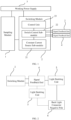
- the present application provides a control circuit, which includes a sampling module 1, a switching module 2, and a working power supply 3.
- the working power supply 3 is connected to the sampling module 1 and the switching module 2 and supplies power to the sampling module 1 and the switching module 2.
- the working power supply 3 is a direct-current power supply VCC, the power supply of the working power supply 3 ensures that various electronic components in the sampling module 1 and the switching module 2 operate and work normally, and the voltage of the working power supply 3 is 5 V or 12 V.
- the sampling module 1 is configured to collect a level signal corresponding to a pulse width modulation signal, which is also called a PWM signal for short.
- One end of the switching module 2 is connected to the sampling module 1, the other end of the switching module 2 is connected to at least one group of signal feedback ends 4, and each of the signal feedback ends 4 includes at least two feedback points.
- the number of the signal feedback ends 4 is multiple, and is not limited to one, for example, two or three, and the number of the feedback points in each group of the signal feedback ends 4 is not limited to two, and is three or more.
- the feedback points are configured to be connected to a light emitting unit 5.
- one end of the light emitting unit 5 is connected to the feedback point, and the other end of the light emitting unit 5 is connected to a positive pole 6 of a back light connector. By switching on the switching module 2, the light emitting unit 5 is turned on or off.
- the light emitting unit 5 is an LED (Light-Emitting Diode), an OLED (Organic Light-Emitting Diode), or an AMOLED (Active-Matrix Organic Light-Emitting Diode).
- the number of the light emitting units 5 connected to the feedback points is not limited to one, and a light string including a plurality of light emitting units 5 is provided.
- the switching module 2 is capable of be switched between a first mode and a second mode based on a relationship between the level signal and a preset threshold.
- the switching module 2 is capable of controlling mutual independence of the feedback points in the signal feedback ends 4, and the mutual independence of the feedback points means that the current or voltage between the feedback points is separated and each feedback point is provided with an independent circulating line.
- the switching module 2 is capable of controlling mutual association of the feedback points in the signal feedback ends 4, and the mutual association may be understood that the feedback points are connected together, and share one circulating line.
- the preset threshold is understood as a basis for judging a level of the level signal.
- the preset threshold is generally adjusted within the range of 0.1% to 10%, and the preset threshold is a specific value in the range or a range value. For example, in the case that the preset threshold is 5%, it is determined whether the switching module 2 is switched to the first mode or the second mode with 5% as a boundary.
- the preset threshold is also 0.1%, 0.3%, 0.5%, 1%, 2%, 3%, 4%, 6%, 7%, 8%, 9%, 10% and the like.
- the working power supply 3 supplies power to the operation of the sampling module 1 and the switching module 2, and the sampling module 1 sends the collected level signal to the switching module 2, where the level signal corresponds to the pulse width modulation signal.
- the switching module 2 is capable of being switched between the first mode and the second mode according to a driving level signal.
- the feedback points are mutually independent, and at this time, the current connected to each feedback point is also supplied independently through different lines.
- the two feedback points are mutually associated, and at this time, the two feedback points are connected to the same line.
- the switching module 2 is switched to the second mode, which is equivalent to merging the two low-current lines together, such that the magnitude of current in the line is increased.
- the switching module 2 is switched to the second mode, which is equivalent to merging the two low-current lines together, such that the magnitude of current in the line is increased.
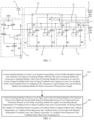
- the switching module 2 includes at least one group of constant current source sub-modules 21 and at least one group of switch controlling sub-modules 22, and the constant current source sub-modules 21, the switch controlling sub-modules 22, and the signal feedback ends 4 are disposed in one-to-one correspondence, where each of the switch controlling sub-modules 22 includes a first switch K1 and a second switch K2.
- Each of the constant current source sub-modules 21 includes at least two constant current sources, each of the constant current sources is provided with a power supply end, an input end, and an output end.
- the input end is connected to the sampling module 1 through an input line
- the power supply end is connected to the working power supply 3 through a power supply line
- the output end is connected to a feedback point of the signal feedback ends 4 through a feedback line.
- the constant current source provides a stable direct current
- the light emitting unit 5 keeps lighted through the stable direct current without disconnection at intervals. And thus there is no flickering stripes on a display screen, so that a picture is displayed well.
- the power supply end of the constant current source includes a positive pole of a power supply and a negative pole of the power supply, the positive pole of the power supply is connected to the working power supply 3, and the negative pole of the power supply is grounded.
- one power supply line is not provided with the first switch K1, and each of the remaining power supply lines is provided with the first switch K1.
- each feedback line connected to each feedback point is connected through the second switch; and one or more second switches K2 are provided.
- the plurality of second switches K2 communicate with the respective feedback lines.
- the working power supply 3 is always kept connected thereto. In this way, in the case that the first switches K1 in the remaining power supply lines are turned off, the second switches K2 are turned on, such that the constant current sources in the constant current source sub-modules 21 all communicate with the working power supply through one line.
- the first switches K1 are turned on, and the second switches K2 are turned off, and in the case that a plurality of first switches K1 and a plurality of second switches K2 are provided, the first switches K1 are all in an on state, and the second switches K2 are all in an off state.
- the first switches K1 are turned off, and the second switches K2 are turned on.
- the first switches K1 are all in an off state, and the second switches K2 are all in an on state.
- a plurality of constant current source sub-modules 21 are provided, the plurality of constant current source sub-modules 21 are disposed in parallel, and each constant current source sub-module 21 is connected to one group of signal feedback ends 4. It is seen that a plurality of signal feedback ends 4 are provided, a plurality of switch controlling sub-modules 22 are also provided, and each group of constant current sources is connected to one group of switch controlling sub-modules 22. Each group of switch controlling sub-modules 22 controls the connection state between each group of signal feedback ends 4 and the constant current source sub-modules 21. As shown in FIG. 3 , two constant current source sub-modules 21 are provided, but the number is not limited thereto, and more constant current source sub-modules 21 are provided.
- the switching module 2 further includes a control unit 23 connected to the switch controlling sub-modules 22, and the control unit 23 is configured to control the on or off of the first switches K1 and the on or off of the second switches K2.
- the control unit 23 is understood as an MCU (Microcontroller Unit), a memory is provided in the MCU, and the preset threshold is stored in the memory.
- the MCU further includes a processor.
- the processor is configured to call the preset threshold stored in the memory, to compare the duty ratio in the received PWM signal with the preset threshold in the memory, and to perform subsequent control operations according to the comparison result therebetween.
- the duty ratio of the PWM signal corresponds to the level signal collected by the sampling module 1, where the duty ratio is a ratio of a power-on time to a total time in one pulse signal cycle. It is known that the lower the duty ratio, the shorter the power-on time.
- the level signal collected by the sampling module 1 is converted from the duty ratio. In the case that the duty ratio is low, the level signal is at a low level, and in the case that the duty ratio is high, the level signal is at a high level.
- each of the constant current sources includes a first operational amplifier U1, a first field-effect transistor Q1, and a first resistor R1, a positive pole of a power supply of the first operational amplifier U1 is connected to the working power supply 3, a negative pole of the power supply of the first operational amplifier U1 is grounded, a signal input positive pole of the first operation amplifier U1 is connected to the sampling module 1, a signal input negative pole of the first operational amplifier U1 is connected to the first resistor R1, the other end of the first resistor R1 is grounded, a signal output end of the first operational amplifier U1 is connected to the first field-effect transistor Q1, one end of the first field-effect transistor Q1 is connected to the first resistor R1, and the other end of the first field-effect transistor Q1 is connected to one feedback point.
- one constant current source sub-module 21 includes two constant current sources, where one constant current source includes a first operational amplifier U1 and a first field-effect transistor Q1, and one end of the first operational amplifier U1 and one end of the first field-effect transistor Q1 are both connected to a first resistor R1; and the other constant current source includes a third operational amplifier U3 and a first field-effect transistor Q3, and one end of the third operational amplifier U3 and one end of the third field-effect transistor Q3 are both connected to a fourth resistor R4.
- the first switches K1 are turned on, and the second switches K2 are turned off, the two constant current sources are connected in parallel.
- the other constant current source sub-module 21 further includes two constant current sources, where one constant current source includes a fourth operational amplifier U4 and a fourth field-effect transistor Q4, and one end of the fourth operational amplifier U4 and one end of the fourth field-effect transistor Q4 are both connected to a fifth resistor R5; and the other constant current source includes a fifth operational amplifier U5 and a fifth field-effect transistor Q5, and one end of the fifth operational amplifier U5 and one end of the fifth field-effect transistor Q5 are both connected to a sixth resistor R6.
- the resistances of the first resistor R1, the fourth resistor R4, the fifth resistor R5, and the sixth resistor R6 are equal.
- the field-effect transistor is understood as an MOS transistor, which is the abbreviation of MOSFET.
- An MOSFE metal-oxide-semiconductor field-effect transistor is called MOSFET for short.
- MOSFET is a metal-oxide-semiconductor field-effect transistor, or a metal-insulator-semiconductor.
- G represents a gate
- S represents a source
- D represents a drain. The source and the drain of the MOS transistor are interchangeable.
- a sampling module 1 includes a second operational amplifier U2, a first sampling point A, and a second sampling point B, where the first sampling point A is connected to a signal input positive pole of the second operational amplifier U2, the second sampling point B is connected to a signal input negative pole of the second operational amplifier U2, and a second field-effect transistor Q2 is disposed between the signal input negative pole of the second operational amplifier U2 and the second sampling point B.
- the field-effect transistor is equivalent to a switch in the embodiment, and the second field-effect transistor Q2 is turned off at a low level and turned on at a high level. It is seen that the second field-effect transistor Q2 is turned off at the low level.
- the sampling module 1 further includes a second resistor R2 and a third resistor R3, where one end of the second field-effect transistor Q2 is connected to the second resistor R2, and the other end of the second resistor R2 is grounded; one end of the third resistor R3 is connected to the signal input negative pole of the second operational amplifier U2, the other end of the third resistor R3 is grounded, and a circuit formed by the second field-effect transistor Q2 and the second resistor R2 is connected in parallel with the third resistance R3.
- the second field-effect transistor Q2 is turned off, the current flows through the second resistor R2 and the third resistor R3, and in the case that the second resistor R2 is connected in series with the third resistor R3, as the resistance increases, the current flowing to the second operational amplifier U2 decreases.
- the second field-effect transistor Q2 is turned on, the current flows through the second field-effect transistor Q2, and at this time, in the case that the second resistor R2 is connected in parallel with the third resistor R3, as the resistance decreases, the current flowing to the second operational amplifier U2 increases.
- the signal input positive pole of the operational amplifier is understood as a positive phase input end, and the signal input negative pole of the operational amplifier is also understood as a negative phase input end.
- the sampling module 1 further includes a sixth field-effect transistor Q6 and a seventh field-effect transistor Q7, both of which are connected to the working power supply 3 and are connected in parallel.
- the other end of the sixth field-effect transistor Q6 and the other end of the seventh field-effect transistor Q7 are connected to an eighth field-effect transistor Q8.
- the eighth field-effect transistor Q8 is connected to an output end of the second operational amplifier U2.
- the first sampling point A and the second sampling point B are two lines extending from the same sampling point.
- the present application further provides a control method, which includes:
- a sampling module is controlled to collect a level signal corresponding to a pulse width modulation signal, and the level signal is transmitted to a switching module.
- One end of the switching module is connected to the sampling module, the other end of the switching module is connected to at least one group of signal feedback ends.
- Each of the signal feedback ends includes at least two feedback points, the feedback points are configured to be connected to a light emitting unit, and the switching module and the sampling module are both connected to a working power supply.
- the working power supply is a direct-current power supply, the power supply of the working power supply ensures that various electronic components in the sampling module and the switching module operate and work normally.
- the voltage of the working power supply is 5 V or 12 V.
- the sampling module is configured to collect a level signal corresponding to a pulse width modulation signal, which is also called a PWM signal for short.
- step S20 the switching module is controlled to receive the level signal, and the switching module is controlled be switched between a first mode and a second mode based on a relationship between the level signal and a preset threshold,
- the switching module In the first mode, the switching module is capable of controlling mutual independence of the feedback points in the signal feedback ends, and in the second mode, the switching module is capable of controlling mutual association of the feedback points in the signal feedback ends.
- the mutual association is understood that the feedback points are connected together, and share one circulating line.
- the preset threshold is understood as a basis for judging a level of the level signal.
- the preset threshold is generally adjusted within the range of 0.1% to 10%, and the preset threshold is a specific value in the range or a range value.
- the preset threshold is 5%
- the preset threshold is also 0.1%, 0.3%, 0.5%, 1%, 2%, 3%, 4%, 6%, 7%, 8%, 9%, 10% and the like.
- the step of controlling the switching module to be switched between the first mode and the second mode based on the relationship between the level signal and the preset threshold includes:
- a duty ratio representative of the level signal is acquired from a pulse width modulated signal,.
- the duty ratio is a ratio of a power-on time to a total time in one pulse signal cycle. It is known that the lower the duty ratio, the shorter the power-on time.
- the level signal collected by the sampling module is converted from the duty ratio. In the case that the duty ratio is low, the level signal is at a low level, and in the case that the duty ratio is high, the level signal is at a high level.
- step S220 the duty ratio is compared with a preset threshold, and a switching instruction is outputted according to the comparison result therebetween.
- step S230 in the case that the duty ratio is less than the preset threshold, a first switching instruction is output, and the switching module is controlled to be switched to the first mode according to the first switching instruction.
- the switching module In the first mode, the switching module is capable of controlling mutual independence of the feedback points in the signal feedback ends; and the mutual independence of the feedback points means that the current or voltage between the feedback points is separated and each feedback point is provided with an independent circulating line.
- step S240 in the case that the duty ratio is greater than or equal to the preset threshold, a second switching instruction is output, and the switching module is controlled to be switched to the second mode according to the second switching instruction.
- the switching module In the second mode, the switching module is capable of controlling mutual association of the feedback points in the signal feedback ends. The mutual association is understood that the feedback points are connected together, and share one circulating line.
- the feedback points are mutually independent, and in this case, the current connected to each feedback point is also independent.
- the two feedback points are mutually associated, and in this case, the two feedback points are connected to the same line.
- the switching module is switched to the second mode, which is equivalent to merging the two low-current lines together, such that the magnitude of current in the line is increased.
- the present application further provides a displaying device, which includes a plurality of light emitting units 5 and a control circuit, where the feedback points 41 are connected to the light emitting units 5 in a one-to-one correspondence.
- the switching module 2 in the control circuit controls the light emitting units 5 to be turned on.
- the displaying device includes, but is not limited to, a liquid crystal display panel, an organic light-emitting diode display panel, a field emission display panel, a plasma display panel and a curved panel.
- the liquid crystal panel includes a thin film transistor liquid crystal display panel, a TN (IN represents Twisted Nematic) panel, a VA (VA represents Wide Viewing Angle) panel, an IPS (IPS represents In-Plane Switching) panel, etc.
- the embodiments of the displaying device of the present application include all the technical solutions of all the embodiments of the above control circuit, and the technical effects achieved are completely the same, which will not be described here.
Landscapes
- Engineering & Computer Science (AREA)
- Physics & Mathematics (AREA)
- Computer Hardware Design (AREA)
- General Physics & Mathematics (AREA)
- Theoretical Computer Science (AREA)
- Chemical & Material Sciences (AREA)
- Crystallography & Structural Chemistry (AREA)
- Control Of Indicators Other Than Cathode Ray Tubes (AREA)
- Circuit Arrangement For Electric Light Sources In General (AREA)
- Dc-Dc Converters (AREA)
- Control Of El Displays (AREA)
Abstract
Description
- The present application claims priority to Chinese Patent Application No.
CN 202210498041.2, filed May 9, 2022 - The present application relates to the technical field of display driving, and more particularly, to a control circuit, a control method, and a displaying device.
- In a back light of a display panel, a light-emitting diode is controlled to be turned on through PWM (Pulse Width Modulation). However, an existing PWM signal is set as a low-level signal. In the case that a low-level PWM signal is converted into a current signal, the current value is low. The low current causes the amplitude of the voltage fluctuation at a feedback end of the light-emitting diode (LED) to become large. The large amplitude fluctuation of the voltage causes the fluctuation of the brightness of the light-emitting diode, resulting in continuous flickering of the light-emitting diode.
- The above information disclosed in this Background section is only for enhancement, primarily to reduce the understanding of the background of the present application, and therefore it may contain information that does not constitute the prior art that is already known to a person of ordinary skill in the art.
- The present application provides a technical solution for reducing the continuous flickering of a light-emitting diode in the case of a low-level PWM signal.
- According to a first aspect of the present application, the present application provides a control circuit, comprising:
- a sampling module configured to collect a level signal corresponding to a pulse width modulation signal;
- a switching module, wherein one end of the switching module is connected to the sampling module, the other end of the switching module is connected to at least one group of signal feedback ends, wherein each of the signal feedback ends comprises at least two feedback points, each of the feedback points is configured to be connected to a light emitting unit, and the switching module is capable of being switched between a first mode and a second mode based on a relationship between the level signal and a preset threshold; in the first mode, the switching module is capable of controlling mutual independence of the feedback points in the signal feedback ends; and in the second mode, the switching module is capable of controlling mutual association of the feedback points in the signal feedback ends, wherein the mutual independence of the feedback points represents that the feedback points are provided with mutually independent circulating lines, and the mutual association of the feedback points f represents that the feedback points share one circulating line; and
- a working power supply connected to the sampling module and the switching module and supplying power to the sampling module and the switching module.
- According to a second aspect of the present application, the present application further provides a control method, comprising:
- controlling a sampling module to collect a level signal corresponding to a pulse width modulation signal, and transmitting the level signal to a switching module, wherein one end of the switching module is connected to the sampling module, the other end of the switching module is connected to at least one group of signal feedback ends, wherein each of the signal feedback ends comprises at least two feedback points, each the feedback point is configured to be connected to a light emitting unit, and the switching module and the sampling module are both connected to a working power supply; and
- controlling the switching module to receive the level signal, and controlling the switching module to be switched between a first mode and a second mode based on a relationship between the level signal and a preset threshold, wherein in the first mode, the switching module is capable of controlling mutual independence of the feedback points in the signal feedback ends, and in the second mode, the switching module is capable of controlling mutual association of the feedback points in the signal feedback ends, wherein the mutual independence of the feedback points represents that the feedback points are provided with mutually independent circulating lines, and the mutual association of the feedback points represents that the feedback points share one circulating line.
- According to a third aspect of the present application, the present application further provides a displaying device, comprising a plurality of light emitting units and a control circuit as described above, wherein the feedback points are connected to the light emitting units in a one-to-one correspondence.
- In the technical solution of the present application, the working power supply supplies power to the operation of the sampling module and the switching module, and the sampling module sends the collected level signal to the switching module,. The level signal corresponds to the pulse width modulation signal. The switching module is capable of being switched between the first mode and the second mode according to the driving level signal. In the first mode, the feedback points are mutually independent, and at this time, the current connected to each feedback point is also independent. In the second mode, the two feedback points are mutually associated, and at this time, the two feedback points are connected to the same line. In the case of a low level signal, the switching module is switched to the second mode, which is equivalent to merging the two low-current lines together, such that the magnitude of current in the line is increased. Through the increase of current, the relative fluctuation of voltage is reduced, and the brightness of the LED tends to be stable without a change from high to low. Therefore, according to the technical solution, the brightness flicker of the LED is effectively reduced.
- It is to be understood that both the foregoing general description and the following detailed description are exemplary only, and are not intended to limit the present application.
- The accompanying drawings here, which are incorporated in and constitute a part of the specification, illustrate embodiments consistent with the present application and, together with the specification, serve to explain the principles of the present application.
- In order that the contents of the present disclosure may be more clearly understood, the present disclosure is described in further detail below in accordance with specific embodiments of the present disclosure and with reference to the accompanying drawings, in which:
-
FIG. 1 is a schematic diagram of a connection in a control circuit according to a first embodiment of the present application. -
FIG. 2 is a schematic diagram of a connection of a light emitting unit connected with the control circuit inFIG. 1 according to the present application. -
FIG. 3 is a circuit diagram according to the first embodiment of the present application. -
FIG. 4 is a flowchart of a control method according to a second embodiment of the present application. -
FIG. 5 is a detailed flowchart of step S20 according to the second embodiment of the present application. -
FIG. 6 is a schematic diagram of connections of light emitting units connected with the control circuit according to a third embodiment of the present application. - While the present application is susceptible of embodiments in many different forms, there is shown in the accompanying drawings and will be described in detail herein, only some of the embodiments, with the understanding that the specification is to be considered an exemplification of the principles of the present application and is not intended to limit the present application to that which is described herein.
- Thus, a feature indicated in the specification is intended to describe one of the features of one embodiment of the present application without implying that every embodiment of the present application must have the described feature. Furthermore, it should be noted that the specification describes a number of features. Although certain features may be combined together to illustrate a possible system design, these features may also be used in other combinations that are not explicitly described. Thus, the illustrated combinations are not intended to be limiting unless otherwise indicated.
- In the embodiments shown in the accompanying drawings, directional indications (such as up, down, left, right, front, and back) are used to explain that the structure and movement of the various elements of the present application are not absolute but relative. These descriptions are appropriate when the elements are in the positions shown in the accompanying drawings. If the description of the position of these elements changes, the indication of these directions changes accordingly.
- Example embodiments will now be described more fully with reference to the accompanying drawings. The example embodiments are capable, however, of being embodied in many forms and should not be construed as limited to the exemplars set forth herein; rather, they are provided so that the description of the present application will be thorough and complete, and will fully convey the concept of the example embodiments to those skilled in the art. The accompanying drawings are merely schematic illustrations of the present application and are not necessarily drawn to scale. The same reference numerals in the accompanying drawings denote the same or similar parts, and repeated description thereof will be omitted.
- The preferred embodiments of the present application are further described in detail below with reference to the accompanying drawings of the present specification.
- Referring to
FIG. 1 and FIG. 2 , the present application provides a control circuit, which includes asampling module 1, aswitching module 2, and aworking power supply 3. Theworking power supply 3 is connected to thesampling module 1 and theswitching module 2 and supplies power to thesampling module 1 and theswitching module 2. The workingpower supply 3 is a direct-current power supply VCC, the power supply of theworking power supply 3 ensures that various electronic components in thesampling module 1 and theswitching module 2 operate and work normally, and the voltage of theworking power supply 3 is 5 V or 12 V. Thesampling module 1 is configured to collect a level signal corresponding to a pulse width modulation signal, which is also called a PWM signal for short. One end of theswitching module 2 is connected to thesampling module 1, the other end of theswitching module 2 is connected to at least one group of signal feedback ends 4, and each of thesignal feedback ends 4 includes at least two feedback points. - It is noted that the number of the signal feedback ends 4 is multiple, and is not limited to one, for example, two or three, and the number of the feedback points in each group of the
signal feedback ends 4 is not limited to two, and is three or more. The feedback points are configured to be connected to alight emitting unit 5. In general, one end of thelight emitting unit 5 is connected to the feedback point, and the other end of thelight emitting unit 5 is connected to apositive pole 6 of a back light connector. By switching on theswitching module 2, thelight emitting unit 5 is turned on or off. Thelight emitting unit 5 is an LED (Light-Emitting Diode), an OLED (Organic Light-Emitting Diode), or an AMOLED (Active-Matrix Organic Light-Emitting Diode). - In addition, in the embodiment, the number of the
light emitting units 5 connected to the feedback points is not limited to one, and a light string including a plurality oflight emitting units 5 is provided. Theswitching module 2 is capable of be switched between a first mode and a second mode based on a relationship between the level signal and a preset threshold. In the first mode, theswitching module 2 is capable of controlling mutual independence of the feedback points in the signal feedback ends 4, and the mutual independence of the feedback points means that the current or voltage between the feedback points is separated and each feedback point is provided with an independent circulating line. In the second mode, theswitching module 2 is capable of controlling mutual association of the feedback points in the signal feedback ends 4, and the mutual association may be understood that the feedback points are connected together, and share one circulating line. The preset threshold is understood as a basis for judging a level of the level signal. The preset threshold is generally adjusted within the range of 0.1% to 10%, and the preset threshold is a specific value in the range or a range value. For example, in the case that the preset threshold is 5%, it is determined whether theswitching module 2 is switched to the first mode or the second mode with 5% as a boundary. In addition, the preset threshold is also 0.1%, 0.3%, 0.5%, 1%, 2%, 3%, 4%, 6%, 7%, 8%, 9%, 10% and the like. - In the technical solution of the embodiment, the working
power supply 3 supplies power to the operation of thesampling module 1 and theswitching module 2, and thesampling module 1 sends the collected level signal to theswitching module 2, where the level signal corresponds to the pulse width modulation signal. Theswitching module 2 is capable of being switched between the first mode and the second mode according to a driving level signal. In the first mode, the feedback points are mutually independent, and at this time, the current connected to each feedback point is also supplied independently through different lines. In the second mode, the two feedback points are mutually associated, and at this time, the two feedback points are connected to the same line. In the case of a low level signal, theswitching module 2 is switched to the second mode, which is equivalent to merging the two low-current lines together, such that the magnitude of current in the line is increased. Through the increase of current, the relative fluctuation of voltage is reduced, and the brightness of the LED tends to be stable without a change from high to low. Therefore, according to the technical solution, the brightness flicker of the LED is effectively reduced. - Referring to
FIG. 3 , in order to effectively complete the switching operation of theswitching module 2, theswitching module 2 includes at least one group of constant current source sub-modules 21 and at least one group ofswitch controlling sub-modules 22, and the constant current source sub-modules 21, theswitch controlling sub-modules 22, and the signal feedback ends 4 are disposed in one-to-one correspondence, where each of theswitch controlling sub-modules 22 includes a first switch K1 and a second switch K2. - Each of the constant current source sub-modules 21 includes at least two constant current sources, each of the constant current sources is provided with a power supply end, an input end, and an output end. The input end is connected to the
sampling module 1 through an input line, the power supply end is connected to the workingpower supply 3 through a power supply line, and the output end is connected to a feedback point of the signal feedback ends 4 through a feedback line. The constant current source provides a stable direct current, and thelight emitting unit 5 keeps lighted through the stable direct current without disconnection at intervals. And thus there is no flickering stripes on a display screen, so that a picture is displayed well. The power supply end of the constant current source includes a positive pole of a power supply and a negative pole of the power supply, the positive pole of the power supply is connected to the workingpower supply 3, and the negative pole of the power supply is grounded. - Among the plurality of power supply lines, one power supply line is not provided with the first switch K1, and each of the remaining power supply lines is provided with the first switch K1. Among the
signal feedback end 4, each feedback line connected to each feedback point is connected through the second switch; and one or more second switches K2 are provided. In the case that a plurality of second switches K2 are provided, the plurality of second switches K2 communicate with the respective feedback lines. In the constant current source connected to the power supply line not provided with the first switch K1, the workingpower supply 3 is always kept connected thereto. In this way, in the case that the first switches K1 in the remaining power supply lines are turned off, the second switches K2 are turned on, such that the constant current sources in the constant current source sub-modules 21 all communicate with the working power supply through one line. - Specifically, during the operation of the
switching module 2, in the first mode, the first switches K1 are turned on, and the second switches K2 are turned off, and in the case that a plurality of first switches K1 and a plurality of second switches K2 are provided, the first switches K1 are all in an on state, and the second switches K2 are all in an off state. In the second mode, the first switches K1 are turned off, and the second switches K2 are turned on. Similarly, in the case that a plurality of first switches K1 and a plurality of second switches K2 are provided, the first switches K1 are all in an off state, and the second switches K2 are all in an on state. - In one of aspects, a plurality of constant current source sub-modules 21 are provided, the plurality of constant current source sub-modules 21 are disposed in parallel, and each constant current source sub-module 21 is connected to one group of signal feedback ends 4. It is seen that a plurality of signal feedback ends 4 are provided, a plurality of
switch controlling sub-modules 22 are also provided, and each group of constant current sources is connected to one group ofswitch controlling sub-modules 22. Each group ofswitch controlling sub-modules 22 controls the connection state between each group of signal feedback ends 4 and the constant current source sub-modules 21. As shown inFIG. 3 , two constant current source sub-modules 21 are provided, but the number is not limited thereto, and more constant current source sub-modules 21 are provided. - In one of aspects, the
switching module 2 further includes acontrol unit 23 connected to theswitch controlling sub-modules 22, and thecontrol unit 23 is configured to control the on or off of the first switches K1 and the on or off of the second switches K2. Thecontrol unit 23 is understood as an MCU (Microcontroller Unit), a memory is provided in the MCU, and the preset threshold is stored in the memory. The MCU further includes a processor. In the case that theswitching module 2 works, the processor is configured to call the preset threshold stored in the memory, to compare the duty ratio in the received PWM signal with the preset threshold in the memory, and to perform subsequent control operations according to the comparison result therebetween. The duty ratio of the PWM signal corresponds to the level signal collected by thesampling module 1, where the duty ratio is a ratio of a power-on time to a total time in one pulse signal cycle. It is known that the lower the duty ratio, the shorter the power-on time. The level signal collected by thesampling module 1 is converted from the duty ratio. In the case that the duty ratio is low, the level signal is at a low level, and in the case that the duty ratio is high, the level signal is at a high level. - In one of aspects, each of the constant current sources includes a first operational amplifier U1, a first field-effect transistor Q1, and a first resistor R1, a positive pole of a power supply of the first operational amplifier U1 is connected to the working
power supply 3, a negative pole of the power supply of the first operational amplifier U1 is grounded, a signal input positive pole of the first operation amplifier U1 is connected to thesampling module 1, a signal input negative pole of the first operational amplifier U1 is connected to the first resistor R1, the other end of the first resistor R1 is grounded, a signal output end of the first operational amplifier U1 is connected to the first field-effect transistor Q1, one end of the first field-effect transistor Q1 is connected to the first resistor R1, and the other end of the first field-effect transistor Q1 is connected to one feedback point. - For example, two constant current source sub-modules 21 are provided, where one constant current source sub-module 21 includes two constant current sources, where one constant current source includes a first operational amplifier U1 and a first field-effect transistor Q1, and one end of the first operational amplifier U1 and one end of the first field-effect transistor Q1 are both connected to a first resistor R1; and the other constant current source includes a third operational amplifier U3 and a first field-effect transistor Q3, and one end of the third operational amplifier U3 and one end of the third field-effect transistor Q3 are both connected to a fourth resistor R4. In the case that the first switches K1 are turned on, and the second switches K2 are turned off, the two constant current sources are connected in parallel. The other constant current source sub-module 21 further includes two constant current sources, where one constant current source includes a fourth operational amplifier U4 and a fourth field-effect transistor Q4, and one end of the fourth operational amplifier U4 and one end of the fourth field-effect transistor Q4 are both connected to a fifth resistor R5; and the other constant current source includes a fifth operational amplifier U5 and a fifth field-effect transistor Q5, and one end of the fifth operational amplifier U5 and one end of the fifth field-effect transistor Q5 are both connected to a sixth resistor R6. In general, the resistances of the first resistor R1, the fourth resistor R4, the fifth resistor R5, and the sixth resistor R6 are equal. In addition, the constant current source sub-modules 21 are connected in parallel with a seventh resistor R7, and the resistance of the seventh resistor R7 is also equal to that of the first resistor R1. The field-effect transistor is understood as an MOS transistor, which is the abbreviation of MOSFET. An MOSFE metal-oxide-semiconductor field-effect transistor is called MOSFET for short. Generally MOSFET is a metal-oxide-semiconductor field-effect transistor, or a metal-insulator-semiconductor. G represents a gate; S represents a source; and D represents a drain. The source and the drain of the MOS transistor are interchangeable.
- In one of aspects, a
sampling module 1 includes a second operational amplifier U2, a first sampling point A, and a second sampling point B, where the first sampling point A is connected to a signal input positive pole of the second operational amplifier U2, the second sampling point B is connected to a signal input negative pole of the second operational amplifier U2, and a second field-effect transistor Q2 is disposed between the signal input negative pole of the second operational amplifier U2 and the second sampling point B. The field-effect transistor is equivalent to a switch in the embodiment, and the second field-effect transistor Q2 is turned off at a low level and turned on at a high level. It is seen that the second field-effect transistor Q2 is turned off at the low level. Thesampling module 1 further includes a second resistor R2 and a third resistor R3, where one end of the second field-effect transistor Q2 is connected to the second resistor R2, and the other end of the second resistor R2 is grounded; one end of the third resistor R3 is connected to the signal input negative pole of the second operational amplifier U2, the other end of the third resistor R3 is grounded, and a circuit formed by the second field-effect transistor Q2 and the second resistor R2 is connected in parallel with the third resistance R3. At the low level, the second field-effect transistor Q2 is turned off, the current flows through the second resistor R2 and the third resistor R3, and in the case that the second resistor R2 is connected in series with the third resistor R3, as the resistance increases, the current flowing to the second operational amplifier U2 decreases. At the high level, the second field-effect transistor Q2 is turned on, the current flows through the second field-effect transistor Q2, and at this time, in the case that the second resistor R2 is connected in parallel with the third resistor R3, as the resistance decreases, the current flowing to the second operational amplifier U2 increases. The signal input positive pole of the operational amplifier is understood as a positive phase input end, and the signal input negative pole of the operational amplifier is also understood as a negative phase input end. - Further, in order to ensure that the current of the circuit formed by the second field-effect transistor Q2 and the second resistor R2 is the same as that of the circuit formed by the second field-effect transistor Q2 and the third resistor R3, the resistances of the second resistor R2 and the third resistor R3 are equal to each other, and the resistances of the second resistor R2 and the third resistor R3 are 60.4 kQ. In addition, the
sampling module 1 further includes a sixth field-effect transistor Q6 and a seventh field-effect transistor Q7, both of which are connected to the workingpower supply 3 and are connected in parallel. The other end of the sixth field-effect transistor Q6 and the other end of the seventh field-effect transistor Q7 are connected to an eighth field-effect transistor Q8. The eighth field-effect transistor Q8 is connected to an output end of the second operational amplifier U2. Furthermore, it is noted that the first sampling point A and the second sampling point B are two lines extending from the same sampling point. - The present application further provides a control method, which includes:
- In step S10, a sampling module is controlled to collect a level signal corresponding to a pulse width modulation signal, and the level signal is transmitted to a switching module. One end of the switching module is connected to the sampling module, the other end of the switching module is connected to at least one group of signal feedback ends. Each of the signal feedback ends includes at least two feedback points, the feedback points are configured to be connected to a light emitting unit, and the switching module and the sampling module are both connected to a working power supply. The working power supply is a direct-current power supply, the power supply of the working power supply ensures that various electronic components in the sampling module and the switching module operate and work normally. The voltage of the working power supply is 5 V or 12 V. The sampling module is configured to collect a level signal corresponding to a pulse width modulation signal, which is also called a PWM signal for short.
- In step S20, the switching module is controlled to receive the level signal, and the switching module is controlled be switched between a first mode and a second mode based on a relationship between the level signal and a preset threshold, In the first mode, the switching module is capable of controlling mutual independence of the feedback points in the signal feedback ends, and in the second mode, the switching module is capable of controlling mutual association of the feedback points in the signal feedback ends. The mutual association is understood that the feedback points are connected together, and share one circulating line. The preset threshold is understood as a basis for judging a level of the level signal. The preset threshold is generally adjusted within the range of 0.1% to 10%, and the preset threshold is a specific value in the range or a range value. For example, in the case that the preset threshold is 5%, it is determined whether the switching module is switched to the first mode or the second mode with 5% as a boundary. In addition, the preset threshold is also 0.1%, 0.3%, 0.5%, 1%, 2%, 3%, 4%, 6%, 7%, 8%, 9%, 10% and the like.
- Specially, in one of aspects, the step of controlling the switching module to be switched between the first mode and the second mode based on the relationship between the level signal and the preset threshold includes:
- In step S210, a duty ratio representative of the level signal is acquired from a pulse width modulated signal,.The duty ratio is a ratio of a power-on time to a total time in one pulse signal cycle. It is known that the lower the duty ratio, the shorter the power-on time. The level signal collected by the sampling module is converted from the duty ratio. In the case that the duty ratio is low, the level signal is at a low level, and in the case that the duty ratio is high, the level signal is at a high level.
- In step S220, the duty ratio is compared with a preset threshold, and a switching instruction is outputted according to the comparison result therebetween.
- In step S230, in the case that the duty ratio is less than the preset threshold, a first switching instruction is output, and the switching module is controlled to be switched to the first mode according to the first switching instruction. In the first mode, the switching module is capable of controlling mutual independence of the feedback points in the signal feedback ends; and the mutual independence of the feedback points means that the current or voltage between the feedback points is separated and each feedback point is provided with an independent circulating line.
- In step S240, in the case that the duty ratio is greater than or equal to the preset threshold, a second switching instruction is output, and the switching module is controlled to be switched to the second mode according to the second switching instruction. In the second mode, the switching module is capable of controlling mutual association of the feedback points in the signal feedback ends. The mutual association is understood that the feedback points are connected together, and share one circulating line.
- In the first mode, the feedback points are mutually independent, and in this case, the current connected to each feedback point is also independent. In the second mode, the two feedback points are mutually associated, and in this case, the two feedback points are connected to the same line. In the case of a low level signal, the switching module is switched to the second mode, which is equivalent to merging the two low-current lines together, such that the magnitude of current in the line is increased. Through the increase of current, the relative fluctuation of voltage is reduced, and the brightness of the LED tends to be stable without a change from high to low. Therefore, according to the technical solution, the brightness flicker of the LED is effectively reduced.
- Referring to
FIG. 6 , the present application further provides a displaying device, which includes a plurality of light emittingunits 5 and a control circuit, where the feedback points 41 are connected to thelight emitting units 5 in a one-to-one correspondence. Theswitching module 2 in the control circuit controls thelight emitting units 5 to be turned on. - In the embodiment, the displaying device includes, but is not limited to, a liquid crystal display panel, an organic light-emitting diode display panel, a field emission display panel, a plasma display panel and a curved panel. The liquid crystal panel includes a thin film transistor liquid crystal display panel, a TN (IN represents Twisted Nematic) panel, a VA (VA represents Wide Viewing Angle) panel, an IPS (IPS represents In-Plane Switching) panel, etc.
- The embodiments of the displaying device of the present application include all the technical solutions of all the embodiments of the above control circuit, and the technical effects achieved are completely the same, which will not be described here.
- Although the present application has been described with reference to several exemplary embodiments, it is understood that the terminology, which has been used, is illustrative and exemplary, rather than restrictive. As the present application is embodied in several forms without departing from the spirit or essential characteristics thereof, it is also understood that the above embodiments are not limited by any of the details of the foregoing description, but rather being construed broadly within its spirit and scope as defined in the appended claims, and therefore all changes and modifications that fall within the scope of the claims or their equivalents are therefore intended to be embraced by the appended claims.
Claims (20)
- A control circuit, comprising:a sampling module configured to collect a level signal corresponding to a pulse width modulation signal;a switching module, wherein one end of the switching module is connected to the sampling module, the other end of the switching module is connected to at least one group of signal feedback ends, wherein each of the signal feedback ends comprises at least two feedback points, each of the feedback points is configured to be connected to a light emitting unit, and the switching module is capable of being switched between a first mode and a second mode based on a relationship between the level signal and a preset threshold; in the first mode, the switching module is capable of controlling mutual independence of the feedback points in the signal feedback ends; and in the second mode, the switching module is capable of controlling mutual association of the feedback points in the signal feedback ends, wherein the mutual independence of the feedback points represents that the feedback points are provided with mutually independent circulating lines, and the mutual association of the feedback points represents that the feedback points share one circulating line; anda working power supply connected to the sampling module and the switching module and supplying power to the sampling module and the switching module.
- The control circuit according to claim 1, wherein the switching module comprises at least one group of constant current source sub-modules and at least one group of switch controlling sub-modules, and the constant current source sub-modules, the switch controlling sub-modules, and the signal feedback ends are disposed in one-to-one correspondence,wherein each of the switch controlling sub-modules comprises a first switch and a second switch;wherein each of the constant current source sub-modules comprises at least two constant current sources, and each of the constant current sources is provided with a power supply end, an input end, and an output end, wherein the input end is connected to the sampling module through an input line, the power supply end is connected to the working power supply through a power supply line, and the output end is connected to a feedback point of the signal feedback ends through a feedback line;wherein among the plurality of power supply lines, one power supply line is provided without the first switch, and each of the remaining power supply lines is provided with the first switch;wherein among the signal feedback ends, each feedback line is connected to each of the feedback points through the second switch;wherein in the first mode, the first switches are turned on, and the second switches are turned off; andwherein in the second mode, the first switches are turned off, and the second switches are turned on.
- The control circuit according to claim 2, wherein the switching module comprises a plurality of the constant current source sub-modules disposed in parallel, and each of the constant current source sub-modules is connected to one group of the signal feedback ends.
- The control circuit according to claim 2, wherein the switching module further comprises a control unit connected to the switch controlling sub-modules, and the control unit is configured to control the on or off of the first switches and the on or off of the second switches.
- The control circuit according to claim 2, wherein each of the constant current sources comprises:a first operational amplifier, wherein a positive pole of a power supply of the first operational amplifier is connected to the working power supply, a negative pole of the power supply of the first operational amplifier is grounded, a signal input positive pole of the first operational amplifier is connected to the sampling module;a first resistor, wherein a signal input negative pole of the first operational amplifier is connected to the first resistor, the other end of the first resistor is grounded, anda first field-effect transistor, wherein a signal output end of the first operational amplifier is connected to the first field-effect transistor, one end of the first field-effect transistor is connected to the first resistor, and the other end of the first field-effect transistor is connected to one of the feedback points.
- The control circuit according to claim 1, wherein the sampling module comprises a second operational amplifier, a second field-effect transistor, a first sampling point, and a second sampling point, wherein the first sampling point is connected to a signal input positive pole of the second operational amplifier, the second sampling point is connected to a control end of the second field-effect transistor, and wherein the sampling module further comprises a second resistor, wherein one end of the second field-effect transistor is connected to the second resistor, the other end of the second resistor is grounded, and the other end of the second field-effect transistor is connected to a signal input negative pole of the second operational amplifier.
- The control circuit according to claim 6, wherein the sampling module further comprises a third resistor, wherein one end of the third resistor is connected to the signal input negative pole of second operational amplifier, the other end of the third resistor is grounded, and a circuit formed by the second field-effect transistor and the second resistor is connected in parallel with the third resistor.
- A control method, comprising:controlling a sampling module to collect a level signal corresponding to a pulse width modulation signal, and transmitting the level signal to a switching module, wherein one end of the switching module is connected to the sampling module, the other end of the switching module is connected to at least one group of signal feedback ends, wherein each of the signal feedback ends comprises at least two feedback points, each the feedback point is configured to be connected to a light emitting unit, and the switching module and the sampling module are both connected to a working power supply; andcontrolling the switching module to receive the level signal, and controlling the switching module to be switched between a first mode and a second mode based on a relationship between the level signal and a preset threshold, wherein in the first mode, the switching module is capable of controlling mutual independence of the feedback points in the signal feedback ends, and in the second mode, the switching module is capable of controlling mutual association of the feedback points in the signal feedback ends, wherein the mutual independence of the feedback points represents that the feedback points are provided with mutually independent circulating lines, and the mutual association of the feedback points represents that the feedback points share one circulating line.
- The control method according to claim 8, wherein the step of controlling the switching module to be switched between the first mode and the second mode based on the relationship between the level signal and the preset threshold comprises:acquiring a duty ratio representative of the level signal from a pulse width modulated signal;comparing the duty ratio with a preset threshold;when the duty ratio is less than the preset threshold, outputting a first switching instruction, and controlling the switching module to be switched to the first mode according to the first switching instruction; andwhen the duty ratio is greater than or equal to the preset threshold, outputting a second switching instruction, and controlling the switching module to be switched to the second mode according to the second switching instruction.
- The control method according to claim 9, wherein the preset threshold ranges from 0.1% to 10%.
- The control method according to claim 8, wherein the switching module comprises at least one group of constant current source sub-modules and at least one group of switch controlling sub-modules, and the constant current source sub-modules, the switch controlling sub-modules, and the signal feedback ends are disposed in one-to-one correspondence,wherein each of the switch controlling sub-modules comprises a first switch and a second switch;wherein each of the constant current source sub-modules comprises at least two constant current sources, and each of the constant current sources is provided with a power supply end, an input end, and an output end, wherein the input end is connected to the sampling module through an input line, the power supply end is connected to the working power supply through a power supply line, and the output end is connected to a feedback point of the signal feedback ends through a feedback line;wherein among the plurality of power supply lines, one power supply line is provided without the first switch, and each of the remaining power supply lines is provided with the first switch;wherein among the signal feedback ends, each feedback line is connected to each of the feedback points through the second switch;wherein in the first mode, the first switches are turned on, and the second switches are turned off; andwherein in the second mode, the first switches are turned off, and the second switches are turned on.
- The control method according to claim 11, wherein the switching module comprises a plurality of the constant current source sub-modules disposed in parallel, and each of the constant current source sub-modules is connected to one group of the signal feedback ends.
- The control method according to claim 11, wherein each of the constant current source comprises:a first operational amplifier, wherein a positive pole of a power supply of the first operational amplifier is connected to the working power supply, a negative pole of the power supply of the first operational amplifier is grounded, a signal input positive pole of the first operational amplifier is connected to the sampling module;a first resistor, wherein a signal input negative pole of the first operational amplifier is connected to the first resistor, the other end of the first resistor is grounded, anda first field-effect transistor, wherein a signal output end of the first operational amplifier is connected to the first field-effect transistor, one end of the first field-effect transistor is connected to the first resistor, and the other end of the first field-effect transistor is connected to one of the feedback points.
- A displaying device, comprising a plurality of light emitting units and a control circuit, wherein the feedback points are connected to the light emitting units in a one-to-one correspondence, and the control circuit comprises:a sampling module configured to collect a level signal corresponding to a pulse width modulation signal;a switching module, wherein one end of the switching module is connected to the sampling module, the other end of the switching module is connected to at least one group of signal feedback ends, wherein each of the signal feedback ends comprises at least two feedback points, each of the feedback points is configured to be connected to a light emitting unit, and the switching module is capable of being switched between a first mode and a second mode based on a relationship between the level signal and a preset threshold; in the first mode, the switching module is capable of controlling mutual independence of the feedback points in the signal feedback ends; and in the second mode, the switching module is capable of controlling mutual association of the feedback points in the signal feedback ends, wherein the mutual independence of the feedback points represents that the feedback points are provided with mutually independent circulating lines, and the mutual association of the feedback points f represents that the feedback points share one circulating line; anda working power supply connected to the sampling module and the switching module and supplying power to the sampling module and the switching module.
- The displaying device according to claim 14, wherein the switching module comprises at least one group of constant current source sub-modules and at least one group of switch controlling sub-modules, and the constant current source sub-modules, the switch controlling sub-modules, and the signal feedback ends are disposed in one-to-one correspondence,wherein each of the switch controlling sub-modules comprises a first switch and a second switch;wherein each of the constant current source sub-modules comprises at least two constant current sources, and each of the constant current sources is provided with a power supply end, an input end, and an output end, wherein the input end is connected to the sampling module through an input line, the power supply end is connected to the working power supply through a power supply line, and the output end is connected to a feedback point of the signal feedback ends through a feedback line;wherein among the plurality of power supply lines, one power supply line is provided without the first switch, and each of the remaining power supply lines is provided with the first switch;wherein among the signal feedback ends, each feedback line is connected to each of the feedback points through the second switch;wherein in the first mode, the first switches are turned on, and the second switches are turned off; andwherein in the second mode, the first switches are turned off, and the second switches are turned on.
- The displaying device according to claim 15, wherein the switching module comprises a plurality of the constant current source sub-modules disposed in parallel, and each of the constant current source sub-modules is connected to one group of the signal feedback ends.
- The displaying device according to claim 15, wherein the switching module further comprises a control unit connected to the switch controlling sub-modules, and the control unit is configured to control the on or off of the first switches and the on or off of the second switches.
- The displaying device according to claim 15, wherein each of the constant current sources comprises:a first operational amplifier, wherein a positive pole of a power supply of the first operational amplifier is connected to the working power supply, a negative pole of the power supply of the first operational amplifier is grounded, a signal input positive pole of the first operational amplifier is connected to the sampling module;a first resistor, wherein a signal input negative pole of the first operational amplifier is connected to the first resistor, the other end of the first resistor is grounded, anda first field-effect transistor, wherein a signal output end of the first operational amplifier is connected to the first field-effect transistor, one end of the first field-effect transistor is connected to the first resistor, and the other end of the first field-effect transistor is connected to one of the feedback points.
- The displaying device according to claim 14, wherein the sampling module comprises a second operational amplifier, a second field-effect transistor, a first sampling point, and a second sampling point, wherein the first sampling point is connected to a signal input positive pole of the second operational amplifier, the second sampling point is connected to a control end of the second field-effect transistor, and wherein the sampling module further comprises a second resistor, wherein one end of the second field-effect transistor is connected to the second resistor, the other end of the second resistor is grounded, and the other end of the second field-effect transistor is connected to a signal input negative pole of the second operational amplifier.
- The displaying device according to claim 19, wherein the sampling module further comprises a third resistor, wherein one end of the third resistor is connected to the signal input negative pole of second operational amplifier, the other end of the third resistor is grounded, and a circuit formed by the second field-effect transistor and the second resistor is connected in parallel with the third resistor.
Applications Claiming Priority (2)
| Application Number | Priority Date | Filing Date | Title |
|---|---|---|---|
| CN202210498041.2A CN114596821B (en) | 2022-05-09 | 2022-05-09 | Control circuit, control method and display device |
| PCT/CN2022/140897 WO2023216602A1 (en) | 2022-05-09 | 2022-12-22 | Control circuit, control method and display apparatus |
Publications (2)
| Publication Number | Publication Date |
|---|---|
| EP4297004A1 true EP4297004A1 (en) | 2023-12-27 |
| EP4297004A4 EP4297004A4 (en) | 2024-10-16 |
Family
ID=81812324
Family Applications (1)
| Application Number | Title | Priority Date | Filing Date |
|---|---|---|---|
| EP22930140.3A Pending EP4297004A4 (en) | 2022-05-09 | 2022-12-22 | CONTROL CIRCUIT, CONTROL METHOD AND DISPLAY APPARATUS |
Country Status (6)
| Country | Link |
|---|---|
| US (1) | US12307986B2 (en) |
| EP (1) | EP4297004A4 (en) |
| JP (1) | JP7749840B2 (en) |
| KR (1) | KR102848496B1 (en) |
| CN (1) | CN114596821B (en) |
| WO (1) | WO2023216602A1 (en) |
Families Citing this family (2)
| Publication number | Priority date | Publication date | Assignee | Title |
|---|---|---|---|---|
| CN114596821B (en) | 2022-05-09 | 2022-08-16 | 惠科股份有限公司 | Control circuit, control method and display device |
| CN116229887B (en) * | 2023-02-28 | 2025-09-12 | 惠科股份有限公司 | Pixel compensation method, pixel driving circuit and display device |
Family Cites Families (33)
| Publication number | Priority date | Publication date | Assignee | Title |
|---|---|---|---|---|
| JP3191537B2 (en) | 1993-11-30 | 2001-07-23 | 住友金属鉱山株式会社 | Method and apparatus for measuring variation in liquid property of copper electrolyte |
| TW200737070A (en) * | 2006-02-23 | 2007-10-01 | Powerdsine Ltd | Voltage controlled backlight driver |
| KR101473366B1 (en) * | 2008-03-05 | 2014-12-17 | 삼성디스플레이 주식회사 | Method for driving a light source, light source apparatus for performing the method, and display apparatus having the light source apparatus |
| US8035315B2 (en) * | 2008-12-22 | 2011-10-11 | Freescale Semiconductor, Inc. | LED driver with feedback calibration |
| TWI415518B (en) * | 2009-06-02 | 2013-11-11 | Richtek Technology Corp | Light emitting device driver circuit, light emitting device array controller and control method thereof |
| US8228098B2 (en) * | 2009-08-07 | 2012-07-24 | Freescale Semiconductor, Inc. | Pulse width modulation frequency conversion |
| CN102036437B (en) * | 2009-09-30 | 2013-04-17 | 海洋王照明科技股份有限公司 | LED (light-emitting diode) dimming circuit |
| CN102264175A (en) * | 2010-05-26 | 2011-11-30 | 马士科技有限公司 | Dimming device for light-emitting diode lamps with graded dimming |
| TWM391250U (en) * | 2010-06-22 | 2010-10-21 | Tpv Electronics (Fujian) Co Ltd | Light-emitting diode (LED) control circuit |
| CN102548100B (en) * | 2010-12-27 | 2014-01-15 | 英飞特电子(杭州)股份有限公司 | Load driving device and system |
| CN102548109B (en) * | 2010-12-30 | 2014-05-28 | 英飞特电子(杭州)股份有限公司 | Load driving device and system |
| CN102752899B (en) * | 2011-04-02 | 2015-11-25 | 英飞特电子(杭州)股份有限公司 | A kind of circuit adjusting LED current |
| CN103166434A (en) * | 2011-12-14 | 2013-06-19 | 上海北京大学微电子研究院 | Multi-mode pulse-width modulation (PWM) control circuit |
| CN102665325B (en) * | 2012-04-12 | 2015-03-11 | 深圳市华星光电技术有限公司 | LED backlight drive circuit, backlight module and liquid crystal display device |
| US9398656B2 (en) * | 2012-05-16 | 2016-07-19 | Beijing EffiLED Opto-Electronics Technology Co., Ltd. | Device and method for driving an LED light |
| CN103440848B (en) * | 2013-09-02 | 2016-01-20 | 深圳市华星光电技术有限公司 | Backlight drive circuit |
| CN103582258B (en) * | 2013-11-03 | 2015-11-04 | 胡军 | LED drive device and method |
| US9768697B2 (en) * | 2014-02-26 | 2017-09-19 | Infineon Technologies Austria Ag | System and method for controlling a switched mode power supply using a feedback signal |
| JP3191537U (en) * | 2014-04-16 | 2014-06-26 | 聯寶電子股▲ふん▼有限公司 | Light-emitting diode constant current drive |
| DE102014223439B4 (en) * | 2014-11-17 | 2023-08-24 | Pictiva Displays International Limited | Optoelectronic circuit and method of operating an optoelectronic circuit |
| JP6784967B2 (en) * | 2015-06-09 | 2020-11-18 | 天馬微電子有限公司 | LED backlight drive circuit and its drive method, and liquid crystal display device |
| CN105517250B (en) * | 2016-01-20 | 2017-08-08 | 深圳创维-Rgb电子有限公司 | A kind of LED constant current drive system and its constant-current control circuit |
| JP6899695B2 (en) * | 2017-04-26 | 2021-07-07 | ローム株式会社 | Light emitting element drive device and its drive method |
| CN109922557A (en) * | 2017-12-13 | 2019-06-21 | 深圳Tcl新技术有限公司 | A kind of multipath LED constant current drive circuit, driving device and electrical equipment |
| WO2020071067A1 (en) * | 2018-10-02 | 2020-04-09 | ローム株式会社 | Led driving circuit device and electronic instrument |
| CN109496009B (en) * | 2018-10-08 | 2019-10-08 | 深圳市崧盛电子股份有限公司 | A kind of feedback loop compensation switching circuit and driving power |
| CN109587882B (en) * | 2018-12-19 | 2020-12-22 | 深圳市晟碟半导体有限公司 | LED driving circuit, driving device and driving method for eliminating power-on flicker |
| US10841998B1 (en) * | 2019-05-17 | 2020-11-17 | Signify Holding B.V. | Shared power topology for LED luminaires |
| CN113257199B (en) * | 2020-06-01 | 2022-07-08 | 海信视像科技股份有限公司 | Backlight driving circuit, method and display device |
| US11922892B2 (en) * | 2021-01-20 | 2024-03-05 | Meta Platforms Technologies, Llc | High-efficiency backlight driver |
| CN113659815B (en) * | 2021-08-30 | 2023-09-08 | 矽力杰半导体技术(杭州)有限公司 | Control circuit for switching converter |
| CN114596821B (en) * | 2022-05-09 | 2022-08-16 | 惠科股份有限公司 | Control circuit, control method and display device |
| EP4339932A4 (en) * | 2022-07-20 | 2024-10-09 | Mianyang Hkc Optoelectronics Technology Co., Ltd | Backlight driving circuit, backlight module, and display device |
-
2022
- 2022-05-09 CN CN202210498041.2A patent/CN114596821B/en active Active
- 2022-12-22 US US18/546,231 patent/US12307986B2/en active Active
- 2022-12-22 JP JP2024531386A patent/JP7749840B2/en active Active
- 2022-12-22 WO PCT/CN2022/140897 patent/WO2023216602A1/en not_active Ceased
- 2022-12-22 KR KR1020247017949A patent/KR102848496B1/en active Active
- 2022-12-22 EP EP22930140.3A patent/EP4297004A4/en active Pending
Also Published As
| Publication number | Publication date |
|---|---|
| US12307986B2 (en) | 2025-05-20 |
| US20240221689A1 (en) | 2024-07-04 |
| EP4297004A4 (en) | 2024-10-16 |
| KR102848496B1 (en) | 2025-08-20 |
| JP7749840B2 (en) | 2025-10-06 |
| JP2024542587A (en) | 2024-11-15 |
| WO2023216602A1 (en) | 2023-11-16 |
| CN114596821A (en) | 2022-06-07 |
| KR20240099368A (en) | 2024-06-28 |
| CN114596821B (en) | 2022-08-16 |
Similar Documents
| Publication | Publication Date | Title |
|---|---|---|
| US7196679B2 (en) | Power supply system and liquid crystal display device having the same | |
| US7265681B2 (en) | Light emitted diode driving apparatus | |
| KR100945205B1 (en) | Light emitting device driving device and portable device using them | |
| US12307986B2 (en) | Control circuit, control method and displaying device | |
| CN206922420U (en) | A kind of over-and under-voltage protection circuit | |
| US10178732B2 (en) | Backlight unit, method of driving the same, and display device including the same | |
| CN109461415B (en) | Display panel's drive circuit and display panel | |
| US20190228721A1 (en) | Display apparatus and method of adjusting brightness thereof | |
| US20140139110A1 (en) | Led backlight driving circuit, backlight module, and lcd device | |
| CN107481679B (en) | LED double-backlight control circuit and double-backlight LED device | |
| US11348540B2 (en) | Display device driving method, and display device | |
| CN110189712B (en) | Backlight module driving circuit, display device and control method | |
| US20240242658A1 (en) | Current control circuit, display panel driving device and display device | |
| CN111128076A (en) | Display panel, short-circuit protection method of display panel and display device | |
| EP4418251A1 (en) | Pixel driving circuit and driving method therefor, and display apparatus | |
| CN109509449B (en) | Current regulating circuit, driving circuit and display device | |
| US8866395B2 (en) | Display apparatus using a backlight | |
| CN112188668B (en) | LED control method, device and LED lighting device | |
| US11645984B2 (en) | Display device driving method, and display device | |
| US20140327860A1 (en) | Led backlight source and liquid crystal display device | |
| KR20070106176A (en) | Drive circuit of LED driver for LCD panel | |
| KR20020027300A (en) | Lcd drive circuit | |
| CN119091787B (en) | Pixel short circuit protection module, control method and liquid crystal display panel | |
| KR20050037241A (en) | Power supply and liquid crystal display device having the same | |
| KR960003441B1 (en) | Liquid Crystal Display (LCD) Driving Circuit |
Legal Events
| Date | Code | Title | Description |
|---|---|---|---|
| STAA | Information on the status of an ep patent application or granted ep patent |
Free format text: STATUS: UNKNOWN |
|
| STAA | Information on the status of an ep patent application or granted ep patent |
Free format text: STATUS: THE INTERNATIONAL PUBLICATION HAS BEEN MADE |
|
| PUAI | Public reference made under article 153(3) epc to a published international application that has entered the european phase |
Free format text: ORIGINAL CODE: 0009012 |
|
| STAA | Information on the status of an ep patent application or granted ep patent |
Free format text: STATUS: REQUEST FOR EXAMINATION WAS MADE |
|
| 17P | Request for examination filed |
Effective date: 20230913 |
|
| AK | Designated contracting states |
Kind code of ref document: A1 Designated state(s): AL AT BE BG CH CY CZ DE DK EE ES FI FR GB GR HR HU IE IS IT LI LT LU LV MC ME MK MT NL NO PL PT RO RS SE SI SK SM TR |
|
| A4 | Supplementary search report drawn up and despatched |
Effective date: 20240913 |
|
| RIC1 | Information provided on ipc code assigned before grant |
Ipc: H05B 45/59 20220101ALI20240910BHEP Ipc: G09G 3/20 20060101AFI20240910BHEP |
|
| DAV | Request for validation of the european patent (deleted) | ||
| DAX | Request for extension of the european patent (deleted) |