EP4293968A1 - Demodulator and demodulation method - Google Patents
Demodulator and demodulation method Download PDFInfo
- Publication number
- EP4293968A1 EP4293968A1 EP22752493.1A EP22752493A EP4293968A1 EP 4293968 A1 EP4293968 A1 EP 4293968A1 EP 22752493 A EP22752493 A EP 22752493A EP 4293968 A1 EP4293968 A1 EP 4293968A1
- Authority
- EP
- European Patent Office
- Prior art keywords
- phase
- signal
- module
- adjusted
- comparison result
- Prior art date
- Legal status (The legal status is an assumption and is not a legal conclusion. Google has not performed a legal analysis and makes no representation as to the accuracy of the status listed.)
- Pending
Links
- 238000000034 method Methods 0.000 title claims description 11
- 230000007274 generation of a signal involved in cell-cell signaling Effects 0.000 claims abstract description 13
- 230000010354 integration Effects 0.000 claims description 11
- 238000001514 detection method Methods 0.000 description 12
- 238000010586 diagram Methods 0.000 description 11
- 238000006243 chemical reaction Methods 0.000 description 8
- 230000010363 phase shift Effects 0.000 description 4
- 230000007704 transition Effects 0.000 description 2
Images




Classifications
-
- H—ELECTRICITY
- H03—ELECTRONIC CIRCUITRY
- H03D—DEMODULATION OR TRANSFERENCE OF MODULATION FROM ONE CARRIER TO ANOTHER
- H03D3/00—Demodulation of angle-, frequency- or phase- modulated oscillations
- H03D3/007—Demodulation of angle-, frequency- or phase- modulated oscillations by converting the oscillations into two quadrature related signals
-
- H—ELECTRICITY
- H03—ELECTRONIC CIRCUITRY
- H03D—DEMODULATION OR TRANSFERENCE OF MODULATION FROM ONE CARRIER TO ANOTHER
- H03D3/00—Demodulation of angle-, frequency- or phase- modulated oscillations
- H03D3/007—Demodulation of angle-, frequency- or phase- modulated oscillations by converting the oscillations into two quadrature related signals
- H03D3/009—Compensating quadrature phase or amplitude imbalances
-
- H—ELECTRICITY
- H04—ELECTRIC COMMUNICATION TECHNIQUE
- H04L—TRANSMISSION OF DIGITAL INFORMATION, e.g. TELEGRAPHIC COMMUNICATION
- H04L27/00—Modulated-carrier systems
- H04L27/18—Phase-modulated carrier systems, i.e. using phase-shift keying
- H04L27/22—Demodulator circuits; Receiver circuits
- H04L27/227—Demodulator circuits; Receiver circuits using coherent demodulation
-
- H—ELECTRICITY
- H04—ELECTRIC COMMUNICATION TECHNIQUE
- H04L—TRANSMISSION OF DIGITAL INFORMATION, e.g. TELEGRAPHIC COMMUNICATION
- H04L27/00—Modulated-carrier systems
- H04L27/18—Phase-modulated carrier systems, i.e. using phase-shift keying
- H04L27/22—Demodulator circuits; Receiver circuits
- H04L27/227—Demodulator circuits; Receiver circuits using coherent demodulation
- H04L27/2271—Demodulator circuits; Receiver circuits using coherent demodulation wherein the carrier recovery circuit uses only the demodulated signals
- H04L27/2273—Demodulator circuits; Receiver circuits using coherent demodulation wherein the carrier recovery circuit uses only the demodulated signals associated with quadrature demodulation, e.g. Costas loop
-
- H—ELECTRICITY
- H04—ELECTRIC COMMUNICATION TECHNIQUE
- H04L—TRANSMISSION OF DIGITAL INFORMATION, e.g. TELEGRAPHIC COMMUNICATION
- H04L27/00—Modulated-carrier systems
- H04L27/18—Phase-modulated carrier systems, i.e. using phase-shift keying
- H04L27/22—Demodulator circuits; Receiver circuits
- H04L27/227—Demodulator circuits; Receiver circuits using coherent demodulation
- H04L27/2275—Demodulator circuits; Receiver circuits using coherent demodulation wherein the carrier recovery circuit uses the received modulated signals
-
- H—ELECTRICITY
- H04—ELECTRIC COMMUNICATION TECHNIQUE
- H04L—TRANSMISSION OF DIGITAL INFORMATION, e.g. TELEGRAPHIC COMMUNICATION
- H04L27/00—Modulated-carrier systems
- H04L27/18—Phase-modulated carrier systems, i.e. using phase-shift keying
- H04L27/22—Demodulator circuits; Receiver circuits
- H04L27/233—Demodulator circuits; Receiver circuits using non-coherent demodulation
-
- H—ELECTRICITY
- H04—ELECTRIC COMMUNICATION TECHNIQUE
- H04L—TRANSMISSION OF DIGITAL INFORMATION, e.g. TELEGRAPHIC COMMUNICATION
- H04L27/00—Modulated-carrier systems
- H04L27/32—Carrier systems characterised by combinations of two or more of the types covered by groups H04L27/02, H04L27/10, H04L27/18 or H04L27/26
- H04L27/34—Amplitude- and phase-modulated carrier systems, e.g. quadrature-amplitude modulated carrier systems
- H04L27/38—Demodulator circuits; Receiver circuits
-
- H—ELECTRICITY
- H04—ELECTRIC COMMUNICATION TECHNIQUE
- H04L—TRANSMISSION OF DIGITAL INFORMATION, e.g. TELEGRAPHIC COMMUNICATION
- H04L27/00—Modulated-carrier systems
- H04L27/32—Carrier systems characterised by combinations of two or more of the types covered by groups H04L27/02, H04L27/10, H04L27/18 or H04L27/26
- H04L27/34—Amplitude- and phase-modulated carrier systems, e.g. quadrature-amplitude modulated carrier systems
- H04L27/38—Demodulator circuits; Receiver circuits
- H04L27/3845—Demodulator circuits; Receiver circuits using non - coherent demodulation, i.e. not using a phase synchronous carrier
- H04L27/3854—Demodulator circuits; Receiver circuits using non - coherent demodulation, i.e. not using a phase synchronous carrier using a non - coherent carrier, including systems with baseband correction for phase or frequency offset
- H04L27/3872—Compensation for phase rotation in the demodulated signal
-
- H—ELECTRICITY
- H04—ELECTRIC COMMUNICATION TECHNIQUE
- H04L—TRANSMISSION OF DIGITAL INFORMATION, e.g. TELEGRAPHIC COMMUNICATION
- H04L7/00—Arrangements for synchronising receiver with transmitter
-
- H—ELECTRICITY
- H04—ELECTRIC COMMUNICATION TECHNIQUE
- H04L—TRANSMISSION OF DIGITAL INFORMATION, e.g. TELEGRAPHIC COMMUNICATION
- H04L27/00—Modulated-carrier systems
- H04L27/0014—Carrier regulation
- H04L2027/0044—Control loops for carrier regulation
- H04L2027/0053—Closed loops
- H04L2027/0057—Closed loops quadrature phase
-
- H—ELECTRICITY
- H04—ELECTRIC COMMUNICATION TECHNIQUE
- H04L—TRANSMISSION OF DIGITAL INFORMATION, e.g. TELEGRAPHIC COMMUNICATION
- H04L27/00—Modulated-carrier systems
- H04L27/0014—Carrier regulation
- H04L2027/0044—Control loops for carrier regulation
- H04L2027/0063—Elements of loops
- H04L2027/0067—Phase error detectors
Definitions
- the present disclosure generally relates to a demodulation technique for multilevel (M-Ary) Phase Shift Keying (PSK) modulated signals.
- M-Ary multilevel
- PSK Phase Shift Keying
- Patent Document 1 describes a demodulation circuit for a ⁇ /4-Shift QPSK signal.
- Patent document 1 Japanese Patent Laid-Open No. 6 -132996
- a demodulation device of this invention includes a phase rotation module, a phase adjustment module, a phase comparison module, and a reference signal generation module.
- the phase rotation module rotates the phases of an I-Phase signal and a Q-Phase signal in a received signal of a multilevel PSK signal using a reference signal.
- the phase adjustment module adjusts the phases of the phase rotated I-Phase signal and the phase rotated Q-Phase signal output from the phase rotation module by multiplying the phases of the I-Phase signal and the Q-Phase signal with an integer value to generate a phase adjusted I-Phase signal and a phase adjusted Q-Phase signal.
- the phase comparison module compares the phase of the phase-adjusted I-Phase signal with the phase of the phase-adjusted Q-Phase signal to generate a phase comparison result.
- the reference signal generation module generates the reference signal using the phase comparison result.
- An advantage of various embodiments is to provide in multilevel PSK, a constant phase difference (angular difference) between symbols adjacent to the rotational direction of the phase.
- the phase adjustment amount to be the predetermined value being multiplied by integer times, the phase difference (angular difference) between symbols adjacent to the rotational direction of the phase after the phase adjustment is adjusted to 45 degrees. Therefore, even a multilevel PSK such as 8 PSK, for example, can realize frequency adjustment of the reference signal in the same way as QPSK.
- the demodulation of multilevel PSK signals can be more reliably realized.
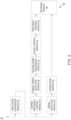
- FIG. 1 is a functional block diagram of a demodulation device according to the first embodiment of the present invention.
- FIG. 2 is a functional block diagram of an Automatic Identification System (AIS) device according to the first embodiment of the present invention.
- FIG. 3 is a diagram showing an example of the data structure of the AIS signal.
- AIS Automatic Identification System
- the AIS device 10 (for example, a universal shipborne) includes an antenna 20, a first down-conversion module 30, a coarse frequency control module 41, a symbol timing detection module 42, a second down-conversion module 43, a phase control module, a frequency tracking module 45, a signal detection module 51, a correlation module 52, and a decoding module 60.
- the modules of the AIS device 10 except the antenna 20 can be realized by an analog circuit, a digital circuit, an arithmetic processing device such as a computer, etc.
- the antenna 20 receives the AIS ([Universal Shipborne] Automatic Identification System) signal and outputs the received signal to the down conversion module 30.
- the first down-conversion module 30 down-converts the received signal to a frequency (For example, 10 times the frequency) that is a predetermined multiple of the baseband signal.
- the first down-conversion module 30 outputs the down-converted received signal to the coarse frequency control module 41 and the signal detection module 51.
- the signal for an AIS is composed of the RU data, Syncword (SW) data, Link Configuration Identity (LCID) data, the DS data, Ramp-Down (RD) data and Guard Time (GD) data.
- SW Syncword
- LCID Link Configuration Identity
- RD Ramp-Down
- GD Guard Time
- the RU data, SW data, LCID data, DS data, RD data and GD data are arranged in this order.
- the RU data, SW data, LCID data, DS data and RD data are respectively data of a prescribed number of bits and a prescribed bit array.
- the RU data, SW data and LCID data are signals that are, for example, ⁇ /4 Quadrature Phase Shift Keying (QPSK) modulated.
- DS data are signals modulated by 8 Phase Shift Keying (PSK) or 16 Quadrature Amplitude Modulation (QAM).
- the RU data is data representing the beginning of data for AIS signals.
- the SW data is data for timing detection and frequency control.
- the LCID data is data representing the modulation scheme of DS data.
- the DS data is data including various information for an AIS such as ship identification ID.
- the RD data is data for AIS signals, more specifically data representing the end of DS data.
- the GD data is a time interval left vacant, having no signal or data, during which no data is sent.
- a coarse frequency control module 41 estimates and calculates the frequency deviation from the received signal and performs coarse frequency control.
- the frequency of the reference signal is driven from a range of +/- 500 Hz to a range of +/- 30 Hz relative to the frequency of the received signal.
- the symbol timing detection module 42 detects symbol timing for the received signal after the coarse control output from the coarse frequency control module 41.
- the second down-conversion module 43 down-converts the output signal of the symbol timing detection module 42 to the baseband frequency.
- the phase control module 44 performs automatic phase control on the signal down converted to the baseband (baseband signal).
- the frequency tracking module 45 (or the demodulation device 45) performs automatic phase control and automatic frequency control with higher accuracy on the baseband signal output from the phase control module 44. This forces the frequency of the reference signal from a range of +/- 500 Hz to a range of +/- 30 Hz relative to the frequency of the received signal. Therefore, convergence to the desired symbol point can be achieved with high accuracy.
- the frequency tracking module 45 outputs the signal (demodulated signal) after the automatic phase control and the automatic frequency control to the decoding module 60. Specific details of the automatic phase control and the automatic frequency control performed by the frequency tracking module 45 will be described later.
- the frequency tracking module 45 corresponds to the "demodulation device 45" of the present invention.
- the signal detection module 51 detects RU (Ramp-Up) data of the received signal.
- the correlation module 52 uses the timing of the RU data to perform correlation processing between the received signal and the reference code.
- the correlation module 52 outputs the correlation result to the decoding module 60.
- the decoding module 60 decodes data including various information for an AIS such as a ship identification ID from Data Symbol (DS) data.
- AIS Data Symbol
- the demodulation device 45 (hereinafter interchangeably referred to as “frequency tracking module 45”) includes a Voltage-Controlled Oscillator (VCO) 451 (hereinafter interchangeably referred to as “reference signal generation module 451”), a phase rotation module 452, a phase adjustment module 453, a phase comparison module 454, and an integration module 455.
- VCO Voltage-Controlled Oscillator
- the reference signal generation module 451 adjusts a frequency of a reference signal using an integral value of a phase comparison result received from the integration module 455 to generate a frequency-adjusted reference signal.
- the reference signal generation module 451 then generates an I-Phase reference signal and a Q-Phase reference signal from the frequency-adjusted reference signal and outputs to the phase rotation module 452.
- An I-Phase signal and a Q-Phase signal of a received signal are input to the phase rotation module 452 along with the I-Phase reference signal and the Q-Phase reference signal from the reference signal generation module 451.
- the I-Phase signal and the Q-Phase signal of the received signal are generated, for example, by quadrature detection of the received signal.
- the phase rotation module 452 rotates phases of the I-Phase signal and the Q-Phase signal using the I-Phase reference signal and the Q-Phase reference signal.
- the phase rotated I-Phase signal and the phase rotated Q-Phase signal from the phase rotation module 452 are output to the decoding module 60 (See Figure 2 ) and also to the phase adjustment module 453.
- the phase adjustment module 453 adjusts the phase of the phase rotated I-Phase signal and the phase of the phase rotated Q-Phase signal. More specifically, the phase adjustment module 453 uses the "double-angle formula" to adjust the phase of the phase rotated I-Phase signal and the phase of the phase rotated Q-Phase signal.
- FIG. 4 shows the transition concept of the phase adjusted by the phase adjustment module 453.
- ⁇ represents the amount of phase shift.
- FIG. 4 further shows the case of an 8PSK modulated signal.
- the phase difference (angular difference) of symbol points adjacent to the rotation direction of the phase is ⁇ /4 (rad) and 45 (deg).
- the point of 0 + ⁇ (deg) is adjusted to 0 + 2 ⁇ (deg).
- the point of 45 + ⁇ (deg) is adjusted to 90 + 2 ⁇ (deg)
- the point of 90 + ⁇ (deg) is adjusted to 180 + 2 ⁇ (deg)
- the point of 135 + ⁇ (deg) is adjusted to 270 + 2 ⁇ (deg).
- the point of 180 + ⁇ (deg) is adjusted to 360 + 2 ⁇ (deg)
- the point of 225 + ⁇ (deg) is adjusted to 450 + 2 ⁇ (deg).
- the point of 270 + ⁇ (deg) is adjusted to 540 + 2 ⁇ (deg)
- the point of 315 + ⁇ (deg) is adjusted to 630 + 2 ⁇ (deg).
- 360 + 2 ⁇ [deg] is 0 + 2 ⁇ (+ 360) [deg]
- 450 + 2 ⁇ (deg) is 90 + 2 ⁇ (+ 360) [deg]
- 540 + 2 ⁇ (deg) is 180 + 2 ⁇ (+ 360) [deg]
- 630 + 2 ⁇ (deg) is 270 + 2 ⁇ (+ 360) [deg].
- phase difference of symbol points adjacent to the phase rotation direction after the phase adjustment is 90 degrees. That is, even at 8 PSK, the phase difference of adjacent symbol points on I-Q Coordinates is the same as QPSK.
- the processing after the phase comparison module 454 can use a processing circuit for QPSK consisting of a known simple configuration.
- the frequency tracking module 45 can realize high-precision phase control and frequency control similar to the tracking processing for QPSK.
- the phase adjustment module 453 outputs the phase adjusted I-Phase signal after phase adjustment and the phase adjusted Q-Phase signal after phase adjustment to the phase comparison module 454.
- the phase comparison module 454 compares the phase of the phase adjusted I-Phase signal with the phase of the phase adjusted Q-Phase signal. More specifically, the phase comparison module 454 calculates the phase difference between the phase adjusted I-Phase signal and the phase adjusted Q-Phase signal to generate a phase comparison result. The phase comparison module 454 outputs the phase comparison result to the integration module 455.
- the integration module 455 integrates the phase comparison result (the phase difference between the phase adjusted I-Phase signal and the phase adjusted Q-Phase signal) over a predetermined period of time to generate the integral value and outputs the integral value to the VCO 451 (or the reference signal generation module 451).
- the VCO 451 uses the integral value to adjust the phase and the frequency of the reference signal and outputs the phase and frequency adjusted reference signal to the phase rotation module 452.
- phase and frequency of the I and Q-Phase signals output from the phase rotation module 452 are driven to high accuracy. Therefore, convergence to the desired symbol point can be realized with high accuracy.
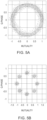
- FIG. 5A shows the pre-tracking constellation according to the first embodiment of the present invention
- FIG. 5B shows the post-tracking constellation according to the first embodiment of the present invention.
- FIG. 5A and FIG. 5B show the case where the frequency deviation is 30 Hz.
- symbol points can be detected with high precision by executing the processing of the frequency tracking module 45.
- the frequency tracking module 45 can more reliably demodulate the 8 PSK signal. Moreover, the frequency tracking module 45 can demodulate the 8 PSK signal with high accuracy.
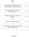
- FIG. 6 is a flow chart showing an example of a demodulation method according to an embodiment of the present invention. It should be noted that in the specific contents of each process of the flow chart shown in FIG. 6 , each module described by the explanation of the above configuration is omitted from the explanation below.
- the frequency tracking module 45 uses the reference signal (I-Phase reference signal and Q-Phase reference signal) to rotate the phases of the I-Phase signal and the Q-Phase signal of the received signal.
- the reference signal (I-Phase reference signal and Q-Phase reference signal) is set to a predetermined value, for example, assuming that there is no frequency deviation.
- the frequency tracking module 45 adjusts the phases of the phase rotated I-Phase signal and the phase rotated Q-Phase signal to generate the phase adjusted I-Phase signal and the phase adjusted Q-Phase signal.
- the phase adjustment is processing to double the phase using, for example, the "double-angle formula".
- the frequency tracking module 45 compares the phases of the phase adjusted I-Phase signal and the phase adjusted Q-Phase signal to generate the phase comparison result.
- the phase comparison processing is, for example, processing for calculating the phase difference.
- the frequency tracking module 45 integrates the phase comparison result to generate the integral value.
- the integration of the comparison results is, for example, the integral value of phase differences.
- the frequency tracking module 45 generates the reference signal using the phase comparison result. In other words, the frequency tracking module 45 performs phase adjustment and frequency adjustment of the reference signal using the integral value of the comparison results
- the frequency tracking module 45 repeatedly executes the processing from step S11 to step S 15.
- FIG. 7 is a functional block diagram of the frequency tracking module according to a second embodiment of the present invention.
- the demodulation technology of the second embodiment differs from the demodulation technology of the first embodiment in that the demodulation technology includes a frequency tracking module 45A (hereinafter interchangeably referred to as "demodulation device 45A").
- demodulation device 45A a frequency tracking module 45A (hereinafter interchangeably referred to as "demodulation device 45A").
- demodulation device 45A The other contents of the demodulation technology of the second embodiment are the same as those of the demodulation technology of the first embodiment, and each description of the same modules is omitted.
- the frequency tracking module 45A differs from the frequency tracking module 45 of the first embodiment in that it includes a gain control module 456.
- the other configuration of the frequency tracking module 45A is the same as that of the frequency tracking module 45, and each description of the same modules is omitted.
- Comparison results are input to the gain control module 456 from the phase comparison module 454.
- the gain control module 456 adjusts a gain of the phase comparison result and outputs a gain-adjusted phase comparison result to the integration module 455.
- the integration module 455 integrates the gain-adjusted phase comparison result.
- the frequency tracking module 45A can detect symbol points with high precision. Furthermore, gain adjustment is performed by the gain control module 456, so that the phase comparison result (phase difference) is corrected to a value appropriate for tracking. Thus, the frequency tracking module 45A can detect the symbol point more reliably and with higher accuracy.
- FIG. 8 is a functional block diagram of the frequency tracking module according to a third embodiment of the present invention.
- the demodulation technology according to the third embodiment differs from the demodulation technology according to the second embodiment in that a frequency tracking module 45B (hereinafter interchangeably referred to as "demodulation device 45B") is provided.
- demodulation device 45B a frequency tracking module 45B (hereinafter interchangeably referred to as "demodulation device 45B") is provided.
- the other contents of the demodulation technology according to the third embodiment are the same as those of the demodulation technology according to the third embodiment, and each description of the same modules is omitted.
- the frequency tracking module 45B differs from the frequency tracking module 45A according to the second embodiment in that it has a phase adjustment control module 457.
- the other configuration of the frequency tracking module 45B is the same as that of the frequency tracking module 45A, and each description of the same modules is omitted.
- the phase adjustment control module 457 sets an adjustment amount of the phase to the phase adjustment module 453. More specifically, the phase adjustment control module 457 sets the number of iterations of the phase adjustment using, for example, the "double-angle formula". For example, if the received signal is 8 PSK, the phase adjustment control module 457 sets the phase adjustment module 453 to perform the phase adjustment using the "double-angle formula" once. If the received signal is 16 PSK, the phase adjustment control module 457 sets the phase adjustment module 453 to perform the phase adjustment using the "double-angle formula" twice. If the received signal is 32 PSK, the phase adjustment control module 457 sets the phase adjustment module 453 to perform the phase adjustment using the "double-angle formula" three times.
- the phase adjustment module 453 performs phase adjustment according to the number of times set by the phase adjustment control module 457.
- the frequency tracking module 45B can detect symbol points with high accuracy. Furthermore, by using this configuration and processing, the frequency tracking module 45B can detect symbol points of not only 8 PSK but also other multilevel PSK signals such as 16 PSK, 32 PSK, etc., with high accuracy.
- FIG. 9A shows the pre-tracking constellation for the 16 PSK signal according to the third embodiment of the present invention
- FIG. 9B shows the post-tracking constellation for the 16 PSK signal according to the third embodiment of the present invention.
- FIG. 9A and FIG. 9B show the case where the frequency deviation is 30 Hz.
- symbol points can be detected with high precision by executing the processing of the frequency tracking module 45B.
- FIG. 10A shows the pre-tracking constellation for the 32 PSK signal according to the third embodiment of the present invention
- FIG. 10B shows the post-tracking constellation for the 32 PSK signal according to the third embodiment of the present invention.
- FIG. 10A and FIG. 10B show the case where the frequency deviation is 30 Hz.
- symbol points can be detected with high precision by executing the processing of the frequency tracking module 45B.
- the QPSK signal can also be demodulated when the phase adjustment control module 457 does not perform phase adjustment by the phase adjustment module 453, that is, sets the number of phase adjustments to zero.
- the frequency tracking module 45B can more reliably demodulate multiple types of multilevel PSK signals. Moreover, the frequency tracking module 45B can demodulate multiple types of multilevel PSK signals with high accuracy.
Landscapes
- Engineering & Computer Science (AREA)
- Computer Networks & Wireless Communication (AREA)
- Signal Processing (AREA)
- Power Engineering (AREA)
- Digital Transmission Methods That Use Modulated Carrier Waves (AREA)
Abstract
Description
- The present disclosure generally relates to a demodulation technique for multilevel (M-Ary) Phase Shift Keying (PSK) modulated signals.
-
Patent Document 1 describes a demodulation circuit for a π/4-Shift QPSK signal. - (Patent document 1)
Japanese Patent Laid-Open No. 6 -132996 - However, in the demodulation circuit described in
Patent Document 1, it is difficult to demodulate multilevel PSK signals such as 8PSK. - Therefore, there exists a need for a method or device for more reliably realizing the demodulation of multilevel PSK signals.
- A demodulation device of this invention includes a phase rotation module, a phase adjustment module, a phase comparison module, and a reference signal generation module. The phase rotation module rotates the phases of an I-Phase signal and a Q-Phase signal in a received signal of a multilevel PSK signal using a reference signal. The phase adjustment module adjusts the phases of the phase rotated I-Phase signal and the phase rotated Q-Phase signal output from the phase rotation module by multiplying the phases of the I-Phase signal and the Q-Phase signal with an integer value to generate a phase adjusted I-Phase signal and a phase adjusted Q-Phase signal. The phase comparison module compares the phase of the phase-adjusted I-Phase signal with the phase of the phase-adjusted Q-Phase signal to generate a phase comparison result. The reference signal generation module generates the reference signal using the phase comparison result.
- An advantage of various embodiments is to provide in multilevel PSK, a constant phase difference (angular difference) between symbols adjacent to the rotational direction of the phase. In this configuration, by setting the phase adjustment amount to be the predetermined value being multiplied by integer times, the phase difference (angular difference) between symbols adjacent to the rotational direction of the phase after the phase adjustment is adjusted to 45 degrees. Therefore, even a multilevel PSK such as 8 PSK, for example, can realize frequency adjustment of the reference signal in the same way as QPSK.
- According to this invention, the demodulation of multilevel PSK signals can be more reliably realized.
-
-
FIG. 1 is a functional block diagram of a demodulation device according to an embodiment of the present invention; -
FIG. 2 is a functional block diagram of an Automatic Identification System (AIS) device according to an embodiment of the present invention; -
FIG. 3 is a diagram showing an example of the data structure of a signal for an AIS; -
FIG. 4 is a diagram showing the phase transition concept adjusted by a phase adjustment module; -
FIG. 5A shows the pre-tracking constellation according to a first embodiment of the present invention, andFIG. 5B shows the post-tracking constellation according to the first embodiment of the present invention; -
FIG. 6 is a flow chart showing an example of the demodulation method according to an embodiment of the present invention; -
FIG. 7 is a functional block diagram of the demodulation device according to a second embodiment of the present invention; -
FIG. 8 is a functional block diagram of the demodulation device according to a third embodiment of the present invention; -
FIG. 9A shows the pre-tracking constellation for the 16 PSK signal according to the third embodiment of the present invention, andFIG. 9B shows the post-tracking constellation for the 16 PSK signal according to the third embodiment of the present invention; and -
FIG. 10A shows the pre-tracking constellation for the 32 PSK signal according to the third embodiment of the present invention, andFIG. 10B shows the post-tracking constellation for the 32 PSK signal according to the third embodiment of the present invention. - Demodulation technology according to a first embodiment of the present invention will be described with reference to the figures.
FIG. 1 is a functional block diagram of a demodulation device according to the first embodiment of the present invention.FIG. 2 is a functional block diagram of an Automatic Identification System (AIS) device according to the first embodiment of the present invention.FIG. 3 is a diagram showing an example of the data structure of the AIS signal. - As shown in
FIG. 2 , the AIS device 10 (for example, a universal shipborne) includes anantenna 20, a first down-conversion module 30, a coarsefrequency control module 41, a symboltiming detection module 42, a second down-conversion module 43, a phase control module, afrequency tracking module 45, asignal detection module 51, acorrelation module 52, and adecoding module 60. The modules of theAIS device 10 except theantenna 20 can be realized by an analog circuit, a digital circuit, an arithmetic processing device such as a computer, etc. - The
antenna 20 receives the AIS ([Universal Shipborne] Automatic Identification System) signal and outputs the received signal to thedown conversion module 30.. The first down-conversion module 30 down-converts the received signal to a frequency (For example, 10 times the frequency) that is a predetermined multiple of the baseband signal. The first down-conversion module 30 outputs the down-converted received signal to the coarsefrequency control module 41 and thesignal detection module 51. - As shown in
FIG. 3 , the signal for an AIS is composed of the RU data, Syncword (SW) data, Link Configuration Identity (LCID) data, the DS data, Ramp-Down (RD) data and Guard Time (GD) data. - The RU data, SW data, LCID data, DS data, RD data and GD data are arranged in this order. The RU data, SW data, LCID data, DS data and RD data are respectively data of a prescribed number of bits and a prescribed bit array. The RU data, SW data and LCID data are signals that are, for example, π/4 Quadrature Phase Shift Keying (QPSK) modulated. DS data are signals modulated by 8 Phase Shift Keying (PSK) or 16 Quadrature Amplitude Modulation (QAM).
- The RU data is data representing the beginning of data for AIS signals. The SW data is data for timing detection and frequency control. The LCID data is data representing the modulation scheme of DS data. The DS data is data including various information for an AIS such as ship identification ID. The RD data is data for AIS signals, more specifically data representing the end of DS data. The GD data is a time interval left vacant, having no signal or data, during which no data is sent.
- A coarse
frequency control module 41 estimates and calculates the frequency deviation from the received signal and performs coarse frequency control. By the processing of the coarsefrequency control module 41, for example, the frequency of the reference signal is driven from a range of +/- 500 Hz to a range of +/- 30 Hz relative to the frequency of the received signal. - The symbol
timing detection module 42 detects symbol timing for the received signal after the coarse control output from the coarsefrequency control module 41. The second down-conversion module 43 down-converts the output signal of the symboltiming detection module 42 to the baseband frequency. - The
phase control module 44 performs automatic phase control on the signal down converted to the baseband (baseband signal). - The frequency tracking module 45 (or the demodulation device 45) performs automatic phase control and automatic frequency control with higher accuracy on the baseband signal output from the
phase control module 44. This forces the frequency of the reference signal from a range of +/- 500 Hz to a range of +/- 30 Hz relative to the frequency of the received signal. Therefore, convergence to the desired symbol point can be achieved with high accuracy. Thefrequency tracking module 45 outputs the signal (demodulated signal) after the automatic phase control and the automatic frequency control to thedecoding module 60. Specific details of the automatic phase control and the automatic frequency control performed by thefrequency tracking module 45 will be described later. Thefrequency tracking module 45 corresponds to the "demodulation device 45" of the present invention. - The
signal detection module 51 detects RU (Ramp-Up) data of the received signal. Thecorrelation module 52 uses the timing of the RU data to perform correlation processing between the received signal and the reference code. Thecorrelation module 52 outputs the correlation result to thedecoding module 60. - Using the demodulation signal and the timing of detection of the main lobe of the correlation result (peak detection timing), the
decoding module 60 decodes data including various information for an AIS such as a ship identification ID from Data Symbol (DS) data. - As shown in
FIG. 1 , the demodulation device 45 (hereinafter interchangeably referred to as "frequency tracking module 45") includes a Voltage-Controlled Oscillator (VCO) 451 (hereinafter interchangeably referred to as "referencesignal generation module 451"), aphase rotation module 452, aphase adjustment module 453, aphase comparison module 454, and anintegration module 455. TheVCO 451 is synonymously referred to as "referencesignal generation module 451" of the present invention. - The reference
signal generation module 451 adjusts a frequency of a reference signal using an integral value of a phase comparison result received from theintegration module 455 to generate a frequency-adjusted reference signal. The referencesignal generation module 451 then generates an I-Phase reference signal and a Q-Phase reference signal from the frequency-adjusted reference signal and outputs to thephase rotation module 452. - An I-Phase signal and a Q-Phase signal of a received signal are input to the
phase rotation module 452 along with the I-Phase reference signal and the Q-Phase reference signal from the referencesignal generation module 451. The I-Phase signal and the Q-Phase signal of the received signal are generated, for example, by quadrature detection of the received signal. - The
phase rotation module 452 rotates phases of the I-Phase signal and the Q-Phase signal using the I-Phase reference signal and the Q-Phase reference signal. The phase rotated I-Phase signal and the phase rotated Q-Phase signal from thephase rotation module 452 are output to the decoding module 60 (SeeFigure 2 ) and also to thephase adjustment module 453. - The
phase adjustment module 453 adjusts the phase of the phase rotated I-Phase signal and the phase of the phase rotated Q-Phase signal. More specifically, thephase adjustment module 453 uses the "double-angle formula" to adjust the phase of the phase rotated I-Phase signal and the phase of the phase rotated Q-Phase signal. -
FIG. 4 shows the transition concept of the phase adjusted by thephase adjustment module 453. InFIG. 4 , θ represents the amount of phase shift. -
FIG. 4 further shows the case of an 8PSK modulated signal. In 8PSK, the phase difference (angular difference) of symbol points adjacent to the rotation direction of the phase is π/4 (rad) and 45 (deg). - Therefore, as shown in
FIG. 4 , when phase adjustment is performed by thephase adjustment module 453, the point of 0 + θ (deg) is adjusted to 0 + 2θ (deg). The point of 45 + θ (deg) is adjusted to 90 + 2θ (deg), the point of 90 + θ (deg) is adjusted to 180 + 2θ (deg), and the point of 135 + θ (deg) is adjusted to 270 + 2θ (deg). The point of 180 + θ (deg) is adjusted to 360 + 2θ (deg), and the point of 225 + θ (deg) is adjusted to 450 + 2θ (deg). The point of 270 + θ (deg) is adjusted to 540 + 2θ (deg), and the point of 315 + θ (deg) is adjusted to 630 + 2θ (deg). - Here, 360 + 2θ [deg] is 0 + 2θ (+ 360) [deg], 450 + 2θ (deg) is 90 + 2θ (+ 360) [deg], 540 + 2θ (deg) is 180 + 2θ (+ 360) [deg], and 630 + 2θ (deg) is 270 + 2θ (+ 360) [deg].
- Therefore, the phase difference of symbol points adjacent to the phase rotation direction after the phase adjustment is 90 degrees. That is, even at 8 PSK, the phase difference of adjacent symbol points on I-Q Coordinates is the same as QPSK.
- Thus, the processing after the
phase comparison module 454 can use a processing circuit for QPSK consisting of a known simple configuration. As a result, thefrequency tracking module 45 can realize high-precision phase control and frequency control similar to the tracking processing for QPSK. - The
phase adjustment module 453 outputs the phase adjusted I-Phase signal after phase adjustment and the phase adjusted Q-Phase signal after phase adjustment to thephase comparison module 454. - The
phase comparison module 454 compares the phase of the phase adjusted I-Phase signal with the phase of the phase adjusted Q-Phase signal. More specifically, thephase comparison module 454 calculates the phase difference between the phase adjusted I-Phase signal and the phase adjusted Q-Phase signal to generate a phase comparison result. Thephase comparison module 454 outputs the phase comparison result to theintegration module 455. - The
integration module 455 integrates the phase comparison result (the phase difference between the phase adjusted I-Phase signal and the phase adjusted Q-Phase signal) over a predetermined period of time to generate the integral value and outputs the integral value to the VCO 451 (or the reference signal generation module 451). - The
VCO 451 uses the integral value to adjust the phase and the frequency of the reference signal and outputs the phase and frequency adjusted reference signal to thephase rotation module 452. - By repeating the above processing, the phase and frequency of the I and Q-Phase signals output from the
phase rotation module 452 are driven to high accuracy. Therefore, convergence to the desired symbol point can be realized with high accuracy. -
FIG. 5A shows the pre-tracking constellation according to the first embodiment of the present invention, andFIG. 5B shows the post-tracking constellation according to the first embodiment of the present invention.FIG. 5A and FIG. 5B show the case where the frequency deviation is 30 Hz. - As shown in
FIG. 5A and FIG. 5B symbol points can be detected with high precision by executing the processing of thefrequency tracking module 45. - Thus, the
frequency tracking module 45 can more reliably demodulate the 8 PSK signal. Moreover, thefrequency tracking module 45 can demodulate the 8 PSK signal with high accuracy. -
FIG. 6 is a flow chart showing an example of a demodulation method according to an embodiment of the present invention. It should be noted that in the specific contents of each process of the flow chart shown inFIG. 6 , each module described by the explanation of the above configuration is omitted from the explanation below. - At
step S 11, thefrequency tracking module 45 uses the reference signal (I-Phase reference signal and Q-Phase reference signal) to rotate the phases of the I-Phase signal and the Q-Phase signal of the received signal. At the beginning of the phase adjustment processing, the reference signal (I-Phase reference signal and Q-Phase reference signal) is set to a predetermined value, for example, assuming that there is no frequency deviation. - At step S12, the
frequency tracking module 45 adjusts the phases of the phase rotated I-Phase signal and the phase rotated Q-Phase signal to generate the phase adjusted I-Phase signal and the phase adjusted Q-Phase signal. In one embodiment, the phase adjustment is processing to double the phase using, for example, the "double-angle formula". - At step S13, the
frequency tracking module 45 compares the phases of the phase adjusted I-Phase signal and the phase adjusted Q-Phase signal to generate the phase comparison result. The phase comparison processing is, for example, processing for calculating the phase difference. - At step S14, the
frequency tracking module 45 integrates the phase comparison result to generate the integral value. The integration of the comparison results is, for example, the integral value of phase differences. - At
step S 15, thefrequency tracking module 45 generates the reference signal using the phase comparison result. In other words, thefrequency tracking module 45 performs phase adjustment and frequency adjustment of the reference signal using the integral value of the comparison results - Hereafter, the
frequency tracking module 45 repeatedly executes the processing from step S11 to stepS 15. - Demodulation technology according to a second embodiment of the present invention will be described with reference to the figures.
FIG. 7 is a functional block diagram of the frequency tracking module according to a second embodiment of the present invention. - The demodulation technology of the second embodiment differs from the demodulation technology of the first embodiment in that the demodulation technology includes a
frequency tracking module 45A (hereinafter interchangeably referred to as "demodulation device 45A"). The other contents of the demodulation technology of the second embodiment are the same as those of the demodulation technology of the first embodiment, and each description of the same modules is omitted. - The
frequency tracking module 45A differs from thefrequency tracking module 45 of the first embodiment in that it includes again control module 456. The other configuration of thefrequency tracking module 45A is the same as that of thefrequency tracking module 45, and each description of the same modules is omitted. - Comparison results (for example, the phase comparison result) are input to the
gain control module 456 from thephase comparison module 454. Thegain control module 456 adjusts a gain of the phase comparison result and outputs a gain-adjusted phase comparison result to theintegration module 455. Theintegration module 455 integrates the gain-adjusted phase comparison result. - In this configuration, the
frequency tracking module 45A can detect symbol points with high precision. Furthermore, gain adjustment is performed by thegain control module 456, so that the phase comparison result (phase difference) is corrected to a value appropriate for tracking. Thus, thefrequency tracking module 45A can detect the symbol point more reliably and with higher accuracy. - Demodulation technology according to a third embodiment of the present invention will be described with reference to the figures.
FIG. 8 is a functional block diagram of the frequency tracking module according to a third embodiment of the present invention. - The demodulation technology according to the third embodiment differs from the demodulation technology according to the second embodiment in that a
frequency tracking module 45B (hereinafter interchangeably referred to as "demodulation device 45B") is provided. The other contents of the demodulation technology according to the third embodiment are the same as those of the demodulation technology according to the third embodiment, and each description of the same modules is omitted. - The
frequency tracking module 45B differs from thefrequency tracking module 45A according to the second embodiment in that it has a phase adjustment control module 457. The other configuration of thefrequency tracking module 45B is the same as that of thefrequency tracking module 45A, and each description of the same modules is omitted. - The phase adjustment control module 457 sets an adjustment amount of the phase to the
phase adjustment module 453. More specifically, the phase adjustment control module 457 sets the number of iterations of the phase adjustment using, for example, the "double-angle formula". For example, if the received signal is 8 PSK, the phase adjustment control module 457 sets thephase adjustment module 453 to perform the phase adjustment using the "double-angle formula" once. If the received signal is 16 PSK, the phase adjustment control module 457 sets thephase adjustment module 453 to perform the phase adjustment using the "double-angle formula" twice. If the received signal is 32 PSK, the phase adjustment control module 457 sets thephase adjustment module 453 to perform the phase adjustment using the "double-angle formula" three times. - The
phase adjustment module 453 performs phase adjustment according to the number of times set by the phase adjustment control module 457. - In this configuration, the
frequency tracking module 45B can detect symbol points with high accuracy. Furthermore, by using this configuration and processing, thefrequency tracking module 45B can detect symbol points of not only 8 PSK but also other multilevel PSK signals such as 16 PSK, 32 PSK, etc., with high accuracy. -
FIG. 9A shows the pre-tracking constellation for the 16 PSK signal according to the third embodiment of the present invention, andFIG. 9B shows the post-tracking constellation for the 16 PSK signal according to the third embodiment of the present invention.FIG. 9A and FIG. 9B show the case where the frequency deviation is 30 Hz. - As shown in
FIG. 9A and FIG. 9B , symbol points can be detected with high precision by executing the processing of thefrequency tracking module 45B. -
FIG. 10A shows the pre-tracking constellation for the 32 PSK signal according to the third embodiment of the present invention, andFIG. 10B shows the post-tracking constellation for the 32 PSK signal according to the third embodiment of the present invention.FIG. 10A and FIG. 10B show the case where the frequency deviation is 30 Hz. - As shown in
FIG. 10A and FIG. 10B , symbol points can be detected with high precision by executing the processing of thefrequency tracking module 45B. - The QPSK signal can also be demodulated when the phase adjustment control module 457 does not perform phase adjustment by the
phase adjustment module 453, that is, sets the number of phase adjustments to zero. - Thus, the
frequency tracking module 45B can more reliably demodulate multiple types of multilevel PSK signals. Moreover, thefrequency tracking module 45B can demodulate multiple types of multilevel PSK signals with high accuracy. -
- 10: UAIS/AIS/(Universal Shipborne) Automatic Identification System
- 20: Antenna
- 30: (First) Down Conversion Module (Down Converter)
- 41: Coarse Frequency Control Module / Coarse Frequency Controller
- 42: Symbol Timing Detection Module (Symbol Timing Detector)
- 43: Down Conversion Module (Down Converter)
- 44: Phase Control Module (Phase Controller)
- 45, 45A, 45B: Frequency Tracking Module (Frequency Tracker)
- 51: Signal Detection Module (Signal Detector)
- 52: Correlation Module (Correlator)
- 60: Decoding Module (Decoder)
- 451:VCO [Reference Signal Generation Module / Reference Signal Generator]
- 452: Phase Rotation Module (Phase Rotator)
- 453: Phase Adjustment Module (Phase Adjuster)
- 454: Phase Comparison Module (Phase Comparator)
- 455: Integration Module (integration module)
- 456: Gain Control Module (Gain Controller)
- 457: Phase Adjustment Control Module (Phase Adjustment Controller)
Claims (8)
- A demodulation device (45; 45A; 45B), comprising:a phase rotation module (452) configured to rotate phases of an I-Phase signal and a Q-Phase signal in a received signal of a multilevel PSK signal using a reference signal;a phase adjustment module (453) configured to adjust the phases of the phase rotated I-Phase signal and the phase rotated Q-Phase signal output from the phase rotation module (452) by multiplying the phases of the phase rotated I-Phase signal and the phase rotated Q-Phase signal with an integer value to generate a phase adjusted I-Phase signal and a phase adjusted Q-Phase signal;a phase comparison module (454) configured to compare the phase of the phase adjusted I-Phase signal with the phase of the phase adjusted Q-Phase signal to generate a phase comparison result; anda reference signal generation module (451) configured to generate a reference signal using the phase comparison result.
- The demodulation device (45; 45A; 45B) according to claim 1, further comprising:an integration module (455) configured to integrate the phase comparison result to generate an integral value; andthe reference signal generation module (451) is further configured to generate the reference signal using the integral value.
- The demodulation device (45; 45A; 45B) according to claim 2, further comprising:a gain control module (456) configured to adjust a gain of the phase comparison result to generate a gain-adjusted phase comparison result; andthe integration module (455) is further configured to integrate the gain-adjusted phase comparison result.
- The demodulation device (45; 45A; 45B) according to any of claims 1 to 3, wherein:
the phase adjustment module (453) is further configured to vary the integer value. - A demodulation method, comprising:rotating (S11) phases of an I-Phase signal and a Q-Phase signal in a received signal of a multilevel PSK signal using a reference signal to generate a phase-rotated I-Phase signal and a phase-rotated Q-Phase signal;adjusting (S12) the phases of the phase rotated I-Phase signal and the phase rotated Q-Phase signal by multiplying the phases of the phase rotated I-Phase signal and the phase-rotated Q-Phase signal with an integer value to generate a phase adjusted I-Phase signal and a phase adjusted Q-Phase signal;comparing (S13) the phase of the phase adjusted I-Phase signal with the phase of the phase adjusted Q-Phase signal to generate a phase comparison result; andgenerating (S15) a reference signal using the phase comparison result.
- The demodulation method according to claim 5, further comprising:integrating (S14) the phase comparison result to generate an integral value; andgenerating the reference signal using the integral value.
- The demodulation method according to claim 6, further comprising:adjusting a gain of the phase comparison result to generate a gain-adjusted phase comparison result; andintegrating the gain-adjusted phase comparison result.
- The demodulation method according to any of claims 5 to 7, further comprising:
varying the integer value.
Applications Claiming Priority (2)
| Application Number | Priority Date | Filing Date | Title |
|---|---|---|---|
| JP2021021996 | 2021-02-15 | ||
| PCT/JP2022/000460 WO2022172660A1 (en) | 2021-02-15 | 2022-01-11 | Demodulator and demodulation method |
Publications (2)
| Publication Number | Publication Date |
|---|---|
| EP4293968A1 true EP4293968A1 (en) | 2023-12-20 |
| EP4293968A4 EP4293968A4 (en) | 2025-03-05 |
Family
ID=82837738
Family Applications (1)
| Application Number | Title | Priority Date | Filing Date |
|---|---|---|---|
| EP22752493.1A Pending EP4293968A4 (en) | 2021-02-15 | 2022-01-11 | DEMODULATOR AND DEMODULATION METHOD |
Country Status (4)
| Country | Link |
|---|---|
| US (1) | US12261569B2 (en) |
| EP (1) | EP4293968A4 (en) |
| JP (1) | JP7781087B2 (en) |
| WO (1) | WO2022172660A1 (en) |
Family Cites Families (10)
| Publication number | Priority date | Publication date | Assignee | Title |
|---|---|---|---|---|
| JPH06132996A (en) | 1992-10-19 | 1994-05-13 | Fujitsu Ltd | π / 4 shift QPSK demodulation circuit |
| EP0674412B1 (en) * | 1994-03-25 | 2004-07-14 | Samsung Electronics Co., Ltd. | Method and apparatus for automatic frequency control |
| JP3147147B2 (en) * | 1996-11-22 | 2001-03-19 | 日本電気株式会社 | Carrier recovery circuit, frequency error detection method, and multi-level quadrature amplitude demodulator |
| JP3185725B2 (en) * | 1997-09-29 | 2001-07-11 | 日本電気株式会社 | Carrier recovery circuit |
| US6151368A (en) * | 1999-03-22 | 2000-11-21 | Sicom, Inc. | Phase-noise compensated digital communication receiver and method therefor |
| JP2003046587A (en) * | 2001-08-03 | 2003-02-14 | Nec Corp | Demodulator |
| JP5046114B2 (en) * | 2007-12-12 | 2012-10-10 | 日本電気株式会社 | Multilevel QAM demodulator, demodulating method thereof, and radio communication system |
| JP5578601B2 (en) * | 2009-11-05 | 2014-08-27 | 日本電気株式会社 | Carrier recovery circuit, demodulation circuit, and carrier recovery method |
| JP2013126224A (en) * | 2011-12-16 | 2013-06-24 | Nec Engineering Ltd | Clock recovery circuit, digital demodulation circuit including the same, clock recovery method, and digital demodulation method including the same |
| JP2018196000A (en) * | 2017-05-18 | 2018-12-06 | 富士通株式会社 | Reception device and frequency deviation elimination method |
-
2022
- 2022-01-11 WO PCT/JP2022/000460 patent/WO2022172660A1/en not_active Ceased
- 2022-01-11 EP EP22752493.1A patent/EP4293968A4/en active Pending
- 2022-01-11 JP JP2022581251A patent/JP7781087B2/en active Active
-
2023
- 2023-06-21 US US18/339,134 patent/US12261569B2/en active Active
Also Published As
| Publication number | Publication date |
|---|---|
| JP7781087B2 (en) | 2025-12-05 |
| EP4293968A4 (en) | 2025-03-05 |
| JPWO2022172660A1 (en) | 2022-08-18 |
| WO2022172660A1 (en) | 2022-08-18 |
| US20230336124A1 (en) | 2023-10-19 |
| US12261569B2 (en) | 2025-03-25 |
Similar Documents
| Publication | Publication Date | Title |
|---|---|---|
| US4943982A (en) | Baseband carrier phase corrector | |
| US4652834A (en) | Rapid acquisition demodulation system | |
| JP5046114B2 (en) | Multilevel QAM demodulator, demodulating method thereof, and radio communication system | |
| EP0373405B1 (en) | Automatic frequency control in the presence of data | |
| US8396433B2 (en) | Radio communication apparatus and DC offset adjustment method | |
| HK1000408B (en) | Automatic frequency control in the presence of data | |
| CN101005480B (en) | Demodulation circuit and demodulation method | |
| US20030007575A1 (en) | Demodulating device, broadcasting system, and semiconductor device | |
| EP4293968A1 (en) | Demodulator and demodulation method | |
| JP3206553B2 (en) | Demodulator | |
| US6483883B1 (en) | Automatic gain control type demodulation apparatus having single automatic gain control circuit | |
| KR101129300B1 (en) | Method for synchronizing a circuit during reception of a modulated signal | |
| US6781448B2 (en) | Method and apparatus for demodulating data | |
| US20070121762A1 (en) | Psk receiver, psk demodulating circuit, communication apparatus, and psk receiving method | |
| JP5213769B2 (en) | Receiving machine | |
| JP4292398B2 (en) | Multilevel QAM / multilevel PSK signal synchronization method and apparatus | |
| JP3206581B2 (en) | Demodulator | |
| US20040096023A1 (en) | Reduced phase error derotator system and method | |
| EP4293923A1 (en) | Timing detection device and timing detection method | |
| JP4375032B2 (en) | QAM transmission system and QAM receiver | |
| JP4438204B2 (en) | Digital demodulator | |
| JPH11355372A (en) | Frequency reproduction circuit and frequency reproduction method | |
| CN1972262A (en) | PSK receiver, PSK demodulating circuit, communication apparatus, and PSK receiving method | |
| JP3865893B2 (en) | Demodulator circuit | |
| JP2000244592A (en) | Demodulator |
Legal Events
| Date | Code | Title | Description |
|---|---|---|---|
| STAA | Information on the status of an ep patent application or granted ep patent |
Free format text: STATUS: THE INTERNATIONAL PUBLICATION HAS BEEN MADE |
|
| PUAI | Public reference made under article 153(3) epc to a published international application that has entered the european phase |
Free format text: ORIGINAL CODE: 0009012 |
|
| STAA | Information on the status of an ep patent application or granted ep patent |
Free format text: STATUS: REQUEST FOR EXAMINATION WAS MADE |
|
| 17P | Request for examination filed |
Effective date: 20230904 |
|
| AK | Designated contracting states |
Kind code of ref document: A1 Designated state(s): AL AT BE BG CH CY CZ DE DK EE ES FI FR GB GR HR HU IE IS IT LI LT LU LV MC MK MT NL NO PL PT RO RS SE SI SK SM TR |
|
| DAV | Request for validation of the european patent (deleted) | ||
| DAX | Request for extension of the european patent (deleted) | ||
| A4 | Supplementary search report drawn up and despatched |
Effective date: 20250204 |
|
| RIC1 | Information provided on ipc code assigned before grant |
Ipc: H04L 27/233 20060101ALI20250129BHEP Ipc: H04L 27/00 20060101ALI20250129BHEP Ipc: H04L 27/38 20060101ALI20250129BHEP Ipc: H03D 3/00 20060101ALI20250129BHEP Ipc: H04L 7/00 20060101ALI20250129BHEP Ipc: H04L 27/227 20060101AFI20250129BHEP |