EP4293472A1 - A clock scheme circuit - Google Patents
A clock scheme circuit Download PDFInfo
- Publication number
- EP4293472A1 EP4293472A1 EP23174151.3A EP23174151A EP4293472A1 EP 4293472 A1 EP4293472 A1 EP 4293472A1 EP 23174151 A EP23174151 A EP 23174151A EP 4293472 A1 EP4293472 A1 EP 4293472A1
- Authority
- EP
- European Patent Office
- Prior art keywords
- clock
- phase
- global
- local
- clock signal
- Prior art date
- Legal status (The legal status is an assumption and is not a legal conclusion. Google has not performed a legal analysis and makes no representation as to the accuracy of the status listed.)
- Pending
Links
Images



Classifications
-
- H—ELECTRICITY
- H03—ELECTRONIC CIRCUITRY
- H03L—AUTOMATIC CONTROL, STARTING, SYNCHRONISATION OR STABILISATION OF GENERATORS OF ELECTRONIC OSCILLATIONS OR PULSES
- H03L7/00—Automatic control of frequency or phase; Synchronisation
- H03L7/06—Automatic control of frequency or phase; Synchronisation using a reference signal applied to a frequency- or phase-locked loop
- H03L7/08—Details of the phase-locked loop
- H03L7/081—Details of the phase-locked loop provided with an additional controlled phase shifter
- H03L7/0812—Details of the phase-locked loop provided with an additional controlled phase shifter and where no voltage or current controlled oscillator is used
- H03L7/0818—Details of the phase-locked loop provided with an additional controlled phase shifter and where no voltage or current controlled oscillator is used the controlled phase shifter comprising coarse and fine delay or phase-shifting means
-
- G—PHYSICS
- G06—COMPUTING OR CALCULATING; COUNTING
- G06F—ELECTRIC DIGITAL DATA PROCESSING
- G06F1/00—Details not covered by groups G06F3/00 - G06F13/00 and G06F21/00
- G06F1/04—Generating or distributing clock signals or signals derived directly therefrom
- G06F1/10—Distribution of clock signals, e.g. skew
-
- G—PHYSICS
- G06—COMPUTING OR CALCULATING; COUNTING
- G06F—ELECTRIC DIGITAL DATA PROCESSING
- G06F1/00—Details not covered by groups G06F3/00 - G06F13/00 and G06F21/00
- G06F1/04—Generating or distributing clock signals or signals derived directly therefrom
- G06F1/08—Clock generators with changeable or programmable clock frequency
-
- G—PHYSICS
- G06—COMPUTING OR CALCULATING; COUNTING
- G06F—ELECTRIC DIGITAL DATA PROCESSING
- G06F1/00—Details not covered by groups G06F3/00 - G06F13/00 and G06F21/00
- G06F1/26—Power supply means, e.g. regulation thereof
- G06F1/32—Means for saving power
- G06F1/3203—Power management, i.e. event-based initiation of a power-saving mode
- G06F1/3234—Power saving characterised by the action undertaken
- G06F1/325—Power saving in peripheral device
- G06F1/3275—Power saving in memory, e.g. RAM, cache
-
- G—PHYSICS
- G11—INFORMATION STORAGE
- G11C—STATIC STORES
- G11C11/00—Digital stores characterised by the use of particular electric or magnetic storage elements; Storage elements therefor
- G11C11/21—Digital stores characterised by the use of particular electric or magnetic storage elements; Storage elements therefor using electric elements
- G11C11/34—Digital stores characterised by the use of particular electric or magnetic storage elements; Storage elements therefor using electric elements using semiconductor devices
- G11C11/40—Digital stores characterised by the use of particular electric or magnetic storage elements; Storage elements therefor using electric elements using semiconductor devices using transistors
- G11C11/401—Digital stores characterised by the use of particular electric or magnetic storage elements; Storage elements therefor using electric elements using semiconductor devices using transistors forming cells needing refreshing or charge regeneration, i.e. dynamic cells
- G11C11/4063—Auxiliary circuits, e.g. for addressing, decoding, driving, writing, sensing or timing
- G11C11/407—Auxiliary circuits, e.g. for addressing, decoding, driving, writing, sensing or timing for memory cells of the field-effect type
- G11C11/4076—Timing circuits
-
- G—PHYSICS
- G11—INFORMATION STORAGE
- G11C—STATIC STORES
- G11C7/00—Arrangements for writing information into, or reading information out from, a digital store
- G11C7/22—Read-write [R-W] timing or clocking circuits; Read-write [R-W] control signal generators or management
- G11C7/222—Clock generating, synchronizing or distributing circuits within memory device
-
- H—ELECTRICITY
- H03—ELECTRONIC CIRCUITRY
- H03L—AUTOMATIC CONTROL, STARTING, SYNCHRONISATION OR STABILISATION OF GENERATORS OF ELECTRONIC OSCILLATIONS OR PULSES
- H03L7/00—Automatic control of frequency or phase; Synchronisation
- H03L7/06—Automatic control of frequency or phase; Synchronisation using a reference signal applied to a frequency- or phase-locked loop
- H03L7/08—Details of the phase-locked loop
- H03L7/099—Details of the phase-locked loop concerning mainly the controlled oscillator of the loop
- H03L7/0995—Details of the phase-locked loop concerning mainly the controlled oscillator of the loop the oscillator comprising a ring oscillator
- H03L7/0998—Details of the phase-locked loop concerning mainly the controlled oscillator of the loop the oscillator comprising a ring oscillator using phase interpolation
-
- H—ELECTRICITY
- H03—ELECTRONIC CIRCUITRY
- H03L—AUTOMATIC CONTROL, STARTING, SYNCHRONISATION OR STABILISATION OF GENERATORS OF ELECTRONIC OSCILLATIONS OR PULSES
- H03L7/00—Automatic control of frequency or phase; Synchronisation
- H03L7/06—Automatic control of frequency or phase; Synchronisation using a reference signal applied to a frequency- or phase-locked loop
- H03L7/16—Indirect frequency synthesis, i.e. generating a desired one of a number of predetermined frequencies using a frequency- or phase-locked loop
- H03L7/18—Indirect frequency synthesis, i.e. generating a desired one of a number of predetermined frequencies using a frequency- or phase-locked loop using a frequency divider or counter in the loop
- H03L7/1806—Indirect frequency synthesis, i.e. generating a desired one of a number of predetermined frequencies using a frequency- or phase-locked loop using a frequency divider or counter in the loop the frequency divider comprising a phase accumulator generating the frequency divided signal
-
- G—PHYSICS
- G11—INFORMATION STORAGE
- G11C—STATIC STORES
- G11C2207/00—Indexing scheme relating to arrangements for writing information into, or reading information out from, a digital store
- G11C2207/22—Control and timing of internal memory operations
- G11C2207/2254—Calibration
Definitions
- the present invention relates to a clock scheme circuit, and, in particular, to a high-speed mobile double data rate memory (DDR).
- DDR mobile double data rate memory
- Mobile DDR also known as MDDR, Low Power DDR or LPDDR
- MDDR Low Power DDR
- LPDDR Low Power DDR
- its clock scheme circuit may consume too much power.
- a low-power clock circuit scheme is called for.
- a clock scheme circuit with low power consumption is proposed.
- a clock scheme circuit in accordance with an exemplary embodiment of the present invention has a global clock generator, a global clock trace, and a local clock generator.
- the local clock generator is coupled to the global clock generator through the global clock trace to receive a global clock signal, and thereby generates a local clock signal based on the global clock signal.
- the local clock generator has a frequency multiplier.
- the local clock generator generating the local clock signal uses the frequency multiplier to multiply the frequency of the global clock signal by a multiplication factor of not less than 1. In this manner, the global clock signal can be a low-frequency signal in comparison with the local clock signal. Less power is consumed along the global clock trace. The power efficiency of the clock scheme circuit is great.
- the frequency multiplier is provided by a multiplying delay-locked loop (MDLL).
- the frequency multiplier is provided by a circuit that multiples the frequency by 1 (e.g., a delay-locked loop (DLL), or a phase-looked loop (PLL)).
- DLL delay-locked loop
- PLL phase-looked loop
- the local clock generator further has a multi-phase generator provides the frequency multiplier.
- the multi-phase generator generates split-phase clock signals to be processed to generate the local clock signal.
- the local clock generator further has a plurality of phase selection multiplexers and a phase interpolator.
- Each phase selection multiplexer receives several of the split-phase clock signals to output selected two split-phase clock signals.
- the phase interpolator is coupled to output terminals of the phase selection multiplexers to perform phase interpolation on split-phase clock signals selected by the phase selection multiplexers, for generation of the local clock signal.
- the local clock generator further has a driver, receiving a phase-interpolated clock signal from the phase interpolator to generate and output the local clock signal.
- the driver has a frequency divider, dividing the frequency of the phase-interpolated clock signal to generate the local clock signal.
- the local clock generator further has a phase selection multiplexer, receiving all of the split-phase clock signals to output one selected split-phase clock signal for generation of the local clock signal.
- the local clock generator does not use any phase interpolator that consumes considerable power.
- the local clock generator further has a driver, receiving the selected split-phase clock signal from the phase selection multiplexer to generate and output the local clock signal.
- the driver has a frequency divider, dividing the frequency of the selected split-phase clock signal to generate the local clock signal.
- the global clock generator uses just one phase-locked loop (PLL) to generate the global clock signal.
- PLL phase-locked loop
- the frequency multiplier within the local clock generator is switched to provide different multiplication factors to multiply the frequency of the global clock signal, and the multiplication factors all are not less than one.
- the global clock generator uses multiple phase-locked loops (PLLs) to generate multiple global clock candidates.
- PLLs phase-locked loops
- a clock gating multiplexer is provided on the global clock trace to select one of the global clock candidates as the global clock signal to be transferred to the local clock generator.
- the local clock generator is coupled to a functional unit with a local clock trace, and the global trace is longer than the local clock trace.
- the global trace may be X times longer than the local clock trace.
- a mobile double data rate memory which includes a DQ unit and the forgoing clock scheme circuit.
- the DQ unit has a transmitter and a receiver.
- the clock scheme circuit provides the local clock signal to the transmitter, the receiver, or both through a local clock trace.
- FIG. 1 depicts a mobile double data rate memory (abbreviated as MDDR, or LPDDR) 100 in accordance with an exemplary embodiment of the present invention.
- MDDR mobile double data rate memory
- the mobile double data rate memory 100 has a DQ unit 102 and a clock scheme circuit 104.
- the DQ unit 102 may correspond to a memory cell, for read/write of the memory cell.
- the DQ unit 102 has a transmitter TX and a receiver RX for read/write data from/into the memory cell.
- the transmitter TX and/or the receiver RX operate according to a local clock signal Local_Clk provided by the clock scheme circuit 104.
- the clock scheme circuit 104 has a global clock generator 106, a global clock trace 108, and a local clock generator 110.
- the local clock generator 110 is coupled to the global clock generator 106 through the global clock trace 108 to receive a global clock signal Global_Clk.
- the local clock generator 110 generates the local clock signal Local_Clk based on the global clock signal Global_Clk and the local clock signal Local_Clk is transferred to the DQ unit 102 through a local clock trace 109.
- the global clock signal Global_Clk is a single phase signal.
- the local clock generator 110 has a frequency multiplier 112, which is provided to multiply the frequency of the global clock signal Global_Clk by a multiplication factor (M) of not less than 1, for generation of the local clock signal Local_Clk. Because the local clock generator 110 has the frequency multiplier 112, the global clock signal Global_Clk transferred from the global clock generator 106 to the local clock generator 110 through the global clock trace 108 can be a low-frequency signal in comparison with the local clock signal Local_Clk transferred from the local clock generator 110 to the DQ unit 102 through the local clock trace 109.
- the local clock signal Local_Clk should be very high for operations of the transmitter/receiver (TX/RX) of the DQ unit 102.
- the local clock trace 109 is shorter than the global clock trace.
- the length of the global clock trace 108 is more than 10 times longer than the length of the local clock trace. That said, the higher frequency local clock signal Local_Clk travels shorter length of the local clock trace 109, and the lower frequency global clock signal Global_Clk travels longer length of the global clock trace 108. With such design of the present embodiment, the less power is consumed on the global clock trace 108. The power efficiency of the clock scheme circuit 100 is improved.
- the DQ unit 102 may be replaced by any functional unit.
- the length of the global trace 108 is X times longer than the length of the local clock trace, X is a number greater than 1.
- the frequency multiplier 112 is provided by a multiplying delay-locked loop (MDLL).
- MDLL multiplying delay-locked loop
- the multiplication factor (M) introduced by the frequency multiplier 112 is greater than one, and the global clock signal Global_Clk transferred from the global clock generator 106 to the local clock generator 110 through the global clock trace 108, therefore, oscillates at a very low frequency.
- the power consumption of the global clock trace 108 is considerably reduced.
- the frequency multiplier 112 is provided by a delay-locked loop (DLL) or a phase-looked loop (PLL).
- the multiplication factor (M) introduced by the frequency multiplier 112 is one.
- the DLL/PLL with the multiplication factor, 1 allows the global clock signal Global_Clk has a reasonable oscillation frequency rather than a very high frequency. The power consumption of the global clock trace 108 is reduced, too.
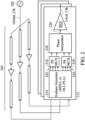
- FIG. 2 illustrates the details of the clock scheme circuit 104 in accordance with an exemplary embodiment of the present invention. Three layers of circuits are shown in FIG. 2 ; two layers for data TX/RX, and one layer for command TX/RX.
- the global clock trace 204 may include an AC coupled device for power domain transformation, clock gating (CG) elements, flyby elements (e.g., buffers), and duty cycle correctors (DCC).
- the global clock signal Global_Clk generated by the single oscillator 202 is transferred to the local clock generator 212 through the global clock trace 204. Because the global clock signal Global_Clk oscillates at the lower frequency than a conventional technique, the global clock trace 204 operates at the lower frequency and saves considerable power.
- the local clock generator 212 has an 8-phase generator 214, two phase selection multiplexers 216 and 218, a phase interpolator 220, and a driver BUF (e.g., an ARBUF).
- the 8-phase generator 214 may be a multiplying delay-locked loop (MDLL) or a delay-locked loop (DLL)/phase-locked loop (PLL), which implements the function of the frequency multiplier 112 of FIG. 1 , and generates split-phase clock signals (the four signals indicated by 222 and the other four signals indicated by 224).
- the phase selection multiplexer 216 receives the split-phase clock signals 222 to output the selected two split-phase clock signals.
- the phase selection multiplexer 218 receives the split-phase clock signals 224 to output the selected two split-phase clock signals.
- the phase interpolator 220 is coupled to the output terminals of the phase selection multiplexers 216 and 218 to perform phase interpolation on the split-phase clock signals selected by the phase selection multiplexers 216 and 218.
- the driver BUF receives a phase-interpolated clock signal 226 from the phase interpolator 220 to generate and output the local clock signal Local_Clk.
- the single oscillator 202 generates a single phase global clock signal Global_Clk.
- the driver BUF may have a function of frequency divider, dividing (x1, x0.5, ...) the frequency of the phase-interpolated clock signal 226 to provide more frequency options for the local clock signal Local_Clk.
- an MDLL can be quickly switched to provide the different multiplication factors (e.g., x1 or x8) for frequency multiplying. Because the MDLL implementing the 8-phasegenerator 214 can quickly change its multiplication factor, there is no need to use several PLLs in the global clock generator 116 to generate several global clock candidates (e.g., one PLL generating 1G clock, and another PLL generating 500M clock) to be selected and transferred as the global clock signal Global_Clk.
- the global clock generator 106 can use just one PLL (202). Less power is required.
- the circuit area of a single PLL is smaller than two PLLs. The circuit cost is low.
- the PLL 202 generates the global clock signal Global_Clk oscillating at 1G Hz.
- the 8-phase generator 214 implemented by an MDLL provides two options for the multiplication factor: one is x8, and the other is x4.
- the local clock signal Local_Clk may oscillate at 8G Hz (or a frequency that the buffer BUF divides from 8GHz) or be switched to oscillate at 4G Hz (or a frequency that the buffer BUF divides from 4GHz). It is suitable to use such a clock scheme circuit in a high speed LPDDR.
- FIG. 3 illustrates a variant of the clock scheme circuit of FIG. 2 in accordance with an exemplary embodiment of the present invention.
- Two PLLs 302 and 304 are used to implement the global clock generator 106.
- the PLL 302 may generate a 1G clock
- the PLL 304 may generate a 500M clock.
- the 1G clock and the 500M clock are global clock candidates, and one of them is selected by the clock gating multiplexer 306 to be the global clock signal Global_Clk to be transferred to the local clock generator 308.
- the 8-phase generator 310 in the local clock generator 308 may be an MDLL that provides a fixed multiplication factor, such as x8.
- x8 a fixed multiplication factor
- FIG. 3 although one more PLL (in compared with FIG. 2 ) is required to implement the global clock generator 106, the clock scheme circuit of FIG. 3 still has the capability to provide various local clock signals as the clock scheme circuit of FIG. 2 .
- FIG. 4 illustrates a clock scheme circuit in accordance with another exemplary embodiment of the present invention.
- the local clock generator 402 has a 64-phase generator 404, a phase selection multiplexer 406, and a driver BUF.
- the 64-phase generator 404 may be implemented by an MDLL or a DLL/PLL, which provides the function of frequency multiplier and generates 64 split-phase clock signals 408.
- the phase selection multiplexer 406 receives all of the 64 split-phase clock signals 408, and outputs one selected split-phase clock signal 410 to the driver BUF.
- the driver BUF may have the function of frequency divider, dividing (x1, x0.5, ...) the frequency of the selected split-phase clock signal 410 to provide more frequency options for the local clock signal Local_Clk.
- phase interpolator 220 In comparison with the local clock generator 212 of FIG. 2 , the local clock generator 402 of FIG. 4 does not use the phase interpolator 220 that consumes considerable power.
- the phase selection multiplexer 406 may be implemented by a group of multiplexer switches (abbreviated as PS MUX GP). The glitch and PVT sensitive problems due to the phase interpolator 220, therefore, are solved.
- the 64-phase generator 404 implemented by an MDLL can be switched between different multiplication factors for frequency multiplying, and only one PLL 412 is required to implement the global clock generator 106.
- the PLL 412 generates the global clock signal Global_Clk oscillating at 1G Hz.
- the 64-phase generator 404 implemented by an MDLL provides two options for the multiplication factor: one is x8, and the other is x4.
- the local clock signal Local_Clk may oscillate at 8G Hz (or a frequency that the buffer BUF divides from 8GHz) or be switched to oscillate at 4G Hz (or a frequency that the buffer BUF divides from 4GHz). It is suitable to use such a clock scheme circuit in a high speed LPDDR.
- the global clock generator 106 may use multiple PLLs.
- FIG. 5 illustrates a variant of the clock scheme circuit of FIG. 4 in accordance with an exemplary embodiment of the present invention.
- Two PLLs 502 and 504 are used to implement the global clock generator 106.
- the PLL 502 may generate a 1G clock
- the PLL 504 may generate a 500M clock.
- the 1G clock and the 500M clock are global clock candidates, and one of them is selected by the clock gating multiplexer 506 to be the global clock signal Global_Clk to be transferred to the local clock generator 508.
- the 64-phase generator 510 in the local clock generator 508 may be an MDLL that provides a fixed multiplication factor, such as x8.
- the clock scheme circuit of FIG. 5 still provides various local clock signals as the clock scheme circuit of FIG. 4 .
- FIG. 6 illustrates how to use a DLL to implement the 8-phase generator 214 (or 310) in accordance with an exemplary embodiment of the present invention.
- the global clock signal Global_Clk transferred from the global clock generator 106 to the local clock generator 110 through the global clock trance 108 is CKref, and after being delayed by the delay cells, 8 split-phase clock signals CK0, CK45, CK90, CK135, CK180, CK225, CK270, and CK315 are generated to be sent to the phase selection multiplexers 216 and 218.
- the 8 split-phase clock signals CK0, CK45, CK90, CK135, CK180, CK225, CK270, and CK315 oscillate at the same frequency as the global clock signal CKref.
- more delay cells are added to the 8-phase generator of FIG. 6 to form the 64-phase generator 404 of FIG. 4 (or 510 of FIG. 5 ).
- 64 delay cells are required, and 64 split-phase clock signals are generated to be sent to the phase selection multiplexer 406.
- FIG. 7 illustrates how to use an MDLL to implement the 8-phase generator 214 (or 310) in accordance with an exemplary embodiment of the present invention.
- the global clock signal Global_Clk transferred from the global clock generator 106 to the local clock generator 110 through the global clock trance 108 is CKref.
- the global clock signal CKref and the clock signal CK315 are selectively sent to the delay cells, and after being delayed by the delay cells, 8 split-phase clock signals CK0, CK45, CK90, CK135, CK180, CK225, CK270, and CK315 are generated.
- the 8 split-phase clock signals CK0, CK45, CK90, CK135, CK180, CK225, CK270, and CK315 oscillate at the multiple times of frequency of the global clock signal CKref.
- more delay cells are added to the 8-phase generator of FIG. 7 to form the 64-phase generator 404 of FIG. 4 (or 510 of FIG. 5 ).
- 64 delay cells are required.
- the frequency multiplier 112 may be implemented by a multi-phase generator (e.g., the 8-phase generator 214 and the 64-phase generator 510).
- the multi-phase generator may be an MDLL, DLL, or PLL to benefit from their background calibration capability.
Landscapes
- Engineering & Computer Science (AREA)
- Theoretical Computer Science (AREA)
- Physics & Mathematics (AREA)
- General Engineering & Computer Science (AREA)
- General Physics & Mathematics (AREA)
- Microelectronics & Electronic Packaging (AREA)
- Computer Hardware Design (AREA)
- Manipulation Of Pulses (AREA)
- Mobile Radio Communication Systems (AREA)
Abstract
Description
- The present invention relates to a clock scheme circuit, and, in particular, to a high-speed mobile double data rate memory (DDR).
- Mobile DDR (also known as MDDR, Low Power DDR or LPDDR) is a type of DDR SDRAM, specially used in mobile electronic products, such as smartphones, etc. In a mobile DDR, such a high-speed design, its clock scheme circuit may consume too much power.
- A low-power clock circuit scheme is called for.
- A clock scheme circuit with low power consumption is proposed.
- A clock scheme circuit in accordance with an exemplary embodiment of the present invention has a global clock generator, a global clock trace, and a local clock generator. The local clock generator is coupled to the global clock generator through the global clock trace to receive a global clock signal, and thereby generates a local clock signal based on the global clock signal. The local clock generator has a frequency multiplier. The local clock generator generating the local clock signal uses the frequency multiplier to multiply the frequency of the global clock signal by a multiplication factor of not less than 1. In this manner, the global clock signal can be a low-frequency signal in comparison with the local clock signal. Less power is consumed along the global clock trace. The power efficiency of the clock scheme circuit is great.
- In an exemplary embodiment, the frequency multiplier is provided by a multiplying delay-locked loop (MDLL). In another exemplary embodiment, the frequency multiplier is provided by a circuit that multiples the frequency by 1 (e.g., a delay-locked loop (DLL), or a phase-looked loop (PLL)).
- In an exemplary embodiment, the local clock generator further has a multi-phase generator provides the frequency multiplier. The multi-phase generator generates split-phase clock signals to be processed to generate the local clock signal.
- In an exemplary embodiment, the local clock generator further has a plurality of phase selection multiplexers and a phase interpolator. Each phase selection multiplexer receives several of the split-phase clock signals to output selected two split-phase clock signals. The phase interpolator is coupled to output terminals of the phase selection multiplexers to perform phase interpolation on split-phase clock signals selected by the phase selection multiplexers, for generation of the local clock signal. In an exemplary embodiment, the local clock generator further has a driver, receiving a phase-interpolated clock signal from the phase interpolator to generate and output the local clock signal. In an exemplary embodiment, the driver has a frequency divider, dividing the frequency of the phase-interpolated clock signal to generate the local clock signal.
- In another exemplary embodiment, the local clock generator further has a phase selection multiplexer, receiving all of the split-phase clock signals to output one selected split-phase clock signal for generation of the local clock signal. In such an exemplary embodiment, the local clock generator does not use any phase interpolator that consumes considerable power. In an exemplary embodiment, the local clock generator further has a driver, receiving the selected split-phase clock signal from the phase selection multiplexer to generate and output the local clock signal. In an exemplary embodiment, the driver has a frequency divider, dividing the frequency of the selected split-phase clock signal to generate the local clock signal.
- In an exemplary embodiment, the global clock generator uses just one phase-locked loop (PLL) to generate the global clock signal. The frequency multiplier within the local clock generator is switched to provide different multiplication factors to multiply the frequency of the global clock signal, and the multiplication factors all are not less than one.
- In another exemplary embodiment, the global clock generator uses multiple phase-locked loops (PLLs) to generate multiple global clock candidates. A clock gating multiplexer is provided on the global clock trace to select one of the global clock candidates as the global clock signal to be transferred to the local clock generator.
- In an exemplary embodiment, the local clock generator is coupled to a functional unit with a local clock trace, and the global trace is longer than the local clock trace. The global trace may be X times longer than the local clock trace.
- In an exemplary embodiment, a mobile double data rate memory is shown, which includes a DQ unit and the forgoing clock scheme circuit. The DQ unit has a transmitter and a receiver. The clock scheme circuit provides the local clock signal to the transmitter, the receiver, or both through a local clock trace.
- A detailed description is given in the following embodiments with reference to the accompanying drawings.
- The present invention can be more fully understood by reading the subsequent detailed description and examples with references made to the accompanying drawings, wherein:
-
FIG. 1 depicts a mobile double data rate memory (abbreviated as MDDR, or LPDDR) 100 in accordance with an exemplary embodiment of the present invention; -
FIG. 2 illustrates the details of theclock scheme circuit 104 in accordance with an exemplary embodiment of the present invention; -
FIG. 3 illustrates a variant of the clock scheme circuit ofFIG. 2 in accordance with an exemplary embodiment of the present invention; -
FIG. 4 illustrates a clock scheme circuit in accordance with another exemplary embodiment of the present invention; -
FIG. 5 illustrates a variant of the clock scheme circuit ofFIG. 4 in accordance with an exemplary embodiment of the present invention; -
FIG. 6 illustrates how to use a DLL to implement the 8-phase generator 214 in accordance with an exemplary embodiment of the present invention; and -
FIG. 7 illustrates how to use an MDLL to implement the 8-phase generator 214 in accordance with an exemplary embodiment of the present invention. - The following description is made for the purpose of illustrating the general principles of the invention and should not be taken in a limiting sense. The scope of the invention is best determined by reference to the appended claims.
-
FIG. 1 depicts a mobile double data rate memory (abbreviated as MDDR, or LPDDR) 100 in accordance with an exemplary embodiment of the present invention. - The mobile double
data rate memory 100 has aDQ unit 102 and aclock scheme circuit 104. TheDQ unit 102 may correspond to a memory cell, for read/write of the memory cell. TheDQ unit 102 has a transmitter TX and a receiver RX for read/write data from/into the memory cell. The transmitter TX and/or the receiver RX operate according to a local clock signal Local_Clk provided by theclock scheme circuit 104. - The
clock scheme circuit 104 has aglobal clock generator 106, aglobal clock trace 108, and alocal clock generator 110. Thelocal clock generator 110 is coupled to theglobal clock generator 106 through theglobal clock trace 108 to receive a global clock signal Global_Clk. Thelocal clock generator 110 generates the local clock signal Local_Clk based on the global clock signal Global_Clk and the local clock signal Local_Clk is transferred to theDQ unit 102 through alocal clock trace 109. In the present embodiment, the global clock signal Global_Clk is a single phase signal. Especially, thelocal clock generator 110 has afrequency multiplier 112, which is provided to multiply the frequency of the global clock signal Global_Clk by a multiplication factor (M) of not less than 1, for generation of the local clock signal Local_Clk. Because thelocal clock generator 110 has thefrequency multiplier 112, the global clock signal Global_Clk transferred from theglobal clock generator 106 to thelocal clock generator 110 through theglobal clock trace 108 can be a low-frequency signal in comparison with the local clock signal Local_Clk transferred from thelocal clock generator 110 to theDQ unit 102 through thelocal clock trace 109. The local clock signal Local_Clk should be very high for operations of the transmitter/receiver (TX/RX) of theDQ unit 102. In the present embodiment, thelocal clock trace 109 is shorter than the global clock trace. In some embodiments, the length of theglobal clock trace 108 is more than 10 times longer than the length of the local clock trace. That said, the higher frequency local clock signal Local_Clk travels shorter length of thelocal clock trace 109, and the lower frequency global clock signal Global_Clk travels longer length of theglobal clock trace 108. With such design of the present embodiment, the less power is consumed on theglobal clock trace 108. The power efficiency of theclock scheme circuit 100 is improved. In some exemplary embodiments, theDQ unit 102 may be replaced by any functional unit. In some exemplary embodiments, the length of theglobal trace 108 is X times longer than the length of the local clock trace, X is a number greater than 1. - In an exemplary embodiment, the
frequency multiplier 112 is provided by a multiplying delay-locked loop (MDLL). In such a case, the multiplication factor (M) introduced by thefrequency multiplier 112 is greater than one, and the global clock signal Global_Clk transferred from theglobal clock generator 106 to thelocal clock generator 110 through theglobal clock trace 108, therefore, oscillates at a very low frequency. The power consumption of theglobal clock trace 108 is considerably reduced. - In another exemplary embodiment, the
frequency multiplier 112 is provided by a delay-locked loop (DLL) or a phase-looked loop (PLL). In such a case, the multiplication factor (M) introduced by thefrequency multiplier 112 is one. In comparison with a conventional technology that uses a frequency divider to reduce the frequency of a highfrequency global clock signal for local use, the DLL/PLL with the multiplication factor, 1, allows the global clock signal Global_Clk has a reasonable oscillation frequency rather than a very high frequency. The power consumption of theglobal clock trace 108 is reduced, too. -
FIG. 2 illustrates the details of theclock scheme circuit 104 in accordance with an exemplary embodiment of the present invention. Three layers of circuits are shown inFIG. 2 ; two layers for data TX/RX, and one layer for command TX/RX. - In
FIG. 2 , there is a single oscillator 202 (e.g. a phase-locked loop, abbreviated as PLL) for implementation of theglobal clock generator 106 ofFig. 1 . Theglobal clock trace 204 may include an AC coupled device for power domain transformation, clock gating (CG) elements, flyby elements (e.g., buffers), and duty cycle correctors (DCC). The global clock signal Global_Clk generated by thesingle oscillator 202 is transferred to thelocal clock generator 212 through theglobal clock trace 204. Because the global clock signal Global_Clk oscillates at the lower frequency than a conventional technique, theglobal clock trace 204 operates at the lower frequency and saves considerable power. Thelocal clock generator 212 has an 8-phase generator 214, twophase selection multiplexers phase interpolator 220, and a driver BUF (e.g., an ARBUF). The 8-phase generator 214 may be a multiplying delay-locked loop (MDLL) or a delay-locked loop (DLL)/phase-locked loop (PLL), which implements the function of thefrequency multiplier 112 ofFIG. 1 , and generates split-phase clock signals (the four signals indicated by 222 and the other four signals indicated by 224). Thephase selection multiplexer 216 receives the split-phase clock signals 222 to output the selected two split-phase clock signals. Thephase selection multiplexer 218 receives the split-phase clock signals 224 to output the selected two split-phase clock signals. Thephase interpolator 220 is coupled to the output terminals of thephase selection multiplexers phase selection multiplexers clock signal 226 from thephase interpolator 220 to generate and output the local clock signal Local_Clk. Moreover, thesingle oscillator 202 generates a single phase global clock signal Global_Clk. - In some exemplary embodiments, the driver BUF may have a function of frequency divider, dividing (x1, x0.5, ...) the frequency of the phase-interpolated
clock signal 226 to provide more frequency options for the local clock signal Local_Clk. - Especially, an MDLL can be quickly switched to provide the different multiplication factors (e.g., x1 or x8) for frequency multiplying. Because the MDLL implementing the 8-
phasegenerator 214 can quickly change its multiplication factor, there is no need to use several PLLs in the global clock generator 116 to generate several global clock candidates (e.g., one PLL generating 1G clock, and another PLL generating 500M clock) to be selected and transferred as the global clock signal Global_Clk. Theglobal clock generator 106 can use just one PLL (202). Less power is required. Furthermore, the circuit area of a single PLL is smaller than two PLLs. The circuit cost is low. - In an exemplary embodiment, the
PLL 202 generates the global clock signal Global_Clk oscillating at 1G Hz. The 8-phase generator 214 implemented by an MDLL provides two options for the multiplication factor: one is x8, and the other is x4. Thus, the local clock signal Local_Clk may oscillate at 8G Hz (or a frequency that the buffer BUF divides from 8GHz) or be switched to oscillate at 4G Hz (or a frequency that the buffer BUF divides from 4GHz). It is suitable to use such a clock scheme circuit in a high speed LPDDR. - If the 8-
phase generator 214 implemented by an MDLL does not provide several options for the multiplication factor, theglobal clock generator 106 may use multiple PLLs.FIG. 3 illustrates a variant of the clock scheme circuit ofFIG. 2 in accordance with an exemplary embodiment of the present invention. TwoPLLs global clock generator 106. ThePLL 302 may generate a 1G clock, and thePLL 304 may generate a 500M clock. The 1G clock and the 500M clock are global clock candidates, and one of them is selected by theclock gating multiplexer 306 to be the global clock signal Global_Clk to be transferred to thelocal clock generator 308. The 8-phase generator 310 in thelocal clock generator 308 may be an MDLL that provides a fixed multiplication factor, such as x8. InFIG. 3 , although one more PLL (in compared withFIG. 2 ) is required to implement theglobal clock generator 106, the clock scheme circuit ofFIG. 3 still has the capability to provide various local clock signals as the clock scheme circuit ofFIG. 2 . -
FIG. 4 illustrates a clock scheme circuit in accordance with another exemplary embodiment of the present invention. In comparison with thelocal clock generator 212 ofFIG. 2 , a more power-savinglocal clock generator 402 is shown. Thelocal clock generator 402 has a 64-phase generator 404, aphase selection multiplexer 406, and a driver BUF. The 64-phase generator 404 may be implemented by an MDLL or a DLL/PLL, which provides the function of frequency multiplier and generates 64 split-phase clock signals 408. Thephase selection multiplexer 406 receives all of the 64 split-phase clock signals 408, and outputs one selected split-phase clock signal 410 to the driver BUF. The driver BUF may have the function of frequency divider, dividing (x1, x0.5, ...) the frequency of the selected split-phase clock signal 410 to provide more frequency options for the local clock signal Local_Clk. - In comparison with the
local clock generator 212 ofFIG. 2 , thelocal clock generator 402 ofFIG. 4 does not use thephase interpolator 220 that consumes considerable power. Thephase selection multiplexer 406 may be implemented by a group of multiplexer switches (abbreviated as PS MUX GP). The glitch and PVT sensitive problems due to thephase interpolator 220, therefore, are solved. - In an exemplary embodiment, the 64-
phase generator 404 implemented by an MDLL can be switched between different multiplication factors for frequency multiplying, and only onePLL 412 is required to implement theglobal clock generator 106. - In an exemplary embodiment, the
PLL 412 generates the global clock signal Global_Clk oscillating at 1G Hz. The 64-phase generator 404 implemented by an MDLL provides two options for the multiplication factor: one is x8, and the other is x4. Thus, the local clock signal Local_Clk may oscillate at 8G Hz (or a frequency that the buffer BUF divides from 8GHz) or be switched to oscillate at 4G Hz (or a frequency that the buffer BUF divides from 4GHz). It is suitable to use such a clock scheme circuit in a high speed LPDDR. - If the 64-
phase generator 404 implemented by an MDLL does not provide several options for the multiplication factor, theglobal clock generator 106 may use multiple PLLs. -
FIG. 5 illustrates a variant of the clock scheme circuit ofFIG. 4 in accordance with an exemplary embodiment of the present invention. TwoPLLs global clock generator 106. ThePLL 502 may generate a 1G clock, and thePLL 504 may generate a 500M clock. The 1G clock and the 500M clock are global clock candidates, and one of them is selected by theclock gating multiplexer 506 to be the global clock signal Global_Clk to be transferred to thelocal clock generator 508. The 64-phase generator 510 in thelocal clock generator 508 may be an MDLL that provides a fixed multiplication factor, such as x8. Although one more PLL is required in theglobal clock generator 106, the clock scheme circuit ofFIG. 5 still provides various local clock signals as the clock scheme circuit ofFIG. 4 . -
FIG. 6 illustrates how to use a DLL to implement the 8-phase generator 214 (or 310) in accordance with an exemplary embodiment of the present invention. There are 8 delay cells, each outputs a split-phase clock signal. As shown, the global clock signal Global_Clk transferred from theglobal clock generator 106 to thelocal clock generator 110 through theglobal clock trance 108 is CKref, and after being delayed by the delay cells, 8 split-phase clock signals CK0, CK45, CK90, CK135, CK180, CK225, CK270, and CK315 are generated to be sent to thephase selection multiplexers - In another exemplary embodiment, more delay cells are added to the 8-phase generator of
FIG. 6 to form the 64-phase generator 404 ofFIG. 4 (or 510 ofFIG. 5 ). To implement the 64-phase generator 404 ofFIG. 4 , 64 delay cells are required, and 64 split-phase clock signals are generated to be sent to thephase selection multiplexer 406. -
FIG. 7 illustrates how to use an MDLL to implement the 8-phase generator 214 (or 310) in accordance with an exemplary embodiment of the present invention. There are 8 delay cells, each outputs a split-phase clock signal (CK0, CK45, CK90, CK135, CK180, CK225, CK270, or CK315). As shown, the global clock signal Global_Clk transferred from theglobal clock generator 106 to thelocal clock generator 110 through theglobal clock trance 108 is CKref. The global clock signal CKref and the clock signal CK315 are selectively sent to the delay cells, and after being delayed by the delay cells, 8 split-phase clock signals CK0, CK45, CK90, CK135, CK180, CK225, CK270, and CK315 are generated. According to such an MDLL design, the 8 split-phase clock signals CK0, CK45, CK90, CK135, CK180, CK225, CK270, and CK315 oscillate at the multiple times of frequency of the global clock signal CKref. - In another exemplary embodiment, more delay cells are added to the 8-phase generator of
FIG. 7 to form the 64-phase generator 404 ofFIG. 4 (or 510 ofFIG. 5 ). To implement the 64-phase generator 404 ofFIG. 4 , 64 delay cells are required. - Any clock scheme circuit having the
frequency multiplier 112 in thelocal clock generator 110 should be considered within the scope of the invention. Thefrequency multiplier 112 may be implemented by a multi-phase generator (e.g., the 8-phase generator 214 and the 64-phase generator 510). The multi-phase generator may be an MDLL, DLL, or PLL to benefit from their background calibration capability. - While the invention has been described by way of example and in terms of the preferred embodiments, it should be understood that the invention is not limited to the disclosed embodiments. On the contrary, it is intended to cover various modifications and similar arrangements (as would be apparent to those skilled in the art). Therefore, the scope of the appended claims should be accorded the broadest interpretation so as to encompass all such modifications and similar arrangements.
Claims (15)
- A clock scheme circuit (104), characterized in comprising:a global clock generator (106) and a global clock trace (108); anda local clock generator (110), coupled to the global clock generator through the global clock trace to receive a global clock signal (Global_Clk), and generate a local clock signal (Local_Clk) based on the global clock signal,wherein:the local clock generator comprises a frequency multiplier (112); andthe local clock generator generating the local clock signal uses the frequency multiplier to multiply a frequency of the global clock signal by a multiplication factor of not less than 1.
- The clock scheme circuit as claimed in claim 1, wherein:
the frequency multiplier is provided by a multiplying delay-locked loop, a delay-locked loop or a phase-locked loop (214/310/404/510/FIG. 6/FIG/ 7). - The clock scheme circuit as claimed in claim 1 or 2, wherein the local clock generator further comprises:
a multi-phase generator (214/310/404/510/FIG. 6/FIG. 7), providing the frequency multiplier, and generating split-phase clock signals to be processed to generate the local clock signal. - The clock scheme circuit as claimed in claim 3, wherein the local clock generator further comprises:a plurality of phase selection multiplexers (216 and 218); anda phase interpolator (220);wherein:each phase selection multiplexer receives several of the split-phase clock signals to output selected two split-phase clock signals; andthe phase interpolator is coupled to output terminals of the phase selection multiplexers to perform phase interpolation on split-phase clock signals selected by the phase selection multiplexers, for generation of the local clock signal.
- The clock scheme circuit as claimed in claim 4, wherein the local clock generator further comprises:
a driver (BUF), receiving a phase-interpolated clock signal from the phase interpolator to generate and output the local clock signal. - The clock scheme circuit as claimed in claim 5, wherein the driver comprises:
a frequency divider, dividing a frequency of the phase-interpolated clock signal to generate the local clock signal. - The clock scheme circuit as claimed in claim 5 or 6, wherein:the multi-phase generator (214/310) generates 8 split-phase clock signals; andtwo phase selection multiplexers (216 and 218) are provided, and each phase selection multiplexer receives 4 split-phase clock signals.
- The clock scheme circuit as claimed in claim 3, wherein the local clock generator further comprises:
a phase selection multiplexer (406), receiving all of the split-phase clock signals to output one selected split-phase clock signal for generation of the local clock signal. - The clock scheme circuit as claimed in claim 8, wherein the local clock generator further comprises:
a driver (BUF), receiving the selected split-phase clock signal from the phase selection multiplexer to generate and output the local clock signal. - The clock scheme circuit as claimed in claim 9, wherein the driver comprises:
a frequency divider, dividing a frequency of the selected split-phase clock signal to generate the local clock signal. - The clock scheme circuit as claimed in claim 9 or 10, wherein:
the multi-phase generator (404/510) generates 64 split-phase clock signals. - The clock scheme circuit as claimed in any one of the preceding claims, wherein:the global clock generator (202/412) uses just one phase-locked loop to generate the global clock signal; andthe frequency multiplier (214/404) within the local clock generator is switched to provide different multiplication factors to multiply the frequency of the global clock signal, and the multiplication factors all are not less than one.
- The clock scheme circuit as claimed in any one of claims 1 to 11, wherein:the global clock generator uses multiple phase-locked (302 and 304/502 and 504) loops to generate multiple global clock candidates; anda clock gating multiplexer (306/506) is provided on the global clock trace to select one of the global clock candidates as the global clock signal to be transferred to the local clock generator.
- The clock scheme circuit as claimed in any one of the preceding claims, wherein the local clock generator is coupled to a functional unit with a local clock trace (109), and the global trace is longer than the local clock trace.
- The clock scheme circuit as claimed in claim 14, wherein the global trace is X times longer than the local clock trace, and X is a number greater than 1.
Applications Claiming Priority (2)
| Application Number | Priority Date | Filing Date | Title |
|---|---|---|---|
| US202263351916P | 2022-06-14 | 2022-06-14 | |
| US18/170,088 US12063043B2 (en) | 2022-06-14 | 2023-02-16 | Clock scheme circuit and a mobile double data rate memory using the clock scheme circuit |
Publications (1)
| Publication Number | Publication Date |
|---|---|
| EP4293472A1 true EP4293472A1 (en) | 2023-12-20 |
Family
ID=86426102
Family Applications (1)
| Application Number | Title | Priority Date | Filing Date |
|---|---|---|---|
| EP23174151.3A Pending EP4293472A1 (en) | 2022-06-14 | 2023-05-18 | A clock scheme circuit |
Country Status (3)
| Country | Link |
|---|---|
| US (1) | US12063043B2 (en) |
| EP (1) | EP4293472A1 (en) |
| TW (1) | TWI863348B (en) |
Citations (4)
| Publication number | Priority date | Publication date | Assignee | Title |
|---|---|---|---|---|
| WO2012158392A2 (en) * | 2011-05-17 | 2012-11-22 | Rambus Inc. | Memory system using asymmetric source-synchronous clocking |
| US20130055004A1 (en) * | 2011-08-31 | 2013-02-28 | Kleanthes Koniaris | Hardware-based automatic clock gating |
| EP3170262A1 (en) * | 2014-07-18 | 2017-05-24 | Qualcomm Incorporated | Clock synchronization |
| WO2022119909A1 (en) * | 2020-12-01 | 2022-06-09 | Ciena Corporation | Apparatus and methods for low power clock generation in multi-channel high speed devices |
Family Cites Families (5)
| Publication number | Priority date | Publication date | Assignee | Title |
|---|---|---|---|---|
| US8072253B2 (en) * | 2006-09-13 | 2011-12-06 | Nec Corporation | Clock adjusting circuit and semiconductor integrated circuit device |
| JP2008217947A (en) * | 2007-03-07 | 2008-09-18 | Elpida Memory Inc | Semiconductor memory |
| KR100891335B1 (en) * | 2007-07-02 | 2009-03-31 | 삼성전자주식회사 | Clock generator capable of performing bit error rate measurements |
| JP2015149669A (en) * | 2014-02-07 | 2015-08-20 | 富士通株式会社 | Clock control circuit, receiver and communication device |
| US10171089B2 (en) * | 2016-11-17 | 2019-01-01 | Taiwan Semiconductor Manufacturing Co., Ltd. | PVT-free calibration function using a doubler circuit for TDC resolution in ADPLL applications |
-
2023
- 2023-02-16 US US18/170,088 patent/US12063043B2/en active Active
- 2023-05-18 EP EP23174151.3A patent/EP4293472A1/en active Pending
- 2023-06-14 TW TW112122172A patent/TWI863348B/en active
Patent Citations (4)
| Publication number | Priority date | Publication date | Assignee | Title |
|---|---|---|---|---|
| WO2012158392A2 (en) * | 2011-05-17 | 2012-11-22 | Rambus Inc. | Memory system using asymmetric source-synchronous clocking |
| US20130055004A1 (en) * | 2011-08-31 | 2013-02-28 | Kleanthes Koniaris | Hardware-based automatic clock gating |
| EP3170262A1 (en) * | 2014-07-18 | 2017-05-24 | Qualcomm Incorporated | Clock synchronization |
| WO2022119909A1 (en) * | 2020-12-01 | 2022-06-09 | Ciena Corporation | Apparatus and methods for low power clock generation in multi-channel high speed devices |
Non-Patent Citations (1)
| Title |
|---|
| YOON JUNSUB ET AL: "A MDLL-based multi-phase clock multiplier", 2016 INTERNATIONAL SOC DESIGN CONFERENCE (ISOCC), IEEE, 23 October 2016 (2016-10-23), pages 247 - 248, XP033032447, [retrieved on 20161227], DOI: 10.1109/ISOCC.2016.7799770 * |
Also Published As
| Publication number | Publication date |
|---|---|
| TWI863348B (en) | 2024-11-21 |
| US20230412174A1 (en) | 2023-12-21 |
| TW202349390A (en) | 2023-12-16 |
| US12063043B2 (en) | 2024-08-13 |
Similar Documents
| Publication | Publication Date | Title |
|---|---|---|
| US8164371B2 (en) | Duty detection circuit, clock generation circuit including the duty detection circuit, and semiconductor device | |
| US9818462B1 (en) | Apparatuses and methods for providing internal clock signals of different clock frequencies in a memory device | |
| CN102904553B (en) | Dynamic frequency control using coarse clock gating | |
| KR20110014230A (en) | Multiphase Clock Generator and Method | |
| KR100516742B1 (en) | Clock synchronization device | |
| US8482331B2 (en) | Open loop type delay locked loop and method for operating the same | |
| US20080238504A1 (en) | Phase locked loop | |
| US7525363B2 (en) | Delay line and delay lock loop | |
| US8294499B2 (en) | Clock signal generation circuit for reducuing current consumption, and semiconductor device having the same | |
| WO2012078818A1 (en) | Method and apparatus for frequency synthesizing | |
| CN101018049B (en) | delay locked loop | |
| US8558594B2 (en) | Reduced frequency clock delivery with local recovery | |
| US20030197536A1 (en) | Method and apparatus for synthesizing a clock signal using a compact and low power delay locked loop (dll) | |
| US12063043B2 (en) | Clock scheme circuit and a mobile double data rate memory using the clock scheme circuit | |
| US9118458B1 (en) | Clock phase alignment | |
| US6377071B1 (en) | Composite flag generation for DDR FIFOs | |
| US7424087B2 (en) | Clock divider | |
| US7953998B2 (en) | Clock generation circuit and semiconductor memory apparatus having the same | |
| CN117238339A (en) | Clock scheme circuits and associated mobile double data rate memories | |
| US11108383B1 (en) | Clock phase control | |
| Höppner et al. | An open-loop clock generator for fast frequency scaling in 65nm CMOS technology | |
| US7362156B2 (en) | Reliable phase adjustment circuit | |
| Liran et al. | All-digital dll architecture and applications | |
| US7643580B2 (en) | Signal generator circuit having multiple output frequencies | |
| KR100464399B1 (en) | Internal Clock Signal Generator and Method for Synchronous Storage |
Legal Events
| Date | Code | Title | Description |
|---|---|---|---|
| PUAI | Public reference made under article 153(3) epc to a published international application that has entered the european phase |
Free format text: ORIGINAL CODE: 0009012 |
|
| STAA | Information on the status of an ep patent application or granted ep patent |
Free format text: STATUS: THE APPLICATION HAS BEEN PUBLISHED |
|
| AK | Designated contracting states |
Kind code of ref document: A1 Designated state(s): AL AT BE BG CH CY CZ DE DK EE ES FI FR GB GR HR HU IE IS IT LI LT LU LV MC ME MK MT NL NO PL PT RO RS SE SI SK SM TR |
|
| STAA | Information on the status of an ep patent application or granted ep patent |
Free format text: STATUS: REQUEST FOR EXAMINATION WAS MADE |
|
| 17P | Request for examination filed |
Effective date: 20240619 |
|
| RBV | Designated contracting states (corrected) |
Designated state(s): AL AT BE BG CH CY CZ DE DK EE ES FI FR GB GR HR HU IE IS IT LI LT LU LV MC ME MK MT NL NO PL PT RO RS SE SI SK SM TR |
|
| STAA | Information on the status of an ep patent application or granted ep patent |
Free format text: STATUS: EXAMINATION IS IN PROGRESS |
|
| 17Q | First examination report despatched |
Effective date: 20251211 |