EP4293418A2 - Lichtemittierende vorrichtung - Google Patents
Lichtemittierende vorrichtung Download PDFInfo
- Publication number
- EP4293418A2 EP4293418A2 EP23206572.2A EP23206572A EP4293418A2 EP 4293418 A2 EP4293418 A2 EP 4293418A2 EP 23206572 A EP23206572 A EP 23206572A EP 4293418 A2 EP4293418 A2 EP 4293418A2
- Authority
- EP
- European Patent Office
- Prior art keywords
- light emitting
- light
- emitting device
- lights
- state
- Prior art date
- Legal status (The legal status is an assumption and is not a legal conclusion. Google has not performed a legal analysis and makes no representation as to the accuracy of the status listed.)
- Granted
Links
Images




Classifications
-
- F—MECHANICAL ENGINEERING; LIGHTING; HEATING; WEAPONS; BLASTING
- F21—LIGHTING
- F21V—FUNCTIONAL FEATURES OR DETAILS OF LIGHTING DEVICES OR SYSTEMS THEREOF; STRUCTURAL COMBINATIONS OF LIGHTING DEVICES WITH OTHER ARTICLES, NOT OTHERWISE PROVIDED FOR
- F21V14/00—Controlling the distribution of the light emitted by adjustment of elements
- F21V14/003—Controlling the distribution of the light emitted by adjustment of elements by interposition of elements with electrically controlled variable light transmissivity, e.g. liquid crystal elements or electrochromic devices
-
- G—PHYSICS
- G02—OPTICS
- G02F—OPTICAL DEVICES OR ARRANGEMENTS FOR THE CONTROL OF LIGHT BY MODIFICATION OF THE OPTICAL PROPERTIES OF THE MEDIA OF THE ELEMENTS INVOLVED THEREIN; NON-LINEAR OPTICS; FREQUENCY-CHANGING OF LIGHT; OPTICAL LOGIC ELEMENTS; OPTICAL ANALOGUE/DIGITAL CONVERTERS
- G02F1/00—Devices or arrangements for the control of the intensity, colour, phase, polarisation or direction of light arriving from an independent light source, e.g. switching, gating or modulating; Non-linear optics
- G02F1/01—Devices or arrangements for the control of the intensity, colour, phase, polarisation or direction of light arriving from an independent light source, e.g. switching, gating or modulating; Non-linear optics for the control of the intensity, phase, polarisation or colour
- G02F1/13—Devices or arrangements for the control of the intensity, colour, phase, polarisation or direction of light arriving from an independent light source, e.g. switching, gating or modulating; Non-linear optics for the control of the intensity, phase, polarisation or colour based on liquid crystals, e.g. single liquid crystal display cells
- G02F1/133—Constructional arrangements; Operation of liquid crystal cells; Circuit arrangements
- G02F1/1333—Constructional arrangements; Manufacturing methods
- G02F1/1334—Constructional arrangements; Manufacturing methods based on polymer dispersed liquid crystals, e.g. microencapsulated liquid crystals
-
- G—PHYSICS
- G02—OPTICS
- G02F—OPTICAL DEVICES OR ARRANGEMENTS FOR THE CONTROL OF LIGHT BY MODIFICATION OF THE OPTICAL PROPERTIES OF THE MEDIA OF THE ELEMENTS INVOLVED THEREIN; NON-LINEAR OPTICS; FREQUENCY-CHANGING OF LIGHT; OPTICAL LOGIC ELEMENTS; OPTICAL ANALOGUE/DIGITAL CONVERTERS
- G02F1/00—Devices or arrangements for the control of the intensity, colour, phase, polarisation or direction of light arriving from an independent light source, e.g. switching, gating or modulating; Non-linear optics
- G02F1/01—Devices or arrangements for the control of the intensity, colour, phase, polarisation or direction of light arriving from an independent light source, e.g. switching, gating or modulating; Non-linear optics for the control of the intensity, phase, polarisation or colour
- G02F1/13—Devices or arrangements for the control of the intensity, colour, phase, polarisation or direction of light arriving from an independent light source, e.g. switching, gating or modulating; Non-linear optics for the control of the intensity, phase, polarisation or colour based on liquid crystals, e.g. single liquid crystal display cells
- G02F1/1323—Arrangements for providing a switchable viewing angle
-
- G—PHYSICS
- G02—OPTICS
- G02F—OPTICAL DEVICES OR ARRANGEMENTS FOR THE CONTROL OF LIGHT BY MODIFICATION OF THE OPTICAL PROPERTIES OF THE MEDIA OF THE ELEMENTS INVOLVED THEREIN; NON-LINEAR OPTICS; FREQUENCY-CHANGING OF LIGHT; OPTICAL LOGIC ELEMENTS; OPTICAL ANALOGUE/DIGITAL CONVERTERS
- G02F1/00—Devices or arrangements for the control of the intensity, colour, phase, polarisation or direction of light arriving from an independent light source, e.g. switching, gating or modulating; Non-linear optics
- G02F1/01—Devices or arrangements for the control of the intensity, colour, phase, polarisation or direction of light arriving from an independent light source, e.g. switching, gating or modulating; Non-linear optics for the control of the intensity, phase, polarisation or colour
- G02F1/13—Devices or arrangements for the control of the intensity, colour, phase, polarisation or direction of light arriving from an independent light source, e.g. switching, gating or modulating; Non-linear optics for the control of the intensity, phase, polarisation or colour based on liquid crystals, e.g. single liquid crystal display cells
- G02F1/133—Constructional arrangements; Operation of liquid crystal cells; Circuit arrangements
- G02F1/1333—Constructional arrangements; Manufacturing methods
- G02F1/1335—Structural association of cells with optical devices, e.g. polarisers or reflectors
- G02F1/1336—Illuminating devices
- G02F1/133602—Direct backlight
- G02F1/133606—Direct backlight including a specially adapted diffusing, scattering or light controlling members
- G02F1/133607—Direct backlight including a specially adapted diffusing, scattering or light controlling members the light controlling member including light directing or refracting elements, e.g. prisms or lenses
-
- H—ELECTRICITY
- H10—SEMICONDUCTOR DEVICES; ELECTRIC SOLID-STATE DEVICES NOT OTHERWISE PROVIDED FOR
- H10H—INORGANIC LIGHT-EMITTING SEMICONDUCTOR DEVICES HAVING POTENTIAL BARRIERS
- H10H20/00—Individual inorganic light-emitting semiconductor devices having potential barriers, e.g. light-emitting diodes [LED]
- H10H20/80—Constructional details
- H10H20/85—Packages
- H10H20/855—Optical field-shaping means, e.g. lenses
-
- H—ELECTRICITY
- H10—SEMICONDUCTOR DEVICES; ELECTRIC SOLID-STATE DEVICES NOT OTHERWISE PROVIDED FOR
- H10K—ORGANIC ELECTRIC SOLID-STATE DEVICES
- H10K59/00—Integrated devices, or assemblies of multiple devices, comprising at least one organic light-emitting element covered by group H10K50/00
- H10K59/50—OLEDs integrated with light modulating elements, e.g. with electrochromic elements, photochromic elements or liquid crystal elements
-
- H—ELECTRICITY
- H10—SEMICONDUCTOR DEVICES; ELECTRIC SOLID-STATE DEVICES NOT OTHERWISE PROVIDED FOR
- H10W—GENERIC PACKAGES, INTERCONNECTIONS, CONNECTORS OR OTHER CONSTRUCTIONAL DETAILS OF DEVICES COVERED BY CLASS H10
- H10W90/00—Package configurations
Definitions
- the present disclosure relates to a light emitting device which can control or change direction of light.
- the electronic devices such as display devices or light emitting devices can provide more convenient information transmission or image display.
- the users attach importance to privacy when viewing these devices, or as the safety requirements to prevent specific persons from viewing these devices are increased (e.g., prevent the driver from watching the display device or the light emitting device of the car while driving, or prevent the lights emitted by the display device or the light emitting device of the car from being projected on the windshield to interfere with the driver), these devices need to have the function of controlling the direction of light.
- the present disclosure aims at providing a light emitting device having a light controller for controlling or adjusting the light direction emitted from the light emitting element, so as to enhance the privacy of viewing and/or prevent specific persons from viewing.
- the claimed light emitting device includes a plurality of light emitting elements and a light controller.
- the light emitting elements are emitting lights.
- the light controller is disposed on the light emitting elements for the lights passing through, which is switchable in a first state and a second state.
- the light controller collimates the lights in the first state and diffuses the lights in the second state.
- the claimed light emitting device includes a plurality of light emitting elements and a light controller.
- the light emitting elements are emitting lights.
- the light controller is disposed on the light emitting elements.
- the light controller includes a plurality of cells for the light from the light emitting elements passing through and a plurality of walls surrounding the cells. The walls are switchable in states of a transmissive state and a non-transmissive state.
- the corresponding component such as layer or area
- it may be directly on this another component, or other component(s) may exist between them.
- the component is referred to “directly on another component (or the variant thereof)" any component does not exist between them.
- the corresponding component and the another component have a disposition relationship along a top-view/vertical direction
- the corresponding component may be below or above the another component, and the disposition relationship along the top-view/vertical direction are determined by an orientation of the device.
- first, second, third, etc. may be used to describe diverse constituent elements, such constituent elements are not limited by the terms. These terms are used only to discriminate a constituent element from other constituent elements in the specification, and these terms have no relation to the manufacturing order of these constituent components.
- the claims may not use the same terms, but instead may use the terms first, second, third, etc. with respect to the order in which an element is claimed. Accordingly, in the following description, a first constituent element may be a second constituent element in a claim.
- the light emitting device may optionally include a display function, a sensing function, a touch sensing function, an antenna function, other suitable function or a combination thereof, but not limited thereto.
- the light emitting device may include a tiled device, but not limited thereto.
- the light emitting device may include liquid crystal (LC) molecules, an organic light-emitting diode (OLED), an inorganic light-emitting diode (LED) such as a micro-LED and/or a mini-LED, quantum dots (QDs) material, a quantum-dot light-emitting diode (QLED, QDLED), fluorescence material, phosphor material, other suitable material or a combination thereof, but not limited thereto.
- LC liquid crystal
- OLED organic light-emitting diode
- LED inorganic light-emitting diode
- QDs quantum dots
- QLED, QDLED quantum-dot light-emitting diode
- fluorescence material phospho
- the light emitting device may include a color light emitting device or a monochrome light emitting device, and a shape of the light emitting device may be a rectangle, a circle, a polygon, a shape having a curved edge or other suitable shape, but not limited thereto.
- the light emitting device is a color light emitting device having light-emitting diodes (e.g., organic light-emitting diodes, inorganic light-emitting diodes or quantum-dot light-emitting diodes) as an example, but the light emitting device is not limited thereto.
- the light emitting device may include a liquid crystal panel or be other suitable light emitting device.
- FIG. 1 is a schematic diagram showing a top view of a light emitting device according to a first embodiment of the present disclosure
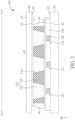
- FIG. 2 is a schematic diagram showing a cross-sectional view of the light emitting device taken along a cross-sectional line A-A' in FIG. 1
- the light emitting device 100 of this embodiment includes a first substrate 110, a plurality of light emitting elements 120, a light controller 130, a first control electrode E1 and a second control electrode E2, and the light emitting device 100 may optionally include a second substrate 140.
- the light emitting device 100 may optionally include a second substrate 140.
- the first substrate 110 may be disposed opposite to the second substrate 140, and the light emitting elements 120, the light controller 130, the first control electrode E1 and the second control electrode E2 may be disposed between the first substrate 110 and the second substrate 140.
- the first substrate 110 and the second substrate 140 may individually include glass, quartz, sapphire, polyimide (PI), polyethylene terephthalate (PET), other suitable material or a combination thereof, so as to be a rigid substrate or a flexible substrate, but not limited thereto.
- the material of the first substrate 110 and the material of the second substrate 140 may be the same or different.
- the light emitting device 100 has an illuminating surface LS
- the illuminating surface LS is an outermost surface which the light provided from the light emitting device 100 passes through.
- the illuminating surface LS may be an outer surface of the second substrate 140, but not limited thereto.
- the light emitting elements 120 may be disposed on the first substrate 110, and may be configured to emit lights. Note that, in the lights generated by the light emitting elements 120, the present disclosure only discusses the lights emitted towards the illuminating surface LS, wherein the emitted direction of the light emitted towards the illuminating surface LS has a positive component parallel to a upward normal direction Dn of the first substrate 110 (hereafter, referred as the normal direction Dn), and the lights emitted towards the illuminating surface LS may be lights directly emitted from the light emitting elements 120 and/or reflected lights emitted from the light emitting elements 120 and reflected by other component(s).
- the light emitting element 120 may generate the light with the intensity corresponding to the signal (e.g., gray level signal). For instance, if the light emitting device 100 is configured to display an image, each light emitting element 120 may generate the light with the intensity corresponding to the gray level signal of the image.
- the light emitting element 120 may be a self-luminous type component, such as an organic light-emitting diode, an inorganic light-emitting diode (e.g., micro-LED and/or a mini-LED) or a quantum-dot light-emitting diode, but not limited thereto.
- the light emitting element 120 may be corresponding to a sub-pixel in a liquid crystal panel.
- the light emitting element 120 may adjust the liquid crystal molecules in the light emitting element 120 according to the gray level signal of the image, such that the transmittance of the backlight may be adjusted, and the light emitting element 120 may generate the light with the intensity corresponding to the gray level signal of the image, but not limited thereto.
- the first substrate 110 of the light emitting device 100 may be a substrate having a driving circuit configured to drive the liquid crystal molecules in the liquid crystal panel.
- the light emitting elements 120 may generate the lights with a plurality of colors.
- the light emitting elements 120 may include at least one first light emitting element emitting red light, at least one second light emitting element emitting green light and at least one third light emitting element emitting blue light, such that the light emitting device 100 may generate colored light to be a colored light emitting device, but not limited thereto.
- the light emitting elements 120 may emit red light, green light, blue light and yellow light, but not limited thereto.
- all of the light emitting elements 120 may emit the same color light
- the light emitting device 100 may further include a light converting layer disposed on the light emitting element 120, so as to convert (or filter) the light emitted from the light emitting element 120 into another light with different color, wherein the light converting layer may be disposed at any suitable position between the illuminating surface LS and the light emitting element 120.
- the light converting layer may include color filter, quantum dots (QD) material, fluorescence material, phosphorescence material, other suitable material or a combination thereof.
- the light emitting elements 120 may emit white light, and the light converting layer may include a first light converting part converting the white light into the red light, a second light converting part converting the white light into the green light and a third light converting part converting the white light into the blue light, such that the light emitting device 100 may generate colored light to be a colored light emitting device, but not limited thereto.
- the light emitting elements 120 may emit blue light, and the light converting layer may include a first light converting part converting the blue light into the red light and a second light converting part converting the blue light into the green light, such that the light emitting device 100 may generate colored light to be a colored light emitting device, but not limited thereto.
- all of the light emitting elements 120 may emit the same color light, such that the light emitting device 100 may be a monochrome light emitting device, but not limited thereto.
- the light emitting device 100 may further include at least one switching component (not shown in figures), and each switching component may be electrically connected to one or more light emitting element(s) 120, or electrically connected to one or more component(s) in the light emitting element(s) 120, wherein the light emitting element 120 may change the intensity of its emitting light according to the switching state of the switching component which it is electrically connected.
- the switching component may be a thin film transistor (TFT) or other suitable switch, wherein the thin film transistor may be such as a top gate thin film transistor, a bottom gate thin film transistor, a dual gate thin film transistor or other suitable transistor.
- the light emitting device 100 may further include a plurality of conductive lines to be electrically connected to the electronic component(s) in the light emitting device 100.
- the conductive lines may include a plurality of first conductive lines 111 and a plurality of second conductive lines 112 disposed on the first substrate 110.
- Each first conductive line 111 may be electrically connected to or coupled to such as the light emitting element(s) 120, the component(s) in the light emitting element(s) 120 and/or the switching component(s)
- each second conductive line 112 may be electrically connected to or coupled to such as the light emitting element(s) 120, the component(s) in the light emitting element(s) 120 and/or the switching component(s).
- the first conductive line 111 may be electrically connected between one end (e.g., a source) of the switching component and a circuit (e.g., an integrated circuit) providing the gray level signal, such that the first conductive line 111 may serve as a signal line or a data line;
- the second conductive line 112 may be electrically connected between another end (e.g., a gate) of the switching component and a circuit (e.g., an integrated circuit and/or a gate driving circuit) providing a switching signal, such that the second conductive line 112 may serve as a scan line, but not limited thereto.
- the connection of the conductive line may be adjusted based on the circuit design.
- the light emitting element 120 may generate the light having the intensity corresponding to the gray level signal.
- the first conductive line 111 and the second conductive line 112 may be a line which has slight waves and substantially extends along a direction rather than a straight line.
- the first conductive lines 111 may be substantially parallel to each other
- the second conductive lines 112 may be substantially parallel to each other
- the first conductive line 111 and the second conductive line 112 may not be parallel to each other.
- the first conductive line 111 and the second conductive line 112 may be substantially perpendicular to each other, but not limited thereto.
- the light emitting device 100 may optionally include an insulating layer 150 disposed on the light emitting element(s) 120.
- the insulating layer 150 may have a protecting function to protect the light emitting element(s) 120 covered by the insulating layer 150.
- the insulating layer 150 may be further disposed on the switching component(s) and the conductive line(s), so as to protect the switching component(s) and the conductive line(s).
- the light emitting device 100 may include a circuit component layer disposed on the first substrate 110, wherein the circuit component layer may include a plurality of layers, and these layers may form the light emitting element 120, the switching component, the conductive line (e.g., the first conductive line 111 and/or the second conductive line 112) and the insulating layer 150.
- the layers in the circuit component layer may include at least one conductive layer, at least one interlayer insulating layer, at least one semiconductor layer, other suitable layer or a combination thereof.
- the material of the conductive layer may include metal, transparent conductive material (such as indium tin oxide (ITO), indium zinc oxide (IZO), etc.), other suitable conductive material or a combination thereof.
- the material of the interlayer insulating layer may include such as silicon oxide (SiO x ), silicon nitride (SiN y ), silicon oxynitride (SiO x N y ), polymethylmetacrylate (PMMA), other suitable insulating material or a combination thereof.
- the material of the semiconductor layer may include such as poly-silicon, amorphous silicon, metal-oxide semiconductor (e.g., IGZO), other suitable semiconductor material or a combination thereof, but not limited thereto.
- These layers in the circuit component layer may be formed by at least one semiconductor process(es) such as a deposition process, an etch process and/or a photolithography.
- the light emitting element 120 for example, but not limited to, the organic light-emitting diode
- the switching component for example, but not limited to, the organic light-emitting diode
- the conductive line and the insulating layer 150 may be formed by the semiconductor process(es), but not limited thereto.
- the layers in the circuit component layer may form the switching component and the conductive line, and the light emitting element 120 (for example, but not limited to, the inorganic light-emitting diode) may be disposed on the circuit component layer by a bonding process; then, the insulating layer 150 is formed on the light emitting element 120, but not limited thereto.
- the layers in the circuit component layer may form the switching component, the conductive line and at least one component of the light emitting element 120, and other component(s) of the light emitting element 120 may be formed on the circuit component layer by other suitable method(s).
- the light emitting element 120 is the sub-pixel in the liquid crystal panel
- a pixel electrode of the light emitting element 120 may be included in the circuit component layer, and the liquid crystal molecules are disposed on the circuit component layer.
- the insulating layer 150 may be another substrate of the liquid crystal panel, and this another substrate is opposite to the substrate having the driving circuit configured to drive the liquid crystal molecules.
- the layers in the circuit component layer may be further configured to form other required electronic component(s) and/or structure(s).
- the light emitting device 100 may further include other required active component(s) and/or passive component(s) disposed in the circuit component layer.
- the light emitting device 100 may further include a capacitor, and the capacitor may be electrically connected to the light emitting element 120 or the component(s) of the light emitting element 120, but not limited thereto.
- the light controller 130, the first control electrode E1 and the second control electrode E2 are disposed on the light emitting elements 120, wherein the first control electrode E1 and the second control electrode E2 may control the state of the light controller 130 based on the received control signal.
- the lights generated by the light emitting elements 120 may have different types of radiating directions after they pass through the light controller 130. In some embodiments (as shown in FIG.
- the light controller 130 may include a plurality of switchable diffusers 132 and a plurality of light shielding elements 134, wherein the switchable diffuser 132 may be disposed corresponding to (or overlapped with) at least one of the light emitting elements 120 in the normal direction Dn, and the light shielding element 134 may be disposed between two adjacent switchable diffusers 132. Therefore, the light shielding element 134 may be not corresponding to (or not overlapped with) the light emitting element 120 in the normal direction Dn.
- the switchable diffuser 132 may be corresponding to (or overlapped with) one light emitting element 120 in the normal direction Dn, but not limited thereto.
- the lights generated by the light emitting elements 120 may pass through the switchable diffusers 132, and the light shielding elements 134 may shield the lights generated by the light emitting elements 120, wherein the light shielding element 134 may have a side wall 134a capable of adjusting the light path (e.g., an angle ⁇ between the side wall 134a and the illuminating surface LS may be, but not limited to, greater than or equal to 80°).
- the side wall 134a may substantially extend along an extending direction and not be a flatten surface, and the angle ⁇ may be between this extending direction and the illuminating surface LS.
- the light shielding elements 134 may include photoresist, black ink, black resin, gray ink, gray resin, white ink, white resin, pigment, dye, other suitable light shielding material or a combination thereof.
- the dispositions of the switchable diffusers 132 and the light shielding elements 134 may be designed based on requirement(s).
- the light controller 130 may be a single layer structure including the switchable diffusers 132 and the light shielding elements 134, and thus, the switchable diffusers 132 and the light shielding elements 134 included in the single layer structure may be alternated arranged in a horizontal direction (the horizontal direction is perpendicular to the normal direction Dn), but not limited thereto.
- the light shielding elements 134 may surround the switchable diffusers 132 in top view, but not limited thereto.
- two adjacent switchable diffusers 132 may be completely separated by the light shielding element(s) 134, but not limited thereto.
- the first conductive line 111 and the second conductive line 112 may cross over some light shielding elements 134 and some switchable diffusers 132, but not limited thereto.
- the first conductive line 111 and the second conductive line 112 may overlap the light shielding element(s) 134 and not overlap the switchable diffuser(s) 132, but not limited thereto.
- the first control electrode E1 and the second control electrode E2 need to control the state of the light controller 130, the first control electrode E1 and the second control electrode E2 may be disposed adjacent to the light controller 130. In this embodiment, the first control electrode E1 and the second control electrode E2 may control the switchable diffusers 132 based on the received control signal, so as to control the state of the light controller 130. Thus, the first control electrode E1 and the second control electrode E2 may be at least adjacent to the switchable diffusers 132 of the light controller 130.
- the state of the light controller 130 may be controlled by a voltage difference between the first control electrode E1 and the second control electrode E2 (or controlled by an electric field between the first control electrode E1 and the second control electrode E2), but not limited thereto.
- the first control electrode E1 and the second control electrode E2 of the light emitting device 100 may be disposed on two opposite sides of the light controller 130 respectively, wherein the first control electrode E1 is between the light controller 130 and the first substrate 110, the second control electrode E2 is between the light controller 130 and the second substrate 140, but not limited thereto.
- the first control electrode E1 and the second control electrode E2 of the light emitting device 100 may be disposed on the same side of the light controller 130, but not limited thereto.
- the material of the first control electrode E1 and the material of the second control electrode E2 may individually include metal, transparent conductive material (such as indium tin oxide (ITO), indium zinc oxide (IZO), etc.), other suitable conductive material or a combination thereof.
- the lights generated by the light emitting elements 120 may pass through the switchable diffusers 132, a portion of the first control electrode E1 and a portion of the second control electrode E2 corresponding to the switchable diffusers 132 have high transparency, and no restrictions on other portion of the first control electrode E1 and other portion of the second control electrode E2.
- the material of the portion of the first control electrode E1 and the material of the portion of the second control electrode E2 corresponding to the switchable diffusers 132 may be transparent conductive material, and the material of other portion of the first control electrode E1 and the material of other portion of the second control electrode E2 may be metal to reduce the resistance of these control electrodes; in some embodiments, the first control electrode E1 and the second control electrode E2 may be respectively transparent conductive layers to reduce the manufacturing cost, but not limited thereto. In some embodiments, the first control electrode E1 and the second control electrode E2 may be patterned, but not limited thereto.
- the light emitting device 100 may further include a plurality of peripheral traces PT, the circuit (e.g., an integrated circuit) providing the control signal may be electrically connected to the first control electrode E1 and the second control electrode E2 by the peripheral traces PT respectively.
- the peripheral traces PT may include any suitable conductive material, such as metal, but not limited thereto.
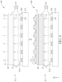
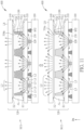
- FIG. 3 is a schematic diagram showing a cross-sectional view of a structure and lights of the light emitting device in a first state and a structure and lights of the light emitting device in a second state according to the first embodiment of the present disclosure
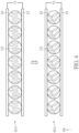
- FIG. 4 is a schematic diagram showing a light controller in a first state and a light controller in a second state according to the first embodiment of the present disclosure, wherein the first conductive line and the second conductive line are omitted in FIG. 3 to make FIG. 3 clear. Note that FIG.
- FIG. 3 uses different shadings to show the switchable diffusers 132 in different states, wherein the switchable diffusers 132 in a first state SU1 are shown by sparsely dotted shading, and the switchable diffusers 132 in a second state SU2 are shown by densely dotted shading.
- FIG. 4 only shows the first control electrode E1, the second control electrode E2 and the switchable diffusers 132 to make FIG. 4 clear. As shown in FIG.
- the light controller 130 may be switched between the first state SU1 and the second state SU2 according to the control signals received by the first control electrode E1 and the second control electrode E2, wherein the light controller 130 may collimate the lights generated by the light emitting elements 120 in the first state SU1, and the light controller 130 may diffuse the lights generated by the light emitting elements 120 in the second state SU2.
- the collimation and the diffusion of the lights may be confirmed by measuring output lights passing through the illuminating surface LS (the lights generated by the light emitting elements 120 are referred as the output lights after passing through the illuminating surface LS).
- the collimated lights mean that the sum of the intensity of the output lights of which the angle with the illuminating surface LS ranges from 80° to 100° is greater than or equal to 80% of the total intensity of the output lights. That is to say, when the sum of the intensity of the output lights of which the angle with the normal direction of the illuminating surface LS ranges from -10° to +10° is greater than or equal to 80% of the sum of the intensity of the output lights with all angles (i.e., the angle with the normal direction of the illuminating surface LS ranges from -90° to +90°), the output lights are collimated.
- the diffused lights mean that the intensity of the output lights within the observable viewing angle of the light emitting device 100 has only a small difference without rapid changes (i.e., the output lights are substantially uniformly scattered within the observable viewing angle of the light emitting device 100, and there is no area has concentrated output lights).
- the sum of the intensity of the output lights of which the angle with the illuminating surface LS ranges from 80° to 100° may be less than 80% of the total intensity of the output lights.
- the emitted directions of the lights generated by the light emitting elements 120 may be various and direct to the illuminating surface LS.
- the emitted directions of these lights in the light controller 130 may be adjusted and/or filtered by the light controller 130.
- a portion of the lights i.e., the lights L1 of which the angle with the normal direction Dn is greater
- another portion of the lights may enter the switchable diffuser 132 to be adjusted and/or filtered.
- the switchable diffusers 132 may not adjust the emitted directions (in the light controller 130) of the lights generated by the light emitting elements 120 (e.g., the switchable diffusers 132 are almost transparent). Therefore, when the lights generated by the light emitting elements 120 enter the switchable diffusers 132 in the first state SU1, the lights (e.g., the lights L2) of which the angle with the normal direction Dn is greater may be blocked by the side walls 134a of the light shielding elements 134, such that the lights may be collimated and pass through the illuminating surface LS (e.g., the lights L3).
- the lights e.g., the lights L2 of which the angle with the normal direction Dn is greater
- the switchable diffusers 132 may adjust the emitted directions (in the light controller 130) of the lights generated by the light emitting elements 120 (e.g., the switchable diffusers 132 may make the lights be diffused), and therefore, the lights may be uniformly diffused and pass through the illuminating surface LS (e.g., the lights L4). Accordingly, it can be known that, in the first state SU1 of this embodiment, the light controller 130 may collimate the lights by the light shielding elements 134; in the second state SU2 of this embodiment, the light controller 130 may diffuse the lights by the switchable diffusers 132.
- the switchable diffuser 132 may have a first haze in the first state SU1, and the switchable diffuser 132 may have a second haze in the second state SU2.
- the haze of the object described in the present disclosure represents that the percentage of the intensity of the transmitted lights which deviate from their incident lights by more than 2.5° to the total intensity of the transmitted light.
- the first haze may be less than 10, and/or the second haze may be greater than 90, but not limited thereto. As shown in FIG.
- the light emitting device 100 may provide an alternating current (AC) control signal with a first voltage difference V1 for the first control electrode E1 and the second control electrode E2 in the first state SU1, and the light emitting device 100 may provide an alternating current control signal with a second voltage difference V2 for the first control electrode E1 and the second control electrode E2 in the second state SU2, wherein the voltage difference of the alternating current control signal represents the maximum voltage difference between the signals of the two electrodes at the same time.
- AC alternating current
- the absolute value of the first voltage difference V1 may be greater than the absolute value of the second voltage difference V2, and/or the second voltage difference V2 may be close to 0, but not limited thereto. In some embodiments, the absolute value of the first voltage difference V1 may be less than the absolute value of the second voltage difference V2, and/or the first voltage difference V1 may be close to 0, but not limited thereto.
- the switchable diffuser 132 may include any suitable material which can achieve the above function.
- each switchable diffuser 132 may be a polymer dispersed liquid crystal cell (PDLC), a polymer network liquid crystal cell (PNLC), other suitable material or a combination thereof.
- the polymer dispersed liquid crystal cell and the polymer network liquid crystal cell may be respectively mixed with different polymer materials to form different crosslink structures.
- the thickness of the liquid crystal layer in the polymer network liquid crystal cell is thinner and needs the alignment layer(s); then, since the polymer network liquid crystal cell can be driven by the lower driving voltage, it can save the power. Since the liquid crystal layer in the polymer dispersed liquid crystal cell does not need the alignment layer, its manufacturing cost is lower.
- the molecules in the switchable diffuser 132 may have different arrangements in the first state SU1 and the second state SU2.
- the molecules in the switchable diffuser 132 may be substantially parallel to each other in the first state SU1 (the molecules have the similar tilt angle), and the molecules in the switchable diffusers 132 may not have the similar tilt angle in the second state SU2, but not limited thereto.
- the switchable diffuser 132 may use other type medium based on requirement(s).
- the forming methods of the light controller 130, the first control electrode E1 and the second control electrode E2 are not particularly limited.
- the first control electrode E1 and the second control electrode E2 may be respectively formed on the insulating layer 150 and the second substrate 140 by a coating process, a deposition process and/or other semiconductor process(es), and the light shielding elements 134 may be formed on the first control electrode E1 by a coating process, a deposition process and/or other semiconductor process(es).
- the first substrate 110 and the second substrate 140 may be adhered to each other by such as sealant AL, thereby assembling the first substrate 110 and the second substrate 140.
- the switchable diffusers 132 may be disposed between the first substrate 110 and the second substrate 140, so as to complete the manufacture, but not limited thereto.
- the sealant AL may be used to reduce the leakage of material in the switchable diffuser 132 in addition to assembling the first substrate 110 and the second substrate 140.
- the first control electrode E1, the light shielding element 134, the switchable diffuser 132 and the second control electrode E2 may be disposed on the insulating layer 150 in sequence, but not limited thereto.
- the light emitting device 100 of the present disclosure may be thinner, and/or the light emitting device 100 of the present disclosure may have the simplified structure.
- each light emitting element 120 may be a self-luminous type component, and each light emitting element 120 may generate the light with the intensity corresponding to the gray level signal of the image, the light emitting device 100 may be thinner even and/or may have the more simplified structure.
- the light emitting device 100 may further include other suitable component(s) and/or structure(s) based requirement(s).
- the light emitting device 100 may optionally include an optical layer, such as a polarizer and/or an anti-reflection film, disposed at any suitable position, but not limited thereto.
- the light emitting device 100 may optionally include an electrically controlled birefringence (ECB) component disposed on the light controller 130.
- EBC electrically controlled birefringence
- the electrically controlled birefringence component may be configured to decrease lateral light leakage. Therefore, the electrically controlled birefringence component may make the lights generated by the light emitting device 100 in the first state SU1 have higher light collimation.
- the light emitting device 100 has the electrically controlled birefringence component, in the lights generated by the light emitting device 100 in the first state SU1, the sum of the intensity of the output lights of which the angle with the illuminating surface LS ranges from 80° to 100° may be enhanced (e.g., this sum may be greater than or equal to 90% of the total intensity of the output lights), but not limited thereto.
- the light emitting device of the present disclosure is not limited to the above embodiments. Further embodiments of the present disclosure are described below. For ease of comparison, same components will be labeled with the same symbol in the following. The following descriptions relate the differences between each of the embodiments, and repeated parts will not be redundantly described.
- FIG. 5 is a schematic diagram showing a top view of a light emitting device according to a second embodiment of the present disclosure
- FIG. 6 is a schematic diagram showing a cross-sectional view of the light emitting device taken along a cross-sectional line B-B' in FIG. 5
- FIG. 7 is a schematic diagram showing a cross-sectional view of the light emitting device taken along a cross-sectional line C-C' in FIG. 5
- FIG. 5 only shows nine light emitting elements 120 as an example, but the light emitting device 200 may include fewer or more light emitting elements 120 in fact.
- the first conductive line and the second conductive line are omitted in FIG. 5 to FIG.
- the light emitting device 200 of this embodiment may further include a plurality of first spacers SP1, and the first spacer SP1 is disposed between the light shielding element 134 and the second control electrode E2.
- the first spacer SP1 is in contact with the light shielding element 134 and the second control electrode E2 simultaneously, but not limited thereto.
- the arrangement of the first spacers SP1 in top view, the number of the first spacers SP1 and the density of the first spacers SP1 may be adjusted based on requirement(s). For example, in FIG.
- the first spacer SP1 may be disposed at a geometric center of a smallest region containing some light emitting elements 120 ( FIG. 5 may be disposed at the geometric center of the smallest rectangle containing four light emitting elements 120), but not limited thereto.
- the shape of the aforementioned smallest region may be triangle, rectangle, polygon, circle, ellipse or other suitable shape.
- the material of the first spacer SP1 may include any suitable material, such as photoresist, resin or ink, but not limited thereto.
- FIG. 5 may be disposed at the geometric center of the smallest rectangle containing four light emitting elements 120
- the light controller 130 may further include a diffuser connecting part 132c disposed in the gap between the light shielding elements 134 and the second control electrode E2, so as to be connected to two adjacent switchable diffusers 132, wherein the material of the diffuser connecting part 132c may be the same as the material of the switchable diffusers 132.
- FIG. 8 is a schematic diagram showing a cross-sectional view of a light emitting device according to a third embodiment of the present disclosure, wherein the first conductive line and the second conductive line are omitted in FIG. 8 to make FIG. 8 clear.
- the light emitting device 300 of this embodiment further includes the third substrate 310.
- the light controller 130, the first control electrode E1 and the second control electrode E2 may be disposed between the second substrate 140 and the third substrate 310, wherein the sealant AL is configured to adhere to the second substrate 140 and the third substrate 310.
- the formation of the structures and components e.g., the light controller 130, the first control electrode E1, the second control electrode E2 and the sealant AL, etc.
- the light controlling board 320 is disposed on the light emitting elements 120 and the insulating layer 150, so as to complete the manufacture of the light emitting device 300.
- the circuit configured to provide the control signal may be disposed between the second substrate 140 and the third substrate 310, disposed between the first substrate 110 and the third substrate 310 or disposed at other suitable position based on requirement(s), and this circuit may be electrically connected to the first control electrode E1 and the second control electrode E2 through the peripheral traces PT.
- the third substrate 310 may include glass, quartz, sapphire, polyimide (PI), polyethylene terephthalate (PET), other suitable material or a combination thereof, so as to be a rigid substrate or a flexible substrate.
- the light emitting device 300 may optionally include a second spacer SP2 disposed on the first substrate 110, wherein the top of the second spacer SP2 may be higher than the light emitting element 120.
- the insulating layer 150 may cover the top of the second spacer SP2, or the top of the second spacer SP2 is higher than or equal to the top surface of the insulating layer 150. For instance, in FIG.
- the second spacer SP2 may be in contact with the third substrate 310, but not limited thereto.
- the second spacer SP2 may include any suitable material, such as photoresist, resin or ink, but not limited thereto.
- the lights having a larger angle with the normal direction Dn may be blocked, thereby making the lights emitted by the light emitting elements 120 more concentrated.
- each switchable diffuser 132 may be corresponding to (or overlapped with) one or more of the light emitting elements 120 in the normal direction Dn.
- each switchable diffuser 132 shown in FIG. 8 may be corresponding to (or overlapped with) three light emitting elements 120 in the normal direction Dn, and these three light emitting elements 120 may emit the lights with the same color or different colors.
- each switchable diffuser 132 may be corresponding to (or overlapped with) three light emitting elements 120 respectively emitting red light, green light and blue light in the normal direction Dn, but not limited thereto.
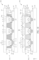
- FIG. 9 is a schematic diagram showing a cross-sectional view of a structure and lights of a light emitting device in a first state and a structure and lights of a light emitting device in a second state according to a fourth embodiment of the present disclosure, wherein the first conductive line and the second conductive line are omitted in FIG. 9 to make FIG. 9 clear.
- FIG. 9 uses different shadings to show the switchable diffusers 132 in different states, wherein the switchable diffusers 132 in the first state SU1 are shown by sparsely dotted shading, and the switchable diffusers 132 in the second state SU2 are shown by densely dotted shading. As shown in FIG.
- the light controller 130 may include two layers, one of the layers is a collimator 410, and the other layer is the switchable diffuser(s) 132 disposed on the collimator 410.
- the collimator 410 may include a plurality of collimating units 410u, and each collimating unit 410u may be corresponding to one or more of the light emitting elements 120 and configured to make the lights generated by the corresponding light emitting element(s) 120 be collimated, thereby forming the collimated lights Ld.
- switchable diffuser 132 may be similar to the first embodiment, wherein the switchable diffuser 132 may be controlled based on the control signals received by the first control electrode E1 and the second control electrode E2, such that the light controller 130 may be switchable in the first state SU1 and the second state SU2.
- the switchable diffusers 132 may not adjust the emitted directions (in the light controller 130) of the collimated lights Ld (e.g., the switchable diffuser 132 is almost transparent). Therefore, when the collimated lights Ld enter the switchable diffuser 132 in the first state SU1, the collimated lights Ld may directly pass through the illuminating surface LS (e.g., the lights L3).
- the switchable diffusers 132 may adjust the emitted directions (in the light controller 130) of the collimated lights Ld (e.g., the switchable diffuser 132 may make the lights be diffused), and therefore, the illuminating surface LS may emit uniformly diffused lights (e.g., the lights L4). Accordingly, it can be known that, the light controller 130 may adjust the collimated lights Ld to make the collimated lights Ld be diffused by the switchable diffuser 132 in the second state SU2. Note that, in FIG. 9 , the illuminating surface LS may be an outer surface of the second control electrode E2 or an outer surface of other layer disposed on the switchable diffuser 132.
- the collimator 410 and the switchable diffuser 132 are spaced apart from each other by a distance D in the normal direction Dn, and this distance D may not be greater than 0.35 mm, but not limited thereto. Owing to the existence of this distance D, the switchable diffuser 132 of the light controller 130 makes the collimated lights Ld be diffused more uniformly.
- a space between the collimator 410 and the switchable diffuser 132 may be filled with any suitable transparent material, wherein the transparent material may include such as acrylic resin, epoxy resin and/or silicon resin, but not limited thereto.
- FIG. 10 is a schematic diagram showing a cross-sectional view of a structure and lights of a light emitting device in a first state and a structure and lights of a light emitting device in a second state according to a fifth embodiment of the present disclosure, wherein the first conductive line and the second conductive line are omitted in FIG. 10 to make FIG. 10 clear.
- a difference between this embodiment and the first embodiment is the design of the light controller 130 of the light emitting device 500 of this embodiment.
- the light controller 130 of this embodiment include a plurality of the units 532 and a plurality of walls 534, wherein the disposed positions of the units 532 may be similar to the switchable diffusers of the first embodiment, the walls 534 may be similar to the light shielding elements of the above embodiment, and the disposed positions of the walls 534 may be similar to the disposed positions of the light shielding elements of the above embodiment. Accordingly, each of the units 532 may be corresponding to (or overlapped with) at least one of the light emitting elements 120 in the normal direction Dn, the walls 534 may be disposed between two adjacent units 532, and the walls 534 may not be corresponding to (or not overlapped with) the light emitting element 120 in the normal direction Dn. For instance, in FIG.
- one of the units 532 may be corresponding to (or overlapped with) one light emitting element 120 in the normal direction Dn, but not limited thereto.
- the disposed positions of the units 532 and the walls 534 of the light controller 130 may be designed based on requirement(s). For example, in some embodiments (as shown in FIG. 10 ), the wall(s) 534 may surround one unit 532 in top view, and/or two adjacent units 532 may be completely separated by the wall(s) 534, but not limited thereto.
- an angle ⁇ between a side wall 534a of the wall 534 and the illuminating surface LS may be greater than or equal to 80°, for example, but not limited thereto.
- the side wall 534a may substantially extend along an extending direction and may not be a flatten surface, and the angle ⁇ may be between this extending direction and the illuminating surface LS.
- the units 532 of the light controller 130 may be transparent (or almost transparent), such that the lights generated by the light emitting elements 120 may pass through these units 532.
- the walls 534 may be controlled based on the control signals received by the first control electrode E1 and the second control electrode E2, such that the light controller 130 may be switchable in the first state SU1 and the second state SU2, wherein the light controller 130 may collimate the lights generated by the light emitting elements 120 in the first state SU1 and may diffuse the lights generated by the light emitting elements 120 in the second state SU2.
- the walls 534 when the light controller 130 is in the first state SU1, the walls 534 may be in a non-transmissive state; when the light controller 130 is in the second state SU2, the walls 534 may be in a transmissive state. Namely, the walls 534 may be switchable in states of the transmissive state and the non-transmissive state.
- the first control electrode E1 and the second control electrode E2 may be disposed adjacent to the walls 534 of the light controller 130 at least, and the light emitting device 500 may be switchable in the first state SU1 and the second state SU2 by providing different control signals for the first control electrode E1 and the second control electrode E2. Note that FIG.
- the 10 uses different shadings to show the walls 534 in different states, wherein the walls 534 in the non-transmissive state (the light controller 130 is in the first state SU1) are shown by the shading with grids, and the walls 534 in the transmissive state (the light controller 130 is in the second state SU2) are shown by the shading with non-continuous tilt lines.
- the walls 534 are in the non-transmissive state. Hence, before the lights generated by the light emitting elements 120 enter the light controller 130, a portion of the lights (i.e., the lights L1 of which the angle with the normal direction Dn is greater) may be blocked by the bottom surface of the walls 534, and another portion of the lights may enter the units 532 which are transparent, thereby filtering the lights.
- the units 532 may not adjust the emitted directions of the lights generated by the light emitting elements 120, and the walls 534 are in the non-transmissive state, when the lights generated by the light emitting elements 120 enter the unit 532, the lights (e.g., the lights L2) of which the angle with the normal direction Dn is greater may be blocked by the side walls 534a of the walls 534 in the non-transmissive state, such that the lights may be collimated and pass through the illuminating surface LS (e.g., the lights L3).
- the walls 534 are in the transmissive state (e.g., the walls 534 are transparent or almost transparent).
- the emitted directions of the lights generated by the light emitting elements 120 may not be adjusted and/or filtered by the light controller 130 substantially.
- the lights may be diffused and pass through the illuminating surface LS (e.g., the lights L4).
- the light controller 130 may collimate the lights by the walls 534; in the second state SU2 of this embodiment, the light controller 130 may not adjust and/or filter the lights generated by the light emitting elements 120 substantially, so as to make the lights diffused.
- the wall 534 and the units 532 may individually include any suitable material which can achieve the above function.
- the refractive index of the unit 532 may range such as from 1.4 to 1.9, but not limited thereto.
- the unit 532 may include acrylic resin, polycarbonate resin, silicon resin, epoxy resin, other suitable transparent material or a combination thereof, but not limited thereto.
- the wall 534 may be made of an electrochromic material or suspend particles, but not limited thereto.
- the forming methods of the light controller 130, the first control electrode E1 and the second control electrode E2 are not particularly limited.
- the first control electrode E1 and the second control electrode E2 may be respectively formed on the insulating layer 150 and the second substrate 140 by a coating process, a deposition process and/or other semiconductor process(es), and the walls 534 and the units 532 may be formed on the first control electrode E1 or the second control electrode E2. Then, the first substrate 110 and the second substrate 140 may be adhered to each other by such as the sealant AL, thereby assembling the first substrate 110 and the second substrate 140 to complete the manufacture, but not limited thereto.
- FIG. 11 is a schematic diagram showing a cross-sectional view of a structure and lights of a light emitting device in a first state and a structure and lights of a light emitting device in a second state according to a sixth embodiment of the present disclosure, wherein the first conductive line and the second conductive line are omitted in FIG. 11 to make FIG. 11 clear.
- FIG. 11 uses different shadings to show the walls 534 in different states, wherein the walls 534 in the first state SU1 are shown by the shading with grids, and the walls 534 in the second state SU2 are shown by the shading with non-continuous tilt lines. As shown in FIG.
- the light emitting device 600 of this embodiment further includes a third substrate 310.
- the light controller 130, the first control electrode E1 and the second control electrode E2 are disposed between the second substrate 140 and the third substrate 310, wherein the sealant AL is configured to adhere to the second substrate 140 and the third substrate 310, such that the second substrate 140, the third substrate 310 and the structures and components therebetween form a light controlling board 320.
- the details of the third substrate 310 and the light controlling board 320 may be referred to the third embodiment of the present disclosure, and these will not be redundantly described.
- the light emitting device 600 may optionally include a second spacer SP2 disposed on the first substrate 110, wherein the top of the second spacer SP2 is higher than the light emitting elements 120.
- the details of the second spacer SP2 may be referred to the third embodiment of the present disclosure, and these will not be redundantly described.
- the lights e.g., the lights L5 having a larger angle with the normal direction Dn may be blocked, thereby making the lights emitted by the light emitting elements 120 more concentrated.
- the light controller 130 may further include an unit connecting part 532c disposed in the gap between the walls 534 and the second control electrode E2, so as to be connected to two adjacent units 532, wherein the material of the unit connecting part 532c may be the same as the material of the units 532.
- the light emitting device may further include a first spacer disposed between the wall 534 and the second control electrode E2, so as to generate the above gap. The details of the first spacer may be referred to the second embodiment of the present disclosure, and these will not be redundantly described.
- the light emitting device of the present disclosure may control or adjust the light direction emitted from the illuminating surface by the light controller, thereby enhancing the privacy of viewing and/or preventing specific persons from viewing. Furthermore, compared with the traditional electronic device with the function of controlling the light direction, the light emitting device of the present disclosure may be thinner, and/or the light emitting device of the present disclosure may have the simplified structure.
Landscapes
- Physics & Mathematics (AREA)
- Nonlinear Science (AREA)
- Chemical & Material Sciences (AREA)
- Crystallography & Structural Chemistry (AREA)
- General Physics & Mathematics (AREA)
- Optics & Photonics (AREA)
- Mathematical Physics (AREA)
- Dispersion Chemistry (AREA)
- Engineering & Computer Science (AREA)
- General Engineering & Computer Science (AREA)
- Electroluminescent Light Sources (AREA)
- Led Device Packages (AREA)
Applications Claiming Priority (2)
| Application Number | Priority Date | Filing Date | Title |
|---|---|---|---|
| CN202010338925.2A CN113555490A (zh) | 2020-04-26 | 2020-04-26 | 发光装置 |
| EP21165893.5A EP3901695A1 (de) | 2020-04-26 | 2021-03-30 | Lichtemittierende vorrichtung |
Related Parent Applications (1)
| Application Number | Title | Priority Date | Filing Date |
|---|---|---|---|
| EP21165893.5A Division EP3901695A1 (de) | 2020-04-26 | 2021-03-30 | Lichtemittierende vorrichtung |
Publications (3)
| Publication Number | Publication Date |
|---|---|
| EP4293418A2 true EP4293418A2 (de) | 2023-12-20 |
| EP4293418A3 EP4293418A3 (de) | 2024-03-20 |
| EP4293418B1 EP4293418B1 (de) | 2026-05-06 |
Family
ID=75302316
Family Applications (2)
| Application Number | Title | Priority Date | Filing Date |
|---|---|---|---|
| EP23206572.2A Active EP4293418B1 (de) | 2020-04-26 | 2021-03-30 | Lichtemittierende vorrichtung |
| EP21165893.5A Withdrawn EP3901695A1 (de) | 2020-04-26 | 2021-03-30 | Lichtemittierende vorrichtung |
Family Applications After (1)
| Application Number | Title | Priority Date | Filing Date |
|---|---|---|---|
| EP21165893.5A Withdrawn EP3901695A1 (de) | 2020-04-26 | 2021-03-30 | Lichtemittierende vorrichtung |
Country Status (3)
| Country | Link |
|---|---|
| US (3) | US11221126B2 (de) |
| EP (2) | EP4293418B1 (de) |
| CN (2) | CN113555490A (de) |
Families Citing this family (2)
| Publication number | Priority date | Publication date | Assignee | Title |
|---|---|---|---|---|
| JP7388902B2 (ja) * | 2019-12-10 | 2023-11-29 | 株式会社ジャパンディスプレイ | 表示装置 |
| CN114822273B (zh) * | 2022-05-07 | 2022-12-23 | Tcl华星光电技术有限公司 | 拼接面板 |
Citations (1)
| Publication number | Priority date | Publication date | Assignee | Title |
|---|---|---|---|---|
| CN110568653A (zh) * | 2019-09-12 | 2019-12-13 | 武汉华星光电技术有限公司 | 显示面板及显示装置 |
Family Cites Families (10)
| Publication number | Priority date | Publication date | Assignee | Title |
|---|---|---|---|---|
| US8427605B2 (en) * | 2008-09-23 | 2013-04-23 | Koninklijke Philips Electronics N.V. | Illumination device with electrical variable scattering element |
| DE202009016729U1 (de) * | 2009-12-09 | 2011-04-28 | Heise, Sebastian, Dipl.-Ing. (FH) | Beleuchtungseinrichtung mit mindestens einer LED |
| KR20130045687A (ko) * | 2011-10-26 | 2013-05-06 | 엘지이노텍 주식회사 | 발광 장치 및 이를 구비한 조명 장치 |
| US9841167B2 (en) * | 2014-09-25 | 2017-12-12 | GE Lighting Solutions, LLC | Lighting system with actively controllable optics and method |
| US9816687B2 (en) * | 2015-09-24 | 2017-11-14 | Intel Corporation | MEMS LED zoom |
| TWI605287B (zh) * | 2016-12-29 | 2017-11-11 | 揚昇照明股份有限公司 | 顯示裝置 |
| CN106597727A (zh) * | 2017-01-11 | 2017-04-26 | 北京大学 | 一种透射光角度范围可调控的电控调光膜 |
| JP7083102B2 (ja) * | 2017-11-29 | 2022-06-10 | Tianma Japan株式会社 | 光線方向制御デバイス及び表示装置 |
| US10894511B2 (en) * | 2018-02-27 | 2021-01-19 | Ford Global Technologies, Llc | Vehicle window assembly having a light-producing assembly |
| US12066165B2 (en) * | 2020-04-26 | 2024-08-20 | Innolux Corporation | Light emitting device |
-
2020
- 2020-04-26 CN CN202010338925.2A patent/CN113555490A/zh active Pending
- 2020-04-26 CN CN202311189286.8A patent/CN117199219A/zh active Pending
-
2021
- 2021-03-26 US US17/213,239 patent/US11221126B2/en active Active
- 2021-03-30 EP EP23206572.2A patent/EP4293418B1/de active Active
- 2021-03-30 EP EP21165893.5A patent/EP3901695A1/de not_active Withdrawn
- 2021-12-13 US US17/548,596 patent/US12018816B2/en active Active
-
2024
- 2024-05-15 US US18/664,311 patent/US12253237B2/en active Active
Patent Citations (2)
| Publication number | Priority date | Publication date | Assignee | Title |
|---|---|---|---|---|
| CN110568653A (zh) * | 2019-09-12 | 2019-12-13 | 武汉华星光电技术有限公司 | 显示面板及显示装置 |
| US20210080779A1 (en) * | 2019-09-12 | 2021-03-18 | Wuhan China Star Optoelectronics Technology Co., Ltd. | Display Panel and Display Device |
Also Published As
| Publication number | Publication date |
|---|---|
| US11221126B2 (en) | 2022-01-11 |
| CN113555490A (zh) | 2021-10-26 |
| EP4293418B1 (de) | 2026-05-06 |
| US20220099275A1 (en) | 2022-03-31 |
| US20240302027A1 (en) | 2024-09-12 |
| CN117199219A (zh) | 2023-12-08 |
| US20210332967A1 (en) | 2021-10-28 |
| US12253237B2 (en) | 2025-03-18 |
| EP3901695A1 (de) | 2021-10-27 |
| EP4293418A3 (de) | 2024-03-20 |
| US12018816B2 (en) | 2024-06-25 |
Similar Documents
| Publication | Publication Date | Title |
|---|---|---|
| US12247720B2 (en) | Light emitting device | |
| US9519186B2 (en) | Display device including a color conversion layer | |
| US9575228B2 (en) | Display device including a color conversion layer | |
| US12253237B2 (en) | Light emitting device | |
| US11947131B2 (en) | Display device | |
| US9857642B2 (en) | Display device and liquid crystal display device | |
| KR20210047499A (ko) | 가변 차광 블랙 매트릭스층을 구비하는 표시 장치 | |
| US12353075B2 (en) | Electronic device | |
| CN217718925U (zh) | 显示装置 | |
| US20250130423A1 (en) | Head-up display system and vehicle system | |
| US9664942B2 (en) | Liquid crystal display | |
| CN113284411B (zh) | 电子装置 | |
| EP4020579A1 (de) | Farbumwandlungssubstrat, anzeigevorrichtung und verfahren zur herstellung eines farbumwandlungssubstrats | |
| US12358426B2 (en) | Light emitting device | |
| US20260063951A1 (en) | Reflective electronic device and preparation method thereof | |
| TWM650976U (zh) | 顯示裝置 | |
| CN116723724A (zh) | 电子装置 |
Legal Events
| Date | Code | Title | Description |
|---|---|---|---|
| PUAI | Public reference made under article 153(3) epc to a published international application that has entered the european phase |
Free format text: ORIGINAL CODE: 0009012 |
|
| STAA | Information on the status of an ep patent application or granted ep patent |
Free format text: STATUS: THE APPLICATION HAS BEEN PUBLISHED |
|
| AC | Divisional application: reference to earlier application |
Ref document number: 3901695 Country of ref document: EP Kind code of ref document: P |
|
| AK | Designated contracting states |
Kind code of ref document: A2 Designated state(s): AL AT BE BG CH CY CZ DE DK EE ES FI FR GB GR HR HU IE IS IT LI LT LU LV MC MK MT NL NO PL PT RO RS SE SI SK SM TR |
|
| REG | Reference to a national code |
Ref country code: DE Ref legal event code: R079 Free format text: PREVIOUS MAIN CLASS: G02F0001133500 Ipc: G02F0001133400 Ref country code: DE Ref legal event code: R079 Ref document number: 602021054186 Country of ref document: DE Free format text: PREVIOUS MAIN CLASS: G02F0001133500 Ipc: G02F0001133400 |
|
| PUAL | Search report despatched |
Free format text: ORIGINAL CODE: 0009013 |
|
| AK | Designated contracting states |
Kind code of ref document: A3 Designated state(s): AL AT BE BG CH CY CZ DE DK EE ES FI FR GB GR HR HU IE IS IT LI LT LU LV MC MK MT NL NO PL PT RO RS SE SI SK SM TR |
|
| RIC1 | Information provided on ipc code assigned before grant |
Ipc: G02F 1/13 20060101ALI20240209BHEP Ipc: G02F 1/1335 20060101ALI20240209BHEP Ipc: G02F 1/1334 20060101AFI20240209BHEP |
|
| STAA | Information on the status of an ep patent application or granted ep patent |
Free format text: STATUS: REQUEST FOR EXAMINATION WAS MADE |
|
| 17P | Request for examination filed |
Effective date: 20240917 |
|
| RBV | Designated contracting states (corrected) |
Designated state(s): AL AT BE BG CH CY CZ DE DK EE ES FI FR GB GR HR HU IE IS IT LI LT LU LV MC MK MT NL NO PL PT RO RS SE SI SK SM TR |
|
| GRAP | Despatch of communication of intention to grant a patent |
Free format text: ORIGINAL CODE: EPIDOSNIGR1 |
|
| STAA | Information on the status of an ep patent application or granted ep patent |
Free format text: STATUS: GRANT OF PATENT IS INTENDED |
|
| INTG | Intention to grant announced |
Effective date: 20260112 |
|
| GRAS | Grant fee paid |
Free format text: ORIGINAL CODE: EPIDOSNIGR3 |
|
| GRAA | (expected) grant |
Free format text: ORIGINAL CODE: 0009210 |
|
| STAA | Information on the status of an ep patent application or granted ep patent |
Free format text: STATUS: THE PATENT HAS BEEN GRANTED |