EP4290748A1 - Voltage regulator with reduced power loss and chip using the voltage regulator - Google Patents
Voltage regulator with reduced power loss and chip using the voltage regulator Download PDFInfo
- Publication number
- EP4290748A1 EP4290748A1 EP23174119.0A EP23174119A EP4290748A1 EP 4290748 A1 EP4290748 A1 EP 4290748A1 EP 23174119 A EP23174119 A EP 23174119A EP 4290748 A1 EP4290748 A1 EP 4290748A1
- Authority
- EP
- European Patent Office
- Prior art keywords
- terminal
- energy storage
- storage element
- voltage
- voltage regulator
- Prior art date
- Legal status (The legal status is an assumption and is not a legal conclusion. Google has not performed a legal analysis and makes no representation as to the accuracy of the status listed.)
- Withdrawn
Links
- 238000004146 energy storage Methods 0.000 claims abstract description 87
- 239000003990 capacitor Substances 0.000 claims description 11
- 238000007599 discharging Methods 0.000 claims description 4
- 230000008878 coupling Effects 0.000 claims 5
- 238000010168 coupling process Methods 0.000 claims 5
- 238000005859 coupling reaction Methods 0.000 claims 5
- 238000012986 modification Methods 0.000 description 4
- 230000004048 modification Effects 0.000 description 4
- 230000001105 regulatory effect Effects 0.000 description 4
- 238000010586 diagram Methods 0.000 description 2
- 230000001276 controlling effect Effects 0.000 description 1
- 238000007796 conventional method Methods 0.000 description 1
- 238000005516 engineering process Methods 0.000 description 1
Images

Classifications
-
- H—ELECTRICITY
- H02—GENERATION; CONVERSION OR DISTRIBUTION OF ELECTRIC POWER
- H02M—APPARATUS FOR CONVERSION BETWEEN AC AND AC, BETWEEN AC AND DC, OR BETWEEN DC AND DC, AND FOR USE WITH MAINS OR SIMILAR POWER SUPPLY SYSTEMS; CONVERSION OF DC OR AC INPUT POWER INTO SURGE OUTPUT POWER; CONTROL OR REGULATION THEREOF
- H02M3/00—Conversion of DC power input into DC power output
- H02M3/02—Conversion of DC power input into DC power output without intermediate conversion into AC
- H02M3/04—Conversion of DC power input into DC power output without intermediate conversion into AC by static converters
- H02M3/06—Conversion of DC power input into DC power output without intermediate conversion into AC by static converters using resistors or capacitors, e.g. potential divider
- H02M3/07—Conversion of DC power input into DC power output without intermediate conversion into AC by static converters using resistors or capacitors, e.g. potential divider using capacitors charged and discharged alternately by semiconductor devices with control electrode, e.g. charge pumps
-
- H—ELECTRICITY
- H02—GENERATION; CONVERSION OR DISTRIBUTION OF ELECTRIC POWER
- H02M—APPARATUS FOR CONVERSION BETWEEN AC AND AC, BETWEEN AC AND DC, OR BETWEEN DC AND DC, AND FOR USE WITH MAINS OR SIMILAR POWER SUPPLY SYSTEMS; CONVERSION OF DC OR AC INPUT POWER INTO SURGE OUTPUT POWER; CONTROL OR REGULATION THEREOF
- H02M1/00—Details of apparatus for conversion
- H02M1/0095—Hybrid converter topologies, e.g. NPC mixed with flying capacitor, thyristor converter mixed with MMC or charge pump mixed with buck
-
- H—ELECTRICITY
- H02—GENERATION; CONVERSION OR DISTRIBUTION OF ELECTRIC POWER
- H02M—APPARATUS FOR CONVERSION BETWEEN AC AND AC, BETWEEN AC AND DC, OR BETWEEN DC AND DC, AND FOR USE WITH MAINS OR SIMILAR POWER SUPPLY SYSTEMS; CONVERSION OF DC OR AC INPUT POWER INTO SURGE OUTPUT POWER; CONTROL OR REGULATION THEREOF
- H02M1/00—Details of apparatus for conversion
- H02M1/14—Arrangements for reducing ripples from DC input or output
- H02M1/15—Arrangements for reducing ripples from DC input or output using active elements
-
- H—ELECTRICITY
- H02—GENERATION; CONVERSION OR DISTRIBUTION OF ELECTRIC POWER
- H02M—APPARATUS FOR CONVERSION BETWEEN AC AND AC, BETWEEN AC AND DC, OR BETWEEN DC AND DC, AND FOR USE WITH MAINS OR SIMILAR POWER SUPPLY SYSTEMS; CONVERSION OF DC OR AC INPUT POWER INTO SURGE OUTPUT POWER; CONTROL OR REGULATION THEREOF
- H02M3/00—Conversion of DC power input into DC power output
- H02M3/02—Conversion of DC power input into DC power output without intermediate conversion into AC
- H02M3/04—Conversion of DC power input into DC power output without intermediate conversion into AC by static converters
- H02M3/06—Conversion of DC power input into DC power output without intermediate conversion into AC by static converters using resistors or capacitors, e.g. potential divider
- H02M3/07—Conversion of DC power input into DC power output without intermediate conversion into AC by static converters using resistors or capacitors, e.g. potential divider using capacitors charged and discharged alternately by semiconductor devices with control electrode, e.g. charge pumps
- H02M3/072—Conversion of DC power input into DC power output without intermediate conversion into AC by static converters using resistors or capacitors, e.g. potential divider using capacitors charged and discharged alternately by semiconductor devices with control electrode, e.g. charge pumps adapted to generate an output voltage whose value is lower than the input voltage
-
- H—ELECTRICITY
- H02—GENERATION; CONVERSION OR DISTRIBUTION OF ELECTRIC POWER
- H02M—APPARATUS FOR CONVERSION BETWEEN AC AND AC, BETWEEN AC AND DC, OR BETWEEN DC AND DC, AND FOR USE WITH MAINS OR SIMILAR POWER SUPPLY SYSTEMS; CONVERSION OF DC OR AC INPUT POWER INTO SURGE OUTPUT POWER; CONTROL OR REGULATION THEREOF
- H02M3/00—Conversion of DC power input into DC power output
- H02M3/02—Conversion of DC power input into DC power output without intermediate conversion into AC
- H02M3/04—Conversion of DC power input into DC power output without intermediate conversion into AC by static converters
- H02M3/10—Conversion of DC power input into DC power output without intermediate conversion into AC by static converters using discharge tubes with control electrode or semiconductor devices with control electrode
- H02M3/145—Conversion of DC power input into DC power output without intermediate conversion into AC by static converters using discharge tubes with control electrode or semiconductor devices with control electrode using devices of a triode or transistor type requiring continuous application of a control signal
- H02M3/155—Conversion of DC power input into DC power output without intermediate conversion into AC by static converters using discharge tubes with control electrode or semiconductor devices with control electrode using devices of a triode or transistor type requiring continuous application of a control signal using semiconductor devices only
- H02M3/156—Conversion of DC power input into DC power output without intermediate conversion into AC by static converters using discharge tubes with control electrode or semiconductor devices with control electrode using devices of a triode or transistor type requiring continuous application of a control signal using semiconductor devices only with automatic control of output voltage or current, e.g. switching regulators
- H02M3/158—Conversion of DC power input into DC power output without intermediate conversion into AC by static converters using discharge tubes with control electrode or semiconductor devices with control electrode using devices of a triode or transistor type requiring continuous application of a control signal using semiconductor devices only with automatic control of output voltage or current, e.g. switching regulators including plural semiconductor devices as final control devices for a single load
Definitions
- the present invention relates to voltage regulators.
- ACR the ac resistance of an inductor
- a voltage regulator down converting an input voltage to an output voltage in accordance with an exemplary embodiment of the present invention has an input terminal receiving the input voltage, and an output terminal outputting the output voltage.
- the voltage regulator further has three energy storage elements.
- the first energy storage element provides a pre-charged voltage between a connection terminal and a ground terminal during a first phase.
- the second energy storage element has a first terminal, and has a second terminal coupled to the output terminal of the voltage regulator.
- the third energy storage element is coupled between the output terminal of the voltage regulator and the ground terminal.
- the first terminal of the second energy storage element is coupled to the first energy storage element through the connection terminal to receive the pre-charged voltage from the first energy storage element.
- the first energy storage element is coupled between the input terminal and the output terminal of the voltage regulator to be pre-charged to store the pre-charged voltage, and the first terminal of the second energy storage element is coupled to the ground terminal.
- the first energy storage element may include a capacitor.
- the second energy storage element may include an inductor.
- the third energy storage element may include a capacitor.
- the first energy storage element has a first terminal and a second terminal.
- the first terminal of the first energy storage element is coupled to the first terminal of the second energy storage element through the connection terminal, and the second terminal of the first energy storage element is coupled to the ground terminal.
- the first terminal of the first energy storage element is coupled to the input terminal of the voltage regulator, and the second terminal of the first energy storage element is coupled to the output terminal of the voltage regulator.
- the pre-charged voltage stored between the first terminal and the second terminal of the first energy storage element is the input voltage minus the output voltage.
- the duty cycle of the first phase is the ratio of the output voltage and the difference voltage.
- the difference voltage is the input voltage minus the output voltage.
- the second energy storage element is charged by the pre-charged voltage that is received from the first energy storage element.
- a discharge path for the second energy storage element is established and a discharging current from the first terminal of the second energy storage element to the second terminal of the second energy element is generated.
- a chip in accordance with an exemplary embodiment of the present invention has the forgoing voltage regulator and a load circuit driven by the output voltage provided by the voltage regulator.
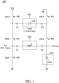
- FIG. 1 illustrates a voltage regulator 100 in accordance with an exemplary embodiment of the present invention.
- the voltage regulator 100 down converts an input voltage Vin (received by an input terminal of the voltage regulator 100) to an output voltage Vout (output through an output terminal of the voltage regulator 100).
- the voltage regulator 100 has three energy storage elements (SE1, SE2, and SE3), and five switches SW1-SW5.
- the first energy storage element SE1 includes a capacitor Cfp.
- the second energy storage element SE2 includes an inductor L.
- the third energy storage element SE3 includes a capacitor Cout. There may be modifications on any of the energy storage elements SE1, SE2, and SE3.
- the first energy storage element SE1 has a first terminal tc1 and a second terminal tc2.
- the second energy storage element SE2 has a first terminal t l 1 and a second terminal t l 2.
- the second terminal t l 2 of the second energy storage element SE2 is coupled to the output terminal (Vout) of the voltage regulator 100.
- the third energy storage element SE3 is coupled between the output terminal Vout of the voltage regulator 100 and the ground terminal.
- the energy of the input voltage Vin is transferred to the first energy storage element SE1 first, and then coupled to the second energy storage element SE2 to regulate the output voltage Vout.
- the switches SW1 to SW5 are provided to implement the energy transferring.
- the first switch SW1 and the second switch SW2 controlled by a signal ⁇ A are closed during a first phase, and may be open during a second phase.
- the third switch SW3, fourth switch SW4, and fifth switch SW5 controlled by a signal ⁇ B are closed during the second phase, and may be open during the first phase.
- the voltage regulator 100 is repeatedly switched between the first phase (e.g., enabled by ⁇ A) and the second phase (e.g., enabled by ⁇ B), and thereby generate the regulated output voltage Vout.
- the first switch SW1 couples the second terminal tc2 of the first energy storage element SE1 to a ground terminal
- the second switch SW2 couples the first terminal tc1 of the first energy storage element SE1 to the first terminal tl1 of the second energy storage element SE2 through a connection terminal txl.
- the third switch SW3 couples the input terminal Vin of the voltage regulator 100 to the first terminal tc1 of the first energy storage element SE1
- the fourth switch SW4 couples the second terminal tc2 of the first energy storage element SE1 to the output terminal Vout of the voltage regulator 100
- the fifth switch SW5 couples the first terminal t l 1 of the second energy storage element SE2 to the ground terminal.
- the second phase is a precharging phase, wherein the first energy storage element SE1 is pre-charged to store a pre-charged voltage Vpre (e.g., Vin minus Vout).
- Vpre e.g., Vin minus Vout
- the pre-charged voltage Vpre is coupled to the connection terminal tx l to be coupled to the second energy storage element SE2 that includes the inductor L.
- the voltage level at the connection terminal tx l i.e., the first terminal of the second storage element SE2
- Vpre Vin-Vout
- the voltage range supplied to drive the second storage element SE2 of the present invention is suppressed to 0V ⁇ (Vin-Vout).
- the ripple of the current through the second storage element SE2 is successfully suppressed.
- the ACR loss is suppressed.
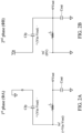
- FIG. 2A shows the circuit connection of the voltage regulator 100 during the first phase (enabled by ⁇ A).
- FIG. 2B shows the circuit connection of the voltage regulator 100 during the second phase (enabled by ⁇ B).
- the capacitor Cfp (implementing the first energy storage element SE1) is coupled between the input terminal Vin and the output terminal Vout of the voltage regulator 100 to be charged to store the pre-charged voltage (Vin-Vout), and the connection terminal tx l (at one end of the inductor L, wherein the inductor L implements the second energy storage element SE2) is coupled to the ground terminal (0V).
- the inductor L is coupled to the capacitor Cfp through the connection terminal tx l to receive the pre-charged voltage (Vin-Vout) from the capacitor Cfp.
- the inductor L is charged by the pre-charged voltage (Vin-Vout) received from the capacitor Cfp, and the connection terminal tx l (at one end of the inductor L) is changed to (Vin-Vout).
- FIG. 2A and FIG. 2B clearly show that the voltage range at the connection terminal tx l (at one end of the inductor L) is suppressed to 0V ⁇ (Vin-Vout), which is a smaller swing in comparison with a conventional voltage range 0V ⁇ Vout supplied to one end of an inductor of a conventional buck converter.
- the current ripple through the inductor L is significantly reduced.
- the ACR loss is successfully suppressed in the proposed voltage regulator.
- a regulated output voltage Vout is generated at the output terminal of the voltage regulator.
- the capacitor Cfp (the first energy storage element SE1) also shares the current loading of the voltage regulator.
- the average current through the inductor L is significantly reduced.
- the conduction loss (I 2 R) is successfully suppressed in the proposed voltage regulator.
- a duty cycle of the first phase is a ratio of the output voltage Vout to a difference voltage (Vin-Vout).
- Any voltage regulator using switches to pre-charge an energy storage element based on the input voltage Vin and transfer the pre-charged voltage from the energy storage element to an inductor L to generate the regulated output voltage Vout should be considered within the scope of the present invention.
- FIG. 3 is a block diagram illustrating a chip 300 in accordance with an exemplary embodiment of the present invention.
- the chip 300 uses the proposed voltage regulator 100 to provide the regulated output voltage Vout to drive a load circuit 302.
Landscapes
- Engineering & Computer Science (AREA)
- Power Engineering (AREA)
- Dc-Dc Converters (AREA)
- Continuous-Control Power Sources That Use Transistors (AREA)
Abstract
A down-converted voltage regulator is provided. The first energy storage element provides a pre-charged voltage between a connection terminal and a ground terminal during the first phase. The second energy storage element has a first terminal, and it has a second terminal coupled to the output terminal of the voltage regulator. The third energy storage element is coupled between the output terminal of the voltage regulator and the ground terminal. During the first phase, the first terminal of the second energy storage element is coupled to the first energy storage element through the connection terminal to receive the pre-charged voltage. During the second phase, the first energy storage element is coupled between the input terminal and the output terminal of the voltage regulator to be pre-charged to store the pre-charged voltage, and the first terminal of the second energy storage element is coupled to the ground terminal.
Description
- The present invention relates to voltage regulators.
- ACR (the ac resistance of an inductor) loss, conduction loss, switching loss, and other problems may cause excessive power consumption in a voltage regulator.
- How to reduce power loss in a voltage regulator is an important topic in this field of technology.
- A voltage regulator down converting an input voltage to an output voltage in accordance with an exemplary embodiment of the present invention has an input terminal receiving the input voltage, and an output terminal outputting the output voltage. The voltage regulator further has three energy storage elements. The first energy storage element provides a pre-charged voltage between a connection terminal and a ground terminal during a first phase. The second energy storage element has a first terminal, and has a second terminal coupled to the output terminal of the voltage regulator. The third energy storage element is coupled between the output terminal of the voltage regulator and the ground terminal. During the first phase, the first terminal of the second energy storage element is coupled to the first energy storage element through the connection terminal to receive the pre-charged voltage from the first energy storage element. During a second phase, the first energy storage element is coupled between the input terminal and the output terminal of the voltage regulator to be pre-charged to store the pre-charged voltage, and the first terminal of the second energy storage element is coupled to the ground terminal.
- The first energy storage element may include a capacitor. The second energy storage element may include an inductor. The third energy storage element may include a capacitor.
- In an exemplary embodiment, the first energy storage element has a first terminal and a second terminal. During the first phase, the first terminal of the first energy storage element is coupled to the first terminal of the second energy storage element through the connection terminal, and the second terminal of the first energy storage element is coupled to the ground terminal. During the second phase, the first terminal of the first energy storage element is coupled to the input terminal of the voltage regulator, and the second terminal of the first energy storage element is coupled to the output terminal of the voltage regulator.
- In an exemplary embodiment, the pre-charged voltage stored between the first terminal and the second terminal of the first energy storage element is the input voltage minus the output voltage.
- In an exemplary embodiment, the duty cycle of the first phase is the ratio of the output voltage and the difference voltage. The difference voltage is the input voltage minus the output voltage.
- In an exemplary embodiment, during the first phase, the second energy storage element is charged by the pre-charged voltage that is received from the first energy storage element.
- In an exemplary embodiment, during the second phase, a discharge path for the second energy storage element is established and a discharging current from the first terminal of the second energy storage element to the second terminal of the second energy element is generated.
- A chip in accordance with an exemplary embodiment of the present invention has the forgoing voltage regulator and a load circuit driven by the output voltage provided by the voltage regulator.
- A detailed description is given in the following embodiments with reference to the accompanying drawings.
- The present invention can be more fully understood by reading the subsequent detailed description and examples with references made to the accompanying drawings, wherein:
-
FIG. 1 illustrates avoltage regulator 100 in accordance with an exemplary embodiment of the present invention; -
FIG. 2A shows the circuit connection of thevoltage regulator 100 during the first phase (enabled by ΦA); -
FIG. 2B shows the circuit connection of thevoltage regulator 100 during the second phase (enabled by ΦB); and -
FIG. 3 is a block diagram illustrating achip 300 in accordance with an exemplary embodiment of the present invention. - The following description is made for the purpose of illustrating the general principles of the invention and should not be taken in a limiting sense. The scope of the invention is best determined by reference to the appended claims.
-
FIG. 1 illustrates avoltage regulator 100 in accordance with an exemplary embodiment of the present invention. Thevoltage regulator 100 down converts an input voltage Vin (received by an input terminal of the voltage regulator 100) to an output voltage Vout (output through an output terminal of the voltage regulator 100). Thevoltage regulator 100 has three energy storage elements (SE1, SE2, and SE3), and five switches SW1-SW5. - The first energy storage element SE1 includes a capacitor Cfp. The second energy storage element SE2 includes an inductor L. The third energy storage element SE3 includes a capacitor Cout. There may be modifications on any of the energy storage elements SE1, SE2, and SE3.
- The first energy storage element SE1 has a first terminal tc1 and a second terminal tc2. The second energy storage element SE2 has a first terminal tl1 and a second terminal tl2. The second terminal tl2 of the second energy storage element SE2 is coupled to the output terminal (Vout) of the
voltage regulator 100. The third energy storage element SE3 is coupled between the output terminal Vout of thevoltage regulator 100 and the ground terminal. - The energy of the input voltage Vin is transferred to the first energy storage element SE1 first, and then coupled to the second energy storage element SE2 to regulate the output voltage Vout. The switches SW1 to SW5 are provided to implement the energy transferring.
- Two phases are introduced to operate the
voltage regulator 100. - The first switch SW1 and the second switch SW2 controlled by a signal ΦA are closed during a first phase, and may be open during a second phase. The third switch SW3, fourth switch SW4, and fifth switch SW5 controlled by a signal ΦB are closed during the second phase, and may be open during the first phase. Through the signalsΦA andΦB, the
voltage regulator 100 is repeatedly switched between the first phase (e.g., enabled by ΦA) and the second phase (e.g., enabled by ΦB), and thereby generate the regulated output voltage Vout. - During the first phase (enabled by ΦA), the first switch SW1 couples the second terminal tc2 of the first energy storage element SE1 to a ground terminal, and the second switch SW2 couples the first terminal tc1 of the first energy storage element SE1 to the first terminal tl1 of the second energy storage element SE2 through a connection terminal txl.
- During the second phase (enabled by ΦB), the third switch SW3 couples the input terminal Vin of the
voltage regulator 100 to the first terminal tc1 of the first energy storage element SE1, the fourth switch SW4 couples the second terminal tc2 of the first energy storage element SE1 to the output terminal Vout of thevoltage regulator 100, and the fifth switch SW5 couples the first terminal tl1 of the second energy storage element SE2 to the ground terminal. - As for the first storage element SE1, the second phase (enabled by ΦB) is a precharging phase, wherein the first energy storage element SE1 is pre-charged to store a pre-charged voltage Vpre (e.g., Vin minus Vout). When being switched to the first phase (referring toΦA), the pre-charged voltage Vpre (e.g., Vin minus Vout) is coupled to the connection terminal txl to be coupled to the second energy storage element SE2 that includes the inductor L. By switching between the first and second phases (by controlling the signals ΦA and ΦB), the voltage level at the connection terminal txl (i.e., the first terminal of the second storage element SE2) is changed between 0V and Vpre (= Vin-Vout). In comparison with a voltage range, 0V~Vin, conventionally supplied to drive an inductor of a conventional buck converter, the voltage range supplied to drive the second storage element SE2 of the present invention is suppressed to 0V~ (Vin-Vout). Thus, the ripple of the current through the second storage element SE2 is successfully suppressed. The ACR loss is suppressed.
-
FIG. 2A shows the circuit connection of thevoltage regulator 100 during the first phase (enabled by ΦA).FIG. 2B shows the circuit connection of thevoltage regulator 100 during the second phase (enabled by ΦB). - Referring to
FIG. 2B , during the second phase (enabled byΦB), the capacitor Cfp (implementing the first energy storage element SE1) is coupled between the input terminal Vin and the output terminal Vout of thevoltage regulator 100 to be charged to store the pre-charged voltage (Vin-Vout), and the connection terminal txl (at one end of the inductor L, wherein the inductor L implements the second energy storage element SE2) is coupled to the ground terminal (0V). - Referring to
FIG. 2A , during the first phase (enabled byΦA), the inductor L is coupled to the capacitor Cfp through the connection terminal txl to receive the pre-charged voltage (Vin-Vout) from the capacitor Cfp. The inductor L is charged by the pre-charged voltage (Vin-Vout) received from the capacitor Cfp, and the connection terminal txl (at one end of the inductor L) is changed to (Vin-Vout). -
FIG. 2A and FIG. 2B clearly show that the voltage range at the connection terminal txl (at one end of the inductor L) is suppressed to 0V~ (Vin-Vout), which is a smaller swing in comparison with aconventional voltage range 0V~Vout supplied to one end of an inductor of a conventional buck converter. The current ripple through the inductor L is significantly reduced. The ACR loss is successfully suppressed in the proposed voltage regulator. - By switching the voltage regulator between the first phase (enabled by ΦA) and the second phase (enabled byΦB), a regulated output voltage Vout is generated at the output terminal of the voltage regulator.
- Note that during the second phase (enabled byΦB) wherein a discharge path for the inductor L (the second energy storage element) is established (a discharging current from tl1 to tl2), the capacitor Cfp (the first energy storage element SE1) also shares the current loading of the voltage regulator. Thus, in comparison with the conventional techniques, the average current through the inductor L is significantly reduced. The conduction loss (I2R) is successfully suppressed in the proposed voltage regulator.
- A duty cycle of the first phase (enabled byΦA) is a ratio of the output voltage Vout to a difference voltage (Vin-Vout).
- There may be other circuit modifications on the proposed voltage regulator. Any voltage regulator using switches to pre-charge an energy storage element based on the input voltage Vin and transfer the pre-charged voltage from the energy storage element to an inductor L to generate the regulated output voltage Vout should be considered within the scope of the present invention.
-
FIG. 3 is a block diagram illustrating achip 300 in accordance with an exemplary embodiment of the present invention. Thechip 300 uses the proposedvoltage regulator 100 to provide the regulated output voltage Vout to drive aload circuit 302. - Any chip using the voltage regular of the present invention should be considered within the scope of the present invention.
- While the invention has been described by way of example and in terms of the preferred embodiments, it should be understood that the invention is not limited to the disclosed embodiments. On the contrary, it is intended to cover various modifications and similar arrangements (as would be apparent to those skilled in the art). Therefore, the scope of the appended claims should be accorded the broadest interpretation so as to encompass all such modifications and similar arrangements.
Claims (15)
- A voltage regulator, down converting an input voltage to an output voltage, comprising:an input terminal, receiving the input voltage;an output terminal, outputting the output voltage;a first energy storage element, providing a pre-charged voltage between a connection terminal and a ground terminal during a first phase;a second energy storage element, having a first terminal, and having a second terminal coupled to the output terminal of the voltage regulator; anda third energy storage element, coupled between the output terminal of the voltage regulator and the ground terminal;wherein:during the first phase, the first terminal of the second energy storage element is coupled to the first energy storage element through the connection terminal to receive the pre-charged voltage from the first energy storage element;during a second phase, the first energy storage element is coupled between the input terminal and the output terminal of the voltage regulator to be pre-charged to store the pre-charged voltage; andduring the second phase, the first terminal of the second energy storage element is coupled to the ground terminal.
- The voltage regulator as claimed in claim 1, wherein:the first energy storage element has a first terminal and a second terminal;during the first phase, the first terminal of the first energy storage element is coupled to the first terminal of the second energy storage element through the connection terminal, and the second terminal of the first energy storage element is coupled to the ground terminal; andduring the second phase, the first terminal of the first energy storage element is coupled to the input terminal of the voltage regulator, and the second terminal of the first energy storage element is coupled to the output terminal of the voltage regulator.
- The voltage regulator as claimed in claim 2, wherein:
the pre-charged voltage stored between the first terminal and the second terminal of the first energy storage element is the input voltage minus the output voltage. - The voltage regulator as claimed in claim 3, wherein:a duty cycle of the first phase is a ratio of the output voltage to a difference voltage; andthe difference voltage is the input voltage minus the output voltage.
- The voltage regulator as claimed in any one of claims 2 to 4, further comprising:a first switch, coupling the second terminal of the first energy storage element to the ground terminal during the first phase; anda second switch, coupling the first terminal of the first energy storage element to the first terminal of the second energy storage element through the connection terminal during the first phase.
- The voltage regulator as claimed in claim 5, wherein:
the first switch and the second switch are open during the second phase. - The voltage regulator as claimed in claim 6, wherein:a third switch, coupling the input terminal of the voltage regulator to the first terminal of the first energy storage element during the second phase;a fourth switch, coupling the second terminal of the first energy storage element to the output terminal of the voltage regulator during the second phase; anda fifth switch, coupling the first terminal of the second energy storage element to the ground terminal during the second phase.
- The voltage regulator as claimed in claim 7, wherein:
the third switch, the fourth switch, and the fifth switch are open during the first phase. - The voltage regulator as claimed in any one of the preceding claims, wherein:
during the first phase, the second energy storage element is charged by the pre-charged voltage received from the first energy storage element. - The voltage regulator as claimed in any one of the preceding claims, wherein:
during the second phase, a discharge path for the second energy storage element is established and a discharging current from the first terminal of the second energy storage element to the second terminal of the second energy element is generated. - A chip, comprising:the voltage regulator as claimed in any one of the preceding claims; anda load circuit driven by the output voltage provided by the voltage regulator.
- The chip as claimed in claim 11, wherein:
the first energy storage element of the voltage regulator includes a capacitor. - The chip as claimed in claim 11 or 12, wherein:the second energy storage element of the voltage regulator includes an inductor; andthe third energy storage element of the voltage regulator includes a capacitor.
- The chip as claimed in any one of claims 11 to 13, wherein:
during the first phase, the second energy storage element is charged by the pre-charged voltage received from the first energy storage element. - The chip as claimed in any one of claims 11 to 14, wherein:
during the second phase, a discharge path for the second energy storage element is established and a discharging current from the first terminal of the second energy storage element to the second terminal of the second energy element is generated.
Applications Claiming Priority (2)
| Application Number | Priority Date | Filing Date | Title |
|---|---|---|---|
| US202263350130P | 2022-06-08 | 2022-06-08 | |
| US18/063,726 US12095364B2 (en) | 2022-06-08 | 2022-12-09 | Voltage regulator with reduced power loss and chip using the voltage regulator |
Publications (1)
| Publication Number | Publication Date |
|---|---|
| EP4290748A1 true EP4290748A1 (en) | 2023-12-13 |
Family
ID=86425893
Family Applications (1)
| Application Number | Title | Priority Date | Filing Date |
|---|---|---|---|
| EP23174119.0A Withdrawn EP4290748A1 (en) | 2022-06-08 | 2023-05-17 | Voltage regulator with reduced power loss and chip using the voltage regulator |
Country Status (3)
| Country | Link |
|---|---|
| US (1) | US12095364B2 (en) |
| EP (1) | EP4290748A1 (en) |
| TW (1) | TWI860720B (en) |
Citations (2)
| Publication number | Priority date | Publication date | Assignee | Title |
|---|---|---|---|---|
| US20190312511A1 (en) * | 2015-04-17 | 2019-10-10 | Lion Semiconductor Inc. | Asymmetric switching capacitor regulator |
| DE102020213004A1 (en) * | 2020-06-12 | 2021-12-16 | Dialog Semiconductor (Uk) Limited | Power converter |
Family Cites Families (8)
| Publication number | Priority date | Publication date | Assignee | Title |
|---|---|---|---|---|
| JP5487856B2 (en) | 2009-09-29 | 2014-05-14 | 日本テキサス・インスツルメンツ株式会社 | Charge pump circuit |
| US10615692B2 (en) | 2014-04-25 | 2020-04-07 | Texas Instruments Incorporated | Series capacitor buck converter having circuitry for precharging the series capacitor |
| US10084384B1 (en) * | 2015-04-22 | 2018-09-25 | Sridhar Kotikalapoodi | Method and apparatus for switched capacitor and inductor based-switch mode power supply |
| KR102606238B1 (en) * | 2018-11-05 | 2023-11-24 | 삼성전자주식회사 | Switching regulator generating continuous output delibery current and operating method thereof |
| KR102744389B1 (en) * | 2019-08-16 | 2024-12-18 | 삼성전자주식회사 | Inverting switching regulator using charge pump and operating method thereof |
| TWI713288B (en) | 2020-01-21 | 2020-12-11 | 立錡科技股份有限公司 | Switching power conversion circuit and switching circuit |
| TWI795782B (en) | 2020-05-20 | 2023-03-11 | 立錡科技股份有限公司 | Pipeline resonant and non-resonant switched capacitor converter circuit |
| US11228243B2 (en) * | 2020-06-12 | 2022-01-18 | Dialog Semiconductor (Uk) Limited | Power converter with reduced RMS input current |
-
2022
- 2022-12-09 US US18/063,726 patent/US12095364B2/en active Active
-
2023
- 2023-05-17 EP EP23174119.0A patent/EP4290748A1/en not_active Withdrawn
- 2023-05-23 TW TW112119124A patent/TWI860720B/en active
Patent Citations (2)
| Publication number | Priority date | Publication date | Assignee | Title |
|---|---|---|---|---|
| US20190312511A1 (en) * | 2015-04-17 | 2019-10-10 | Lion Semiconductor Inc. | Asymmetric switching capacitor regulator |
| DE102020213004A1 (en) * | 2020-06-12 | 2021-12-16 | Dialog Semiconductor (Uk) Limited | Power converter |
Also Published As
| Publication number | Publication date |
|---|---|
| US12095364B2 (en) | 2024-09-17 |
| US20230402915A1 (en) | 2023-12-14 |
| TW202349845A (en) | 2023-12-16 |
| TWI860720B (en) | 2024-11-01 |
Similar Documents
| Publication | Publication Date | Title |
|---|---|---|
| US20260058557A1 (en) | Power converter with capacitive energy transfer and fast dynamic response | |
| US5973944A (en) | Inductorless step-up and step-down converter with inrush current limiting | |
| CN110365208B (en) | High efficiency buck-boost charge pump and method therefor | |
| US8854019B1 (en) | Hybrid DC/DC power converter with charge-pump and buck converter | |
| US12476476B2 (en) | Circuit for battery charging and system supply, combining capacitive and inductive charging | |
| US6348779B1 (en) | DC/DC up/down converter | |
| US20090135632A1 (en) | Step-down switching regulator capable of providing high-speed response with compact structure | |
| WO2016210157A1 (en) | Systems and methods for bidirectional two-port battery charging with boost functionality | |
| US20240204662A1 (en) | Hybrid power converter with two-phase control of flying capacitor balancing | |
| US7466114B2 (en) | Voltage converter | |
| EP4072009B1 (en) | Symbol-power-tracking supply, and wireless device using amplification system powered by the symbol-power-tracking supply | |
| Lu et al. | A 13.56 MHz fully integrated 91.8% efficiency single-stage dual-output regulating voltage doubler for biomedical wireless power transfer | |
| US11949331B2 (en) | Dual path split-capacitor power converter | |
| US12095364B2 (en) | Voltage regulator with reduced power loss and chip using the voltage regulator | |
| EP2216877B1 (en) | DC/DC converter and method for controlling a DC/DC converter | |
| US20110127978A1 (en) | Pwm controller with low uvlo voltage | |
| CN117193446A (en) | Voltage regulators and chips | |
| Yau et al. | Ultra high step-down converter | |
| US20250079865A1 (en) | Charging systems and associated methods | |
| EP4303689A1 (en) | An electronic system using a power regulator with reduced inrush current | |
| EP4184775A1 (en) | Buck converter with high power efficiency | |
| US8093831B2 (en) | Voltage converter with first push | |
| Chang et al. | A fast hysteretic buck DC-DC converter with start-up overshoot suppression technique |
Legal Events
| Date | Code | Title | Description |
|---|---|---|---|
| PUAI | Public reference made under article 153(3) epc to a published international application that has entered the european phase |
Free format text: ORIGINAL CODE: 0009012 |
|
| STAA | Information on the status of an ep patent application or granted ep patent |
Free format text: STATUS: THE APPLICATION HAS BEEN PUBLISHED |
|
| AK | Designated contracting states |
Kind code of ref document: A1 Designated state(s): AL AT BE BG CH CY CZ DE DK EE ES FI FR GB GR HR HU IE IS IT LI LT LU LV MC ME MK MT NL NO PL PT RO RS SE SI SK SM TR |
|
| STAA | Information on the status of an ep patent application or granted ep patent |
Free format text: STATUS: THE APPLICATION IS DEEMED TO BE WITHDRAWN |
|
| 18D | Application deemed to be withdrawn |
Effective date: 20240614 |