EP4290689A1 - Communication device - Google Patents
Communication device Download PDFInfo
- Publication number
- EP4290689A1 EP4290689A1 EP23745813.8A EP23745813A EP4290689A1 EP 4290689 A1 EP4290689 A1 EP 4290689A1 EP 23745813 A EP23745813 A EP 23745813A EP 4290689 A1 EP4290689 A1 EP 4290689A1
- Authority
- EP
- European Patent Office
- Prior art keywords
- wave
- antenna
- dense medium
- communications device
- back cover
- Prior art date
- Legal status (The legal status is an assumption and is not a legal conclusion. Google has not performed a legal analysis and makes no representation as to the accuracy of the status listed.)
- Granted
Links
Images










Classifications
-
- H—ELECTRICITY
- H01—ELECTRIC ELEMENTS
- H01Q—ANTENNAS, i.e. RADIO AERIALS
- H01Q1/00—Details of, or arrangements associated with, antennas
- H01Q1/36—Structural form of radiating elements, e.g. cone, spiral, umbrella; Particular materials used therewith
-
- H—ELECTRICITY
- H01—ELECTRIC ELEMENTS
- H01Q—ANTENNAS, i.e. RADIO AERIALS
- H01Q1/00—Details of, or arrangements associated with, antennas
- H01Q1/12—Supports; Mounting means
- H01Q1/22—Supports; Mounting means by structural association with other equipment or articles
- H01Q1/24—Supports; Mounting means by structural association with other equipment or articles with receiving set
- H01Q1/241—Supports; Mounting means by structural association with other equipment or articles with receiving set used in mobile communications, e.g. GSM
- H01Q1/242—Supports; Mounting means by structural association with other equipment or articles with receiving set used in mobile communications, e.g. GSM specially adapted for hand-held use
- H01Q1/243—Supports; Mounting means by structural association with other equipment or articles with receiving set used in mobile communications, e.g. GSM specially adapted for hand-held use with built-in antennas
-
- H—ELECTRICITY
- H01—ELECTRIC ELEMENTS
- H01Q—ANTENNAS, i.e. RADIO AERIALS
- H01Q1/00—Details of, or arrangements associated with, antennas
- H01Q1/002—Protection against seismic waves, thermal radiation or other disturbances, e.g. nuclear explosion; Arrangements for improving the power handling capability of an antenna
-
- H—ELECTRICITY
- H01—ELECTRIC ELEMENTS
- H01Q—ANTENNAS, i.e. RADIO AERIALS
- H01Q1/00—Details of, or arrangements associated with, antennas
- H01Q1/12—Supports; Mounting means
- H01Q1/22—Supports; Mounting means by structural association with other equipment or articles
- H01Q1/24—Supports; Mounting means by structural association with other equipment or articles with receiving set
-
- H—ELECTRICITY
- H01—ELECTRIC ELEMENTS
- H01Q—ANTENNAS, i.e. RADIO AERIALS
- H01Q1/00—Details of, or arrangements associated with, antennas
- H01Q1/12—Supports; Mounting means
- H01Q1/22—Supports; Mounting means by structural association with other equipment or articles
- H01Q1/24—Supports; Mounting means by structural association with other equipment or articles with receiving set
- H01Q1/241—Supports; Mounting means by structural association with other equipment or articles with receiving set used in mobile communications, e.g. GSM
- H01Q1/246—Supports; Mounting means by structural association with other equipment or articles with receiving set used in mobile communications, e.g. GSM specially adapted for base stations
-
- H—ELECTRICITY
- H01—ELECTRIC ELEMENTS
- H01Q—ANTENNAS, i.e. RADIO AERIALS
- H01Q15/00—Devices for reflection, refraction, diffraction or polarisation of waves radiated from an antenna, e.g. quasi-optical devices
- H01Q15/02—Refracting or diffracting devices, e.g. lens, prism
- H01Q15/08—Refracting or diffracting devices, e.g. lens, prism formed of solid dielectric material
-
- H—ELECTRICITY
- H01—ELECTRIC ELEMENTS
- H01Q—ANTENNAS, i.e. RADIO AERIALS
- H01Q19/00—Combinations of primary active antenna elements and units with secondary devices, e.g. with quasi-optical devices, for giving the antenna a desired directional characteristic
- H01Q19/06—Combinations of primary active antenna elements and units with secondary devices, e.g. with quasi-optical devices, for giving the antenna a desired directional characteristic using refracting or diffracting devices, e.g. lens
- H01Q19/062—Combinations of primary active antenna elements and units with secondary devices, e.g. with quasi-optical devices, for giving the antenna a desired directional characteristic using refracting or diffracting devices, e.g. lens for focusing
-
- H—ELECTRICITY
- H01—ELECTRIC ELEMENTS
- H01Q—ANTENNAS, i.e. RADIO AERIALS
- H01Q9/00—Electrically-short antennas having dimensions not more than twice the operating wavelength and consisting of conductive active radiating elements
- H01Q9/04—Resonant antennas
- H01Q9/0485—Dielectric resonator antennas
-
- H—ELECTRICITY
- H01—ELECTRIC ELEMENTS
- H01Q—ANTENNAS, i.e. RADIO AERIALS
- H01Q1/00—Details of, or arrangements associated with, antennas
- H01Q1/42—Housings not intimately mechanically associated with radiating elements, e.g. radome
- H01Q1/422—Housings not intimately mechanically associated with radiating elements, e.g. radome comprising two or more layers of dielectric material
Definitions
- This application relates to the field of antenna technologies, and in particular, to a communications device with an antenna.
- a gain of an antenna is usually increased.
- a shape, a material, or a size of the antenna may be optimized.
- an antenna such as a mmWave antenna has a small size, and tends to be modular. If a shape, a material, or a size of the antenna is changed, manufacturing difficulty and costs of the antenna are greatly increased, and consequently, a gain of the antenna is difficult to increase.
- Embodiments of this application provide a communications device, to increase a gain of an antenna without interfering with modularization of the antenna.
- an embodiment of this application provides a communications device.
- the communications device includes an antenna and a wave dense medium.
- the wave dense medium is located in a transmission direction of the antenna and is spaced apart from the antenna
- a dielectric constant of a medium, in the communications device located on a side that is of the wave dense medium and that is close to the antenna and a dielectric constant of a medium located on a side that is of the wave dense medium and that is away from the antenna are both less than a dielectric constant of the wave dense medium
- the dielectric constant of the medium, in the communications device, located on the side that is of the wave dense medium and that is close to the antenna and the dielectric constant of the medium located on the side that is of the wave dense medium and that is away from the antenna are both less than the dielectric constant of the wave dense medium, compared with the wave dense medium, the medium located on the side that is of the wave dense medium and that is close to the antenna and the medium located on the side that is of the wave dense medium and that is away from the antenna each have a lower dielectric constant, and each are a wave sparse medium.
- a transmitted electromagnetic wave is a first transmitted electromagnetic wave
- a reflected electromagnetic wave is a first reflected electromagnetic wave.
- the first transmitted electromagnetic wave passes through the wave dense medium and enters a wave sparse medium located on the side that is of the wave dense medium and that is away from the antenna, and undergoes wavelength division for the second time.
- a transmitted electromagnetic wave is a second transmitted electromagnetic wave
- a reflected electromagnetic wave is a second reflected electromagnetic wave.
- the second reflected electromagnetic wave reversely passes through the wave dense medium and enters the wave sparse medium located on the side that is of the wave dense medium and that is close to the antenna, and a transmitted electromagnetic wave is a third transmitted electromagnetic wave.
- the thickness of the wave dense medium is an integral multiple of a half wavelength of the antenna in the wave dense medium.
- the wave dense medium forms a Fabry-Perot resonator.
- phase difference of 180° between the first reflected electromagnetic wave and the electromagnetic wave emitted by the antenna there is a phase difference of 0° between the electromagnetic wave emitted by the antenna and the first transmitted electromagnetic wave
- phase difference of 0° between the first transmitted electromagnetic wave and the second reflected electromagnetic wave there is a phase difference of 0° between the second reflected electromagnetic wave and the third transmitted electromagnetic wave. Therefore, there is exactly a phase difference of 180° between the first reflected electromagnetic wave and the third transmitted electromagnetic wave, and this is represented as interference cancelation. Therefore, the Fabry-Perot resonator can implement an anti-reflection effect, and can increase a gain of the antenna.
- the wave dense medium has a small thickness D, and can be installed in a communications device with limited space, to implement thinning of the communications device.
- the thickness D of the wave dense medium is less than or equal to 2 mm. In this way, installation of the wave dense medium in the communications device with limited space can be facilitated, to ensure thinning of the communications device.
- the thickness D of the wave dense medium is further greater than or equal to 0.1 mm. In this way, structural strength of the wave dense medium 40 can be ensured, to facilitate installation in the communications device.
- the thickness D of the wave dense medium may be 0.1 mm, 0.2 mm, 0.4 mm, 0.6 mm, 0.8 mm, 1.0 mm, 1.2 mm, 1.3 mm, 1.4 mm, 1.5 mm, 1.6 mm, 1.7 mm, 1.8 mm, 1.9 mm, or 2.0 mm.
- the dielectric constant DK of the wave dense medium is greater than or equal to 14 and less than or equal to 40.
- the operating band of the antenna is within 24 GHz ⁇ 40 GHz, and the thickness D of the wave dense medium is approximately 1 mm. The structural strength of the wave dense medium can be ensured without affecting thinning of the communications device.
- a material of the wave dense medium is zirconia ceramic.
- a dielectric constant DK of the zirconia ceramic is 30.
- the thickness D of the wave dense medium is approximately 1 mm, so that the structural strength of the wave dense medium can be ensured without affecting thinning of the communications device.
- the antenna and the wave dense medium are spaced apart by air, and the air forms the medium, in the communications device, located on the side that is of the wave dense medium and that is close to the antenna.
- the air has a small dielectric constant, and exerts small impact on a Fabry-Perot effect of the wave dense medium.
- a spacing between the antenna and the wave dense medium is greater than 0 mm and less than 10 mm. In this way, small impact is exerted on thinning of the communications device, and an effect of increasing the gain of the antenna by the wave dense medium is good.
- the spacing between the antenna and the wave dense medium is greater than 0.02 mm and less than 3 mm. In this way, small impact is exerted on thinning of the communications device, and the effect of increasing the gain of the antenna by the wave dense medium is better.
- the spacing between the antenna and the wave dense medium is greater than or equal to 0.5 mm and less than or equal to 1 mm. In this way, smaller impact is exerted on thinning of the communications device, and the effect of increasing the gain of the antenna by the wave dense medium is better.
- the communications device further includes a back cover; and the antenna is located on an inner side of the back cover, the wave dense medium is located between the antenna and the back cover and is disposed on an inner surface of the back cover, and the back cover forms the medium, in the communications device, located on the side that is of the wave dense medium and that is away from the antenna.
- a material of the back cover is plastic or glass. The plastic and the glass each have a small dielectric constant, and exert small impact on the Fabry-Perot effect of the wave dense medium.
- the communications device further includes a back cover; and the antenna is located on an inner side of the back cover, and the wave dense medium is built in a region that is on the back cover and that is opposite to the antenna. In this way, a thickness of the communications device can be reduced, and thinning of the communications device can be facilitated.
- a hole that is on the back cover and that is used to build the wave dense medium may be a blind hole, or may be a through hole.
- the blind hole may penetrate through an inner surface of the back cover, and may not penetrate through an outer surface of the back cover; or may penetrate through an outer surface of the back cover, and may not penetrate through an inner surface of the back cover. This is not specifically limited herein.
- the hole that is on the back cover and that is used to build the wave dense medium is a blind hole
- the blind hole penetrates through the inner surface of the back cover, and does not penetrate through the outer surface of the back cover
- a part of the wave dense medium is located on the inner side of the back cover, and the other part is built into the blind hole.
- the hole that is on the back cover and that is used to build the wave dense medium is a blind hole
- the blind hole penetrates through the outer surface of the back cover, and does not penetrate through the inner surface of the back cover
- a part of the wave dense medium is located on an outer side of the back cover, and the other part is built into the blind hole.
- the surface that is of the wave dense medium and that is away from the antenna may be flush with the outer surface of the back cover, or may protrude to an outer side of the back cover.
- the surface that is of the wave dense medium and that is away from the antenna is flush with the outer surface of the back cover. In this way, appearance neatness of the communications device can be improved.
- the communications device further includes a back cover.
- the antenna is located on an inner side of the back cover
- the wave dense medium includes a first part and a second part
- the first part includes a partial region of the back cover
- the second part is located between the first part and the antenna, and the second part is disposed on an inner surface of the first part.
- a sum of a thickness of the first part and a thickness of the second part is the thickness of the wave dense medium, and this also facilitates thinning of the communications device.
- the second part is disposed on a surface that is of the first part and that is close to the antenna, an appearance of the communications device is not affected.
- the second part may alternatively be located on a side that is of the first part and that is away from the antenna, and is disposed on an outer surface of the first part.
- a part of the second part is located between the first part and the antenna and is disposed on an inner surface of the first part, and the other part is located on a side that is of the first part and that is away from the antenna and is disposed on an outer surface of the first part.
- the first part and the second part are integrally formed. In this way, complexity of a composition structure of the communications device can be reduced, and assembly efficiency can be improved.
- the communications device further includes a back cover; and the antenna is located on an inner side of the back cover, the wave dense medium is located on an outer side of the back cover, and the wave dense medium is disposed on an outer surface of the back cover.
- the wave dense medium does not occupy internal accommodation space of the communications device, to avoid compressing installation space of another component in the communications device.
- an orthogonal projection of the antenna on the back cover is a first projection
- an orthogonal projection of the wave dense medium on the back cover is a second projection
- an area of the second projection is greater than an area of the first projection
- an edge of the second projection is located outside an edge of the first projection
- the edge of the second projection and the edge of the first projection are spaced apart.
- the antenna is a millimeterwave band antenna.
- a millimeterwave band is characterized by a higher bandwidth, wider connections, a lower latency, and the like.
- a signal on the millimeterwave band is rapidly attenuated in space. Therefore, a gain needs to be increased urgently, to increase a coverage area of the communications device (for example, a base station or a terminal) on the millimeterwave band.
- the millimeterwave band is characterized by low costs, and therefore, has an advantage of a wide application range.
- the terms “include”, “have”, and any other variant thereof are intended to cover non-exclusive inclusion, so that a process, method, article, or apparatus that includes a series of elements includes not only those elements but also other elements that are not explicitly listed, or includes elements inherent to such a process, method, article, or apparatus.
- elements defined by the sentence "including a” does not exclude that there is still another same element in the process, method, object, or apparatus which includes the element.
- a resonator is disposed in a transmission direction of the antenna based on a Fabry-Perot effect (also referred to as an F-P effect) in this application, so that based on an existing modular antenna, the gain of the antenna can be increased without a need to change a shape, a material, and a size of the antenna. Therefore, initial performance of the modular antenna does not need to be interfered with.
- a Fabry-Perot effect also referred to as an F-P effect
- the communications device is a communications device having a wireless signal receiving and sending function.
- the communications device may be a portable electronic apparatus or another proper electronic apparatus.
- the communications device may be a mobile phone, a base station, a tablet computer (tablet personal computer), a notebook computer, a laptop computer (laptop computer), a personal digital assistant (personal digital assistant, PDA), or a wearable device.
- the wearable device includes but is not limited to a wristband, a watch, augmented reality (augmented reality, AR) glasses, an AR helmet, virtual reality (virtual reality, VR) glasses, a VR helmet, or the like.
- FIG. 1 is a schematic diagram of a structure of a front face of a communications device 100 according to some embodiments of this application.
- FIG. 2 is a schematic diagram of a structure of a rear face of the communications device 100 shown in FIG. 1 .
- FIG. 3 is a schematic diagram of a cross-sectional structure of the communications device 100 shown in FIG. 2 in a direction A-A.
- the communications device 100 includes a screen 10, a back housing 20, a circuit board (not shown in the figure), and an antenna 30.
- an XYZ coordinate system is established. Specifically, it is defined that a length direction of the communications device 100 is a Y-axis direction, a width direction is an X-axis direction, and a thickness direction is a Z-axis direction. It can be understood that a coordinate system of the communications device 100 may be flexibly set based on an actual requirement. This is not specifically limited herein.
- the screen 10 is configured to display an image, a video, or the like.
- the screen 10 includes a light-transmitting cover plate 11 and a display 12.
- the light-transmitting cover plate 11 and the display 12 are stacked and fixedly connected.
- the light-transmitting cover plate 11 is mainly configured to protect the display 12 and prevent dust.
- a material of the light-transmitting cover plate 11 includes but is not limited to glass.
- the display 12 may be a flexible display, or may be a rigid display.
- the display 12 may be an organic light-emitting diode (organic light-emitting diode, OLED) display, an active-matrix organic light-emitting diode or an active-matrix organic light-emitting diode (active-matrix organic light-emitting diode, AMOLED) display, a mini light-emitting diode (mini organic light-emitting diode) display, a micro light-emitting diode (micro organic light-emitting diode) display, a micro organic light-emitting diode (micro organic light-emitting diode) display, a quantum dot light emitting diode (quantum dot light emitting diodes, QLED) display, or a liquid crystal display (liquid crystal display, LCD).
- OLED organic light-emitting diode
- AMOLED active-matrix organic light-emitting diode
- mini light-emitting diode mini organic light-emitting dio
- the back housing 20 is configured to protect an internal electronic component of the communications device 100.
- the back housing 20 includes a back cover 21 and a frame 22.
- a material of the back cover 21 includes but is not limited to glass, plastic such as polycarbonate (polycarbonate, PC), and ceramic.
- the back cover 21 is located on a side that is of the display 12 and that is away from the light-transmitting cover plate 11, and is stacked with the light-transmitting cover plate 11 and the display 12.
- the frame 22 is located between the back cover 21 and the light-transmitting cover plate 11, and the frame 22 is fastened to the back cover 21.
- the frame 22 may be fastened to the back cover 21 by using an adhesive.
- the frame 22 may alternatively be integrally formed with the back cover 21.
- the frame 22 and the back cover 21 are of an integral structure.
- the light-transmitting cover plate 11 is fastened to the frame 22.
- the light-transmitting cover plate 11 may be fastened to the frame 22 by using an adhesive.
- the light-transmitting cover plate 11, the back cover 21, and the frame 22 form internal accommodation space of the communications device 100.
- the internal accommodation space accommodates the display 12.
- the communications device 100 further includes a middle plate 23.
- the middle plate 23 is disposed between the display 12 and the back cover 21, and the middle plate 23 is fastened to an inner surface of the frame 22.
- the middle plate 23 may be fastened to the frame 22 by using an adhesive, or the middle plate 23 may be integrally formed with the frame 22.
- the middle plate 23 is made of a metal material, and the middle plate 23 may be used as a reference ground of an electronic component in the communications device 100.
- the circuit board is disposed in the internal accommodation space of the communications device 100. In some embodiments, the circuit board is located between the middle plate 23 and the back cover 21, and the circuit board is fastened to the middle plate 23.
- the circuit board may be a primary circuit board, or may be a secondary circuit board. This is not specifically limited in this application.
- the antenna 30 is disposed in the internal accommodation space of the communications device 100. In some embodiments, as shown in FIG. 3 , the antenna 30 is disposed between the middle plate 23 and the back cover 21.
- a radio frequency circuit is disposed on the circuit board, and the antenna 30 is electrically connected to the radio frequency circuit on the circuit board, to transmit a radio frequency signal from the radio frequency circuit to external space in a form of an electromagnetic wave, so as to implement transmission of the signal; or receive an electromagnetic wave from external space, convert the electromagnetic wave into a radio frequency signal, and transmit the radio frequency signal to the radio frequency circuit, to implement receiving of the signal.
- the antenna 30 may be a directional antenna, or may be an omni-directional antenna. In some embodiments, as shown in FIG. 3 , the antenna 30 may transmit a signal to a side that is of the back cover 21 and that is away from the screen 10. Based on this, the antenna 30 may be further configured to receive an electromagnetic wave signal from the side that is of the back cover 21 and that is away from the screen 10. In some other embodiments, the antenna 30 may alternatively transmit a signal to a side that is of the frame 22 and that is away from the internal accommodation space of the communications device 100, or transmit a signal to a side that is of the screen 10 and that is away from the back cover 21. In this embodiment, descriptions are provided by using an example in which the antenna 30 may transmit a signal to the side that is of the back cover 21 and that is away from the screen 10. This cannot be considered as a special limitation on this application.
- the antenna 30 may further transmit a signal to another side, for example, transmit a signal to the side that is of the frame 22 and that is away from the internal accommodation space of the communications device 100, or transmit a signal to the side that is of the screen 10 and that is away from the back cover 21. This is not specifically limited herein.
- the antenna 30 includes but is not limited to a Sub-6 GHz band antenna, a millimeterwave (mmWave) band antenna, and a terahertz (THz) band antenna.
- the antenna 30 is a mmWave band antenna.
- a mmWave band is used as one of 5G mobile communication bands.
- the millimeterwave band is characterized by a higher bandwidth, wider connections, a lower latency, and the like.
- a signal on the mmWave band is rapidly attenuated in space. Therefore, a gain needs to be increased urgently, to increase a coverage area of the communications device (for example, a base station or a terminal) on the mmWave band.
- an operating band of the antenna 30 may be a band n257 (26.5 GHz-29.5 GHz), a band n258 (24.25 GHz-27.5 GHz), or a band n260 (37 GHz-40 GHz). This is not specifically limited herein.
- the antenna 30 may be used as a module for material supply. In this way, management is facilitated, and the production efficiency of the communications device including the antenna 30 can be improved. However, in this way, it is inconvenient to increase a gain of the antenna 30 by changing a shape, a material, or a size of the antenna 30.
- the communications device further includes a wave dense medium 40.
- the wave dense medium 40 is a structure used to increase the gain of the antenna 30.
- the wave dense medium 40 is in a rectangular sheet shape.
- the wave dense medium 40 may alternatively be in a circular sheet shape, an oval sheet shape, a triangular sheet shape, a polygonal sheet shape, or the like.
- the wave dense medium 40 is located in a transmission direction of the antenna 30, and the wave dense medium 40 is spaced apart from the antenna 30.
- the wave dense medium 40 may be located between the antenna 30 and the back cover 21, or may be disposed in a region that is on the back cover 21 and that is opposite to the antenna 30, or may be disposed on a side that is of the back cover 21 and that is away from the antenna 30.
- the wave dense medium 40 is located between the antenna 30 and the back cover 21, and the wave dense medium 40 is disposed on an inner surface of the back cover 21.
- the inner surface of the back cover 21 is a surface that is of the back cover 21 and that faces the internal accommodation space of the communications device 100, that is, a surface that is of the back cover 21 and that is close to the screen 10.
- the wave dense medium 40 may be glued to the inner surface of the back cover 21, or may be directly formed on the inner surface of the back cover 21 by using the back cover 21 as a substrate. This is not specifically limited in this embodiment of this application.
- FIG. 4 is a schematic diagram of relative positions of the middle plate 23, the back cover 21, the antenna 30, and the wave dense medium 40 in the communications device 100 shown in FIG. 3 .
- the wave dense medium 40 and the antenna 30 are spaced apart by air. Such a structure is simple, costs of air are low, and it is easy to implement.
- a value of a dielectric constant (DK, also referred to as relative permittivity) of a medium, in the communications device 100, located on a side that is of the wave dense medium 40 and that is close to the antenna 30 and a value of DK of a medium located on a side that is of the wave dense medium 40 and that is away from the antenna 30 are both less than a value of DK of the wave dense medium 40.
- the medium located on the side that is of the wave dense medium 40 and that is close to the antenna 30 is a medium that is adjacent to the wave dense medium 40 and that is located on the side that is of the wave dense medium 40 and that is close to the antenna 30.
- the medium located on the side that is of the wave dense medium 40 and that is away from the antenna 30 is a medium that is adjacent to the wave dense medium 40 and that is located on the side that is of the wave dense medium 40 and that is away from the antenna 30.
- the medium located on the side that is of the wave dense medium 40 and that is close to the antenna 30 is air
- the medium located on the side that is of the wave dense medium 40 and that is away from the antenna 30 is the back cover 21.
- a value of DK of air and a value of DK of the back cover 21 are both less than the value of DK of the wave dense medium 40.
- plastic or glass with a small value of DK may be selected as a material of the back cover 21.
- the medium located on the side that is of the wave dense medium 40 and that is close to the antenna 30 and the medium located on the side that is of the wave dense medium 40 and that is away from the antenna 30 each have a low dielectric constant, and each are a wave sparse medium.
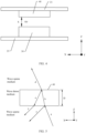
- FIG. 5 is a schematic diagram of a transmission path, in the wave dense medium 40, of an electromagnetic wave emitted by the antenna 30 in the communications device 100 shown in FIG. 4 .
- an electromagnetic wave a emitted by the antenna 30 enters the wave dense medium 40 from a wave sparse medium located on the side that is of the wave dense medium 40 and that is close to the antenna 30, the electromagnetic wave undergoes wavelength division for the first time.
- a transmitted electromagnetic wave is a first transmitted electromagnetic wave b
- a reflected electromagnetic wave is a first reflected electromagnetic wave c.
- the first transmitted electromagnetic wave b passes through the wave dense medium 40 and enters a wave sparse medium located on the side that is of the wave dense medium 40 and that is away from the antenna 30, and undergoes wavelength division for the second time.
- a transmitted electromagnetic wave is a second transmitted electromagnetic wave d, and a reflected electromagnetic wave is a second reflected electromagnetic wave e.
- the second reflected electromagnetic wave e reversely passes through the wave dense medium 40 and enters the wave sparse medium located on the side that is of the wave dense medium 40 and that is close to the antenna 30, and a transmitted electromagnetic wave is a third transmitted electromagnetic wave f.
- ⁇ g ⁇ 0 / DK
- ⁇ 0 a resonance wavelength of the operating band of the antenna 30 in a vacuum
- ⁇ 0 C 0 /F
- C 0 is a transmission speed of the electromagnetic wave in the vacuum
- C 0 3 ⁇ 10 ⁇ 8m/s
- F is the operating band of the antenna 30, and F represents a band range. For example, if the operating band of the antenna 30 is a band n257, F is 26.5 GHz-29.5 GHz.
- ⁇ 0 is also a wavelength range, and is specifically an upper limit of a C 0 /F band range to a lower limit of the C 0 /F band range.
- DK is the dielectric constant of the wave dense medium 40, and wave dense media 40 of different materials have different values of DK. Therefore, ⁇ g is also a wavelength range. It can be learned that a condition satisfied by the thickness D is: 0.5n ⁇ g(1-10%) ⁇ D ⁇ 0.5n ⁇ g(1+10%). In other words, the thickness D satisfies 0.5n ⁇ g1(1-10%) ⁇ D ⁇ 0.5n ⁇ g2(1+10%).
- ⁇ g1 is a resonance wavelength of an upper-limit frequency in the operating band of the antenna 30 in the wave dense medium 40
- ⁇ g2 is a resonance wavelength of a lower-limit frequency in the operating band of the antenna 30 in the wave dense medium 40.
- the thickness D of the wave dense medium 40 is an integral multiple of a half wavelength of the antenna 30 in the wave dense medium 40, and the wave dense medium 40 forms a Fabry-Perot resonator.
- the electromagnetic wave is reflected from the wave sparse medium to the wave dense medium, there is a phase difference of 180°, and when the electromagnetic wave is transmitted from the wave sparse medium to the wave dense medium, there is a phase difference of 0°.
- the electromagnetic wave is reflected from the wave dense medium to the wave sparse medium, there is a phase difference of 0°, and when the electromagnetic wave is transmitted from the wave dense medium to the wave sparse medium, there is a phase difference of 0°.
- the Fabry-Perot resonator can implement an anti-reflection effect, and can increase a gain of the antenna 30.
- n 1
- the wave dense medium 40 has a small thickness D, and can be installed in a communications device with limited space, to implement thinning of the communications device.
- the thickness D of the wave dense medium 40 may be less than or equal to 2 mm. In this way, installation of the wave dense medium 40 in the communications device with limited space can be facilitated, to ensure thinning of the communications device. Based on this, optionally, the thickness D of the wave dense medium 40 is further greater than or equal to 0.1 mm. In this way, structural strength of the wave dense medium 40 can be ensured without affecting thinning of the communications device, to facilitate installation in the communications device.
- the thickness D of the wave dense medium 40 may be 0.1 mm, 0.2 mm, 0.4 mm, 0.6 mm, 0.8 mm, 1.0 mm, 1.2 mm, 1.3 mm, 1.4 mm, 1.5 mm, 1.6 mm, 1.7 mm, 1.8 mm, 1.9 mm, or 2.0 mm.
- the antenna 30 when the antenna 30 is a mmWave band (for example, the band n257: 26.5 GHz-29.5 GHz; the band n258: 24.25 GHz-27.5 GHz; or the band n260: 37 GHz-40 GHz) antenna, the value of DK of the wave dense medium 40 may be greater than or equal to 14 and less than or equal to 40.
- a spacing (to be specific, a height h of an air gap) between the wave dense medium 40 and the antenna 30 is greater than 0 mm and less than 10 mm.
- the height h is greater than 0.02 mm and less than 3 mm. In this way, small impact is exerted on thinning of the communications device 100, and an effect of increasing the gain of the antenna 30 by the wave dense medium 40 is better.
- the height h is greater than or equal to 0.5 mm and less than or equal to 1 mm. In this way, smaller impact is exerted on thinning of the communications device 100, and an effect of increasing the gain of the antenna 30 by the wave dense medium 40 is better.
- an orthogonal projection of the antenna 30 on the back cover 21 is a first projection
- an orthogonal projection of the wave dense medium 40 on the back cover 21 is a second projection
- the first projection overlaps the second projection.
- the wave dense medium 40 is located in the transmission direction of the antenna 30, and is directly opposite to the antenna 30, so that the gain of the antenna 30 can be increased. That the first projection overlaps the second projection indicates that a part of the first projection overlaps a part of the second projection; or the entire first projection overlaps a part of the second projection; or a part of the first projection overlaps the entire second projection; or the entire first projection overlaps the entire second projection.
- an area of the second projection is greater than an area of the first projection, an edge of the second projection is located outside an edge of the first projection, and the edge of the second projection and the edge of the first projection are spaced apart.
- FIG. 6 is a schematic diagram of an orthogonal projection (that is, a first projection O1) of the antenna 30 on the back cover 21 and an orthogonal projection (that is, a second projection O2) of the wave dense medium 40 on the back cover 21 in the communications device 100 shown in FIG. 2 and FIG. 3 .
- Both the first projection O1 and the second projection O2 are rectangular, a length direction of the first projection O1 is the same as a length direction of the second projection O2, and a width direction of the first projection O1 is the same as a width direction of the second projection O2.
- the first projection O1 is located within the second projection O2, a length L1 of the first projection O1 is less than a length L2 of the second projection O2, a width W1 of the first projection O1 is less than a width W2 of the second projection O2, and an edge C1 of the first projection O1 and an edge C2 of the second projection O2 are spaced apart.
- a size of the wave dense medium 40 exceeds a size of the antenna 30, and the wave dense medium 40 can cover the antenna 30, so that the gain of the antenna 30 can be increased as much as possible.
- FIG. 7 shows input return losses S11 of the antenna 30 that exist when no wave dense medium 40 is disposed and when the wave dense medium 40 is disposed in the communications device 100 shown in FIG. 1 to FIG. 3 .
- S11_no F-P indicates an input return loss that is of the antenna 30 and that exists when no wave dense medium 40 is disposed in the communications device 100
- S11_0.25 ⁇ g indicates an input return loss that is of the antenna 30 and that exists when the wave dense medium 40 is disposed in the communications device 100 and a thickness of the wave dense medium 40 is 0.25 ⁇ g
- S11_0.5 ⁇ g indicates an input return loss that is of the antenna 30 and that exists when the wave dense medium 40 is disposed in the communications device 100 and a thickness of the wave dense medium 40 is 0.5 ⁇ g
- S11_0.75 ⁇ g indicates an input return loss that is of the antenna 30 and that exists when the wave dense medium 40 is disposed in the communications device 100 and a thickness of the wave dense medium 40 is 0.75 ⁇ g.
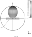
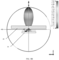
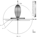
- FIG. 8A and FIG. 8B are directivity diagrams of the antenna 30 at 26 GHz when no wave dense medium 40 is disposed and when the wave dense medium 40 is disposed in the communications device 100 shown in FIG. 1-FIG. 3 .
- FIG. 8A is a directivity diagram of the antenna 30 at 26 GHz when no wave dense medium 40 is disposed
- FIG. 8B is a directivity diagram of the antenna 30 at 26 GHz when the wave dense medium 40 is disposed.
- a thickness of the wave dense medium 40 is close to 0.5 ⁇ g. It can be learned from FIG. 8A that when no wave dense medium 40 is disposed, the gain (gain) of the antenna 30 is 3.6 dBi; and it can be learned from FIG. 8B that when the wave dense medium 40 is disposed, the gain of the antenna 30 is 7.8 dBi. The gain is increased by approximately 4.2 dBi.
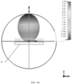
- FIG. 9A and FIG. 9B are directivity diagrams of the antenna 30 at 28 GHz when no wave dense medium 40 is disposed and when the wave dense medium 40 is disposed in the communications device 100 shown in FIG. 1-FIG. 3 .
- FIG. 9A is a directivity diagram of the antenna 30 at 28 GHz when no wave dense medium 40 is disposed
- FIG. 9B is a directivity diagram of the antenna 30 at 28 GHz when the wave dense medium 40 is disposed.
- a thickness of the wave dense medium 40 is close to 0.5 ⁇ g. It can be learned from FIG. 9A that when no wave dense medium 40 is disposed, the gain (gain) of the antenna 30 is 3.7 dBi; and it can be learned from FIG. 8B that when the wave dense medium 40 is disposed, the gain of the antenna 30 is 8.1 dBi. The gain is increased by approximately 4.4 dBi.
- the size of the wave dense medium 40 exceeds the size of the antenna 30, and a size of a reference ground layer of the modular antenna 30 is less than or equal to the size of the antenna 30, the size of the wave dense medium 40 exceeds the size of the reference ground layer of the antenna 30. Based on this, the size of the reference ground layer may be increased, so that energy that is of an electromagnetic field and that extends outwards in the wave dense medium 40 is emitted as much as possible in a direction in which the wave dense medium 40 is away from the reference ground layer, to further increase the gain of the antenna 30.
- the reference ground layer of the antenna 30 may be electrically connected to the middle plate 23 with a large size or a reference ground layer in the circuit board, to increase the size of the reference ground layer of the antenna 30, so as to further increase the gain of the antenna 30.
- FIG. 10 is a directivity diagram of the antenna 30 at 26 GHz when the wave dense medium 40 is disposed in the communications device 100 shown in FIG. 1-FIG. 3 and after the size of the reference ground layer of the antenna 30 is optimized.
- FIG. 11 is a directivity diagram of the antenna 30 at 28 GHz when the wave dense medium 40 is disposed in the communications device 100 shown in FIG. 1-FIG. 3 and after the size of the reference ground layer of the antenna 30 is optimized. It can be learned from FIG. 10 and FIG.
- the gain of the antenna 30 at 26 GHz is increased from 7.8 dBi to 14.1 dBi, and the gain of the antenna 30 at 28 GHz is increased from 8.1 dBi to 17.8 dBi. Therefore, the gain of the antenna 30 is further increased.
- FIG. 12 is a directivity diagram of the antenna 30 at 26 GHz when no wave dense medium 40 is disposed in the communications device 100 shown in FIG. 1-FIG. 3 but the size of the reference ground layer of the antenna 30 is optimized.
- FIG. 13 is a directivity diagram of the antenna 30 at 28 GHz when no wave dense medium 40 is disposed in the communications device 100 shown in FIG. 1-FIG. 3 but the size of the reference ground layer of the antenna 30 is optimized. It can be learned from FIG. 12 and FIG. 13 that the gain is slightly increased after the size of the reference ground layer of the antenna 30 is optimized.
- the gain of the antenna 30 is increased from 3.6 dBi to 3.8 dBi at 26 GHz, and the gain of the antenna 30 is increased from 3.7 dBi to 4.0 dBi at 28 GHz.
- the directivity diagram is also distorted. It can be learned that, when the wave dense medium 40 is disposed, the size of the reference ground layer of the antenna 30 is further optimized, so that the gain can be greatly increased.
- the antenna 30 may transmit a signal to the side that is of the back cover 21 and that is away from the screen 10 and the wave dense medium 40 is disposed on the inner surface of the back cover 21 .
- the wave dense medium 40 may be disposed in the region that is on the back cover 21 and that is opposite to the antenna 30, or may be disposed on the side that is of the back cover 21 and that is away from the antenna 30.
- the antenna 30 may transmit a signal to the side that is of the frame 22 and that is away from the internal accommodation space of the communications device 100, or transmit a signal to the side that is of the screen 10 and that is away from the back cover 21.
- the wave dense medium 40 may be disposed on an inner surface of the frame 22 or the screen 10, in the region opposite to the antenna 30, or on the side that is away from the antenna 30.
- FIG. 14 is a schematic diagram of relative positions of the middle plate 23, the back cover 21, the antenna 30, and the wave dense medium 40 in the communications device 100 according to some other embodiments of this application.
- the wave dense medium 40 is built in the region that is on the back cover 21 and that is opposite to the antenna 30. In this way, a thickness of the communications device can be reduced, and thinning of the communications device can be facilitated.
- a hole that is on the back cover 21 and that is used to build the wave dense medium 40 may be a blind hole, or may be a through hole.
- the blind hole may penetrate through an inner surface of the back cover 21, and may not penetrate through an outer surface of the back cover 21; or may penetrate through an outer surface of the back cover 21, and may not penetrate through an inner surface of the back cover 21. This is not specifically limited herein.
- the hole that is on the back cover 21 and that is used to build the wave dense medium 40 is a blind hole
- the blind hole penetrates through the inner surface of the back cover 21, and does not penetrate through the outer surface of the back cover 21
- a part of the wave dense medium 40 is located on an inner side of the back cover 21, and the other part is built into the blind hole.
- the hole that is on the back cover 21 and that is used to build the wave dense medium 40 is a blind hole
- the blind hole penetrates through the outer surface of the back cover 21, and does not penetrate through the inner surface of the back cover 21, a part of the wave dense medium 40 is located on an outer side of the back cover 21, and the other part is built into the blind hole.
- a surface that is of the wave dense medium 40 and that is away from the antenna 30 may be flush with an outer surface of the back cover 21, or may protrude to an outer side of the back cover 21.
- the surface that is of the wave dense medium 40 and that is away from the antenna 30 is flush with the outer surface of the back cover 21. In this way, appearance neatness of the communications device 100 can be improved.
- the outer surface of the back cover 21 is the surface that is of the back cover 21 and that is away from the internal accommodation space of the communications device 100, that is, the surface that is of the back cover 21 and that is away from the screen 10.
- the outer side of the back cover 21 is a side that is of the outer surface of the back cover 21 and that is away from an inner surface of the back cover 21.
- an inner side of the back cover 21 is a side that is of the inner surface of the back cover 21 and that is away from the outer surface of the back cover 21.
- a wave sparse medium located on a side that is of the wave dense medium 40 and that is close to the antenna 30 is air
- a wave sparse medium located on a side that is of the wave dense medium 40 and that is away from the antenna 30 is also air.
- a dielectric constant DK of air is small and is approximately 1, and therefore, small impact is exerted on an F-P effect of the wave dense medium 40.
- FIG. 15 is a schematic diagram of relative positions of the middle plate 23, the back cover 21, the antenna 30, and the wave dense medium 40 in the communications device 100 according to some other embodiments of this application.
- the wave dense medium 40 includes a first part 41 and a second part 42.
- the first part 41 includes a partial region of the back cover 21.
- the second part 42 is located between the first part 41 and the antenna 30, and the second part 42 is disposed on a surface (that is, an inner surface of the first part 41) that is of the first part 41 and that is close to the antenna 30.
- a sum of a thickness of the first part 41 and a thickness of the second part 42 is the thickness D of the wave dense medium 40, and this also facilitates thinning of the communications device.
- the second part 42 is disposed on a surface that is of the first part 41 and that is close to the antenna 30, an appearance of the communications device is not affected.
- the second part 42 may alternatively be disposed on a surface (that is, an outer surface of the first part 41) that is of the first part 41 and that is away from the antenna 30.
- FIG. 16 is a schematic diagram of relative positions of the middle plate 23, the back cover 21, the antenna 30, and the wave dense medium 40 in the communications device 100 according to some other embodiments of this application.
- a part of the second part 42 is disposed on the inner surface of the first part 41, and the other part is disposed on the outer surface of the first part 41.
- the first part 41 and the second part 42 are integrally formed. In this way, complexity of a composition structure of the communications device can be reduced, and assembly efficiency can be improved.
- a wave sparse medium located on the side that is of the wave dense medium 40 and that is close to the antenna 30 is air
- a wave sparse medium located on the side that is of the wave dense medium 40 and that is away from the antenna 30 is also air.
- a dielectric constant DK of air is small and is approximately 1, and therefore, small impact is exerted on an F-P effect of the wave dense medium 40.
- FIG. 17 is a schematic diagram of relative positions of the middle plate 23, the back cover 21, the antenna 30, and the wave dense medium 40 in the communications device 100 according to some other embodiments of this application.
- the wave dense medium 40 is located on the side that is of the back cover 21 and that is away from the antenna 30.
- the wave dense medium 40 is located on the outer side of the back cover 21.
- the wave dense medium 40 is disposed on the outer surface of the back cover 21. In this way, the wave dense medium 40 does not occupy the internal accommodation space of the communications device, to avoid compressing installation space of another component in the communications device.
- a wave sparse medium located on the side that is of the wave dense medium 40 and that is close to the antenna 30 is the back cover 21, and a wave sparse medium located on the side that is of the wave dense medium 40 and that is away from the antenna 30 is air.
- a material of the back cover 21 may be plastic or glass, and the plastic and the glass each have a small dielectric constant, and each exert small impact on an F-P effect of the wave dense medium 40.
- FIG. 18 is a schematic diagram of a structure of a rear face of the communications device 100 according to some other embodiments of this application.
- the communications device 100 further includes a camera decoration element 50, and the camera decoration element 50 is disposed on the back cover 21.
- a signal transmission direction of the antenna 30 points to the camera decoration element 50.
- FIG. 19 is a schematic diagram of a cross-sectional structure of the communications device 100 shown in FIG. 18 in a direction B-B.
- the camera decoration element 50 includes a decoration element body 51 and a light-transmitting plate 52 disposed on a side that is of the decoration element body 51 and that is away from the antenna 30.
- the decoration element body 51 is provided with a first mounting hole 5 1a.
- a part of the wave dense medium 40 is located on a side that is of the camera decoration element 50 and that is close to the antenna 30, and the other part of the wave dense medium 40 is mounted in the first mounting hole 51a of the decoration element body 51. In this way, a thickness of the communications device 100 can be reduced to some extent, and appearance consistency of the camera decoration part 50 can be ensured.
- FIG. 20 is a schematic diagram of relative positions of the middle plate 23, the camera decoration element 50, the antenna 30, and the wave dense medium 40 in the communications device 100 according to some other embodiments of this application.
- the decoration element body 51 is provided with the first mounting hole 51a
- the light-transmitting plate 52 is provided with a second mounting hole 52a.
- a part of the wave dense medium 40 is installed in the first mounting hole 51a of the decoration element body 51
- a part of the wave dense medium 40 is installed in the second mounting hole 52a of the light-transmitting plate 52
- a remaining part of the wave dense medium 40 is located on a side that is of the camera decoration element 50 and that is close to the antenna 30. In this way, a thickness of the communications device 100 can be greatly reduced.
- FIG. 21 is a schematic diagram of relative positions of the middle plate 23, the camera decoration element 50, the antenna 30, and the wave dense medium 40 in the communications device 100 according to some other embodiments of this application.
- the wave dense medium 40 is located on a side that is of the camera decoration element 50 and that is away from the antenna 30.
- the wave dense medium 40 is located on an outer side of the camera decoration element 50.
- the wave dense medium 40 is disposed on an outer surface of the camera decoration element 50. In this way, the wave dense medium 40 does not occupy the internal accommodation space of the communications device, to avoid compressing installation space of another component in the communications device.
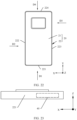
- FIG. 22 is a schematic diagram of a structure of a rear face of the communications device 100 according to some other embodiments of this application.
- the frame 22 includes a lower frame 221, a left frame 222, a right frame 223, and an upper frame 224.
- FIG. 23 is a schematic diagram of a structure existing when the communications device 100 shown in FIG. 22 is viewed from a direction D1.
- the antenna 30 transmits a signal to a side that is of the lower frame 221 and that is away from the internal accommodation space of the communications device 100, and the wave dense medium 40 is disposed on an inner surface of the lower frame 221, is built into the lower frame 221, is integrally formed with the lower frame 221, or is disposed on an outer surface of the lower frame 221.
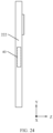
- FIG. 24-FIG. 26 reference is made to FIG. 24-FIG. 26 .
- FIG. 24 is a schematic diagram of a structure existing when the communications device 100 shown in FIG. 22 is viewed from a direction D2.
- FIG. 25 is a schematic diagram of a structure existing when the communications device 100 shown in FIG. 22 is viewed from a direction D3.
- FIG. 24 is a schematic diagram of a structure existing when the communications device 100 shown in FIG. 22 is viewed from a direction D2.
- the antenna 30 may transmit a signal to a side that is of the left frame 222, the right frame 223, or the upper frame 224 and that is away from the internal accommodation space of the communications device 100.
- the wave dense medium 40 is disposed on an inner surface of the left frame 222, the right frame 223, or the upper frame 224, is built into the left frame 222, the right frame 223, or the upper frame 224, or is disposed on an outer surface of the left frame 222, the right frame 223, or the upper frame 224.
- a corresponding wave dense medium 40 may be separately disposed for each antenna 30; or a same wave dense medium 40 may be disposed for the plurality of antennas 30, and the wave dense medium 40 may cover the plurality of antennas 30, to increase gains of the plurality of antennas 30. This is not specifically limited herein.
- FIG. 27 is a schematic diagram of relative positions of the antenna 30, the wave dense medium 40, and the middle plate 23 in the communications device 100 according to some other embodiments of this application.
- the bearing medium 31 may be formed by sequentially alternating and stacking an insulating medium layer and a metal layer, and the antenna 30 includes a metal layer in the bearing medium 31 and a metal via hole connected between a plurality of metal layers.
- Each antenna 30 corresponds to one wave dense medium 40, and wave dense media 40 corresponding to the plurality of antennas 30 are independent of each other. In this way, a single wave dense medium 40 has a small volume, and the single wave dense medium 40 has low costs.
- FIG. 28 is a schematic diagram of relative positions of the antenna 30, the wave dense medium 40, and the middle plate 23 in the communications device 100 according to some other embodiments of this application.
- the plurality of antennas 30 correspond to a same wave dense medium 40, and the wave dense medium 30 can cover the plurality of antennas 30, to increase gains of the plurality of antennas 30. In this way, there is a quantity of wave dense media 40, complexity of a composition structure of the communications device is low, assembly difficulty is small, and efficiency is high.
Landscapes
- Engineering & Computer Science (AREA)
- Computer Networks & Wireless Communication (AREA)
- Aerials With Secondary Devices (AREA)
- Details Of Aerials (AREA)
- Support Of Aerials (AREA)
Abstract
Description
- This application claims priority to
Chinese Patent Application No. 202210103508.9, filed with the China National Intellectual Property Administration on January 27, 2022 - This application relates to the field of antenna technologies, and in particular, to a communications device with an antenna.
- Currently, signals on frequency bands such as a Sub-6 GHz band, a millimeterwave (mmWave) band, and a terahertz (THz) band are attenuated to different degrees in a process of being transmitted in space. To improve a coverage area of a device (a base station or a terminal), a gain of an antenna is usually increased. To increase the gain of the antenna, a shape, a material, or a size of the antenna may be optimized. However, an antenna such as a mmWave antenna has a small size, and tends to be modular. If a shape, a material, or a size of the antenna is changed, manufacturing difficulty and costs of the antenna are greatly increased, and consequently, a gain of the antenna is difficult to increase.
- Embodiments of this application provide a communications device, to increase a gain of an antenna without interfering with modularization of the antenna.
- To achieve the foregoing objective, an embodiment of this application provides a communications device. The communications device includes an antenna and a wave dense medium. The wave dense medium is located in a transmission direction of the antenna and is spaced apart from the antenna, a dielectric constant of a medium, in the communications device, located on a side that is of the wave dense medium and that is close to the antenna and a dielectric constant of a medium located on a side that is of the wave dense medium and that is away from the antenna are both less than a dielectric constant of the wave dense medium, and a thickness D of the wave dense medium from a surface that is close to the antenna to a surface that is away from the antenna satisfies 0.5nλg(1-10%)≤D≤0.5nλg(1+10%), where n=1, 2, 3, ..., and λg is a resonance wavelength of an operating band of the antenna in the wave dense medium.
- Because the dielectric constant of the medium, in the communications device, located on the side that is of the wave dense medium and that is close to the antenna and the dielectric constant of the medium located on the side that is of the wave dense medium and that is away from the antenna are both less than the dielectric constant of the wave dense medium, compared with the wave dense medium, the medium located on the side that is of the wave dense medium and that is close to the antenna and the medium located on the side that is of the wave dense medium and that is away from the antenna each have a lower dielectric constant, and each are a wave sparse medium. When an electromagnetic wave emitted by the antenna enters the wave dense medium from a wave sparse medium located on the side that is of the wave dense medium and that is close to the antenna, the electromagnetic wave undergoes wavelength division for the first time. It is assumed that a transmitted electromagnetic wave is a first transmitted electromagnetic wave, and a reflected electromagnetic wave is a first reflected electromagnetic wave. The first transmitted electromagnetic wave passes through the wave dense medium and enters a wave sparse medium located on the side that is of the wave dense medium and that is away from the antenna, and undergoes wavelength division for the second time. During wavelength division in the second time, a transmitted electromagnetic wave is a second transmitted electromagnetic wave, and a reflected electromagnetic wave is a second reflected electromagnetic wave. The second reflected electromagnetic wave reversely passes through the wave dense medium and enters the wave sparse medium located on the side that is of the wave dense medium and that is close to the antenna, and a transmitted electromagnetic wave is a third transmitted electromagnetic wave. Based on this, because the thickness D of the wave dense medium from the surface that is close to the antenna to the surface that is away from the antenna satisfies 0.5nλg(1-10%)≤D≤0.5nλg(1+10%), where n=1, 2, 3, ..., and λg is the resonance wavelength of the operating band of the antenna in the wave dense medium, the thickness of the wave dense medium is an integral multiple of a half wavelength of the antenna in the wave dense medium. The wave dense medium forms a Fabry-Perot resonator. When the electromagnetic wave is reflected from the wave sparse medium to the wave dense medium, there is a phase difference of 180°, and when the electromagnetic wave is transmitted from the wave sparse medium to the wave dense medium, there is a phase difference of 0°. When the electromagnetic wave is reflected from the wave dense medium to the wave sparse medium, there is a phase difference of 0°, and when the electromagnetic wave is transmitted from the wave dense medium to the wave sparse medium, there is a phase difference of 0°. To be specific, there is a phase difference of 180° between the first reflected electromagnetic wave and the electromagnetic wave emitted by the antenna, there is a phase difference of 0° between the electromagnetic wave emitted by the antenna and the first transmitted electromagnetic wave, there is a phase difference of 0° between the first transmitted electromagnetic wave and the second reflected electromagnetic wave, and there is a phase difference of 0° between the second reflected electromagnetic wave and the third transmitted electromagnetic wave. Therefore, there is exactly a phase difference of 180° between the first reflected electromagnetic wave and the third transmitted electromagnetic wave, and this is represented as interference cancelation. Therefore, the Fabry-Perot resonator can implement an anti-reflection effect, and can increase a gain of the antenna.
- In a possible implementation, n=1. In this way, the wave dense medium has a small thickness D, and can be installed in a communications device with limited space, to implement thinning of the communications device.
- In a possible implementation, the thickness D of the wave dense medium is less than or equal to 2 mm. In this way, installation of the wave dense medium in the communications device with limited space can be facilitated, to ensure thinning of the communications device.
- In a possible implementation, the thickness D of the wave dense medium is further greater than or equal to 0.1 mm. In this way, structural strength of the wave
dense medium 40 can be ensured, to facilitate installation in the communications device. - In a possible implementation, the thickness D of the wave dense medium may be 0.1 mm, 0.2 mm, 0.4 mm, 0.6 mm, 0.8 mm, 1.0 mm, 1.2 mm, 1.3 mm, 1.4 mm, 1.5 mm, 1.6 mm, 1.7 mm, 1.8 mm, 1.9 mm, or 2.0 mm.
- In a possible implementation, the dielectric constant DK of the wave dense medium is greater than or equal to 14 and less than or equal to 40. In this way, when n=1 and the antenna is a mmWave band antenna, the operating band of the antenna is within 24 GHz~40 GHz, and the thickness D of the wave dense medium is approximately 1 mm. The structural strength of the wave dense medium can be ensured without affecting thinning of the communications device.
- In a possible implementation, a material of the wave dense medium is zirconia ceramic. A dielectric constant DK of the zirconia ceramic is 30. When n=1, the thickness D of the wave dense medium is approximately 1 mm, so that the structural strength of the wave dense medium can be ensured without affecting thinning of the communications device.
- In a possible implementation, the antenna and the wave dense medium are spaced apart by air, and the air forms the medium, in the communications device, located on the side that is of the wave dense medium and that is close to the antenna. The air has a small dielectric constant, and exerts small impact on a Fabry-Perot effect of the wave dense medium.
- In a possible implementation, a spacing between the antenna and the wave dense medium is greater than 0 mm and less than 10 mm. In this way, small impact is exerted on thinning of the communications device, and an effect of increasing the gain of the antenna by the wave dense medium is good.
- In a possible implementation, the spacing between the antenna and the wave dense medium is greater than 0.02 mm and less than 3 mm. In this way, small impact is exerted on thinning of the communications device, and the effect of increasing the gain of the antenna by the wave dense medium is better.
- In a possible implementation, the spacing between the antenna and the wave dense medium is greater than or equal to 0.5 mm and less than or equal to 1 mm. In this way, smaller impact is exerted on thinning of the communications device, and the effect of increasing the gain of the antenna by the wave dense medium is better.
- In a possible implementation, the communications device further includes a back cover; and the antenna is located on an inner side of the back cover, the wave dense medium is located between the antenna and the back cover and is disposed on an inner surface of the back cover, and the back cover forms the medium, in the communications device, located on the side that is of the wave dense medium and that is away from the antenna. Based on this, optionally, a material of the back cover is plastic or glass. The plastic and the glass each have a small dielectric constant, and exert small impact on the Fabry-Perot effect of the wave dense medium.
- In a possible implementation, the communications device further includes a back cover; and the antenna is located on an inner side of the back cover, and the wave dense medium is built in a region that is on the back cover and that is opposite to the antenna. In this way, a thickness of the communications device can be reduced, and thinning of the communications device can be facilitated.
- In a possible implementation, a hole that is on the back cover and that is used to build the wave dense medium may be a blind hole, or may be a through hole. When the hole that is on the back cover and that is used to build the wave dense medium is a blind hole, the blind hole may penetrate through an inner surface of the back cover, and may not penetrate through an outer surface of the back cover; or may penetrate through an outer surface of the back cover, and may not penetrate through an inner surface of the back cover. This is not specifically limited herein. When the hole that is on the back cover and that is used to build the wave dense medium is a blind hole, and the blind hole penetrates through the inner surface of the back cover, and does not penetrate through the outer surface of the back cover, a part of the wave dense medium is located on the inner side of the back cover, and the other part is built into the blind hole. When the hole that is on the back cover and that is used to build the wave dense medium is a blind hole, and the blind hole penetrates through the outer surface of the back cover, and does not penetrate through the inner surface of the back cover, a part of the wave dense medium is located on an outer side of the back cover, and the other part is built into the blind hole.
- In a possible implementation, when the hole that is on the back cover and that is used to build the wave dense medium is a through hole, the surface that is of the wave dense medium and that is away from the antenna may be flush with the outer surface of the back cover, or may protrude to an outer side of the back cover. Optionally, the surface that is of the wave dense medium and that is away from the antenna is flush with the outer surface of the back cover. In this way, appearance neatness of the communications device can be improved.
- In a possible implementation, the communications device further includes a back cover. The antenna is located on an inner side of the back cover, the wave dense medium includes a first part and a second part, and the first part includes a partial region of the back cover; and the second part is located between the first part and the antenna, and the second part is disposed on an inner surface of the first part. In this way, a sum of a thickness of the first part and a thickness of the second part is the thickness of the wave dense medium, and this also facilitates thinning of the communications device. In addition, because the second part is disposed on a surface that is of the first part and that is close to the antenna, an appearance of the communications device is not affected.
- In a possible implementation, the second part may alternatively be located on a side that is of the first part and that is away from the antenna, and is disposed on an outer surface of the first part. Alternatively, a part of the second part is located between the first part and the antenna and is disposed on an inner surface of the first part, and the other part is located on a side that is of the first part and that is away from the antenna and is disposed on an outer surface of the first part.
- In a possible implementation, the first part and the second part are integrally formed. In this way, complexity of a composition structure of the communications device can be reduced, and assembly efficiency can be improved.
- In a possible implementation, the communications device further includes a back cover; and the antenna is located on an inner side of the back cover, the wave dense medium is located on an outer side of the back cover, and the wave dense medium is disposed on an outer surface of the back cover. In this way, the wave dense medium does not occupy internal accommodation space of the communications device, to avoid compressing installation space of another component in the communications device.
- In a possible implementation, an orthogonal projection of the antenna on the back cover is a first projection, and an orthogonal projection of the wave dense medium on the back cover is a second projection; and an area of the second projection is greater than an area of the first projection, an edge of the second projection is located outside an edge of the first projection, and the edge of the second projection and the edge of the first projection are spaced apart. In this way, a size of the wave dense medium exceeds a size of the antenna, the wave dense medium can cover the antenna, and the gain of the antenna can be increased as much as possible.
- In a possible implementation, the antenna is a millimeterwave band antenna. Compared with a Sub-6 GHz band, a millimeterwave band is characterized by a higher bandwidth, wider connections, a lower latency, and the like. However, a signal on the millimeterwave band is rapidly attenuated in space. Therefore, a gain needs to be increased urgently, to increase a coverage area of the communications device (for example, a base station or a terminal) on the millimeterwave band. In addition, compared with a terahertz band, the millimeterwave band is characterized by low costs, and therefore, has an advantage of a wide application range.
-
-
FIG. 1 is a schematic diagram of a structure of a front face of a communications device according to some embodiments of this application; -
FIG. 2 is a schematic diagram of a structure of a rear face of the communications device shown inFIG. 1 ; -
FIG. 3 is a schematic diagram of a cross-sectional structure of the communications device shown inFIG. 2 in a direction A-A; -
FIG. 4 is a schematic diagram of relative positions of a middle plate, a back cover, an antenna, and a wave dense medium in the communications device shown inFIG. 3 ; -
FIG. 5 is a schematic diagram of a transmission path, in a wave dense medium, of an electromagnetic wave emitted by an antenna in the communications device shown inFIG. 4 ; -
FIG. 6 is a schematic diagram of an orthogonal projection of an antenna on a back cover and an orthogonal projection of a wave dense medium on a back cover in the communications device shown inFIG. 2 and FIG. 3 ; -
FIG. 7 shows input return losses of an antenna that exist when no wave dense medium is disposed and when a wave dense medium is disposed in the communications device shown inFIG. 1 to FIG. 3 ; -
FIG. 8A andFIG. 8B are directivity diagrams of an antenna at 26 GHz when no wave dense medium is disposed and when a wave dense medium is disposed in the communications device shown inFIG. 1 to FIG. 3 , whereFIG. 8A is a directivity diagram of the antenna at 26 GHz when no wave dense medium is disposed, andFIG. 8B is a directivity diagram of the antenna at 26 GHz when a wave dense medium is disposed; -
FIG. 9A andFIG. 9B are directivity diagrams of an antenna at 28 GHz when no wave dense medium is disposed and when a wave dense medium is disposed in the communications device shown inFIG. 1 to FIG. 3 , whereFIG. 9A is a directivity diagram of the antenna at 28 GHz when no wave dense medium is disposed; andFIG. 9B is a directivity diagram of the antenna at 28 GHz when a wave dense medium is disposed; -
FIG. 10 is a directivity diagram of an antenna at 26 GHz when a wave dense medium is disposed in the communications device shown inFIG. 1 to FIG. 3 and after a size of a reference ground layer of the antenna is optimized; -
FIG. 11 is a directivity diagram of an antenna at 28 GHz when a wave dense medium is disposed in the communications device shown inFIG. 1 to FIG. 3 and after a size of a reference ground layer of the antenna is optimized; -
FIG. 12 is a directivity diagram of an antenna at 26 GHz when no wave dense medium is disposed in the communications device shown inFIG. 1 to FIG. 3 but a size of a reference ground layer of the antenna is optimized; -
FIG. 13 is a directivity diagram of an antenna at 28 GHz when no wave dense medium is disposed in the communications device shown inFIG. 1 to FIG. 3 but a size of a reference ground layer of the antenna is optimized; -
FIG. 14 is a schematic diagram of relative positions of a middle plate, a back cover, an antenna, and a wave dense medium in a communications device according to some other embodiments of this application; -
FIG. 15 is a schematic diagram of relative positions of a middle plate, a back cover, an antenna, and a wave dense medium in a communications device according to some other embodiments of this application; -
FIG. 16 is a schematic diagram of relative positions of a middle plate, a back cover, an antenna, and a wave dense medium in a communications device according to some other embodiments of this application; -
FIG. 17 is a schematic diagram of relative positions of a middle plate, a back cover, an antenna, and a wave dense medium in a communications device according to some other embodiments of this application; -
FIG. 18 is a schematic diagram of a structure of a rear face of a communications device according to some other embodiments of this application; -
FIG. 19 is a schematic diagram of a cross-sectional structure of the communications device shown inFIG. 18 in a direction B-B; -
FIG. 20 is a schematic diagram of relative positions of a middle plate, a camera decoration element, an antenna, and a wave dense medium in a communications device according to some other embodiments of this application; -
FIG. 21 is a schematic diagram of relative positions of a middle plate, a camera decoration element, an antenna, and a wave dense medium in a communications device according to some other embodiments of this application; -
FIG. 22 is a schematic diagram of a structure of a rear face of a communications device according to some other embodiments of this application; -
FIG. 23 is a schematic diagram of a structure existing when the communications device shown inFIG. 22 is viewed from a direction D1; -
FIG. 24 is a schematic diagram of a structure existing when the communications device shown inFIG. 22 is viewed from a direction D2; -
FIG. 25 is a schematic diagram of a structure existing when the communications device shown inFIG. 22 is viewed from a direction D3; -
FIG. 26 is a schematic diagram of a structure existing when the communications device shown inFIG. 22 is viewed from a direction D4; -
FIG. 27 is a schematic diagram of relative positions of an antenna, a wave dense medium, and a middle plate in a communications device according to some other embodiments of this application; and -
FIG. 28 is a schematic diagram of relative positions of an antenna, a wave dense medium, and a middle plate in a communications device according to some other embodiments of this application. - In the embodiments of this application, the terms "include", "have", and any other variant thereof are intended to cover non-exclusive inclusion, so that a process, method, article, or apparatus that includes a series of elements includes not only those elements but also other elements that are not explicitly listed, or includes elements inherent to such a process, method, article, or apparatus. Without more limitations, elements defined by the sentence "including a" does not exclude that there is still another same element in the process, method, object, or apparatus which includes the element.
- To increase a gain of an antenna without interfering with modularization of the antenna, a resonator is disposed in a transmission direction of the antenna based on a Fabry-Perot effect (also referred to as an F-P effect) in this application, so that based on an existing modular antenna, the gain of the antenna can be increased without a need to change a shape, a material, and a size of the antenna. Therefore, initial performance of the modular antenna does not need to be interfered with.
- The following describes the embodiments of this application in detail with reference to the accompanying drawings. In addition, before the embodiments of this application are described, an application scenario of the embodiments of this application is first described.
- This application provides a communications device. The communications device is a communications device having a wireless signal receiving and sending function. Specifically, the communications device may be a portable electronic apparatus or another proper electronic apparatus. For example, the communications device may be a mobile phone, a base station, a tablet computer (tablet personal computer), a notebook computer, a laptop computer (laptop computer), a personal digital assistant (personal digital assistant, PDA), or a wearable device. The wearable device includes but is not limited to a wristband, a watch, augmented reality (augmented reality, AR) glasses, an AR helmet, virtual reality (virtual reality, VR) glasses, a VR helmet, or the like.
- Refer to
FIG. 1-FIG. 3 .FIG. 1 is a schematic diagram of a structure of a front face of acommunications device 100 according to some embodiments of this application.FIG. 2 is a schematic diagram of a structure of a rear face of thecommunications device 100 shown inFIG. 1 .FIG. 3 is a schematic diagram of a cross-sectional structure of thecommunications device 100 shown inFIG. 2 in a direction A-A. This embodiment and the following embodiments are all described by using an example in which thecommunications device 100 is a mobile phone, and this cannot be considered as a special limitation on thecommunications device 100. Thecommunications device 100 includes ascreen 10, aback housing 20, a circuit board (not shown in the figure), and anantenna 30. - For ease of description of the following embodiments, an XYZ coordinate system is established. Specifically, it is defined that a length direction of the
communications device 100 is a Y-axis direction, a width direction is an X-axis direction, and a thickness direction is a Z-axis direction. It can be understood that a coordinate system of thecommunications device 100 may be flexibly set based on an actual requirement. This is not specifically limited herein. - The
screen 10 is configured to display an image, a video, or the like. Thescreen 10 includes a light-transmittingcover plate 11 and adisplay 12. The light-transmittingcover plate 11 and thedisplay 12 are stacked and fixedly connected. The light-transmittingcover plate 11 is mainly configured to protect thedisplay 12 and prevent dust. A material of the light-transmittingcover plate 11 includes but is not limited to glass. Thedisplay 12 may be a flexible display, or may be a rigid display. For example, thedisplay 12 may be an organic light-emitting diode (organic light-emitting diode, OLED) display, an active-matrix organic light-emitting diode or an active-matrix organic light-emitting diode (active-matrix organic light-emitting diode, AMOLED) display, a mini light-emitting diode (mini organic light-emitting diode) display, a micro light-emitting diode (micro organic light-emitting diode) display, a micro organic light-emitting diode (micro organic light-emitting diode) display, a quantum dot light emitting diode (quantum dot light emitting diodes, QLED) display, or a liquid crystal display (liquid crystal display, LCD). - The
back housing 20 is configured to protect an internal electronic component of thecommunications device 100. Theback housing 20 includes aback cover 21 and aframe 22. A material of theback cover 21 includes but is not limited to glass, plastic such as polycarbonate (polycarbonate, PC), and ceramic. Theback cover 21 is located on a side that is of thedisplay 12 and that is away from the light-transmittingcover plate 11, and is stacked with the light-transmittingcover plate 11 and thedisplay 12. Theframe 22 is located between theback cover 21 and the light-transmittingcover plate 11, and theframe 22 is fastened to theback cover 21. For example, theframe 22 may be fastened to theback cover 21 by using an adhesive. Theframe 22 may alternatively be integrally formed with theback cover 21. In other words, theframe 22 and theback cover 21 are of an integral structure. The light-transmittingcover plate 11 is fastened to theframe 22. In some embodiments, the light-transmittingcover plate 11 may be fastened to theframe 22 by using an adhesive. The light-transmittingcover plate 11, theback cover 21, and theframe 22 form internal accommodation space of thecommunications device 100. The internal accommodation space accommodates thedisplay 12. - In some embodiments, the
communications device 100 further includes amiddle plate 23. Themiddle plate 23 is disposed between thedisplay 12 and theback cover 21, and themiddle plate 23 is fastened to an inner surface of theframe 22. For example, themiddle plate 23 may be fastened to theframe 22 by using an adhesive, or themiddle plate 23 may be integrally formed with theframe 22. Themiddle plate 23 is made of a metal material, and themiddle plate 23 may be used as a reference ground of an electronic component in thecommunications device 100. - The circuit board is disposed in the internal accommodation space of the
communications device 100. In some embodiments, the circuit board is located between themiddle plate 23 and theback cover 21, and the circuit board is fastened to themiddle plate 23. The circuit board may be a primary circuit board, or may be a secondary circuit board. This is not specifically limited in this application. - The
antenna 30 is disposed in the internal accommodation space of thecommunications device 100. In some embodiments, as shown inFIG. 3 , theantenna 30 is disposed between themiddle plate 23 and theback cover 21. - In some embodiments, a radio frequency circuit is disposed on the circuit board, and the
antenna 30 is electrically connected to the radio frequency circuit on the circuit board, to transmit a radio frequency signal from the radio frequency circuit to external space in a form of an electromagnetic wave, so as to implement transmission of the signal; or receive an electromagnetic wave from external space, convert the electromagnetic wave into a radio frequency signal, and transmit the radio frequency signal to the radio frequency circuit, to implement receiving of the signal. - The
antenna 30 may be a directional antenna, or may be an omni-directional antenna. In some embodiments, as shown inFIG. 3 , theantenna 30 may transmit a signal to a side that is of theback cover 21 and that is away from thescreen 10. Based on this, theantenna 30 may be further configured to receive an electromagnetic wave signal from the side that is of theback cover 21 and that is away from thescreen 10. In some other embodiments, theantenna 30 may alternatively transmit a signal to a side that is of theframe 22 and that is away from the internal accommodation space of thecommunications device 100, or transmit a signal to a side that is of thescreen 10 and that is away from theback cover 21. In this embodiment, descriptions are provided by using an example in which theantenna 30 may transmit a signal to the side that is of theback cover 21 and that is away from thescreen 10. This cannot be considered as a special limitation on this application. - It should be noted that, when transmitting a signal to the side that is of the
back cover 21 and that is away from thescreen 10, theantenna 30 may further transmit a signal to another side, for example, transmit a signal to the side that is of theframe 22 and that is away from the internal accommodation space of thecommunications device 100, or transmit a signal to the side that is of thescreen 10 and that is away from theback cover 21. This is not specifically limited herein. - The
antenna 30 includes but is not limited to a Sub-6 GHz band antenna, a millimeterwave (mmWave) band antenna, and a terahertz (THz) band antenna. In some embodiments, theantenna 30 is a mmWave band antenna. A mmWave band is used as one of 5G mobile communication bands. Compared with a Sub-6 GHz band, the millimeterwave band is characterized by a higher bandwidth, wider connections, a lower latency, and the like. However, a signal on the mmWave band is rapidly attenuated in space. Therefore, a gain needs to be increased urgently, to increase a coverage area of the communications device (for example, a base station or a terminal) on the mmWave band. In addition, compared with a THz band, the mmWave band is characterized by low costs, and therefore, has an advantage of a wide application range. Specifically, when theantenna 30 is a mmWave band antenna, an operating band of theantenna 30 may be a band n257 (26.5 GHz-29.5 GHz), a band n258 (24.25 GHz-27.5 GHz), or a band n260 (37 GHz-40 GHz). This is not specifically limited herein. - To improve production efficiency of the communications device, the
antenna 30 may be used as a module for material supply. In this way, management is facilitated, and the production efficiency of the communications device including theantenna 30 can be improved. However, in this way, it is inconvenient to increase a gain of theantenna 30 by changing a shape, a material, or a size of theantenna 30. - Based on this, to increase the gain of the
antenna 30 without interfering with modularization of theantenna 30, as shown inFIG. 2 and FIG. 3 , the communications device further includes a wavedense medium 40. - The wave
dense medium 40 is a structure used to increase the gain of theantenna 30. In some embodiments, as shown inFIG. 3 , the wavedense medium 40 is in a rectangular sheet shape. In some other embodiments, the wave dense medium 40 may alternatively be in a circular sheet shape, an oval sheet shape, a triangular sheet shape, a polygonal sheet shape, or the like. - The wave
dense medium 40 is located in a transmission direction of theantenna 30, and the wavedense medium 40 is spaced apart from theantenna 30. Specifically, the wave dense medium 40 may be located between theantenna 30 and theback cover 21, or may be disposed in a region that is on theback cover 21 and that is opposite to theantenna 30, or may be disposed on a side that is of theback cover 21 and that is away from theantenna 30. In some embodiments, still as shown inFIG. 3 , the wavedense medium 40 is located between theantenna 30 and theback cover 21, and the wavedense medium 40 is disposed on an inner surface of theback cover 21. The inner surface of theback cover 21 is a surface that is of theback cover 21 and that faces the internal accommodation space of thecommunications device 100, that is, a surface that is of theback cover 21 and that is close to thescreen 10. Specifically, the wave dense medium 40 may be glued to the inner surface of theback cover 21, or may be directly formed on the inner surface of theback cover 21 by using theback cover 21 as a substrate. This is not specifically limited in this embodiment of this application. - The wave
dense medium 40 and theantenna 30 may be spaced apart by a solid medium, or may be spaced apart by air, or may be spaced apart by at least one layer of solid medium and at least one layer of air. This is not specifically limited herein. In some embodiments,FIG. 4 is a schematic diagram of relative positions of themiddle plate 23, theback cover 21, theantenna 30, and the wave dense medium 40 in thecommunications device 100 shown inFIG. 3 . The wavedense medium 40 and theantenna 30 are spaced apart by air. Such a structure is simple, costs of air are low, and it is easy to implement. - A value of a dielectric constant (DK, also referred to as relative permittivity) of a medium, in the
communications device 100, located on a side that is of the wavedense medium 40 and that is close to theantenna 30 and a value of DK of a medium located on a side that is of the wavedense medium 40 and that is away from theantenna 30 are both less than a value of DK of the wavedense medium 40. Specifically, the medium located on the side that is of the wavedense medium 40 and that is close to theantenna 30 is a medium that is adjacent to the wavedense medium 40 and that is located on the side that is of the wavedense medium 40 and that is close to theantenna 30. Similarly, the medium located on the side that is of the wavedense medium 40 and that is away from theantenna 30 is a medium that is adjacent to the wavedense medium 40 and that is located on the side that is of the wavedense medium 40 and that is away from theantenna 30. For example, as shown inFIG. 4 , the medium located on the side that is of the wavedense medium 40 and that is close to theantenna 30 is air, and the medium located on the side that is of the wavedense medium 40 and that is away from theantenna 30 is theback cover 21. In other words, a value of DK of air and a value of DK of theback cover 21 are both less than the value of DK of the wavedense medium 40. Based on this, plastic or glass with a small value of DK may be selected as a material of theback cover 21. In this way, relative to the wavedense medium 40, the medium located on the side that is of the wavedense medium 40 and that is close to theantenna 30 and the medium located on the side that is of the wavedense medium 40 and that is away from theantenna 30 each have a low dielectric constant, and each are a wave sparse medium. -
FIG. 5 is a schematic diagram of a transmission path, in the wavedense medium 40, of an electromagnetic wave emitted by theantenna 30 in thecommunications device 100 shown inFIG. 4 . When an electromagnetic wave a emitted by theantenna 30 enters the wave dense medium 40 from a wave sparse medium located on the side that is of the wavedense medium 40 and that is close to theantenna 30, the electromagnetic wave undergoes wavelength division for the first time. A transmitted electromagnetic wave is a first transmitted electromagnetic wave b, and a reflected electromagnetic wave is a first reflected electromagnetic wave c. The first transmitted electromagnetic wave b passes through the wavedense medium 40 and enters a wave sparse medium located on the side that is of the wavedense medium 40 and that is away from theantenna 30, and undergoes wavelength division for the second time. A transmitted electromagnetic wave is a second transmitted electromagnetic wave d, and a reflected electromagnetic wave is a second reflected electromagnetic wave e. The second reflected electromagnetic wave e reversely passes through the wavedense medium 40 and enters the wave sparse medium located on the side that is of the wavedense medium 40 and that is close to theantenna 30, and a transmitted electromagnetic wave is a third transmitted electromagnetic wave f. - Based on the foregoing embodiment, because a thickness D of the wave dense medium 40 from a surface that is close to the
antenna 30 to a surface that is away from theantenna 30 satisfies 0.5nλg(1-10%)≤D≤0.5nλg(1+10%), where n=1, 2, 3, ..., and λg is a resonance wavelength of an operating band of theantenna 30 in the wavedense medium 40. - Herein,
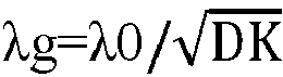
antenna 30 in a vacuum, λ0= C0/F, C0 is a transmission speed of the electromagnetic wave in the vacuum, C0 = 3 × 10^8m/s, F is the operating band of theantenna 30, and F represents a band range. For example, if the operating band of theantenna 30 is a band n257, F is 26.5 GHz-29.5 GHz. Based on this, λ0 is also a wavelength range, and is specifically an upper limit of a C0/F band range to a lower limit of the C0/F band range.DK is the dielectric constant of the wavedense medium 40, and wavedense media 40 of different materials have different values of DK. Therefore, λg is also a wavelength range. It can be learned that a condition satisfied by the thickness D is: 0.5nλg(1-10%)≤D≤0.5nλg(1+10%). In other words, the thickness D satisfies 0.5nλg1(1-10%)≤D≤0.5nλg2(1+10%). Herein, λg1 is a resonance wavelength of an upper-limit frequency in the operating band of theantenna 30 in the wavedense medium 40, and λg2 is a resonance wavelength of a lower-limit frequency in the operating band of theantenna 30 in the wavedense medium 40. - In this way, the thickness D of the wave
dense medium 40 is an integral multiple of a half wavelength of theantenna 30 in the wavedense medium 40, and the wave dense medium 40 forms a Fabry-Perot resonator. When the electromagnetic wave is reflected from the wave sparse medium to the wave dense medium, there is a phase difference of 180°, and when the electromagnetic wave is transmitted from the wave sparse medium to the wave dense medium, there is a phase difference of 0°. When the electromagnetic wave is reflected from the wave dense medium to the wave sparse medium, there is a phase difference of 0°, and when the electromagnetic wave is transmitted from the wave dense medium to the wave sparse medium, there is a phase difference of 0°. To be specific, there is a phase difference of 180° between the first reflected electromagnetic wave c and the electromagnetic wave a, there is a phase difference of 0° between the electromagnetic wave a and the first transmitted electromagnetic wave b, there is a phase difference of 0° between the first transmitted electromagnetic wave b and the second reflected electromagnetic wave e, and there is a phase difference of 0° between the second reflected electromagnetic wave e and the third transmitted electromagnetic wave f. Therefore, inFIG. 5 , there is exactly a phase difference of 180° between the first reflected electromagnetic wave b and the third transmitted electromagnetic wave f, and this is represented as interference cancelation. Therefore, the Fabry-Perot resonator can implement an anti-reflection effect, and can increase a gain of theantenna 30. - In some embodiments, n=1. In this way, the wave
dense medium 40 has a small thickness D, and can be installed in a communications device with limited space, to implement thinning of the communications device. - In some embodiments, the thickness D of the wave dense medium 40 may be less than or equal to 2 mm. In this way, installation of the wave dense medium 40 in the communications device with limited space can be facilitated, to ensure thinning of the communications device. Based on this, optionally, the thickness D of the wave
dense medium 40 is further greater than or equal to 0.1 mm. In this way, structural strength of the wave dense medium 40 can be ensured without affecting thinning of the communications device, to facilitate installation in the communications device. Specifically, the thickness D of the wave dense medium 40 may be 0.1 mm, 0.2 mm, 0.4 mm, 0.6 mm, 0.8 mm, 1.0 mm, 1.2 mm, 1.3 mm, 1.4 mm, 1.5 mm, 1.6 mm, 1.7 mm, 1.8 mm, 1.9 mm, or 2.0 mm. - To achieve the foregoing objective, when the
antenna 30 is a mmWave band (for example, the band n257: 26.5 GHz-29.5 GHz; the band n258: 24.25 GHz-27.5 GHz; or the band n260: 37 GHz-40 GHz) antenna, the value of DK of the wave dense medium 40 may be greater than or equal to 14 and less than or equal to 40. In this way, when n=1 and theantenna 30 is a mmWave band antenna, the operating band of theantenna 30 is within 24 GHz~40 GHz, and the thickness D of the wavedense medium 40 is approximately 1 mm. The structural strength of the wave dense medium 40 can be ensured without affecting thinning of the communications device. - In some embodiments, a material of the wave
dense medium 40 includes but is not limited to zirconia ceramic and alumina ceramic. Dielectric constants DK of the zirconia ceramic and the alumina ceramic may be 26-35. When n=1, the thickness D of the wavedense medium 40 is approximately 1 mm, so that the structural strength of the wave dense medium 40 can be ensured without affecting thinning of the communications device. - In some embodiments, as shown in
FIG. 4 , a spacing (to be specific, a height h of an air gap) between the wavedense medium 40 and theantenna 30 is greater than 0 mm and less than 10 mm. In this way, small impact is exerted on thinning of thecommunications device 100, and an effect of increasing the gain of theantenna 30 by the wavedense medium 40 is good. Based on this, further optionally, the height h is greater than 0.02 mm and less than 3 mm. In this way, small impact is exerted on thinning of thecommunications device 100, and an effect of increasing the gain of theantenna 30 by the wavedense medium 40 is better. Further optionally, the height h is greater than or equal to 0.5 mm and less than or equal to 1 mm. In this way, smaller impact is exerted on thinning of thecommunications device 100, and an effect of increasing the gain of theantenna 30 by the wavedense medium 40 is better. - In some embodiments, an orthogonal projection of the
antenna 30 on theback cover 21 is a first projection, an orthogonal projection of the wave dense medium 40 on theback cover 21 is a second projection, and the first projection overlaps the second projection. In this way, the wavedense medium 40 is located in the transmission direction of theantenna 30, and is directly opposite to theantenna 30, so that the gain of theantenna 30 can be increased. That the first projection overlaps the second projection indicates that a part of the first projection overlaps a part of the second projection; or the entire first projection overlaps a part of the second projection; or a part of the first projection overlaps the entire second projection; or the entire first projection overlaps the entire second projection. - In some embodiments, an area of the second projection is greater than an area of the first projection, an edge of the second projection is located outside an edge of the first projection, and the edge of the second projection and the edge of the first projection are spaced apart.
- For example, as shown in
FIG. 1-FIG. 3 , theantenna 30 is in a rectangular plate shape, and the wavedense medium 40 is in a rectangular sheet shape.FIG. 6 is a schematic diagram of an orthogonal projection (that is, a first projection O1) of theantenna 30 on theback cover 21 and an orthogonal projection (that is, a second projection O2) of the wave dense medium 40 on theback cover 21 in thecommunications device 100 shown inFIG. 2 and FIG. 3 . Both the first projection O1 and the second projection O2 are rectangular, a length direction of the first projection O1 is the same as a length direction of the second projection O2, and a width direction of the first projection O1 is the same as a width direction of the second projection O2. The first projection O1 is located within the second projection O2, a length L1 of the first projection O1 is less than a length L2 of the second projection O2, a width W1 of the first projection O1 is less than a width W2 of the second projection O2, and an edge C1 of the first projection O1 and an edge C2 of the second projection O2 are spaced apart. In this way, a size of the wavedense medium 40 exceeds a size of theantenna 30, and the wave dense medium 40 can cover theantenna 30, so that the gain of theantenna 30 can be increased as much as possible. - Based on the foregoing descriptions, to verify the effect of increasing the gain of the
antenna 30 by the wavedense medium 40, reference is made toFIG. 7. FIG. 7 shows input return losses S11 of theantenna 30 that exist when no wavedense medium 40 is disposed and when the wavedense medium 40 is disposed in thecommunications device 100 shown inFIG. 1 to FIG. 3 . Specifically, S11_no F-P indicates an input return loss that is of theantenna 30 and that exists when no wavedense medium 40 is disposed in thecommunications device 100; S11_0.25λg indicates an input return loss that is of theantenna 30 and that exists when the wavedense medium 40 is disposed in thecommunications device 100 and a thickness of the wavedense medium 40 is 0.25λg; S11_0.5λg indicates an input return loss that is of theantenna 30 and that exists when the wavedense medium 40 is disposed in thecommunications device 100 and a thickness of the wavedense medium 40 is 0.5λg; and S11_0.75λg indicates an input return loss that is of theantenna 30 and that exists when the wavedense medium 40 is disposed in thecommunications device 100 and a thickness of the wavedense medium 40 is 0.75λg. It can be learned fromFIG. 5 that when the thickness of the wavedense medium 40 is away from 0.5kg, S11 of theantenna 30 obviously deteriorates; and when the thickness of the wavedense medium 40 is close to 0.5kg, although a bandwidth becomes narrower, S11<-10 dB can be ensured at a resonant frequency. This may indicate that the wavedense medium 40 has a wave-transmitting effect, and the gain of theantenna 30 can be increased. -
FIG. 8A andFIG. 8B are directivity diagrams of theantenna 30 at 26 GHz when no wavedense medium 40 is disposed and when the wavedense medium 40 is disposed in thecommunications device 100 shown inFIG. 1-FIG. 3 . Specifically,FIG. 8A is a directivity diagram of theantenna 30 at 26 GHz when no wavedense medium 40 is disposed, andFIG. 8B is a directivity diagram of theantenna 30 at 26 GHz when the wavedense medium 40 is disposed. A thickness of the wavedense medium 40 is close to 0.5λg. It can be learned fromFIG. 8A that when no wavedense medium 40 is disposed, the gain (gain) of theantenna 30 is 3.6 dBi; and it can be learned fromFIG. 8B that when the wavedense medium 40 is disposed, the gain of theantenna 30 is 7.8 dBi. The gain is increased by approximately 4.2 dBi. -
FIG. 9A andFIG. 9B are directivity diagrams of theantenna 30 at 28 GHz when no wavedense medium 40 is disposed and when the wavedense medium 40 is disposed in thecommunications device 100 shown inFIG. 1-FIG. 3 . Specifically,FIG. 9A is a directivity diagram of theantenna 30 at 28 GHz when no wavedense medium 40 is disposed, andFIG. 9B is a directivity diagram of theantenna 30 at 28 GHz when the wavedense medium 40 is disposed. A thickness of the wavedense medium 40 is close to 0.5λg. It can be learned fromFIG. 9A that when no wavedense medium 40 is disposed, the gain (gain) of theantenna 30 is 3.7 dBi; and it can be learned fromFIG. 8B that when the wavedense medium 40 is disposed, the gain of theantenna 30 is 8.1 dBi. The gain is increased by approximately 4.4 dBi. - Because in the
communications device 100 shown inFIG. 1-FIG. 3 , the size of the wavedense medium 40 exceeds the size of theantenna 30, and a size of a reference ground layer of themodular antenna 30 is less than or equal to the size of theantenna 30, the size of the wavedense medium 40 exceeds the size of the reference ground layer of theantenna 30. Based on this, the size of the reference ground layer may be increased, so that energy that is of an electromagnetic field and that extends outwards in the wavedense medium 40 is emitted as much as possible in a direction in which the wavedense medium 40 is away from the reference ground layer, to further increase the gain of theantenna 30. To optimize the size of the reference ground layer of theantenna 30 without affecting modularization of theantenna 30, in some embodiments, the reference ground layer of theantenna 30 may be electrically connected to themiddle plate 23 with a large size or a reference ground layer in the circuit board, to increase the size of the reference ground layer of theantenna 30, so as to further increase the gain of theantenna 30. - Refer to
FIG. 10 andFIG. 11 .FIG. 10 is a directivity diagram of theantenna 30 at 26 GHz when the wavedense medium 40 is disposed in thecommunications device 100 shown inFIG. 1-FIG. 3 and after the size of the reference ground layer of theantenna 30 is optimized.FIG. 11 is a directivity diagram of theantenna 30 at 28 GHz when the wavedense medium 40 is disposed in thecommunications device 100 shown inFIG. 1-FIG. 3 and after the size of the reference ground layer of theantenna 30 is optimized. It can be learned fromFIG. 10 andFIG. 11 that, when the wavedense medium 40 is disposed and after the size of the reference ground layer of theantenna 30 is optimized, the gain of theantenna 30 at 26 GHz is increased from 7.8 dBi to 14.1 dBi, and the gain of theantenna 30 at 28 GHz is increased from 8.1 dBi to 17.8 dBi. Therefore, the gain of theantenna 30 is further increased. - It should be noted that, when no wave
dense medium 40 is disposed but the size of the reference ground layer of theantenna 30 is optimized, reference is made toFIG. 12 andFIG. 13 .FIG. 12 is a directivity diagram of theantenna 30 at 26 GHz when no wavedense medium 40 is disposed in thecommunications device 100 shown inFIG. 1-FIG. 3 but the size of the reference ground layer of theantenna 30 is optimized.FIG. 13 is a directivity diagram of theantenna 30 at 28 GHz when no wavedense medium 40 is disposed in thecommunications device 100 shown inFIG. 1-FIG. 3 but the size of the reference ground layer of theantenna 30 is optimized. It can be learned fromFIG. 12 andFIG. 13 that the gain is slightly increased after the size of the reference ground layer of theantenna 30 is optimized. Specifically, the gain of theantenna 30 is increased from 3.6 dBi to 3.8 dBi at 26 GHz, and the gain of theantenna 30 is increased from 3.7 dBi to 4.0 dBi at 28 GHz. However, the directivity diagram is also distorted. It can be learned that, when the wavedense medium 40 is disposed, the size of the reference ground layer of theantenna 30 is further optimized, so that the gain can be greatly increased. - In the foregoing embodiments, an example in which the
antenna 30 may transmit a signal to the side that is of theback cover 21 and that is away from thescreen 10 and the wavedense medium 40 is disposed on the inner surface of theback cover 21 is described. According to the foregoing descriptions, alternatively, the wave dense medium 40 may be disposed in the region that is on theback cover 21 and that is opposite to theantenna 30, or may be disposed on the side that is of theback cover 21 and that is away from theantenna 30. In addition, alternatively, theantenna 30 may transmit a signal to the side that is of theframe 22 and that is away from the internal accommodation space of thecommunications device 100, or transmit a signal to the side that is of thescreen 10 and that is away from theback cover 21. Based on this, the wave dense medium 40 may be disposed on an inner surface of theframe 22 or thescreen 10, in the region opposite to theantenna 30, or on the side that is away from theantenna 30. -
FIG. 14 is a schematic diagram of relative positions of themiddle plate 23, theback cover 21, theantenna 30, and the wave dense medium 40 in thecommunications device 100 according to some other embodiments of this application. In this embodiment, the wavedense medium 40 is built in the region that is on theback cover 21 and that is opposite to theantenna 30. In this way, a thickness of the communications device can be reduced, and thinning of the communications device can be facilitated. - In the foregoing embodiment, a hole that is on the
back cover 21 and that is used to build the wave dense medium 40 may be a blind hole, or may be a through hole. When the hole that is on theback cover 21 and that is used to build the wavedense medium 40 is a blind hole, the blind hole may penetrate through an inner surface of theback cover 21, and may not penetrate through an outer surface of theback cover 21; or may penetrate through an outer surface of theback cover 21, and may not penetrate through an inner surface of theback cover 21. This is not specifically limited herein. When the hole that is on theback cover 21 and that is used to build the wavedense medium 40 is a blind hole, and the blind hole penetrates through the inner surface of theback cover 21, and does not penetrate through the outer surface of theback cover 21, a part of the wavedense medium 40 is located on an inner side of theback cover 21, and the other part is built into the blind hole. When the hole that is on theback cover 21 and that is used to build the wavedense medium 40 is a blind hole, and the blind hole penetrates through the outer surface of theback cover 21, and does not penetrate through the inner surface of theback cover 21, a part of the wavedense medium 40 is located on an outer side of theback cover 21, and the other part is built into the blind hole. - When the hole that is on the
back cover 21 and that is used to build the wavedense medium 40 is a through hole, a surface that is of the wavedense medium 40 and that is away from theantenna 30 may be flush with an outer surface of theback cover 21, or may protrude to an outer side of theback cover 21. In the embodiment shown inFIG. 14 , the surface that is of the wavedense medium 40 and that is away from theantenna 30 is flush with the outer surface of theback cover 21. In this way, appearance neatness of thecommunications device 100 can be improved. - In the foregoing embodiment, the outer surface of the
back cover 21 is the surface that is of theback cover 21 and that is away from the internal accommodation space of thecommunications device 100, that is, the surface that is of theback cover 21 and that is away from thescreen 10. The outer side of theback cover 21 is a side that is of the outer surface of theback cover 21 and that is away from an inner surface of theback cover 21. Correspondingly, an inner side of theback cover 21 is a side that is of the inner surface of theback cover 21 and that is away from the outer surface of theback cover 21. - When the hole that is on the
back cover 21 and that is used to build the wavedense medium 40 is a through hole, a wave sparse medium located on a side that is of the wavedense medium 40 and that is close to theantenna 30 is air, and a wave sparse medium located on a side that is of the wavedense medium 40 and that is away from theantenna 30 is also air. A dielectric constant DK of air is small and is approximately 1, and therefore, small impact is exerted on an F-P effect of the wavedense medium 40. -
FIG. 15 is a schematic diagram of relative positions of themiddle plate 23, theback cover 21, theantenna 30, and the wave dense medium 40 in thecommunications device 100 according to some other embodiments of this application. In this embodiment, the wavedense medium 40 includes afirst part 41 and asecond part 42. Thefirst part 41 includes a partial region of theback cover 21. Thesecond part 42 is located between thefirst part 41 and theantenna 30, and thesecond part 42 is disposed on a surface (that is, an inner surface of the first part 41) that is of thefirst part 41 and that is close to theantenna 30. In this way, a sum of a thickness of thefirst part 41 and a thickness of thesecond part 42 is the thickness D of the wavedense medium 40, and this also facilitates thinning of the communications device. In addition, because thesecond part 42 is disposed on a surface that is of thefirst part 41 and that is close to theantenna 30, an appearance of the communications device is not affected. - In some other embodiments, the
second part 42 may alternatively be disposed on a surface (that is, an outer surface of the first part 41) that is of thefirst part 41 and that is away from theantenna 30. Alternatively,FIG. 16 is a schematic diagram of relative positions of themiddle plate 23, theback cover 21, theantenna 30, and the wave dense medium 40 in thecommunications device 100 according to some other embodiments of this application. In this embodiment, a part of thesecond part 42 is disposed on the inner surface of thefirst part 41, and the other part is disposed on the outer surface of thefirst part 41. - In some embodiments, still as shown in
FIG. 16 , thefirst part 41 and thesecond part 42 are integrally formed. In this way, complexity of a composition structure of the communications device can be reduced, and assembly efficiency can be improved. - In the embodiments shown in
FIG. 15 andFIG. 16 , a wave sparse medium located on the side that is of the wavedense medium 40 and that is close to theantenna 30 is air, and a wave sparse medium located on the side that is of the wavedense medium 40 and that is away from theantenna 30 is also air. A dielectric constant DK of air is small and is approximately 1, and therefore, small impact is exerted on an F-P effect of the wavedense medium 40. -
FIG. 17 is a schematic diagram of relative positions of themiddle plate 23, theback cover 21, theantenna 30, and the wave dense medium 40 in thecommunications device 100 according to some other embodiments of this application. In this embodiment, the wavedense medium 40 is located on the side that is of theback cover 21 and that is away from theantenna 30. In other words, the wavedense medium 40 is located on the outer side of theback cover 21. Specifically, the wavedense medium 40 is disposed on the outer surface of theback cover 21. In this way, the wavedense medium 40 does not occupy the internal accommodation space of the communications device, to avoid compressing installation space of another component in the communications device. - In the foregoing embodiment, a wave sparse medium located on the side that is of the wave
dense medium 40 and that is close to theantenna 30 is theback cover 21, and a wave sparse medium located on the side that is of the wavedense medium 40 and that is away from theantenna 30 is air. Based on this, optionally, a material of theback cover 21 may be plastic or glass, and the plastic and the glass each have a small dielectric constant, and each exert small impact on an F-P effect of the wavedense medium 40. -
FIG. 18 is a schematic diagram of a structure of a rear face of thecommunications device 100 according to some other embodiments of this application. In this embodiment, thecommunications device 100 further includes acamera decoration element 50, and thecamera decoration element 50 is disposed on theback cover 21. In some embodiments, a signal transmission direction of theantenna 30 points to thecamera decoration element 50. Based on this, reference is made toFIG. 19. FIG. 19 is a schematic diagram of a cross-sectional structure of thecommunications device 100 shown inFIG. 18 in a direction B-B. Thecamera decoration element 50 includes adecoration element body 51 and a light-transmittingplate 52 disposed on a side that is of thedecoration element body 51 and that is away from theantenna 30. Thedecoration element body 51 is provided with a first mountinghole 5 1a. A part of the wavedense medium 40 is located on a side that is of thecamera decoration element 50 and that is close to theantenna 30, and the other part of the wavedense medium 40 is mounted in the first mountinghole 51a of thedecoration element body 51. In this way, a thickness of thecommunications device 100 can be reduced to some extent, and appearance consistency of thecamera decoration part 50 can be ensured. -
FIG. 20 is a schematic diagram of relative positions of themiddle plate 23, thecamera decoration element 50, theantenna 30, and the wave dense medium 40 in thecommunications device 100 according to some other embodiments of this application. In this embodiment, thedecoration element body 51 is provided with the first mountinghole 51a, and the light-transmittingplate 52 is provided with asecond mounting hole 52a. A part of the wavedense medium 40 is installed in the first mountinghole 51a of thedecoration element body 51, a part of the wavedense medium 40 is installed in thesecond mounting hole 52a of the light-transmittingplate 52, and a remaining part of the wavedense medium 40 is located on a side that is of thecamera decoration element 50 and that is close to theantenna 30. In this way, a thickness of thecommunications device 100 can be greatly reduced. -
FIG. 21 is a schematic diagram of relative positions of themiddle plate 23, thecamera decoration element 50, theantenna 30, and the wave dense medium 40 in thecommunications device 100 according to some other embodiments of this application. In this embodiment, the wavedense medium 40 is located on a side that is of thecamera decoration element 50 and that is away from theantenna 30. In other words, the wavedense medium 40 is located on an outer side of thecamera decoration element 50. Specifically, the wavedense medium 40 is disposed on an outer surface of thecamera decoration element 50. In this way, the wavedense medium 40 does not occupy the internal accommodation space of the communications device, to avoid compressing installation space of another component in the communications device. - When the
antenna 30 transmits a signal to the side that is of theframe 22 and that is away from the internal accommodation space of thecommunications device 100, reference is made toFIG. 22. FIG. 22 is a schematic diagram of a structure of a rear face of thecommunications device 100 according to some other embodiments of this application. Theframe 22 includes alower frame 221, aleft frame 222, aright frame 223, and anupper frame 224.FIG. 23 is a schematic diagram of a structure existing when thecommunications device 100 shown inFIG. 22 is viewed from a direction D1. In this embodiment, theantenna 30 transmits a signal to a side that is of thelower frame 221 and that is away from the internal accommodation space of thecommunications device 100, and the wavedense medium 40 is disposed on an inner surface of thelower frame 221, is built into thelower frame 221, is integrally formed with thelower frame 221, or is disposed on an outer surface of thelower frame 221. In some other embodiments, reference is made toFIG. 24-FIG. 26 .FIG. 24 is a schematic diagram of a structure existing when thecommunications device 100 shown inFIG. 22 is viewed from a direction D2.FIG. 25 is a schematic diagram of a structure existing when thecommunications device 100 shown inFIG. 22 is viewed from a direction D3.FIG. 26 is a schematic diagram of a structure existing when thecommunications device 100 shown inFIG. 22 is viewed from a direction D4. Alternatively, theantenna 30 may transmit a signal to a side that is of theleft frame 222, theright frame 223, or theupper frame 224 and that is away from the internal accommodation space of thecommunications device 100. In this way, the wavedense medium 40 is disposed on an inner surface of theleft frame 222, theright frame 223, or theupper frame 224, is built into theleft frame 222, theright frame 223, or theupper frame 224, or is disposed on an outer surface of theleft frame 222, theright frame 223, or theupper frame 224. - In the communications device described in the foregoing embodiments, there may be one
antenna 30; or there may be a plurality ofantennas 30, and the plurality ofantennas 30 are disposed in an array. When there are a plurality ofantennas 30, a corresponding wave dense medium 40 may be separately disposed for eachantenna 30; or a same wave dense medium 40 may be disposed for the plurality ofantennas 30, and the wave dense medium 40 may cover the plurality ofantennas 30, to increase gains of the plurality ofantennas 30. This is not specifically limited herein. - For example, reference is made to
FIG. 27. FIG. 27 is a schematic diagram of relative positions of theantenna 30, the wavedense medium 40, and themiddle plate 23 in thecommunications device 100 according to some other embodiments of this application. There are a plurality ofantennas 30, and the plurality ofantennas 30 are integrated into asame bearing medium 31. In some embodiments, the bearingmedium 31 may be formed by sequentially alternating and stacking an insulating medium layer and a metal layer, and theantenna 30 includes a metal layer in the bearingmedium 31 and a metal via hole connected between a plurality of metal layers. Eachantenna 30 corresponds to one wavedense medium 40, and wavedense media 40 corresponding to the plurality ofantennas 30 are independent of each other. In this way, a single wavedense medium 40 has a small volume, and the single wavedense medium 40 has low costs. - For another example, reference is made to
FIG. 28. FIG. 28 is a schematic diagram of relative positions of theantenna 30, the wavedense medium 40, and themiddle plate 23 in thecommunications device 100 according to some other embodiments of this application. There are a plurality ofantennas 30, and the plurality ofantennas 30 are also integrated into asame bearing medium 31. The plurality ofantennas 30 correspond to a same wavedense medium 40, and the wave dense medium 30 can cover the plurality ofantennas 30, to increase gains of the plurality ofantennas 30. In this way, there is a quantity of wavedense media 40, complexity of a composition structure of the communications device is low, assembly difficulty is small, and efficiency is high. - In the descriptions of this specification, specific features, structures, materials, or characteristics may be combined in any one or more embodiments or examples in a proper manner.
- Finally, it should be noted that the foregoing embodiments are only used to illustrate the technical solutions of this application, but are not used to limit this application. Although this application is described in detail with reference to the foregoing embodiments, it should be understood by a person of ordinary skill in the art that the technical solutions described in the foregoing embodiments may still be modified, or some technical features thereof are equivalently replaced. These modifications or replacements do not make the essence of the corresponding technical solutions depart from the spirit and scope of the technical solutions of the embodiments of this application.
Claims (15)
- A communications device, comprising an antenna and a wave dense medium, wherein the wave dense medium is located in a transmission direction of the antenna and is spaced apart from the antenna, a dielectric constant of a medium, in the communications device, located on a side that is of the wave dense medium and that is close to the antenna and a dielectric constant of a medium located on a side that is of the wave dense medium and that is away from the antenna are both less than a dielectric constant of the wave dense medium, and a thickness D of the wave dense medium from a surface that is close to the antenna to a surface that is away from the antenna satisfies 0.5nλg(1-10%)≤D≤0.5nλg(1+10%), wherein n=1, 2, 3, ..., and λg is a resonance wavelength of an operating band of the antenna in the wave dense medium.
- The communications device according to claim 1, wherein the thickness D of the wave dense medium is less than or equal to 2 mm.
- The communications device according to claim 2, wherein the thickness D of the wave dense medium is greater than or equal to 0.1 mm.
- The communications device according to claim 3, wherein the dielectric constant DK of the wave dense medium is greater than or equal to 14 and less than or equal to 40.
- The communications device according to claim 4, wherein a material of the wave dense medium is zirconia ceramic or alumina ceramic.
- The communications device according to any one of claims 1-5, wherein n=1.
- The communications device according to any one of claims 1-6, wherein the antenna and the wave dense medium are spaced apart by air, and the air forms the medium, in the communications device, located on the side that is of the wave dense medium and that is close to the antenna.
- The communications device according to claim 7, wherein a spacing between the antenna and the wave dense medium is greater than 0 mm and less than 10 mm.
- The communications device according to claim 7 or 8, further comprising a back cover, wherein
the antenna is located on an inner side of the back cover, the wave dense medium is located between the antenna and the back cover and is disposed on an inner surface of the back cover, and the back cover forms the medium, in the communications device, located on the side that is of the wave dense medium and that is away from the antenna. - The communications device according to claim 7 or 8, further comprising a back cover, wherein
the antenna is located on an inner side of the back cover, and the wave dense medium is built in a region that is on the back cover and that is opposite to the antenna. - The communications device according to claim 7 or 8, further comprising a back cover, whereinthe antenna is located on an inner side of the back cover, the wave dense medium comprises a first part and a second part, and the first part consists of a partial region of the back cover; andthe second part is located between the first part and the antenna, and the second part is disposed on an inner surface of the first part; or the second part is located on a side that is of the first part and that is away from the antenna, and the second part is disposed on an outer surface of the first part; or a part of the second part is located between the first part and the antenna and is disposed on an inner surface of the first part, and the other part is located on a side that is of the first part and that is away from the antenna and is disposed on an outer surface of the first part.
- The communications device according to claim 11, wherein the first part and the second part are integrally formed.
- The communications device according to any one of claims 1-6, further comprising a back cover, wherein
the antenna is located on an inner side of the back cover, the wave dense medium is located on an outer side of the back cover, and the wave dense medium is disposed on an outer surface of the back cover. - The communications device according to any one of claims 1-13, wherein an orthogonal projection of the antenna on the back cover is a first projection, and an orthogonal projection of the wave dense medium on the back cover is a second projection; and
an area of the second projection is greater than an area of the first projection, an edge of the second projection is located outside an edge of the first projection, and the edge of the second projection and the edge of the first projection are spaced apart. - The communications device according to any one of claims 1-14, wherein the antenna is a millimeterwave band antenna.
Applications Claiming Priority (2)
| Application Number | Priority Date | Filing Date | Title |
|---|---|---|---|
| CN202210103508.9A CN116565514B (en) | 2022-01-27 | 2022-01-27 | A communication device |
| PCT/CN2023/070439 WO2023142928A1 (en) | 2022-01-27 | 2023-01-04 | Communication device |
Publications (3)
| Publication Number | Publication Date |
|---|---|
| EP4290689A1 true EP4290689A1 (en) | 2023-12-13 |
| EP4290689A4 EP4290689A4 (en) | 2024-10-09 |
| EP4290689B1 EP4290689B1 (en) | 2025-09-10 |
Family
ID=87470524
Family Applications (1)
| Application Number | Title | Priority Date | Filing Date |
|---|---|---|---|
| EP23745813.8A Active EP4290689B1 (en) | 2022-01-27 | 2023-01-04 | Communication device |
Country Status (4)
| Country | Link |
|---|---|
| US (1) | US12451593B2 (en) |
| EP (1) | EP4290689B1 (en) |
| CN (1) | CN116565514B (en) |
| WO (1) | WO2023142928A1 (en) |
Family Cites Families (10)
| Publication number | Priority date | Publication date | Assignee | Title |
|---|---|---|---|---|
| CA2173679A1 (en) | 1996-04-09 | 1997-10-10 | Apisak Ittipiboon | Broadband nonhomogeneous multi-segmented dielectric resonator antenna |
| US20160294068A1 (en) * | 2015-03-30 | 2016-10-06 | Huawei Technologies Canada Co., Ltd. | Dielectric Resonator Antenna Element |
| CN104931797B (en) * | 2015-07-16 | 2017-08-25 | 上海无线电设备研究所 | The measuring method of lossy medium dielectric constant based on wave transparent mechanism |
| CN106768335B (en) * | 2017-03-23 | 2019-04-09 | 天津大学 | A Nonlinear Spectral Phase Measurement Method |
| US10594028B2 (en) | 2018-02-13 | 2020-03-17 | Apple Inc. | Antenna arrays having multi-layer substrates |
| CN111725604B (en) * | 2019-03-20 | 2021-09-14 | Oppo广东移动通信有限公司 | Millimeter wave antenna device and electronic apparatus |
| CN111146582B (en) * | 2020-01-20 | 2021-10-08 | Oppo广东移动通信有限公司 | Antenna components and electronic equipment |
| CN113937481B (en) * | 2020-06-29 | 2023-07-18 | 上海华为技术有限公司 | Dielectric filter antenna, electronic device and antenna array |
| CN112615127A (en) | 2020-12-14 | 2021-04-06 | 苏州迈斯维通信技术有限公司 | High-gain 5G millimeter wave band Fabry-Perot array antenna |
| CN113346245A (en) * | 2021-05-18 | 2021-09-03 | 深圳市信维通信股份有限公司 | Dielectric resonator antenna based on low dielectric constant medium and electronic equipment |
-
2022
- 2022-01-27 CN CN202210103508.9A patent/CN116565514B/en active Active
-
2023
- 2023-01-04 EP EP23745813.8A patent/EP4290689B1/en active Active
- 2023-01-04 WO PCT/CN2023/070439 patent/WO2023142928A1/en not_active Ceased
- 2023-01-04 US US18/550,164 patent/US12451593B2/en active Active
Also Published As
| Publication number | Publication date |
|---|---|
| EP4290689B1 (en) | 2025-09-10 |
| WO2023142928A1 (en) | 2023-08-03 |
| US12451593B2 (en) | 2025-10-21 |
| US20240222849A1 (en) | 2024-07-04 |
| WO2023142928A9 (en) | 2023-12-14 |
| CN116565514B (en) | 2026-03-20 |
| EP4290689A4 (en) | 2024-10-09 |
| CN116565514A (en) | 2023-08-08 |
Similar Documents
| Publication | Publication Date | Title |
|---|---|---|
| US11322829B2 (en) | Antenna assembly and electronic device | |
| US11532870B2 (en) | Housing assembly and electronic devices | |
| US7081859B2 (en) | Antenna unit having a wide band | |
| US11205850B2 (en) | Housing assembly, antenna assembly, and electronic device | |
| CN111146583B (en) | Antenna assembly and electronic equipment | |
| EP4175065B1 (en) | Antenna device and electronic apparatus | |
| US12212042B2 (en) | Housing assembly, antenna assembly, and electronic device | |
| US20230291124A1 (en) | Electronic Devices with Multiple Low Band Antennas | |
| EP4345885A1 (en) | Antenna structure, antenna module, chip, and electronic device | |
| US20240079785A1 (en) | Electronic Device Having Antenna with Vent Structures | |
| CN111146582B (en) | Antenna components and electronic equipment | |
| EP4521559A1 (en) | Electronic device | |
| US12555911B2 (en) | Electronic device with antenna for radiating through rear wall | |
| US20240079778A1 (en) | Electronic Device Having Antenna Tuners Around Connector | |
| US20240079777A1 (en) | Electronic Device Having Antenna Fed via Speaker | |
| CN118645798A (en) | Antenna device | |
| US12451593B2 (en) | Communications device | |
| CN118040309A (en) | Antenna device | |
| WO2024037129A1 (en) | Antenna module, antenna array, and electronic device | |
| US20250293434A1 (en) | Electronic Device Antennas with Distributed Capacitances | |
| CN112886231A (en) | Antenna and terminal equipment | |
| HK40102508A (en) | Antenna structure, antenna module, chip, and electronic device | |
| EP3979508A1 (en) | Display screen assembly, antenna assembly, and electronic apparatus | |
| WO2024097188A1 (en) | Ultra-flat 2x2 mimo broadband antenna |
Legal Events
| Date | Code | Title | Description |
|---|---|---|---|
| STAA | Information on the status of an ep patent application or granted ep patent |
Free format text: STATUS: THE INTERNATIONAL PUBLICATION HAS BEEN MADE |
|
| PUAI | Public reference made under article 153(3) epc to a published international application that has entered the european phase |
Free format text: ORIGINAL CODE: 0009012 |
|
| STAA | Information on the status of an ep patent application or granted ep patent |
Free format text: STATUS: REQUEST FOR EXAMINATION WAS MADE |
|
| 17P | Request for examination filed |
Effective date: 20230908 |
|
| AK | Designated contracting states |
Kind code of ref document: A1 Designated state(s): AL AT BE BG CH CY CZ DE DK EE ES FI FR GB GR HR HU IE IS IT LI LT LU LV MC ME MK MT NL NO PL PT RO RS SE SI SK SM TR |
|
| A4 | Supplementary search report drawn up and despatched |
Effective date: 20240904 |
|
| RIC1 | Information provided on ipc code assigned before grant |
Ipc: H01Q 3/44 20060101ALN20240830BHEP Ipc: H01Q 15/00 20060101ALN20240830BHEP Ipc: H01Q 1/42 20060101ALN20240830BHEP Ipc: H01Q 19/06 20060101ALI20240830BHEP Ipc: H01Q 15/08 20060101ALI20240830BHEP Ipc: H01Q 1/36 20060101AFI20240830BHEP |
|
| REG | Reference to a national code |
Ref country code: DE Ref legal event code: R079 Free format text: PREVIOUS MAIN CLASS: H01Q0001360000 Ipc: H01Q0001240000 Ref document number: 602023006622 Country of ref document: DE |
|
| GRAP | Despatch of communication of intention to grant a patent |
Free format text: ORIGINAL CODE: EPIDOSNIGR1 |
|
| STAA | Information on the status of an ep patent application or granted ep patent |
Free format text: STATUS: GRANT OF PATENT IS INTENDED |
|
| DAV | Request for validation of the european patent (deleted) | ||
| DAX | Request for extension of the european patent (deleted) | ||
| RIC1 | Information provided on ipc code assigned before grant |
Ipc: H01Q 3/44 20060101ALN20250401BHEP Ipc: H01Q 15/00 20060101ALN20250401BHEP Ipc: H01Q 1/42 20060101ALN20250401BHEP Ipc: H01Q 19/06 20060101ALI20250401BHEP Ipc: H01Q 15/08 20060101ALI20250401BHEP Ipc: H01Q 1/36 20060101ALI20250401BHEP Ipc: H01Q 1/24 20060101AFI20250401BHEP |
|
| INTG | Intention to grant announced |
Effective date: 20250411 |
|
| GRAS | Grant fee paid |
Free format text: ORIGINAL CODE: EPIDOSNIGR3 |
|
| GRAA | (expected) grant |
Free format text: ORIGINAL CODE: 0009210 |
|
| STAA | Information on the status of an ep patent application or granted ep patent |
Free format text: STATUS: THE PATENT HAS BEEN GRANTED |
|
| AK | Designated contracting states |
Kind code of ref document: B1 Designated state(s): AL AT BE BG CH CY CZ DE DK EE ES FI FR GB GR HR HU IE IS IT LI LT LU LV MC ME MK MT NL NO PL PT RO RS SE SI SK SM TR |
|
| REG | Reference to a national code |
Ref country code: GB Ref legal event code: FG4D |
|
| REG | Reference to a national code |
Ref country code: CH Ref legal event code: EP |
|
| REG | Reference to a national code |
Ref country code: DE Ref legal event code: R096 Ref document number: 602023006622 Country of ref document: DE |
|
| REG | Reference to a national code |
Ref country code: IE Ref legal event code: FG4D |
|
| REG | Reference to a national code |
Ref country code: NL Ref legal event code: FP |
|
| PG25 | Lapsed in a contracting state [announced via postgrant information from national office to epo] |
Ref country code: NO Free format text: LAPSE BECAUSE OF FAILURE TO SUBMIT A TRANSLATION OF THE DESCRIPTION OR TO PAY THE FEE WITHIN THE PRESCRIBED TIME-LIMIT Effective date: 20251210 |
|
| REG | Reference to a national code |
Ref country code: LT Ref legal event code: MG9D |
|
| PG25 | Lapsed in a contracting state [announced via postgrant information from national office to epo] |
Ref country code: FI Free format text: LAPSE BECAUSE OF FAILURE TO SUBMIT A TRANSLATION OF THE DESCRIPTION OR TO PAY THE FEE WITHIN THE PRESCRIBED TIME-LIMIT Effective date: 20250910 |
|
| PG25 | Lapsed in a contracting state [announced via postgrant information from national office to epo] |
Ref country code: HR Free format text: LAPSE BECAUSE OF FAILURE TO SUBMIT A TRANSLATION OF THE DESCRIPTION OR TO PAY THE FEE WITHIN THE PRESCRIBED TIME-LIMIT Effective date: 20250910 |
|
| PGFP | Annual fee paid to national office [announced via postgrant information from national office to epo] |
Ref country code: NL Payment date: 20251215 Year of fee payment: 4 |
|
| PG25 | Lapsed in a contracting state [announced via postgrant information from national office to epo] |
Ref country code: GR Free format text: LAPSE BECAUSE OF FAILURE TO SUBMIT A TRANSLATION OF THE DESCRIPTION OR TO PAY THE FEE WITHIN THE PRESCRIBED TIME-LIMIT Effective date: 20251211 |
|
| PG25 | Lapsed in a contracting state [announced via postgrant information from national office to epo] |
Ref country code: SE Free format text: LAPSE BECAUSE OF FAILURE TO SUBMIT A TRANSLATION OF THE DESCRIPTION OR TO PAY THE FEE WITHIN THE PRESCRIBED TIME-LIMIT Effective date: 20250910 |
|
| PG25 | Lapsed in a contracting state [announced via postgrant information from national office to epo] |
Ref country code: LV Free format text: LAPSE BECAUSE OF FAILURE TO SUBMIT A TRANSLATION OF THE DESCRIPTION OR TO PAY THE FEE WITHIN THE PRESCRIBED TIME-LIMIT Effective date: 20250910 |
|
| PG25 | Lapsed in a contracting state [announced via postgrant information from national office to epo] |
Ref country code: PL Free format text: LAPSE BECAUSE OF FAILURE TO SUBMIT A TRANSLATION OF THE DESCRIPTION OR TO PAY THE FEE WITHIN THE PRESCRIBED TIME-LIMIT Effective date: 20250910 Ref country code: BG Free format text: LAPSE BECAUSE OF FAILURE TO SUBMIT A TRANSLATION OF THE DESCRIPTION OR TO PAY THE FEE WITHIN THE PRESCRIBED TIME-LIMIT Effective date: 20250910 |
|
| PG25 | Lapsed in a contracting state [announced via postgrant information from national office to epo] |
Ref country code: RS Free format text: LAPSE BECAUSE OF FAILURE TO SUBMIT A TRANSLATION OF THE DESCRIPTION OR TO PAY THE FEE WITHIN THE PRESCRIBED TIME-LIMIT Effective date: 20251210 |
|
| PG25 | Lapsed in a contracting state [announced via postgrant information from national office to epo] |
Ref country code: ES Free format text: LAPSE BECAUSE OF FAILURE TO SUBMIT A TRANSLATION OF THE DESCRIPTION OR TO PAY THE FEE WITHIN THE PRESCRIBED TIME-LIMIT Effective date: 20250910 |
|
| REG | Reference to a national code |
Ref country code: AT Ref legal event code: MK05 Ref document number: 1836904 Country of ref document: AT Kind code of ref document: T Effective date: 20250910 |
|
| PG25 | Lapsed in a contracting state [announced via postgrant information from national office to epo] |
Ref country code: SM Free format text: LAPSE BECAUSE OF FAILURE TO SUBMIT A TRANSLATION OF THE DESCRIPTION OR TO PAY THE FEE WITHIN THE PRESCRIBED TIME-LIMIT Effective date: 20250910 |
|
| PGFP | Annual fee paid to national office [announced via postgrant information from national office to epo] |
Ref country code: DE Payment date: 20251203 Year of fee payment: 4 |
|
| PG25 | Lapsed in a contracting state [announced via postgrant information from national office to epo] |
Ref country code: AT Free format text: LAPSE BECAUSE OF FAILURE TO SUBMIT A TRANSLATION OF THE DESCRIPTION OR TO PAY THE FEE WITHIN THE PRESCRIBED TIME-LIMIT Effective date: 20250910 |
|
| PG25 | Lapsed in a contracting state [announced via postgrant information from national office to epo] |
Ref country code: IT Free format text: LAPSE BECAUSE OF FAILURE TO SUBMIT A TRANSLATION OF THE DESCRIPTION OR TO PAY THE FEE WITHIN THE PRESCRIBED TIME-LIMIT Effective date: 20250910 |
|
| PG25 | Lapsed in a contracting state [announced via postgrant information from national office to epo] |
Ref country code: IS Free format text: LAPSE BECAUSE OF FAILURE TO SUBMIT A TRANSLATION OF THE DESCRIPTION OR TO PAY THE FEE WITHIN THE PRESCRIBED TIME-LIMIT Effective date: 20260110 |
|
| PG25 | Lapsed in a contracting state [announced via postgrant information from national office to epo] |
Ref country code: PT Free format text: LAPSE BECAUSE OF FAILURE TO SUBMIT A TRANSLATION OF THE DESCRIPTION OR TO PAY THE FEE WITHIN THE PRESCRIBED TIME-LIMIT Effective date: 20260112 Ref country code: CZ Free format text: LAPSE BECAUSE OF FAILURE TO SUBMIT A TRANSLATION OF THE DESCRIPTION OR TO PAY THE FEE WITHIN THE PRESCRIBED TIME-LIMIT Effective date: 20250910 |
|
| PG25 | Lapsed in a contracting state [announced via postgrant information from national office to epo] |
Ref country code: EE Free format text: LAPSE BECAUSE OF FAILURE TO SUBMIT A TRANSLATION OF THE DESCRIPTION OR TO PAY THE FEE WITHIN THE PRESCRIBED TIME-LIMIT Effective date: 20250910 Ref country code: SK Free format text: LAPSE BECAUSE OF FAILURE TO SUBMIT A TRANSLATION OF THE DESCRIPTION OR TO PAY THE FEE WITHIN THE PRESCRIBED TIME-LIMIT Effective date: 20250910 |