EP4290682A1 - Back cover heat dissipation structure of laptop - Google Patents
Back cover heat dissipation structure of laptop Download PDFInfo
- Publication number
- EP4290682A1 EP4290682A1 EP23152667.4A EP23152667A EP4290682A1 EP 4290682 A1 EP4290682 A1 EP 4290682A1 EP 23152667 A EP23152667 A EP 23152667A EP 4290682 A1 EP4290682 A1 EP 4290682A1
- Authority
- EP
- European Patent Office
- Prior art keywords
- back cover
- heat dissipation
- radio frequency
- dissipation structure
- tag module
- Prior art date
- Legal status (The legal status is an assumption and is not a legal conclusion. Google has not performed a legal analysis and makes no representation as to the accuracy of the status listed.)
- Granted
Links
Images


Classifications
-
- H—ELECTRICITY
- H04—ELECTRIC COMMUNICATION TECHNIQUE
- H04M—TELEPHONIC COMMUNICATION
- H04M1/00—Substation equipment, e.g. for use by subscribers
- H04M1/02—Constructional features of telephone sets
- H04M1/04—Supports for telephone transmitters or receivers
-
- H—ELECTRICITY
- H05—ELECTRIC TECHNIQUES NOT OTHERWISE PROVIDED FOR
- H05K—PRINTED CIRCUITS; CASINGS OR CONSTRUCTIONAL DETAILS OF ELECTRIC APPARATUS; MANUFACTURE OF ASSEMBLAGES OF ELECTRICAL COMPONENTS
- H05K7/00—Constructional details common to different types of electric apparatus
- H05K7/20—Modifications to facilitate cooling, ventilating, or heating
- H05K7/2039—Modifications to facilitate cooling, ventilating, or heating characterised by the heat transfer by conduction from the heat generating element to a dissipating body
- H05K7/20436—Inner thermal coupling elements in heat dissipating housings, e.g. protrusions or depressions integrally formed in the housing
- H05K7/20445—Inner thermal coupling elements in heat dissipating housings, e.g. protrusions or depressions integrally formed in the housing the coupling element being an additional piece, e.g. thermal standoff
- H05K7/20472—Sheet interfaces
- H05K7/20481—Sheet interfaces characterised by the material composition exhibiting specific thermal properties
-
- H—ELECTRICITY
- H01—ELECTRIC ELEMENTS
- H01Q—ANTENNAS, i.e. RADIO AERIALS
- H01Q1/00—Details of, or arrangements associated with, antennas
- H01Q1/12—Supports; Mounting means
- H01Q1/22—Supports; Mounting means by structural association with other equipment or articles
- H01Q1/2258—Supports; Mounting means by structural association with other equipment or articles used with computer equipment
-
- G—PHYSICS
- G06—COMPUTING OR CALCULATING; COUNTING
- G06F—ELECTRIC DIGITAL DATA PROCESSING
- G06F1/00—Details not covered by groups G06F3/00 - G06F13/00 and G06F21/00
- G06F1/16—Constructional details or arrangements
- G06F1/1613—Constructional details or arrangements for portable computers
- G06F1/1632—External expansion units, e.g. docking stations
-
- G—PHYSICS
- G06—COMPUTING OR CALCULATING; COUNTING
- G06F—ELECTRIC DIGITAL DATA PROCESSING
- G06F1/00—Details not covered by groups G06F3/00 - G06F13/00 and G06F21/00
- G06F1/16—Constructional details or arrangements
- G06F1/20—Cooling means
- G06F1/203—Cooling means for portable computers, e.g. for laptops
-
- G—PHYSICS
- G06—COMPUTING OR CALCULATING; COUNTING
- G06K—GRAPHICAL DATA READING; PRESENTATION OF DATA; RECORD CARRIERS; HANDLING RECORD CARRIERS
- G06K19/00—Record carriers for use with machines and with at least a part designed to carry digital markings
- G06K19/06—Record carriers for use with machines and with at least a part designed to carry digital markings characterised by the kind of the digital marking, e.g. shape, nature, code
- G06K19/067—Record carriers with conductive marks, printed circuits or semiconductor circuit elements, e.g. credit or identity cards also with resonating or responding marks without active components
- G06K19/07—Record carriers with conductive marks, printed circuits or semiconductor circuit elements, e.g. credit or identity cards also with resonating or responding marks without active components with integrated circuit chips
- G06K19/0723—Record carriers with conductive marks, printed circuits or semiconductor circuit elements, e.g. credit or identity cards also with resonating or responding marks without active components with integrated circuit chips the record carrier comprising an arrangement for non-contact communication, e.g. wireless communication circuits on transponder cards, non-contact smart cards or RFIDs
-
- H—ELECTRICITY
- H01—ELECTRIC ELEMENTS
- H01Q—ANTENNAS, i.e. RADIO AERIALS
- H01Q1/00—Details of, or arrangements associated with, antennas
- H01Q1/02—Arrangements for de-icing; Arrangements for drying-out ; Arrangements for cooling; Arrangements for preventing corrosion
-
- H—ELECTRICITY
- H01—ELECTRIC ELEMENTS
- H01Q—ANTENNAS, i.e. RADIO AERIALS
- H01Q1/00—Details of, or arrangements associated with, antennas
- H01Q1/12—Supports; Mounting means
- H01Q1/22—Supports; Mounting means by structural association with other equipment or articles
- H01Q1/2291—Supports; Mounting means by structural association with other equipment or articles used in Bluetooth® or Wi-Fi® devices of Wireless Local Area Networks [WLAN]
-
- H—ELECTRICITY
- H01—ELECTRIC ELEMENTS
- H01Q—ANTENNAS, i.e. RADIO AERIALS
- H01Q1/00—Details of, or arrangements associated with, antennas
- H01Q1/12—Supports; Mounting means
- H01Q1/22—Supports; Mounting means by structural association with other equipment or articles
- H01Q1/24—Supports; Mounting means by structural association with other equipment or articles with receiving set
- H01Q1/241—Supports; Mounting means by structural association with other equipment or articles with receiving set used in mobile communications, e.g. GSM
-
- H—ELECTRICITY
- H01—ELECTRIC ELEMENTS
- H01Q—ANTENNAS, i.e. RADIO AERIALS
- H01Q1/00—Details of, or arrangements associated with, antennas
- H01Q1/12—Supports; Mounting means
- H01Q1/22—Supports; Mounting means by structural association with other equipment or articles
- H01Q1/24—Supports; Mounting means by structural association with other equipment or articles with receiving set
- H01Q1/241—Supports; Mounting means by structural association with other equipment or articles with receiving set used in mobile communications, e.g. GSM
- H01Q1/242—Supports; Mounting means by structural association with other equipment or articles with receiving set used in mobile communications, e.g. GSM specially adapted for hand-held use
- H01Q1/243—Supports; Mounting means by structural association with other equipment or articles with receiving set used in mobile communications, e.g. GSM specially adapted for hand-held use with built-in antennas
-
- H—ELECTRICITY
- H01—ELECTRIC ELEMENTS
- H01Q—ANTENNAS, i.e. RADIO AERIALS
- H01Q5/00—Arrangements for simultaneous operation of antennas on two or more different wavebands, e.g. dual-band or multi-band arrangements
- H01Q5/50—Feeding or matching arrangements for broad-band or multi-band operation
-
- H—ELECTRICITY
- H04—ELECTRIC COMMUNICATION TECHNIQUE
- H04B—TRANSMISSION
- H04B1/00—Details of transmission systems, not covered by a single one of groups H04B3/00 - H04B13/00; Details of transmission systems not characterised by the medium used for transmission
- H04B1/005—Details of transmission systems, not covered by a single one of groups H04B3/00 - H04B13/00; Details of transmission systems not characterised by the medium used for transmission adapting radio receivers, transmitters andtransceivers for operation on two or more bands, i.e. frequency ranges
- H04B1/0053—Details of transmission systems, not covered by a single one of groups H04B3/00 - H04B13/00; Details of transmission systems not characterised by the medium used for transmission adapting radio receivers, transmitters andtransceivers for operation on two or more bands, i.e. frequency ranges with common antenna for more than one band
- H04B1/0057—Details of transmission systems, not covered by a single one of groups H04B3/00 - H04B13/00; Details of transmission systems not characterised by the medium used for transmission adapting radio receivers, transmitters andtransceivers for operation on two or more bands, i.e. frequency ranges with common antenna for more than one band using diplexing or multiplexing filters for selecting the desired band
-
- H—ELECTRICITY
- H04—ELECTRIC COMMUNICATION TECHNIQUE
- H04B—TRANSMISSION
- H04B1/00—Details of transmission systems, not covered by a single one of groups H04B3/00 - H04B13/00; Details of transmission systems not characterised by the medium used for transmission
- H04B1/06—Receivers
- H04B1/16—Circuits
-
- H—ELECTRICITY
- H04—ELECTRIC COMMUNICATION TECHNIQUE
- H04B—TRANSMISSION
- H04B1/00—Details of transmission systems, not covered by a single one of groups H04B3/00 - H04B13/00; Details of transmission systems not characterised by the medium used for transmission
- H04B1/38—Transceivers, i.e. devices in which transmitter and receiver form a structural unit and in which at least one part is used for functions of transmitting and receiving
- H04B1/40—Circuits
-
- H—ELECTRICITY
- H04—ELECTRIC COMMUNICATION TECHNIQUE
- H04B—TRANSMISSION
- H04B5/00—Near-field transmission systems, e.g. inductive or capacitive transmission systems
- H04B5/70—Near-field transmission systems, e.g. inductive or capacitive transmission systems specially adapted for specific purposes
- H04B5/72—Near-field transmission systems, e.g. inductive or capacitive transmission systems specially adapted for specific purposes for local intradevice communication
-
- H—ELECTRICITY
- H04—ELECTRIC COMMUNICATION TECHNIQUE
- H04B—TRANSMISSION
- H04B5/00—Near-field transmission systems, e.g. inductive or capacitive transmission systems
- H04B5/70—Near-field transmission systems, e.g. inductive or capacitive transmission systems specially adapted for specific purposes
- H04B5/73—Near-field transmission systems, e.g. inductive or capacitive transmission systems specially adapted for specific purposes for taking measurements, e.g. using sensing coils
-
- H—ELECTRICITY
- H05—ELECTRIC TECHNIQUES NOT OTHERWISE PROVIDED FOR
- H05K—PRINTED CIRCUITS; CASINGS OR CONSTRUCTIONAL DETAILS OF ELECTRIC APPARATUS; MANUFACTURE OF ASSEMBLAGES OF ELECTRICAL COMPONENTS
- H05K1/00—Printed circuits
- H05K1/02—Details
- H05K1/0201—Thermal arrangements, e.g. for cooling, heating or preventing overheating
- H05K1/0203—Cooling of mounted components
-
- H—ELECTRICITY
- H04—ELECTRIC COMMUNICATION TECHNIQUE
- H04M—TELEPHONIC COMMUNICATION
- H04M1/00—Substation equipment, e.g. for use by subscribers
- H04M1/72—Mobile telephones; Cordless telephones, i.e. devices for establishing wireless links to base stations without route selection
- H04M1/724—User interfaces specially adapted for cordless or mobile telephones
- H04M1/72403—User interfaces specially adapted for cordless or mobile telephones with means for local support of applications that increase the functionality
- H04M1/72409—User interfaces specially adapted for cordless or mobile telephones with means for local support of applications that increase the functionality by interfacing with external accessories
Definitions
- the present disclosure relates to heat dissipation structures and, more particularly, to a back cover heat dissipation structure of a laptop.
- the disclosure provides a back cover heat dissipation structure conducive to increasing the heat dissipation area of all the computer elements, parts and components of a laptop.
- a back cover heat dissipation structure of a laptop comprises a radio frequency tag module, a back cover, and a metal foil.
- the radio frequency tag module comprises a circuit board with a component region and an antenna region, wherein the component region and the antenna region are disposed on a bottom side and a top side of the circuit board, respectively.
- the back cover comprises a plating region and a receiving chamber.
- the receiving chamber receives the radio frequency tag module.
- the top side of the circuit board is attached to the bottom of the receiving chamber.
- the metal foil covers the bottom side of the circuit board and extends to cover the plating region.
- the metal foil is aluminum foil.
- the radio frequency tag module not covered with the metal foil operates within an offset operating frequency range.
- the offset operating frequency range is 11 Mhz to 12 MHz.
- the radio frequency tag module covered with the metal foil operates within an operating frequency range.
- the operating frequency range is 13 Mhz to 14 MHz.
- At least one component with mismatched impedance is disposed in the component region.
- the component with mismatched impedance comprises at least one resistor-inductor-capacitor (RLC) component.
- RLC resistor-inductor-capacitor
- the disclosure is advantageously characterized by a metal foil which covers the radio frequency tag module and extends to cover a plating region of a back cover, so as to increase the heat dissipation area of all the components and parts of the laptop. Furthermore, the impedance of components of the radio frequency tag module is adjusted to optimize the sensing capability of the radio frequency tag module and thereby prevent sensing failure.
- a back cover 3 of a back cover heat dissipation structure 1 of a laptop comprises a plating region 31 and a receiving chamber 32.
- the plating region 31 is a metal film or any other coating with high coefficient of thermal conductivity and is adapted to increase heat dissipation area and achieve heat dissipation.
- a radio frequency tag module 2 of the back cover heat dissipation structure 1 of a laptop comprises a circuit board 23 with a component region 21 and an antenna region 22.
- the component region 21 and the antenna region 22 are disposed on the bottom side and the top side of the circuit board 23, respectively.
- the back cover heat dissipation structure 1 of a laptop comprises the radio frequency tag module 2, the back cover 3, and a metal foil 4.
- the receiving chamber 32 of the back cover 3 receives the radio frequency tag module 2.
- the top side of the circuit board 23 of the radio frequency tag module 2 is attached to the bottom of the receiving chamber 32.
- the metal foil 4, exemplified by aluminum foil not only covers the bottom side of the circuit board 23 of the radio frequency tag module 2, but also extends to cover the plating region 31 of the back cover 3, so as to increase heat dissipation area and achieve heat dissipation.
- the metal foil 4 When the metal foil 4 covers the radio frequency tag module 2, the metal foil 4 causes impedance offset or mismatch to components in the component region 21 on the circuit board 23.
- at least one component with offset or mismatched impedance is selected and placed in the component region 21 (for example, at least one resistor-inductor-capacitor (RLC) component with offset or mismatched impedance is selected.)
- RLC resistor-inductor-capacitor
- the radio frequency tag module 2 is not covered with the metal foil 4 not only operates within an offset operating frequency range, such as 11 Mhz to 12 MHz, or approximately at an offset operating frequency of 11.75 MHz, but is also characterized by narrow bandwidth and poor sensing capability, as shown in FIG. 4 .
- the radio frequency tag module 2 covered with the metal foil 4 not only can operate at an operating frequency of 13.43 MHz but is also characterized by wide bandwidth and good sensing capability, as shown in FIG. 5 . Therefore, the back cover heat dissipation structure 1 of a laptop, as provided by the disclosure, exhibits optimal sensing capability of the radio frequency tag module 2 and prevents sensing failure.
- the back cover heat dissipation structure 1 of a laptop comprises a metal foil which covers the radio frequency tag module and extends to cover a plating region of a back cover, so as to increase the heat dissipation area of all the computer elements, parts and components of the laptop. Furthermore, the impedance of components of the radio frequency tag module is adjusted to optimize the sensing capability of the radio frequency tag module and thereby prevent sensing failure.
Landscapes
- Engineering & Computer Science (AREA)
- Computer Networks & Wireless Communication (AREA)
- Signal Processing (AREA)
- Theoretical Computer Science (AREA)
- Physics & Mathematics (AREA)
- Computer Hardware Design (AREA)
- Microelectronics & Electronic Packaging (AREA)
- General Physics & Mathematics (AREA)
- General Engineering & Computer Science (AREA)
- Human Computer Interaction (AREA)
- Thermal Sciences (AREA)
- Transceivers (AREA)
- Cooling Or The Like Of Electrical Apparatus (AREA)
- Shielding Devices Or Components To Electric Or Magnetic Fields (AREA)
- Support Of Aerials (AREA)
- Transmitters (AREA)
- Input Circuits Of Receivers And Coupling Of Receivers And Audio Equipment (AREA)
Abstract
Description
- The application claims priority to
U.S. Provisional Application No. 63/351,425, filed on June 12, 2022 - The present disclosure relates to heat dissipation structures and, more particularly, to a back cover heat dissipation structure of a laptop.
- Since laptops are made to be portable, their dimension and thickness requirements are strict. To this end, all the components and parts of a laptop are confined to a small, narrow internal space. As a result, the heat dissipation requirements for all the components and parts of a laptop are stricter than that of a desktop computer. Therefore, it is imperative to increase the heat dissipation area of all the components and parts of the laptop.
- The disclosure provides a back cover heat dissipation structure conducive to increasing the heat dissipation area of all the computer elements, parts and components of a laptop.
- A back cover heat dissipation structure of a laptop, as provided by the disclosure, comprises a radio frequency tag module, a back cover, and a metal foil. The radio frequency tag module comprises a circuit board with a component region and an antenna region, wherein the component region and the antenna region are disposed on a bottom side and a top side of the circuit board, respectively. The back cover comprises a plating region and a receiving chamber. The receiving chamber receives the radio frequency tag module. The top side of the circuit board is attached to the bottom of the receiving chamber. The metal foil covers the bottom side of the circuit board and extends to cover the plating region.
- In an embodiment of the disclosure, the metal foil is aluminum foil.
- In an embodiment of the disclosure, the radio frequency tag module not covered with the metal foil operates within an offset operating frequency range.
- In an embodiment of the disclosure, the offset operating frequency range is 11 Mhz to 12 MHz.
- In an embodiment of the disclosure, the radio frequency tag module covered with the metal foil operates within an operating frequency range.
- In an embodiment of the disclosure, the operating frequency range is 13 Mhz to 14 MHz.
- In an embodiment of the disclosure, at least one component with mismatched impedance is disposed in the component region.
- In an embodiment of the disclosure, the component with mismatched impedance comprises at least one resistor-inductor-capacitor (RLC) component.
- Therefore, the disclosure is advantageously characterized by a metal foil which covers the radio frequency tag module and extends to cover a plating region of a back cover, so as to increase the heat dissipation area of all the components and parts of the laptop. Furthermore, the impedance of components of the radio frequency tag module is adjusted to optimize the sensing capability of the radio frequency tag module and thereby prevent sensing failure.
- The aforesaid and other objectives, features, and advantages of the disclosure are herein illustrated with specific embodiments, depicted with accompanying drawings, and described in detail below.
-
-
FIG. 1 is a schematic view of a back cover of a laptop according to an embodiment of the disclosure. -
FIG. 2 is a schematic view of a radio frequency tag module according to an embodiment of the disclosure. -
FIG. 3 is a schematic view of a back cover heat dissipation structure of a laptop according to an embodiment of the disclosure. -
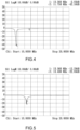
FIG. 4 is a schematic view of the operating frequency of the radio frequency tag module before being covered with a metal foil according to an embodiment of the disclosure. -
FIG. 5 is a schematic view of the operating frequency of the radio frequency tag module after being covered with the metal foil according to an embodiment of the disclosure. - Referring to
FIG. 1 , there is shown a schematic view of a back cover of a laptop according to an embodiment of the disclosure. Aback cover 3 of a back coverheat dissipation structure 1 of a laptop, as provided by the disclosure, comprises aplating region 31 and areceiving chamber 32. Theplating region 31 is a metal film or any other coating with high coefficient of thermal conductivity and is adapted to increase heat dissipation area and achieve heat dissipation. - Referring to
FIG. 2 , there is shown a schematic view of a radio frequency tag module according to an embodiment of the disclosure. A radiofrequency tag module 2 of the back coverheat dissipation structure 1 of a laptop, as provided by the disclosure, comprises acircuit board 23 with acomponent region 21 and anantenna region 22. Thecomponent region 21 and theantenna region 22 are disposed on the bottom side and the top side of thecircuit board 23, respectively. - Referring to
FIG. 3 , there is shown a schematic view of the back cover heat dissipation structure of a laptop according to an embodiment of the disclosure. The back coverheat dissipation structure 1 of a laptop, as provided by the disclosure, comprises the radiofrequency tag module 2, theback cover 3, and ametal foil 4. Thereceiving chamber 32 of theback cover 3 receives the radiofrequency tag module 2. The top side of thecircuit board 23 of the radiofrequency tag module 2 is attached to the bottom of thereceiving chamber 32. Themetal foil 4, exemplified by aluminum foil, not only covers the bottom side of thecircuit board 23 of the radiofrequency tag module 2, but also extends to cover theplating region 31 of theback cover 3, so as to increase heat dissipation area and achieve heat dissipation. - When the
metal foil 4 covers the radiofrequency tag module 2, themetal foil 4 causes impedance offset or mismatch to components in thecomponent region 21 on thecircuit board 23. Thus, before the radiofrequency tag module 2 is covered with themetal foil 4, at least one component with offset or mismatched impedance is selected and placed in the component region 21 (for example, at least one resistor-inductor-capacitor (RLC) component with offset or mismatched impedance is selected.) When themetal foil 4 covers the radiofrequency tag module 2, the offset or mismatched impedance of the component is adjusted, such that the operating frequency of the radiofrequency tag module 2 falls within an appropriate operating frequency range, such as 13 Mhz to 14 MHz, or close to an operating frequency of 13.56 MHz, for example. By contrast, the radiofrequency tag module 2 is not covered with themetal foil 4 not only operates within an offset operating frequency range, such as 11 Mhz to 12 MHz, or approximately at an offset operating frequency of 11.75 MHz, but is also characterized by narrow bandwidth and poor sensing capability, as shown inFIG. 4 . The radiofrequency tag module 2 covered with themetal foil 4 not only can operate at an operating frequency of 13.43 MHz but is also characterized by wide bandwidth and good sensing capability, as shown inFIG. 5 . Therefore, the back coverheat dissipation structure 1 of a laptop, as provided by the disclosure, exhibits optimal sensing capability of the radiofrequency tag module 2 and prevents sensing failure. - Therefore, the back cover
heat dissipation structure 1 of a laptop, as provided by the disclosure, comprises a metal foil which covers the radio frequency tag module and extends to cover a plating region of a back cover, so as to increase the heat dissipation area of all the computer elements, parts and components of the laptop. Furthermore, the impedance of components of the radio frequency tag module is adjusted to optimize the sensing capability of the radio frequency tag module and thereby prevent sensing failure. - Although the disclosure is disclosed above by embodiments, the embodiments are not restrictive of the disclosure. Changes and modifications made by persons skilled in the art to the embodiments without departing from the spirit and scope of the disclosure must be deemed falling within the scope of the claims of the disclosure. Accordingly, the legal protection for the disclosure should be defined by the appended claims.
Claims (8)
- A back cover heat dissipation structure of a laptop, comprising:a radio frequency tag module comprising a circuit board with a component region and an antenna region, wherein the component region and the antenna region are disposed on a bottom side and a top side of the circuit board, respectively;a back cover comprising a plating region and a receiving chamber, wherein the receiving chamber receives the radio frequency tag module, and the top side of the circuit board is attached to a bottom of the receiving chamber; anda metal foil covering the bottom side of the circuit board and extending to cover the plating region.
- The back cover heat dissipation structure of a laptop according to claim 1, wherein the metal foil is aluminum foil.
- The back cover heat dissipation structure of a laptop according to claim 1, wherein the radio frequency tag module not covered with the metal foil operates within an offset operating frequency range.
- The back cover heat dissipation structure of a laptop according to claim 3, wherein the offset operating frequency range is 11 Mhz to 12 MHz.
- The back cover heat dissipation structure of a laptop according to claim 1, wherein the radio frequency tag module covered with the metal foil operates within an operating frequency range.
- The back cover heat dissipation structure of a laptop according to claim 5, wherein the operating frequency range is 13 Mhz to 14 MHz.
- The back cover heat dissipation structure of a laptop according to claim 1, wherein at least one component with mismatched impedance is disposed in the component region.
- The back cover heat dissipation structure of a laptop according to claim 7, wherein the component with mismatched impedance comprises at least one resistor-inductor-capacitor (RLC) component.
Applications Claiming Priority (1)
| Application Number | Priority Date | Filing Date | Title |
|---|---|---|---|
| US202263351425P | 2022-06-12 | 2022-06-12 |
Publications (2)
| Publication Number | Publication Date |
|---|---|
| EP4290682A1 true EP4290682A1 (en) | 2023-12-13 |
| EP4290682B1 EP4290682B1 (en) | 2026-04-15 |
Family
ID=84363024
Family Applications (3)
| Application Number | Title | Priority Date | Filing Date |
|---|---|---|---|
| EP22209637.2A Pending EP4290680A1 (en) | 2022-06-12 | 2022-11-25 | Millimeter wave communication apparatus |
| EP23152667.4A Active EP4290682B1 (en) | 2022-06-12 | 2023-01-20 | Back cover heat dissipation structure of laptop |
| EP23152624.5A Active EP4290681B1 (en) | 2022-06-12 | 2023-01-20 | Wireless signal receiving circuit and system |
Family Applications Before (1)
| Application Number | Title | Priority Date | Filing Date |
|---|---|---|---|
| EP22209637.2A Pending EP4290680A1 (en) | 2022-06-12 | 2022-11-25 | Millimeter wave communication apparatus |
Family Applications After (1)
| Application Number | Title | Priority Date | Filing Date |
|---|---|---|---|
| EP23152624.5A Active EP4290681B1 (en) | 2022-06-12 | 2023-01-20 | Wireless signal receiving circuit and system |
Country Status (5)
| Country | Link |
|---|---|
| US (3) | US12356591B2 (en) |
| EP (3) | EP4290680A1 (en) |
| CN (3) | CN117254242A (en) |
| AU (3) | AU2022279483B2 (en) |
| TW (3) | TWI854339B (en) |
Citations (2)
| Publication number | Priority date | Publication date | Assignee | Title |
|---|---|---|---|---|
| KR20160067321A (en) * | 2014-12-03 | 2016-06-14 | 주식회사 아모그린텍 | Heat dissipation sheet unified antenna and electronic equipment having the same |
| CN206574838U (en) * | 2016-12-19 | 2017-10-20 | 上海德门电子科技有限公司 | A kind of NFC antenna component with heat sinking function |
Family Cites Families (55)
| Publication number | Priority date | Publication date | Assignee | Title |
|---|---|---|---|---|
| US6717801B1 (en) * | 2000-09-29 | 2004-04-06 | Hewlett-Packard Development Company, L.P. | Standardized RF module insert for a portable electronic processing device |
| KR20040020218A (en) * | 2002-08-30 | 2004-03-09 | 주식회사 어필텔레콤 | The performance improvement SAR by grounding board in wireless phone |
| TW200512566A (en) * | 2003-09-19 | 2005-04-01 | Quanta Comp Inc | Concealed antenna used in a notebook |
| US7184617B2 (en) * | 2004-03-12 | 2007-02-27 | Matsushita Electric Industrial Co., Ltd. | Portable device |
| US7376446B2 (en) * | 2004-07-15 | 2008-05-20 | Nokia Siemens Networks Gmbh & Co. Kg | Mobile communications network with expanded carrier capacity and method of expanding base station carrier capacity |
| JP2006065700A (en) * | 2004-08-27 | 2006-03-09 | Ricoh Co Ltd | Wireless communication system. |
| US7212161B2 (en) * | 2004-11-19 | 2007-05-01 | Lenovo (Singapore) Pte. Ltd. | Low-profile embedded antenna architectures for wireless devices |
| US7199762B2 (en) * | 2005-08-24 | 2007-04-03 | Motorola Inc. | Wireless device with distributed load |
| US7512388B2 (en) | 2005-09-22 | 2009-03-31 | Skyworks Solutions, Inc. | Multiband or multimode front end antenna switch |
| JP4216865B2 (en) * | 2006-05-29 | 2009-01-28 | 株式会社東芝 | Information equipment that can communicate |
| US8295899B2 (en) * | 2006-09-21 | 2012-10-23 | Kyocera Corporation | Mobile wireless device with an inductive coupler |
| US7733276B2 (en) * | 2006-11-09 | 2010-06-08 | Intel Corporation | Antenna system for notebook computer and method for communicating in multiple wireless systems |
| JP4970226B2 (en) * | 2006-12-05 | 2012-07-04 | パナソニック株式会社 | ANTENNA DEVICE AND WIRELESS COMMUNICATION DEVICE |
| JP4804447B2 (en) * | 2006-12-05 | 2011-11-02 | パナソニック株式会社 | ANTENNA DEVICE AND WIRELESS COMMUNICATION DEVICE |
| JP4571988B2 (en) * | 2007-01-19 | 2010-10-27 | パナソニック株式会社 | Array antenna device and wireless communication device |
| JP4973311B2 (en) * | 2007-05-16 | 2012-07-11 | ソニー株式会社 | Electronics |
| JP2009296377A (en) * | 2008-06-05 | 2009-12-17 | Toshiba Corp | Electronic apparatus |
| TWI405365B (en) * | 2009-05-14 | 2013-08-11 | Wistron Corp | Electronic apparatus and antenna module thereof |
| US20110194240A1 (en) * | 2010-02-05 | 2011-08-11 | Broadcom Corporation | Waveguide assembly and applications thereof |
| JP5565858B2 (en) * | 2010-04-26 | 2014-08-06 | Necカシオモバイルコミュニケーションズ株式会社 | Mobile communication terminal |
| KR20130006820A (en) | 2011-06-24 | 2013-01-18 | 삼성전자주식회사 | Cradle for portable terminal |
| TW201312852A (en) * | 2011-09-15 | 2013-03-16 | Acer Inc | System for antenna extension and method thereof |
| US8988294B2 (en) * | 2011-12-06 | 2015-03-24 | Viasat, Inc. | Antenna with integrated condensation control system |
| CN103326103B (en) * | 2012-03-23 | 2015-07-29 | 联想(北京)有限公司 | There is the electronic equipment of embedded antenna |
| US9048959B2 (en) * | 2012-09-21 | 2015-06-02 | Nokia Corporation | Method and apparatus for a wireless optical link |
| US9660336B2 (en) * | 2013-02-07 | 2017-05-23 | Kevan ANDERSON | Systems, devices and methods for transmitting electrical signals through a faraday cage |
| US9306259B2 (en) * | 2013-03-19 | 2016-04-05 | Texas Instruments Incorporated | Horn antenna for launching electromagnetic signal from microstrip to dielectric waveguide |
| US8954122B2 (en) * | 2013-07-03 | 2015-02-10 | BluFlux RF Technologies, LLC | Electronic device case with antenna |
| TWI552430B (en) * | 2013-09-26 | 2016-10-01 | 財團法人工業技術研究院 | Connector, antenna and electronic device |
| US9331835B1 (en) * | 2014-03-19 | 2016-05-03 | Amazon Technologies, Inc. | Radio frequency (RF) front-end circuitry for wireless local area network (WLAN), wide area network (WAN) and global positioning system (GPS) communications |
| US9786981B2 (en) * | 2014-07-15 | 2017-10-10 | Microsoft Technology Licensing, Llc | Antenna for electronic device |
| US9484631B1 (en) * | 2014-12-01 | 2016-11-01 | Amazon Technologies, Inc. | Split band antenna design |
| WO2016137518A1 (en) * | 2015-02-27 | 2016-09-01 | Hewlett-Packard Development Company, L.P. | Waveguides in a computing device |
| WO2016147695A1 (en) * | 2015-03-17 | 2016-09-22 | ソニー株式会社 | Connector device and communication system |
| JP6549437B2 (en) * | 2015-07-22 | 2019-07-24 | デクセリアルズ株式会社 | Antenna device and electronic device |
| JP6526509B2 (en) * | 2015-07-23 | 2019-06-05 | 株式会社東芝 | Waveguide bend and radio equipment |
| DE102016102073A1 (en) * | 2016-02-05 | 2017-08-10 | Snaptrack, Inc. | Front-end module for carrier aggregation operation |
| WO2017137224A1 (en) * | 2016-02-12 | 2017-08-17 | Telefonaktiebolaget Lm Ericsson (Publ) | A transition arrangement comprising a contactless transition or connection between an siw and a waveguide or an antenna |
| US10431874B2 (en) * | 2016-02-19 | 2019-10-01 | Samsung Electronics Co., Ltd. | Antenna device and electronic device including the same |
| US10075199B2 (en) | 2016-07-17 | 2018-09-11 | Skyworks Solutions, Inc. | Uplink carrier aggregation front-end architecture that supports simultaneous MIMO |
| WO2018044916A1 (en) * | 2016-08-29 | 2018-03-08 | Skyworks Solutions, Inc. | Multi-standard radio switchable multiplexer |
| US10117355B2 (en) * | 2016-08-29 | 2018-10-30 | Chemnova Technologies, Inc. | Heat dissipation foil and methods of heat dissipation |
| US10673484B2 (en) | 2017-05-12 | 2020-06-02 | Qualcomm Incorporated | Antenna diversity switching |
| US10490511B2 (en) * | 2017-06-01 | 2019-11-26 | Mediatek Inc. | Microelectronic assembly with electromagnetic shielding |
| KR102723240B1 (en) | 2017-12-07 | 2024-10-31 | 인피니언 테크놀로지스 아게 | System and method for a radio frequency filter |
| US11158957B1 (en) | 2018-03-07 | 2021-10-26 | Hewlett-Packard Development Company, L.P. | Co-located antennas with coupled arms |
| US11411615B2 (en) | 2018-03-29 | 2022-08-09 | Qualcomm Incorporated | Enhanced antenna utilization |
| KR102658531B1 (en) * | 2019-05-15 | 2024-04-18 | 삼성전자주식회사 | Method for mutiple bands communication using single antenna and electronic device thereof |
| US10990136B2 (en) | 2019-08-12 | 2021-04-27 | Htc Corporation | Wireless communication device and case assembly |
| KR102648537B1 (en) * | 2019-09-19 | 2024-03-18 | 삼성전자주식회사 | An electronic device including an antenna module in which a heat transfer member is extended |
| WO2021095255A1 (en) * | 2019-11-15 | 2021-05-20 | ソニーグループ株式会社 | Portable electronic device |
| TWM596462U (en) * | 2020-01-17 | 2020-06-01 | 華碩電腦股份有限公司 | Rotary antenna module and electronic device thereof |
| CN111430921B (en) * | 2020-03-31 | 2024-03-01 | 北京小米移动软件有限公司 | Ultra wideband antenna and communication terminal |
| KR102738877B1 (en) * | 2020-06-05 | 2024-12-06 | 삼성전자주식회사 | Antenna filter and electronic device inlcuding the same |
| US12126067B2 (en) * | 2020-06-25 | 2024-10-22 | Intel Corporation | Millimeter-wave dielectric waveguide including an opening of varying cross-section enclosed within a first material and the first material surrounded by a second material |
-
2022
- 2022-10-28 TW TW111141263A patent/TWI854339B/en active
- 2022-10-28 TW TW111141262A patent/TWI904390B/en active
- 2022-10-28 CN CN202211337276.XA patent/CN117254242A/en active Pending
- 2022-10-28 CN CN202211338148.7A patent/CN117251032A/en active Pending
- 2022-11-03 US US17/980,494 patent/US12356591B2/en active Active
- 2022-11-25 EP EP22209637.2A patent/EP4290680A1/en active Pending
- 2022-11-30 AU AU2022279483A patent/AU2022279483B2/en active Active
-
2023
- 2023-01-13 US US18/097,158 patent/US12178018B2/en active Active
- 2023-01-18 US US18/098,648 patent/US12369280B2/en active Active
- 2023-01-20 EP EP23152667.4A patent/EP4290682B1/en active Active
- 2023-01-20 EP EP23152624.5A patent/EP4290681B1/en active Active
- 2023-02-07 AU AU2023200637A patent/AU2023200637B2/en active Active
- 2023-02-07 AU AU2023200639A patent/AU2023200639B1/en active Active
- 2023-02-16 CN CN202310121890.0A patent/CN117220702A/en active Pending
- 2023-02-16 TW TW112105583A patent/TWI854488B/en active
Patent Citations (2)
| Publication number | Priority date | Publication date | Assignee | Title |
|---|---|---|---|---|
| KR20160067321A (en) * | 2014-12-03 | 2016-06-14 | 주식회사 아모그린텍 | Heat dissipation sheet unified antenna and electronic equipment having the same |
| CN206574838U (en) * | 2016-12-19 | 2017-10-20 | 上海德门电子科技有限公司 | A kind of NFC antenna component with heat sinking function |
Also Published As
| Publication number | Publication date |
|---|---|
| AU2023200637B2 (en) | 2024-07-25 |
| CN117220702A (en) | 2023-12-12 |
| EP4290682B1 (en) | 2026-04-15 |
| CN117251032A (en) | 2023-12-19 |
| CN117254242A (en) | 2023-12-19 |
| TW202350059A (en) | 2023-12-16 |
| EP4290680A1 (en) | 2023-12-13 |
| TW202349790A (en) | 2023-12-16 |
| AU2022279483B2 (en) | 2024-06-13 |
| AU2023200639B1 (en) | 2024-01-25 |
| EP4290681B1 (en) | 2025-12-17 |
| TWI854339B (en) | 2024-09-01 |
| EP4290681A1 (en) | 2023-12-13 |
| US12356591B2 (en) | 2025-07-08 |
| AU2022279483A1 (en) | 2024-01-18 |
| US12369280B2 (en) | 2025-07-22 |
| TWI904390B (en) | 2025-11-11 |
| US20230403046A1 (en) | 2023-12-14 |
| TWI854488B (en) | 2024-09-01 |
| US20230400898A1 (en) | 2023-12-14 |
| US20230403034A1 (en) | 2023-12-14 |
| AU2023200637A1 (en) | 2024-01-18 |
| TW202349890A (en) | 2023-12-16 |
| US12178018B2 (en) | 2024-12-24 |
Similar Documents
| Publication | Publication Date | Title |
|---|---|---|
| US9894748B2 (en) | Electronic device | |
| EP3125038B1 (en) | Camera module and manufacturing method therefor | |
| US10411333B1 (en) | Electronic device | |
| US20090207578A1 (en) | Apparatus for reducing electromagnetic interference and spreading heat | |
| US7671811B2 (en) | Antenna device with ground plane coupled to conductive portion of an electronic device | |
| US11121450B1 (en) | Electronic apparatus | |
| US20070236397A1 (en) | Antenna device with antenna element coupled to anti-EMI plate of an electronic device | |
| US12178018B2 (en) | Back cover heat dissipation structure of laptop | |
| US11460891B2 (en) | Electronic device | |
| CN210183794U (en) | Electronic device | |
| US20160273564A1 (en) | Sub-flush circuit board mounting screw | |
| US10177441B2 (en) | Antenna module | |
| US9480191B2 (en) | Electronic apparatus having integrated shielding film | |
| US20110019369A1 (en) | Electronic circuit module with good heat dissipation | |
| US11757173B2 (en) | Electronic display device | |
| US7782622B1 (en) | Attachment apparatus for electronic boards | |
| TWI403025B (en) | Integrated antenna for worldwide interoperability for microwave access (wimax) and wlan | |
| US11011855B2 (en) | Antenna system | |
| US20240313407A1 (en) | Antenna structure | |
| US10706832B2 (en) | Noise reduction device and printed circuit assembly including the same | |
| US20050185380A1 (en) | Dissipation structure and method for backlight inverter | |
| CN113885678B (en) | Radiating assembly and notebook computer with same | |
| US20250192433A1 (en) | Electronic device and antenna structure | |
| US10903564B2 (en) | Communication apparatus | |
| CN223067383U (en) | Spring plate device for shielding radio frequency noise and heat dissipation shielding assembly |
Legal Events
| Date | Code | Title | Description |
|---|---|---|---|
| PUAI | Public reference made under article 153(3) epc to a published international application that has entered the european phase |
Free format text: ORIGINAL CODE: 0009012 |
|
| STAA | Information on the status of an ep patent application or granted ep patent |
Free format text: STATUS: THE APPLICATION HAS BEEN PUBLISHED |
|
| AK | Designated contracting states |
Kind code of ref document: A1 Designated state(s): AL AT BE BG CH CY CZ DE DK EE ES FI FR GB GR HR HU IE IS IT LI LT LU LV MC ME MK MT NL NO PL PT RO RS SE SI SK SM TR |
|
| STAA | Information on the status of an ep patent application or granted ep patent |
Free format text: STATUS: REQUEST FOR EXAMINATION WAS MADE |
|
| 17P | Request for examination filed |
Effective date: 20240220 |
|
| RBV | Designated contracting states (corrected) |
Designated state(s): AL AT BE BG CH CY CZ DE DK EE ES FI FR GB GR HR HU IE IS IT LI LT LU LV MC ME MK MT NL NO PL PT RO RS SE SI SK SM TR |
|
| GRAJ | Information related to disapproval of communication of intention to grant by the applicant or resumption of examination proceedings by the epo deleted |
Free format text: ORIGINAL CODE: EPIDOSDIGR1 |
|
| GRAP | Despatch of communication of intention to grant a patent |
Free format text: ORIGINAL CODE: EPIDOSNIGR1 |
|
| GRAP | Despatch of communication of intention to grant a patent |
Free format text: ORIGINAL CODE: EPIDOSNIGR1 |
|
| STAA | Information on the status of an ep patent application or granted ep patent |
Free format text: STATUS: GRANT OF PATENT IS INTENDED |
|
| RIC1 | Information provided on ipc code assigned before grant |
Ipc: H01Q 1/22 20060101AFI20251127BHEP Ipc: G06F 1/16 20060101ALI20251127BHEP Ipc: H01Q 1/24 20060101ALI20251127BHEP Ipc: H01Q 5/50 20150101ALI20251127BHEP Ipc: H04B 1/40 20150101ALI20251127BHEP Ipc: H04M 1/04 20060101ALI20251127BHEP Ipc: H04M 1/72409 20210101ALN20251127BHEP |
|
| RIC1 | Information provided on ipc code assigned before grant |
Ipc: H01Q 1/22 20060101AFI20251204BHEP Ipc: G06F 1/16 20060101ALI20251204BHEP Ipc: H01Q 1/24 20060101ALI20251204BHEP Ipc: H01Q 5/50 20150101ALI20251204BHEP Ipc: H04B 1/40 20150101ALI20251204BHEP Ipc: H04M 1/04 20060101ALI20251204BHEP Ipc: H04M 1/72409 20210101ALN20251204BHEP |
|
| INTG | Intention to grant announced |
Effective date: 20251212 |
|
| GRAS | Grant fee paid |
Free format text: ORIGINAL CODE: EPIDOSNIGR3 |
|
| GRAA | (expected) grant |
Free format text: ORIGINAL CODE: 0009210 |
|
| STAA | Information on the status of an ep patent application or granted ep patent |
Free format text: STATUS: THE PATENT HAS BEEN GRANTED |
|
| AK | Designated contracting states |
Kind code of ref document: B1 Designated state(s): AL AT BE BG CH CY CZ DE DK EE ES FI FR GB GR HR HU IE IS IT LI LT LU LV MC ME MK MT NL NO PL PT RO RS SE SI SK SM TR |
|
| REG | Reference to a national code |
Ref country code: CH Ref legal event code: F10 Free format text: ST27 STATUS EVENT CODE: U-0-0-F10-F00 (AS PROVIDED BY THE NATIONAL OFFICE) Effective date: 20260415 |
|
| REG | Reference to a national code |
Ref country code: DE Ref legal event code: R096 Ref document number: 602023015130 Country of ref document: DE |