EP4290518A1 - Calibration control circuit, electronic device and calibration control method - Google Patents
Calibration control circuit, electronic device and calibration control method Download PDFInfo
- Publication number
- EP4290518A1 EP4290518A1 EP22738527.5A EP22738527A EP4290518A1 EP 4290518 A1 EP4290518 A1 EP 4290518A1 EP 22738527 A EP22738527 A EP 22738527A EP 4290518 A1 EP4290518 A1 EP 4290518A1
- Authority
- EP
- European Patent Office
- Prior art keywords
- calibration
- chip
- code
- module
- mode
- Prior art date
- Legal status (The legal status is an assumption and is not a legal conclusion. Google has not performed a legal analysis and makes no representation as to the accuracy of the status listed.)
- Granted
Links
Images

Classifications
-
- B—PERFORMING OPERATIONS; TRANSPORTING
- B60—VEHICLES IN GENERAL
- B60K—ARRANGEMENT OR MOUNTING OF PROPULSION UNITS OR OF TRANSMISSIONS IN VEHICLES; ARRANGEMENT OR MOUNTING OF PLURAL DIVERSE PRIME-MOVERS IN VEHICLES; AUXILIARY DRIVES FOR VEHICLES; INSTRUMENTATION OR DASHBOARDS FOR VEHICLES; ARRANGEMENTS IN CONNECTION WITH COOLING, AIR INTAKE, GAS EXHAUST OR FUEL SUPPLY OF PROPULSION UNITS IN VEHICLES
- B60K17/00—Arrangement or mounting of transmissions in vehicles
- B60K17/04—Arrangement or mounting of transmissions in vehicles characterised by arrangement, location or kind of gearing
- B60K17/06—Arrangement or mounting of transmissions in vehicles characterised by arrangement, location or kind of gearing of change-speed gearing
- B60K17/08—Arrangement or mounting of transmissions in vehicles characterised by arrangement, location or kind of gearing of change-speed gearing of mechanical type
-
- G—PHYSICS
- G11—INFORMATION STORAGE
- G11C—STATIC STORES
- G11C7/00—Arrangements for writing information into, or reading information out from, a digital store
- G11C7/10—Input/output [I/O] data interface arrangements, e.g. I/O data control circuits, I/O data buffers
- G11C7/1048—Data bus control circuits, e.g. precharging, presetting, equalising
-
- B—PERFORMING OPERATIONS; TRANSPORTING
- B60—VEHICLES IN GENERAL
- B60K—ARRANGEMENT OR MOUNTING OF PROPULSION UNITS OR OF TRANSMISSIONS IN VEHICLES; ARRANGEMENT OR MOUNTING OF PLURAL DIVERSE PRIME-MOVERS IN VEHICLES; AUXILIARY DRIVES FOR VEHICLES; INSTRUMENTATION OR DASHBOARDS FOR VEHICLES; ARRANGEMENTS IN CONNECTION WITH COOLING, AIR INTAKE, GAS EXHAUST OR FUEL SUPPLY OF PROPULSION UNITS IN VEHICLES
- B60K17/00—Arrangement or mounting of transmissions in vehicles
- B60K17/04—Arrangement or mounting of transmissions in vehicles characterised by arrangement, location or kind of gearing
-
- B—PERFORMING OPERATIONS; TRANSPORTING
- B60—VEHICLES IN GENERAL
- B60K—ARRANGEMENT OR MOUNTING OF PROPULSION UNITS OR OF TRANSMISSIONS IN VEHICLES; ARRANGEMENT OR MOUNTING OF PLURAL DIVERSE PRIME-MOVERS IN VEHICLES; AUXILIARY DRIVES FOR VEHICLES; INSTRUMENTATION OR DASHBOARDS FOR VEHICLES; ARRANGEMENTS IN CONNECTION WITH COOLING, AIR INTAKE, GAS EXHAUST OR FUEL SUPPLY OF PROPULSION UNITS IN VEHICLES
- B60K1/00—Arrangement or mounting of electrical propulsion units
- B60K1/02—Arrangement or mounting of electrical propulsion units comprising more than one electric motor
-
- B—PERFORMING OPERATIONS; TRANSPORTING
- B60—VEHICLES IN GENERAL
- B60L—PROPULSION OF ELECTRICALLY-PROPELLED VEHICLES; SUPPLYING ELECTRIC POWER FOR AUXILIARY EQUIPMENT OF ELECTRICALLY-PROPELLED VEHICLES; ELECTRODYNAMIC BRAKE SYSTEMS FOR VEHICLES IN GENERAL; MAGNETIC SUSPENSION OR LEVITATION FOR VEHICLES; MONITORING OPERATING VARIABLES OF ELECTRICALLY-PROPELLED VEHICLES; ELECTRIC SAFETY DEVICES FOR ELECTRICALLY-PROPELLED VEHICLES
- B60L15/00—Methods, circuits, or devices for controlling the traction-motor speed of electrically-propelled vehicles
- B60L15/007—Physical arrangements or structures of drive train converters specially adapted for the propulsion motors of electric vehicles
-
- G—PHYSICS
- G11—INFORMATION STORAGE
- G11C—STATIC STORES
- G11C11/00—Digital stores characterised by the use of particular electric or magnetic storage elements; Storage elements therefor
- G11C11/21—Digital stores characterised by the use of particular electric or magnetic storage elements; Storage elements therefor using electric elements
- G11C11/34—Digital stores characterised by the use of particular electric or magnetic storage elements; Storage elements therefor using electric elements using semiconductor devices
- G11C11/40—Digital stores characterised by the use of particular electric or magnetic storage elements; Storage elements therefor using electric elements using semiconductor devices using transistors
- G11C11/401—Digital stores characterised by the use of particular electric or magnetic storage elements; Storage elements therefor using electric elements using semiconductor devices using transistors forming cells needing refreshing or charge regeneration, i.e. dynamic cells
- G11C11/4063—Auxiliary circuits, e.g. for addressing, decoding, driving, writing, sensing or timing
- G11C11/407—Auxiliary circuits, e.g. for addressing, decoding, driving, writing, sensing or timing for memory cells of the field-effect type
- G11C11/409—Read-write [R-W] circuits
- G11C11/4093—Input/output [I/O] data interface arrangements, e.g. data buffers
-
- G—PHYSICS
- G11—INFORMATION STORAGE
- G11C—STATIC STORES
- G11C29/00—Checking stores for correct operation ; Subsequent repair; Testing stores during standby or offline operation
- G11C29/02—Detection or location of defective auxiliary circuits, e.g. defective refresh counters
- G11C29/028—Detection or location of defective auxiliary circuits, e.g. defective refresh counters with adaption or trimming of parameters
-
- G—PHYSICS
- G11—INFORMATION STORAGE
- G11C—STATIC STORES
- G11C29/00—Checking stores for correct operation ; Subsequent repair; Testing stores during standby or offline operation
- G11C29/04—Detection or location of defective memory elements, e.g. cell constructio details, timing of test signals
- G11C29/50—Marginal testing, e.g. race, voltage or current testing
- G11C29/50008—Marginal testing, e.g. race, voltage or current testing of impedance
-
- B—PERFORMING OPERATIONS; TRANSPORTING
- B60—VEHICLES IN GENERAL
- B60Y—INDEXING SCHEME RELATING TO ASPECTS CROSS-CUTTING VEHICLE TECHNOLOGY
- B60Y2200/00—Type of vehicle
- B60Y2200/90—Vehicles comprising electric prime movers
- B60Y2200/91—Electric vehicles
-
- G—PHYSICS
- G11—INFORMATION STORAGE
- G11C—STATIC STORES
- G11C7/00—Arrangements for writing information into, or reading information out from, a digital store
- G11C7/10—Input/output [I/O] data interface arrangements, e.g. I/O data control circuits, I/O data buffers
- G11C7/1051—Data output circuits, e.g. read-out amplifiers, data output buffers, data output registers, data output level conversion circuits
- G11C7/1057—Data output buffers, e.g. comprising level conversion circuits, circuits for adapting load
-
- Y—GENERAL TAGGING OF NEW TECHNOLOGICAL DEVELOPMENTS; GENERAL TAGGING OF CROSS-SECTIONAL TECHNOLOGIES SPANNING OVER SEVERAL SECTIONS OF THE IPC; TECHNICAL SUBJECTS COVERED BY FORMER USPC CROSS-REFERENCE ART COLLECTIONS [XRACs] AND DIGESTS
- Y02—TECHNOLOGIES OR APPLICATIONS FOR MITIGATION OR ADAPTATION AGAINST CLIMATE CHANGE
- Y02T—CLIMATE CHANGE MITIGATION TECHNOLOGIES RELATED TO TRANSPORTATION
- Y02T10/00—Road transport of goods or passengers
- Y02T10/60—Other road transportation technologies with climate change mitigation effect
- Y02T10/64—Electric machine technologies in electromobility
Definitions
- the present disclosure relates to the technical field of semiconductor memory, and in particular, to a circuit for controlling calibration, an electronic device and a method for controlling calibration.
- a Dynamic Random Access Memory there are an output drive module and a termination resistance module, which are used to implement the signal transmission process.
- a termination resistance module which are used to implement the signal transmission process.
- ZQ calibration it is necessary to calibrate the relevant resistance values of the output drive module and the termination resistance module to match the actual working conditions (such as voltage and temperature), which is called ZQ calibration.
- ZQ calibration a certain amount of power consumption and system time is occupied by ZQ calibration, and the performance of the memory is reduced.
- the present disclosure provides a circuit for controlling calibration, an electronic device and a method for controlling calibration, which can reduce the power consumption of the ZQ calibration process and save the resources of the memory.
- the off-chip calibration module is configured to receive and store a first calibration code sent by a user.
- the on-chip calibration module is configured to receive an enable signal, and perform a ZQ self-calibration process on the memory to obtain a second calibration code adapted to a current environmental parameter in a case that the enable signal is in an active state.
- the second selection module is configured to receive the selection signal, and output the first calibration code as the ZQ calibration code in a case that the selection signal is in the first state, or, output the second calibration code as the ZQ calibration code in a case that the selection signal is in the second state.
- the first selection module is further configured to output the enable signal in the active state to the on-chip calibration module in a case that the calibration mode signal indicates the on-chip calibration mode, or, output the enable signal in an inactive state to the on-chip calibration module in a case that the calibration mode signal indicates the off-chip calibration mode.
- the acquisition module includes a read-only register group, and an input end of the read-only register group is connected to the output end of the multiplexer.
- the read-only register group is configured to acquire an output signal of the multiplexer.
- the read-only register group is further configured to receive, in the test mode and after the on-chip calibration module performs one time of the ZQ self-calibration process, a read command; and output a corresponding candidate calibration code according to the read command.
- the memory further includes an output drive module and a termination resistance module.
- the memory is further configured to write the ZQ calibration code into the output driving module and the termination resistance module to implement a resistance value calibration process of the output drive module and the termination resistance module.
- the embodiments of the present disclosure provide a method for controlling calibration.
- the method is applicable for an electronic device including a memory.
- the method includes the following operations.
- the memory is controlled to perform a ZQ self-calibration process to obtain a second calibration code adapted to a current environmental parameter, and the second calibration code is determined as the ZQ calibration code.
- the method further includes the following operations.
- An enable signal in an inactive state and a selection signal in a first state are determined according to the calibration mode signal.
- the memory is controlled to stop the ZQ self-calibration process by using the enable signal in the inactive state.
- the first calibration code is determined as the ZQ calibration code by using the selection signal in the first state.
- the method further includes the following operations.
- An enable signal in an active state and a selection signal in a second state are determined according to the calibration mode signal.
- the memory is controlled to perform the ZQ self-calibration process by using the enable signal in the active state.
- the second calibration code is determined as the ZQ calibration code by using the selection signal in the second state.
- the method further includes the following operations.
- a current environmental parameter of the memory is detected.
- the current environmental parameter is presented to the user, so that the user selects the first calibration code from multiple candidate calibration codes according to a preset mapping relationship.
- the preset mapping relationship indicates relationships between multiple environmental parameters and the multiple candidate calibration codes, and each multiple environmental parameter includes a voltage parameter and/or a temperature parameter.
- the method further includes the following operations.
- the calibration mode signal is controlled to indicate the on-chip calibration mode.
- the memory is controlled to perform, based on the multiple environmental parameters, the ZQ self-calibration process for multiple times respectively to obtain the multiple candidate calibration codes to establish the preset mapping relationship.
- the method further includes the following operations.
- the first calibration code is stored in a case that the calibration mode signal indicates the on-chip calibration mode and the first calibration code sent by the user is received.
- the first calibration code is determined as the ZQ calibration code after the calibration mode signal is adjusted to indicate the off-chip calibration mode.
- the received first calibration code is determined as the ZQ calibration code directly in a case that the calibration mode signal indicates an off-chip calibration mode and the first calibration code sent by a user is received.
- the method further includes the following operation.
- a resistance value calibration process is performed on an output drive module in the memory and a termination resistance module in the memory based on the ZQ calibration code.
- the embodiments of the present disclosure provide a circuit for controlling calibration, an electronic device and a method for controlling calibration, which allow a user to select an on-chip calibration mode or an off-chip calibration mode to determine the ZQ calibration code, so as to implement the best performance in different practical application scenarios.
- the user may set the ZQ calibration code through the off-chip calibration mode, which can reduce power consumption, save system time, and avoid the deviations for the ZQ calibration code introduced by environmental noise and the degradation of the signal integrity of the memory.
- first ⁇ second ⁇ third involved in the embodiments of the present disclosure is only used to distinguish similar objects, and does not represent a specific ordering of objects. It may be understood that the "first ⁇ second ⁇ third” may be interchanged with a specific order or order of precedence if permitted, so that the embodiments of the present disclosure described herein can be implemented in an order other than those illustrated or described herein.
- the data processing frequency of a memory is getting higher and higher, and maintaining signal integrity during data transmission is a very important task.
- the LPDDR has a ZQ pin (BALL), and the ZQ pin is connected to a reference resistance of 240 ohms externally to calibrate the output impedance of the data signal DQ and the termination impedance of the command address signal CA, so as to implement impedance matching during signal transmission.
- the above impedance calibration process is also called as ZQ calibration.
- the embodiments of the present disclosure provide a circuit for controlling calibration, which allows a user to select an on-chip calibration mode or an off-chip calibration mode to determine the ZQ calibration code, so as to implement the best performance in different practical application scenarios.
- the user may set the ZQ calibration code through the off-chip calibration mode, and the frequent ZQ self-calibration process is not needed, which not only reduces power consumption but also saves system time, thereby reducing resource waste and improving data process performance of memory.
- the deviation introduced by environmental noise to the ZQ calibration code and the degradation of signal integrity of the memory due to impedance mismatch can be avoided through the off-chip calibration mode.
- the off-chip calibration module 11 is configured to receive and store a first calibration code sent by a user.
- the on-chip calibration module 12 is configured to receive an enable signal and perform a ZQ self-calibration process on the memory to obtain a second calibration code adapted to a current environmental parameter in a case that the enable signal is in an active state.
- the mode switching module 13 is configured to receive a calibration mode signal, the first calibration code and the second calibration code, and determine the first calibration code as a ZQ calibration code in the case that the calibration mode signal indicates an off-chip calibration mode, or, determine the second calibration code as the ZQ calibration code in a case that the calibration mode signal indicates an on-chip calibration mode.
- two different modes are provided by the memory to implement ZQ calibration, i.e., an off-chip calibration mode and an on-chip calibration mode.
- the off-chip calibration mode the user may set the ZQ calibration code directly.
- the ZQ calibration code is obtained by performing ZQ self-calibration process on the memory. It should be understood that the ZQ calibration code is subsequently used to be written into the input impedance module and the termination resistance module, so as to calibrate the output impedance of the data signal DQ and the termination impedance of the command address signal CA to expected values.
- the on-chip calibration module 12 is connected to a standard resistance (resistance value is 240 ohms) externally, and the on-chip calibration module 12 can perform ZQ self-calibration process based on the standard resistance, and calibrate the output impedance and termination impedance of the memory to the standard resistance value.
- the ZQ self-calibration process refers to the on-chip ZQ calibration that is automatically performed under the condition limitations of certain changes in temperature, voltage, and time. For details, the reference is made to the relevant regulations of JEDEC. Elaborations are omitted herein.
- the user is allowed to select the on-chip calibration mode or the off-chip calibration mode to determine the ZQ calibration code, so as to implement the best performance in different practical application scenarios.
- the user may set the ZQ calibration code through the off-chip calibration mode directly, and the frequent ZQ self-calibration process is not needed, which not only reduces power consumption but also saves system time, thereby reducing resource waste and improving data process performance of memory.
- the deviation introduced by environmental noise to the ZQ calibration code and the degradation of signal integrity of the memory due to impedance mismatch can be avoided through the off-chip calibration mode.
- the first selection module 131 is configured to receive the calibration mode signal, and output a selection signal in a first state in a case that the calibration mode signal indicates the off-chip calibration mode, or, output a selection signal in a second state in a case that the calibration mode signal indicates the on-chip calibration mode.
- the first selection module 131 is further configured to output the enable signal in the active state to the on-chip calibration module in a case that the calibration mode signal indicates the on-chip calibration mode, or, output the enable signal in an inactive state to the on-chip calibration module in a case that the calibration mode signal indicates the off-chip calibration mode.
- the enable signal in the on-chip calibration mode, the enable signal is in an active state, so that the on-chip calibration module 12 performs ZQ self-calibration process on the memory, and a ZQ calibration code adapted to the current environmental parameters can be obtained, the ZQ calibration process without the user's perception is implemented.
- the enable signal In the off-chip calibration mode, the enable signal is in an inactive state, the on-chip calibration module 12 stops to perform the ZQ self-calibration process, which can reduce power consumption, save system time, and avoid introducing environmental noise.
- FIG. 3 a schematic diagram of an application scenario of a circuit for controlling calibration 10 provided by the embodiments of the present disclosure is shown. It may be seen from FIG. 2 and FIG. 3 that, in some embodiments, the first selection module 131 includes a first write-only register 201, the second selection module 132 includes a multiplexer 202, and the off-chip calibration module 11 includes a second write-only register group 203.
- An input end of the first write-only register 201 is used for receiving the calibration mode signal, and an input end of the second write-only register group 203 is used for receiving the first calibration code.
- An enable end of the on-chip calibration module 12 is connected to a first output end of the first write-only register 201 to receive the enable signal.
- the user before switching from the on-chip calibration mode to the off-chip calibration mode, the user should send the first calibration code firstly to avoid a blank interval in the ZQ calibration code after switching from the on-chip calibration mode to the off-chip calibration mode. That is to say, if the user directly switches the on-chip calibration mode to the off-chip calibration mode without sending the first calibration code firstly, there may be no data in the second write-only register group 203 at this time or there may be inappropriate data (for example, data in off-chip calibration mode in the last time) in the second write-only register group 203 at this time, which result in a signal error due to the impedance mismatch of the memory.
- the circuit structure shown in FIG. 3 is not the only choice due to the diversity of circuit elements.
- the first write-only register 201 may have only one output end. If the inactive state of the enable signal is the same as the first state of the calibration mode signal, both the input end of the first write-only register 201 and the enable end of the on-chip calibration module 12 may be connected to the only output end of the first write-only register 201. If the inactive state of the enable signal is different from the first state of the calibration mode signal, the related logic may be implemented with the help of an inverter.
- the mode switching module 13 is further configured to receive the calibration mode signal indicating an on-chip calibration mode in the test mode, to output the multiple candidate calibration codes.
- the acquisition module 14 is configured to acquire the multiple candidate calibration codes to establish a preset mapping relationship.
- the preset mapping relationship indicates relationships between the multiple environmental parameters and the multiple candidate calibration codes.
- the user selects and obtains the first calibration code from the multiple candidate calibration codes based on the preset mapping relationship and a current environment parameter of the memory.
- the result output of the ZQ self-calibration process is implemented through the acquisition module 14, so that the user may know the relevant value of the ZQ calibration code.
- the calibration mode signal indicates the on-chip calibration mode fixedly, so that self-calibration process is performed on the memory under different environmental parameters, multiple candidate calibration codes are obtained, and a preset mapping relationship is established.
- the environmental parameter is used for indicating the external environment in which the memory is located.
- each environmental parameter may include a voltage parameter and/or a temperature parameter.
- each environmental parameter includes the voltage parameter and the temperature parameters
- the test mode may be entered in a fixed stage of system initialization, and the temperature and voltage of the memory are adjusted through the memory controller, then the memory is controlled to perform ZQ self-calibration process, and the calibration result is output through the acquisition module 14, and the candidate calibration code corresponding to the environmental parameter (temperature parameter and voltage parameter) is obtained.
- the above process is repeated under different temperatures and voltages, candidate calibration codes corresponding to different environmental parameters may be obtained, and a preset mapping relationship is also established.
- the system may also include a temperature control device, after entering the test mode, the voltage of the memory is adjusted by the memory controller, and the temperature of the memory is adjusted by the temperature control device.
- the read-only register group 204 is configured to acquire an output signal of the multiplexer 202.
- the read-only register group 204 is further configured to receive, in the test mode and after the on-chip calibration module performs one time of the ZQ self-calibration process, a read command; and output a corresponding candidate calibration code according to the read command.
- the read-only register group 204 needs to store multiple bits of data, which depends on the number of bits of the ZQ calibration code. That is to say, the number of bits of data stored in the second write-only register group 203 is the same with the number of bits of data stored in the read-only register group 204.
- the input end of the read-only register group 204 and the output end of the read-only register group 204 are also connected to the Command Bus. After the read command MRR (Mode Register Read) is received by the read-only register group 204 from the Command Bus, the candidate calibration code is output.
- MRR Mode Register Read
- the calibration result of the on-chip calibration module 12 may be output by means of the read-only register group 204, so that the user may know the ZQ calibration codes corresponding to different environmental parameters to determine an appropriate first calibration code.
- the memory further includes an output drive module 15 and a termination resistance module 16.
- the memory is further configured to write the ZQ calibration code into the output drive module 15 and the termination resistance module 16 to implement a resistance value calibration process of the output drive module 15 and the termination resistance module 16.
- the environmental parameter includes a temperature parameter and a voltage parameter, taking a system composed of a memory controller and a memory as an example, the working process of the above circuit for controlling calibration 10 will be specifically described.
- the memory controller controls the memory to enter the test mode, and the calibration mode signal indicates the on-chip calibration mode at this time.
- the combination of temperature and voltage is scanned by the memory controller, one case of the combination is scanned for each time, and an on-chip ZQ self-calibration process is performed once by using the on-chip calibration module 12.
- the value of the candidate calibration code is read out through the read-only register group 204, and these values are recorded by the user's System on Chip (SOC).
- SOC System on Chip
- the temperature parameter refers to the current temperature for the memory
- the voltage parameter refers to the power supply voltage used by the output drive module and the termination module the memory.
- the current voltage parameter is determined by a Power Management Unit (PMU) in the system
- the current temperature parameter is determined by a Temper Sensor.
- the first calibration code may be determined from Table 1 based on the current voltage parameter and the current temperature parameter.
- the memory After writing the first calibration code into the second write-only register group 203, the memory is controlled to switch to the off-chip calibration mode by sending the calibration mode signal, and then the calibration code is written into the driver of each DQ (output drive module 15) and CA ODT (terminal resistance module 16) by using the ZQ Latch command, and the on-chip ZQ self-calibration processing is prohibited at the same time, which can implement the purpose of saving power and avoid the deviation introduced by environmental noise to the on-chip ZQ self-calibration.
- the circuit for controlling calibration 10 provided by the embodiments of the present disclosure is also compatible with the conventional ZQ calibration mode. That is, in the normal use process of the user, the memory can be controlled to be in the on-chip calibration mode.
- the on-chip calibration module 12 performs on-chip ZQ self-calibration process on the memory according to the regulations of JEDEC under the condition limitation of certain changes in temperature, voltage, and time.
- the second calibration code is written into the driver of each DQ (output drive module 15) and CA ODT (terminal resistance module 16) by using the ZQ Latch command after end of the calibration.
- the embodiments of the present disclosure provide a circuit for controlling calibration 10, which at least includes the following contents: on the one hand, the ZQ calibration code is controlled by the multiplexer to adopt the first calibration code (off-chip value, set by the user) or the second calibration code (on-chip value, obtained by ZQ self-calibration), so as to adapted to different application scenarios. On the other hand, the read-only register group and the second write-only register group are added, so as it is convenient for the user to read out the candidate calibration code and write the first calibration code.
- a user is allowed to select an on-chip calibration mode or an off-chip calibration mode to determine the ZQ calibration code, so as to implement the best performance in different practical application scenarios.
- the user may set the ZQ calibration code through the off-chip calibration mode, and it is not necessary to preform frequent ZQ self-calibration process, which not only reduces power consumption but also saves system time, thereby reducing resource waste and improving data process performance of memory.
- the deviation introduced by environmental noise to the ZQ calibration code and the degradation of signal integrity of the memory due to impedance mismatch can be avoided through the off-chip calibration mode.
- FIG. 4 a schematic structural diagram of an electronic device provided by the embodiments of the present disclosure is shown.
- the electronic device includes a memory 301, and the memory 301 includes the aforementioned circuit for controlling calibration 10.
- the circuit 10 for controlling calibration exists in the electronic device, a user is allowed to select an on-chip calibration mode or an off-chip calibration mode to determine the ZQ calibration code, so as to implement the best performance in different practical application scenarios.
- the user may set the ZQ calibration code through the off-chip calibration mode, which can reduce power consumption, save system time, and avoid the deviation introduced by environmental noise to the ZQ calibration code and the degradation of signal integrity of the memory due to impedance mismatch.
- FIG. 5 a schematic flowchart of a method for controlling calibration provided by the embodiment of the present disclosure is shown. As shown in FIG. 5 , the method includes the following operations.
- a first calibration code sent by a user is determined as a ZQ calibration code in a case that the calibration mode signal indicates the off-chip calibration mode.
- step S403 in a case that the calibration mode signal indicates the on-chip calibration mode, the memory is controlled to perform a ZQ self-calibration process to obtain a second calibration code adapted to a current environmental parameter, and the second calibration code is determined as the ZQ calibration code.
- the first calibration code sent by the user is used as the ZQ calibration code to implement the impedance calibration of the memory
- the second calibration code obtained after the ZQ self-calibration process is used as the ZQ calibration code, so as to implement impedance calibration of memory.
- the user may set the ZQ calibration code through the off-chip calibration mode, and the frequent ZQ self-calibration process is not needed, which not only reduces power consumption but also saves system time, thereby reducing resource waste and improving data process performance of memory.
- the deviation introduced by environmental noise to the ZQ calibration code and the degradation of signal integrity of the memory due to impedance mismatch can be avoided through the off-chip calibration mode.
- the method may further include the following operations.
- An enable signal in an inactive state and a selection signal in a first state are determined according to the calibration mode signal.
- the memory is controlled to stop the ZQ self-calibration process by using the enable signal in the inactive state.
- the first calibration code is determined as the ZQ calibration code by using the selection signal in the first state.
- a current environmental parameter of the memory is detected.
- the current environmental parameter is presented to the user, so that the user selects the first calibration code from multiple candidate calibration codes according to a preset mapping relationship.
- the preset mapping relationship indicates relationships between multiple environmental parameters and the multiple candidate calibration codes, and each of multiple environmental parameters includes a voltage parameter and/or a temperature parameter.
- the method further includes the following operations.
- the calibration mode signal is controlled to indicate the on-chip calibration mode.
- the memory is controlled to perform, based on the multiple environmental parameters, the ZQ self-calibration process for multiple times respectively to obtain the multiple candidate calibration codes to establish the preset mapping relationship.
- the steps performed by the user mentioned in the embodiments of the present disclosure may also be performed by a software program automatically.
- the first calibration code may be directly determined by the electronic device according to the current environment parameter and the preset mapping relationship.
- software programs are highly automated, and creative efforts by those skilled in the art are not required for improvements similar to the above. Therefore, they should also be regarded as the protection scope of the embodiments of the present disclosure.
- the method further includes the following operations.
- the user should send the first calibration code firstly to avoid the impedance mismatch caused by there is no first calibration code or inappropriate first calibration code after the on-chip calibration mode is switched to the off-chip calibration mode.
- the user may still send a new first calibration code to update the ZQ calibration code.
Landscapes
- Engineering & Computer Science (AREA)
- Transportation (AREA)
- Mechanical Engineering (AREA)
- Chemical & Material Sciences (AREA)
- Combustion & Propulsion (AREA)
- Microelectronics & Electronic Packaging (AREA)
- Computer Hardware Design (AREA)
- Power Engineering (AREA)
- Techniques For Improving Reliability Of Storages (AREA)
- Dram (AREA)
Abstract
Description
- The present disclosure is proposed based on
Chinese patent application No. 202210473826.4, filed on April 29, 2022 - The present disclosure relates to the technical field of semiconductor memory, and in particular, to a circuit for controlling calibration, an electronic device and a method for controlling calibration.
- In a Dynamic Random Access Memory (DRAM), there are an output drive module and a termination resistance module, which are used to implement the signal transmission process. During the working process of the DRAM, it is necessary to calibrate the relevant resistance values of the output drive module and the termination resistance module to match the actual working conditions (such as voltage and temperature), which is called ZQ calibration. However, a certain amount of power consumption and system time is occupied by ZQ calibration, and the performance of the memory is reduced.
- The present disclosure provides a circuit for controlling calibration, an electronic device and a method for controlling calibration, which can reduce the power consumption of the ZQ calibration process and save the resources of the memory.
- The technical solutions of the present disclosure are implemented as follows.
- In a first aspect, the embodiments of the present disclosure provide a circuit for controlling calibration. The circuit is applicable for a memory. The circuit includes an off-chip calibration module, an on-chip calibration module and a mode switching module.
- The off-chip calibration module is configured to receive and store a first calibration code sent by a user.
- The on-chip calibration module is configured to receive an enable signal, and perform a ZQ self-calibration process on the memory to obtain a second calibration code adapted to a current environmental parameter in a case that the enable signal is in an active state.
- The mode switching module is configured to receive a calibration mode signal, the first calibration code and the second calibration code, and determine the first calibration code as a ZQ calibration code in the case that the calibration mode signal indicates an off-chip calibration mode, or, determine the second calibration code as the ZQ calibration code in a case that the calibration mode signal indicates an on-chip calibration mode.
- In some embodiments, the mode switching module includes a first selection module and a second selection module. The first selection module is configured to receive the calibration mode signal, and output a selection signal in a first state in a case that the calibration mode signal indicates the off-chip calibration mode, or, output a selection signal in a second state in a case that the calibration mode signal indicates the on-chip calibration mode.
- The second selection module is configured to receive the selection signal, and output the first calibration code as the ZQ calibration code in a case that the selection signal is in the first state, or, output the second calibration code as the ZQ calibration code in a case that the selection signal is in the second state.
- In some embodiments, the first selection module is further configured to output the enable signal in the active state to the on-chip calibration module in a case that the calibration mode signal indicates the on-chip calibration mode, or, output the enable signal in an inactive state to the on-chip calibration module in a case that the calibration mode signal indicates the off-chip calibration mode.
- In some embodiments, the first selection module includes a first write-only register, the second selection module comprises a multiplexer, and the off-chip calibration module includes a second write-only register group. An input end of the first write-only register is used for receiving the calibration mode signal, and an input end of the second write-only register group is used for receiving the first calibration code. An enable end of the on-chip calibration module is connected to a first output end of the first write-only register to receive the enable signal. A control end of the multiplexer is connected to a second output end of the first write-only register to receive the selection signal, a first input end of the multiplexer is connected to an output end of the on-chip calibration module to receive the second calibration code, a second input end of the multiplexer is connected to an output end of the second write-only register group to receive the first calibration code, an output end of the multiplexer is used for outputting the ZQ calibration code.
- In some embodiments, the circuit for controlling calibration further includes an acquisition module. An input end of the acquisition module is connected to an output end of the mode switching module. The on-chip calibration module is further configured to perform the ZQ self-calibration process on the memory for multiple times for multiple environmental parameters in a test mode, to obtain multiple candidate calibration codes. The mode switching module is further configured to receive the calibration mode signal indicating the on-chip calibration mode in the test mode, to output the multiple candidate calibration codes. The acquisition module is configured to acquire the multiple candidate calibration codes to establish a preset mapping relationship, wherein the preset mapping relationship indicates relationships between the multiple environmental parameters and the multiple candidate calibration codes. During a working process of the memory, the user selects and obtains the first calibration code from the multiple candidate calibration codes based on the preset mapping relationship and a current environment parameter of the memory.
- In some embodiments, the acquisition module includes a read-only register group, and an input end of the read-only register group is connected to the output end of the multiplexer. The read-only register group is configured to acquire an output signal of the multiplexer. The read-only register group is further configured to receive, in the test mode and after the on-chip calibration module performs one time of the ZQ self-calibration process, a read command; and output a corresponding candidate calibration code according to the read command.
- In some embodiments, the memory further includes an output drive module and a termination resistance module. The memory is further configured to write the ZQ calibration code into the output driving module and the termination resistance module to implement a resistance value calibration process of the output drive module and the termination resistance module.
- In a second aspect, the embodiments of the present disclosure provide an electronic device. The electronic device includes a memory, and the memory includes the circuit for controlling calibration described in the first aspect.
- In a third aspect, the embodiments of the present disclosure provide a method for controlling calibration. The method is applicable for an electronic device including a memory. The method includes the following operations.
- A calibration mode signal is received.
- A first calibration code sent by a user is determined as a ZQ calibration code in a case that the calibration mode signal indicates the off-chip calibration mode.
- Optionally, in a case that the calibration mode signal indicates the on-chip calibration mode, the memory is controlled to perform a ZQ self-calibration process to obtain a second calibration code adapted to a current environmental parameter, and the second calibration code is determined as the ZQ calibration code.
- In some embodiments, in the case that the calibration mode signal indicates the off-chip calibration mode, the method further includes the following operations.
- An enable signal in an inactive state and a selection signal in a first state are determined according to the calibration mode signal. The memory is controlled to stop the ZQ self-calibration process by using the enable signal in the inactive state. The first calibration code is determined as the ZQ calibration code by using the selection signal in the first state.
- In some embodiments, in the case that the calibration mode signal indicates the on-chip calibration mode, the method further includes the following operations.
- An enable signal in an active state and a selection signal in a second state are determined according to the calibration mode signal. The memory is controlled to perform the ZQ self-calibration process by using the enable signal in the active state. The second calibration code is determined as the ZQ calibration code by using the selection signal in the second state.
- In some embodiments, the method further includes the following operations.
- A current environmental parameter of the memory is detected. The current environmental parameter is presented to the user, so that the user selects the first calibration code from multiple candidate calibration codes according to a preset mapping relationship. The preset mapping relationship indicates relationships between multiple environmental parameters and the multiple candidate calibration codes, and each multiple environmental parameter includes a voltage parameter and/or a temperature parameter.
- In some embodiments, the method further includes the following operations. In the test mode, the calibration mode signal is controlled to indicate the on-chip calibration mode. The memory is controlled to perform, based on the multiple environmental parameters, the ZQ self-calibration process for multiple times respectively to obtain the multiple candidate calibration codes to establish the preset mapping relationship.
- In some embodiments, the method further includes the following operations. The first calibration code is stored in a case that the calibration mode signal indicates the on-chip calibration mode and the first calibration code sent by the user is received. The first calibration code is determined as the ZQ calibration code after the calibration mode signal is adjusted to indicate the off-chip calibration mode. Optionally, the received first calibration code is determined as the ZQ calibration code directly in a case that the calibration mode signal indicates an off-chip calibration mode and the first calibration code sent by a user is received.
- In some embodiments, the method further includes the following operation. A resistance value calibration process is performed on an output drive module in the memory and a termination resistance module in the memory based on the ZQ calibration code.
- The embodiments of the present disclosure provide a circuit for controlling calibration, an electronic device and a method for controlling calibration, which allow a user to select an on-chip calibration mode or an off-chip calibration mode to determine the ZQ calibration code, so as to implement the best performance in different practical application scenarios. In a case that the external conditions remain unchanged, the user may set the ZQ calibration code through the off-chip calibration mode, which can reduce power consumption, save system time, and avoid the deviations for the ZQ calibration code introduced by environmental noise and the degradation of the signal integrity of the memory.
-
-
FIG. 1 is a schematic structural diagram of a circuit of controlling calibration provided by the embodiments of the present disclosure. -
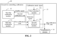
FIG. 2 is a schematic structural diagram of another circuit of controlling calibration provided by the embodiments of the present disclosure. -
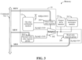
FIG. 3 is a schematic diagram of an application scenario of the circuit of controlling calibration provided by the embodiments of the present disclosure. -
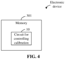
FIG. 4 is a schematic structural diagram of an electronic device provided by the embodiments of the present disclosure. -
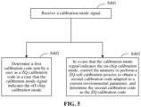
FIG. 5 is a schematic flowchart of a method of controlling calibration provided by the embodiments of the present disclosure. - The technical solutions in the embodiments of the present disclosure will be clearly and completely described below with reference to the accompanying drawings in the embodiments of the present disclosure. It should be understood that the specific embodiments described herein are only used to explain the related disclosure, but not to limit the disclosure. In addition, it should be noted that, for the convenience of description, only the parts related to the relevant disclosure are shown in the drawings.
- Unless otherwise defined, all technical and scientific terms used herein have the same meaning as commonly understood by one of ordinary skill in the art to which the present disclosure belongs. The terminology used herein is for the purpose of describing the embodiments of the present disclosure only and is not intended to limit the present disclosure.
- In the following description, reference is made to "some embodiments" which describe a subset of all possible embodiments, but it is understood that "some embodiments" may be the same or a different subset of all possible embodiments, and may be combined with each other without conflict.
- It should be noted that the term "first\second\third" involved in the embodiments of the present disclosure is only used to distinguish similar objects, and does not represent a specific ordering of objects. It may be understood that the "first\second\third" may be interchanged with a specific order or order of precedence if permitted, so that the embodiments of the present disclosure described herein can be implemented in an order other than those illustrated or described herein.
- The following are the explanations of the professional terms involved in the embodiments of the present disclosure and the corresponding relationship of some nouns.
- Low Power Double Data Rate SDRAM (LPDDR)
- Joint Electron Device Engineering Council (JEDEC)
- With the development of technologies, the data processing frequency of a memory (such as LPDDR) is getting higher and higher, and maintaining signal integrity during data transmission is a very important task. For example, the LPDDR has a ZQ pin (BALL), and the ZQ pin is connected to a reference resistance of 240 ohms externally to calibrate the output impedance of the data signal DQ and the termination impedance of the command address signal CA, so as to implement impedance matching during signal transmission. The above impedance calibration process is also called as ZQ calibration.
- At present, in the working process of the LPDDR, ZQ self-calibration process needs to be performed frequently according to the external conditions where the memory is located. However, if the external conditions are constant, for example, the voltage and temperature are constant, the ZQ calibration code obtained by the same chip after each ZQ calibration is the same roughly, or the lowest bit of the ZQ calibration code is slightly changed by the effect of noise, but it is also within the error range. However, a part of power consumption will be consumed by each ZQ self-calibration process, and a certain calibration time will be taken up, which results in a waste of memory resources. In addition, if the voltage noise of the system is large, the ZQ calibration code may be affected by the voltage noise and be introduced a large deviation. Correspondingly, the signal integrity of the memory will be degraded due to impedance mismatch.
- Based on this, the embodiments of the present disclosure provide a circuit for controlling calibration, which allows a user to select an on-chip calibration mode or an off-chip calibration mode to determine the ZQ calibration code, so as to implement the best performance in different practical application scenarios. In a case that the external conditions remain unchanged, the user may set the ZQ calibration code through the off-chip calibration mode, and the frequent ZQ self-calibration process is not needed, which not only reduces power consumption but also saves system time, thereby reducing resource waste and improving data process performance of memory. In addition, the deviation introduced by environmental noise to the ZQ calibration code and the degradation of signal integrity of the memory due to impedance mismatch can be avoided through the off-chip calibration mode.
- The embodiments of the present disclosure will be described in detail below with reference to the accompanying drawings.
- In an embodiment of the present disclosure, referring to
FIG. 1 , a schematic structural diagram of a circuit for controllingcalibration 10 provided by the embodiments of the present disclosure is shown. As shown inFIG. 1 , the circuit for controllingcalibration 10 includes an off-chip calibration module 11, an on-chip calibration module 12 and amode switching module 13. - The off-
chip calibration module 11 is configured to receive and store a first calibration code sent by a user. - The on-
chip calibration module 12 is configured to receive an enable signal and perform a ZQ self-calibration process on the memory to obtain a second calibration code adapted to a current environmental parameter in a case that the enable signal is in an active state. - The
mode switching module 13 is configured to receive a calibration mode signal, the first calibration code and the second calibration code, and determine the first calibration code as a ZQ calibration code in the case that the calibration mode signal indicates an off-chip calibration mode, or, determine the second calibration code as the ZQ calibration code in a case that the calibration mode signal indicates an on-chip calibration mode. - It should be noted that the
calibration control circuit 10 in the embodiments of the present disclosure is applicable for various types of memories. For example, the memory may be LPDDR4, LPDDR5, DDR4, DDR5, etc. - In the embodiments of the present disclosure, two different modes are provided by the memory to implement ZQ calibration, i.e., an off-chip calibration mode and an on-chip calibration mode. In the off-chip calibration mode, the user may set the ZQ calibration code directly. In the on-chip calibration mode, the ZQ calibration code is obtained by performing ZQ self-calibration process on the memory. It should be understood that the ZQ calibration code is subsequently used to be written into the input impedance module and the termination resistance module, so as to calibrate the output impedance of the data signal DQ and the termination impedance of the command address signal CA to expected values.
- Here, the on-
chip calibration module 12 is connected to a standard resistance (resistance value is 240 ohms) externally, and the on-chip calibration module 12 can perform ZQ self-calibration process based on the standard resistance, and calibrate the output impedance and termination impedance of the memory to the standard resistance value. The ZQ self-calibration process refers to the on-chip ZQ calibration that is automatically performed under the condition limitations of certain changes in temperature, voltage, and time. For details, the reference is made to the relevant regulations of JEDEC. Elaborations are omitted herein. - In this way, in the embodiments of the present disclosure, the user is allowed to select the on-chip calibration mode or the off-chip calibration mode to determine the ZQ calibration code, so as to implement the best performance in different practical application scenarios. In a case that the external conditions remain unchanged, the user may set the ZQ calibration code through the off-chip calibration mode directly, and the frequent ZQ self-calibration process is not needed, which not only reduces power consumption but also saves system time, thereby reducing resource waste and improving data process performance of memory. In addition, the deviation introduced by environmental noise to the ZQ calibration code and the degradation of signal integrity of the memory due to impedance mismatch can be avoided through the off-chip calibration mode.
- As shown in
FIG. 2 , in some embodiments, themode switching module 13 may include afirst selection module 131 and asecond selection module 132. - The
first selection module 131 is configured to receive the calibration mode signal, and output a selection signal in a first state in a case that the calibration mode signal indicates the off-chip calibration mode, or, output a selection signal in a second state in a case that the calibration mode signal indicates the on-chip calibration mode. - The
second selection module 132 is configured to receive the selection signal, and output the first calibration code as the ZQ calibration code in a case that the selection signal is in the first state, or, output the second calibration code as the ZQ calibration code in a case that the selection signal is in the second state. - In some embodiments, the
first selection module 131 is further configured to output the enable signal in the active state to the on-chip calibration module in a case that the calibration mode signal indicates the on-chip calibration mode, or, output the enable signal in an inactive state to the on-chip calibration module in a case that the calibration mode signal indicates the off-chip calibration mode. - It should be understood that the first state and the second state refer to different logic level states, but their specific values may be determined according to practical application scenarios. For example, the first state may be a high-level signal, and the second state may be a low-level signal. Optionally, the first state may be a low-level signal, and the second state may be a high-level signal. Similarly, the active state and the inactive state refer to different logic level states, and their specific values may also be determined according to practical application scenarios, which are not limited in the embodiments of the present disclosure.
- In this way, in the on-chip calibration mode, the enable signal is in an active state, so that the on-
chip calibration module 12 performs ZQ self-calibration process on the memory, and a ZQ calibration code adapted to the current environmental parameters can be obtained, the ZQ calibration process without the user's perception is implemented. In the off-chip calibration mode, the enable signal is in an inactive state, the on-chip calibration module 12 stops to perform the ZQ self-calibration process, which can reduce power consumption, save system time, and avoid introducing environmental noise. - Referring to
FIG. 3 , a schematic diagram of an application scenario of a circuit for controllingcalibration 10 provided by the embodiments of the present disclosure is shown. It may be seen fromFIG. 2 andFIG. 3 that, in some embodiments, thefirst selection module 131 includes a first write-only register 201, thesecond selection module 132 includes amultiplexer 202, and the off-chip calibration module 11 includes a second write-only register group 203. - An input end of the first write-
only register 201 is used for receiving the calibration mode signal, and an input end of the second write-only register group 203 is used for receiving the first calibration code. - An enable end of the on-
chip calibration module 12 is connected to a first output end of the first write-only register 201 to receive the enable signal. - A control end of the
multiplexer 202 is connected to a second output end of the first write-only register 201 and is configured to receive the selection signal. The first input end of themultiplexer 202 is connected to an output end of the on-chip calibration module 12 and is configured to receive the second calibration code ZqAdj2<5:0>. A second input end of themultiplexer 202 is connected to an output end of the second write-only register group 203 and is configured to receive the first calibration code ZqAdj1<5: 0>. The output end of themultiplexer 202 is used for outputting the ZQ calibration code ZqAdj<5:0>. - It should be noted that the first write-
only register 201 may store only one bit of data, and different numerical states (0 or 1) of the data indicate the on-chip calibration mode or the off-chip calibration mode respectively, which depends on the practical application scenario. The second write-only register group 203 needs to store multiple bits of data, which are depended on the number of bits of the ZQ calibration code. Exemplarily, the ZQ calibration code may include 6-bit data, represented as <5:0>. - The input end of the first write-
only register 201 and the input end of the second write-only register group 203 are both connected to a Command Bus, so as to implement related data transmission. Specifically, the user sends the calibration mode signal to the first write-only register 201 in the manner of the write command MRW (Mode Register Write), so that the on -chip calibration mode or the off-chip calibration mode is started. The user sends the first calibration code to the second write-only register group 203 in the manner of the write command MRW, and the first calibration code is used for setting the ZQ calibration code subsequently. - It should be understood that before switching from the on-chip calibration mode to the off-chip calibration mode, the user should send the first calibration code firstly to avoid a blank interval in the ZQ calibration code after switching from the on-chip calibration mode to the off-chip calibration mode. That is to say, if the user directly switches the on-chip calibration mode to the off-chip calibration mode without sending the first calibration code firstly, there may be no data in the second write-
only register group 203 at this time or there may be inappropriate data (for example, data in off-chip calibration mode in the last time) in the second write-only register group 203 at this time, which result in a signal error due to the impedance mismatch of the memory. - It should be noted that, the circuit structure shown in
FIG. 3 is not the only choice due to the diversity of circuit elements. Exemplarily, the first write-only register 201 may have only one output end. If the inactive state of the enable signal is the same as the first state of the calibration mode signal, both the input end of the first write-only register 201 and the enable end of the on-chip calibration module 12 may be connected to the only output end of the first write-only register 201. If the inactive state of the enable signal is different from the first state of the calibration mode signal, the related logic may be implemented with the help of an inverter. - In some embodiments, as shown in
FIG. 2 , the circuit for controllingcalibration 10 further includes anacquisition module 14, and an input end of theacquisition module 14 is connected to an output end of themode switching module 13. - The on-
chip calibration module 12 is further configured to perform the ZQ self-calibration process on the memory for multiple times for multiple environmental parameters in a test mode, to obtain multiple candidate calibration codes. - The
mode switching module 13 is further configured to receive the calibration mode signal indicating an on-chip calibration mode in the test mode, to output the multiple candidate calibration codes. - The
acquisition module 14 is configured to acquire the multiple candidate calibration codes to establish a preset mapping relationship. The preset mapping relationship indicates relationships between the multiple environmental parameters and the multiple candidate calibration codes. - Here, during the working process of the memory, the user selects and obtains the first calibration code from the multiple candidate calibration codes based on the preset mapping relationship and a current environment parameter of the memory.
- It should be noted that, in the embodiments of the present disclosure, the result output of the ZQ self-calibration process is implemented through the
acquisition module 14, so that the user may know the relevant value of the ZQ calibration code. - Specifically, in the test mode, the calibration mode signal indicates the on-chip calibration mode fixedly, so that self-calibration process is performed on the memory under different environmental parameters, multiple candidate calibration codes are obtained, and a preset mapping relationship is established. Here, the environmental parameter is used for indicating the external environment in which the memory is located. Exemplarily, each environmental parameter may include a voltage parameter and/or a temperature parameter.
- It should be noted that, in the case where each environmental parameter includes the voltage parameter and the temperature parameters, taking a system composed of a memory and a memory controller as an example, the test mode may be entered in a fixed stage of system initialization, and the temperature and voltage of the memory are adjusted through the memory controller, then the memory is controlled to perform ZQ self-calibration process, and the calibration result is output through the
acquisition module 14, and the candidate calibration code corresponding to the environmental parameter (temperature parameter and voltage parameter) is obtained. The above process is repeated under different temperatures and voltages, candidate calibration codes corresponding to different environmental parameters may be obtained, and a preset mapping relationship is also established. In addition, the system may also include a temperature control device, after entering the test mode, the voltage of the memory is adjusted by the memory controller, and the temperature of the memory is adjusted by the temperature control device. - In this way, during the working process of the memory, the user may determine the corresponding first calibration code by using the current environment parameter and the preset mapping relationship, and the accuracy of the ZQ calibration may be guaranteed even in the off-chip calibration mode.
- In some embodiments, it may be seen from the combination of the
FIG. 2 andFIG. 3 that theacquisition module 14 includes a read-only register group 204, and the input end of the read-only register group 204 is connected to the output end of themultiplexer 202. - The read-
only register group 204 is configured to acquire an output signal of themultiplexer 202. - The read-
only register group 204 is further configured to receive, in the test mode and after the on-chip calibration module performs one time of the ZQ self-calibration process, a read command; and output a corresponding candidate calibration code according to the read command. - It should be noted that the read-
only register group 204 needs to store multiple bits of data, which depends on the number of bits of the ZQ calibration code. That is to say, the number of bits of data stored in the second write-only register group 203 is the same with the number of bits of data stored in the read-only register group 204. In addition, the input end of the read-only register group 204 and the output end of the read-only register group 204 are also connected to the Command Bus. After the read command MRR (Mode Register Read) is received by the read-only register group 204 from the Command Bus, the candidate calibration code is output. - In this way, the calibration result of the on-
chip calibration module 12 may be output by means of the read-only register group 204, so that the user may know the ZQ calibration codes corresponding to different environmental parameters to determine an appropriate first calibration code. - In some embodiments, as shown in
FIG. 3 , the memory further includes anoutput drive module 15 and atermination resistance module 16. The memory is further configured to write the ZQ calibration code into theoutput drive module 15 and thetermination resistance module 16 to implement a resistance value calibration process of theoutput drive module 15 and thetermination resistance module 16. - It may be seen from the above that firstly, in the embodiment of the present disclosure, two register groups are added, which are the second write-
only register group 203 and the read-only register group 204 respectively. The user sends the write command MRW to write the first calibration code into the second write-only register sets 203, and the user sends the read command MRR to read out the candidate calibration code from the read-only register set 204. Secondly, in the embodiments of the present disclosure, the first write-only register 201 (which may also be a programmable fuse Efuse register which is fixed before leaving the factory) is added, the user writes the calibration mode signal into the first write-only register 201 through write command MRW, and whether the ZQ calibration code is output by the on-chip calibration module 12 or output by the off-chip calibration module 11 is controlled. In this way, a control circuit for dual-selection of on-chip and off-chip ZQ calibration is implemented. - In a specific embodiment, it is assumed that the environmental parameter includes a temperature parameter and a voltage parameter, taking a system composed of a memory controller and a memory as an example, the working process of the above circuit for controlling
calibration 10 will be specifically described. - Firstly, when the system is initialized, the memory controller controls the memory to enter the test mode, and the calibration mode signal indicates the on-chip calibration mode at this time. The combination of temperature and voltage is scanned by the memory controller, one case of the combination is scanned for each time, and an on-chip ZQ self-calibration process is performed once by using the on-
chip calibration module 12. After the ZQ self-calibration process is completed, the value of the candidate calibration code is read out through the read-only register group 204, and these values are recorded by the user's System on Chip (SOC). After scanning all combinations, the user will obtain a comparison table of temperature parameters, voltage parameters and candidate calibration codes, details is shown in the following Table 1.Table 1 Voltage parameter =0.4V Voltage parameter= 0.45V Voltage parameter= 0.5V Voltage parameter= 0.55V Voltage parameter= 0.60V Temperature parameter= -40 °C 001110 000110 000010 000001 000000 Temperature parameter= 0°C 010100 001100 001000 000101 000100 Temperature parameter= 25 °C 101100 100100 100000 010110 010100 Temperature parameter= 85 °C 110100 101100 101000 100010 100000 Temperature parameter= 105 °C 111100 110100 110000 100100 100000 Temperature parameter=12 5 °C 111111 111100 111000 110100 100100 - It should be understood that the values of the various parameters and calibration codes in Table 1 are examples and do not constitute relevant limitations. In addition, the temperature parameter refers to the current temperature for the memory, and the voltage parameter refers to the power supply voltage used by the output drive module and the termination module the memory.
- Secondly, during the working process of the system, the current voltage parameter is determined by a Power Management Unit (PMU) in the system, and the current temperature parameter is determined by a Temper Sensor. The first calibration code may be determined from Table 1 based on the current voltage parameter and the current temperature parameter. After writing the first calibration code into the second write-
only register group 203, the memory is controlled to switch to the off-chip calibration mode by sending the calibration mode signal, and then the calibration code is written into the driver of each DQ (output drive module 15) and CA ODT (terminal resistance module 16) by using the ZQ Latch command, and the on-chip ZQ self-calibration processing is prohibited at the same time, which can implement the purpose of saving power and avoid the deviation introduced by environmental noise to the on-chip ZQ self-calibration. - In addition, the circuit for controlling
calibration 10 provided by the embodiments of the present disclosure is also compatible with the conventional ZQ calibration mode. That is, in the normal use process of the user, the memory can be controlled to be in the on-chip calibration mode. At this time, the on-chip calibration module 12 performs on-chip ZQ self-calibration process on the memory according to the regulations of JEDEC under the condition limitation of certain changes in temperature, voltage, and time. The second calibration code is written into the driver of each DQ (output drive module 15) and CA ODT (terminal resistance module 16) by using the ZQ Latch command after end of the calibration. - In other words, in order to overcome the disadvantage that the user cannot know or set the ZQ calibration code, the embodiments of the present disclosure provide a circuit for controlling
calibration 10, which at least includes the following contents: on the one hand, the ZQ calibration code is controlled by the multiplexer to adopt the first calibration code (off-chip value, set by the user) or the second calibration code (on-chip value, obtained by ZQ self-calibration), so as to adapted to different application scenarios. On the other hand, the read-only register group and the second write-only register group are added, so as it is convenient for the user to read out the candidate calibration code and write the first calibration code. On another hand, the first write-only register is added to allow the user to select the on-chip calibration mode or the off-chip calibration mode, so that the mode switching is implemented quickly and conveniently. In this way, the user is allowed to perform dual-selection of on-chip or off-chip to perform ZQ calibration according to the user's own situations through the circuit for controllingcalibration 10 provided by the embodiments of the present disclosure. In a case that the calibration accuracy remains unchanged basically, the current of ZQ calibration is saved greatly, the time of ZQ calibration is saved, the calibration code jump caused by noise in the same situation can be eliminated, thereby reducing power consumption and time consumption, and avoiding the deviation introduced by environmental noise to on-chip ZQ self-calibration. - Based on above, in the embodiments of the present disclosure, a user is allowed to select an on-chip calibration mode or an off-chip calibration mode to determine the ZQ calibration code, so as to implement the best performance in different practical application scenarios. In a case that the external conditions remain unchanged, the user may set the ZQ calibration code through the off-chip calibration mode, and it is not necessary to preform frequent ZQ self-calibration process, which not only reduces power consumption but also saves system time, thereby reducing resource waste and improving data process performance of memory. In addition, the deviation introduced by environmental noise to the ZQ calibration code and the degradation of signal integrity of the memory due to impedance mismatch can be avoided through the off-chip calibration mode.
- In yet another embodiment of the present disclosure, referring to
FIG. 4 , a schematic structural diagram of an electronic device provided by the embodiments of the present disclosure is shown. As shown inFIG. 4 , the electronic device includes amemory 301, and thememory 301 includes the aforementioned circuit for controllingcalibration 10. - Since the
circuit 10 for controlling calibration exists in the electronic device, a user is allowed to select an on-chip calibration mode or an off-chip calibration mode to determine the ZQ calibration code, so as to implement the best performance in different practical application scenarios. In a case that the external conditions remain unchanged, the user may set the ZQ calibration code through the off-chip calibration mode, which can reduce power consumption, save system time, and avoid the deviation introduced by environmental noise to the ZQ calibration code and the degradation of signal integrity of the memory due to impedance mismatch. - In some embodiments of the present disclosure, referring to
FIG. 5 , a schematic flowchart of a method for controlling calibration provided by the embodiment of the present disclosure is shown. As shown inFIG. 5 , the method includes the following operations. - In step S401, a calibration mode signal is received.
- It should be noted that the method for controlling calibration provided by the embodiments of the present disclosure is applicable for the aforementioned electronic device including the
memory 301, and thememory 301 at least includes the circuit for controllingcalibration 10. Here, since thememory 301 supports an on-chip calibration mode and an off-chip calibration mode, the user may send a calibration mode signal to select a desired ZQ calibration mode to match different practical application scenarios. - In step S402, a first calibration code sent by a user is determined as a ZQ calibration code in a case that the calibration mode signal indicates the off-chip calibration mode.
- In step S403, in a case that the calibration mode signal indicates the on-chip calibration mode, the memory is controlled to perform a ZQ self-calibration process to obtain a second calibration code adapted to a current environmental parameter, and the second calibration code is determined as the ZQ calibration code.
- Here, there is no sequence for performing step S402 and step S403.
- It should be noted that, in the off-chip calibration mode, the first calibration code sent by the user is used as the ZQ calibration code to implement the impedance calibration of the memory, and in the on-chip calibration mode, the second calibration code obtained after the ZQ self-calibration process is used as the ZQ calibration code, so as to implement impedance calibration of memory. In this way, a user is allowed to select an on-chip calibration mode or an off-chip calibration mode to determine the ZQ calibration code, so as to implement the best performance in different practical application scenarios. In a case that the external conditions remain unchanged, the user may set the ZQ calibration code through the off-chip calibration mode, and the frequent ZQ self-calibration process is not needed, which not only reduces power consumption but also saves system time, thereby reducing resource waste and improving data process performance of memory. In addition, the deviation introduced by environmental noise to the ZQ calibration code and the degradation of signal integrity of the memory due to impedance mismatch can be avoided through the off-chip calibration mode.
- In some embodiments, in the case that the calibration mode signal indicates the off-chip calibration mode, the method may further include the following operations.
- An enable signal in an inactive state and a selection signal in a first state are determined according to the calibration mode signal. The memory is controlled to stop the ZQ self-calibration process by using the enable signal in the inactive state. The first calibration code is determined as the ZQ calibration code by using the selection signal in the first state.
- In some embodiments, in the case that the calibration mode signal indicates the on-chip calibration mode, the method further includes the following operations.
- An enable signal in an active state and a selection signal in a second state are determined according to the calibration mode signal. The memory is controlled to perform the ZQ self-calibration process by using the enable signal in the active state. The second calibration code is determined as the ZQ calibration code by using the selection signal in the second state.
- It should be noted that the functions and related changes of the enable signal and the selection signal may be understood with reference to the above
FIG. 2 andFIG. 3 . In this way, two different calibration modes are implemented by introducing the enable signal and the selection signal, i.e., an on-chip calibration mode and an off-chip calibration mode. - In some embodiments, the method further includes the following operations.
- A current environmental parameter of the memory is detected. The current environmental parameter is presented to the user, so that the user selects the first calibration code from multiple candidate calibration codes according to a preset mapping relationship.
- Here, the preset mapping relationship indicates relationships between multiple environmental parameters and the multiple candidate calibration codes, and each of multiple environmental parameters includes a voltage parameter and/or a temperature parameter.
- It should be noted that there are multiple sources for the preset mapping relationship. For example, in one case, a preset mapping relationship is stored in the electronic device. During the normal working process of the electronic device, the user may send corresponding control instructions, and the current environmental parameter of the memory is detected by the electronic device. Then, the current environmental parameter and the preset mapping relationship are presented by the electronic device to the user, so that the user determines the candidate calibration code corresponding to the current environmental parameter, i.e., the first calibration code. In another case, the user records the preset mapping relationship, only the current environmental parameter is needed to be presented by the electronic device to the user, and the user can determine the first calibration code.
- In some embodiments, the method further includes the following operations.
- In the test mode, the calibration mode signal is controlled to indicate the on-chip calibration mode. The memory is controlled to perform, based on the multiple environmental parameters, the ZQ self-calibration process for multiple times respectively to obtain the multiple candidate calibration codes to establish the preset mapping relationship.
- Exemplarily, it is assumed that each environmental parameter includes a voltage parameter and a temperature parameter, during the initialization process of the electronic device, the test mode may be entered automatically, the voltage and temperature of the memory are adjusted by the electronic device, the memory is controlled to perform ZQ self-calibration process, and corresponding candidate calibration code is obtained. The above process is repeated under different temperatures and voltages, and candidate calibration codes corresponding to different environmental parameters may be obtained to establish a preset mapping relationship. In addition, the test may be performed through the cooperation of electronic device and temperature control device. That is, after entering the test mode, the voltage of the memory is adjusted by electronic device to a corresponding predetermined value, and the temperature of the memory is adjusted by the other test device.
- It should be noted that, in order to simplify the operation difficulty of the user, some steps performed by the user mentioned in the embodiments of the present disclosure may also be performed by a software program automatically. For example, the first calibration code may be directly determined by the electronic device according to the current environment parameter and the preset mapping relationship. At present, software programs are highly automated, and creative efforts by those skilled in the art are not required for improvements similar to the above. Therefore, they should also be regarded as the protection scope of the embodiments of the present disclosure.
- In some embodiments, the method further includes the following operations.
- The first calibration code is stored in a case that the calibration mode signal indicates the on-chip calibration mode and the first calibration code sent by the user is received. The first calibration code is determined as the ZQ calibration code after the calibration mode signal is adjusted to indicate the off-chip calibration mode. Optionally, the received first calibration code is determined as the ZQ calibration code directly in a case that the calibration mode signal indicates an off-chip calibration mode and the first calibration code sent by a user is received.
- It should be noted that before switching from the on-chip calibration mode to the off -chip calibration mode, the user should send the first calibration code firstly to avoid the impedance mismatch caused by there is no first calibration code or inappropriate first calibration code after the on-chip calibration mode is switched to the off-chip calibration mode. In addition, after the memory is already in the off-chip calibration mode, the user may still send a new first calibration code to update the ZQ calibration code.
- In some embodiments, the method further includes the following operation.
- A resistance value calibration process is performed on an output drive module in the memory and a termination resistance module in the memory based on the ZQ calibration code
- The embodiments of the present disclosure provide a method for controlling calibration, which allows a user to select an on-chip calibration mode or an off-chip calibration mode to determine the ZQ calibration code, so as to implement the best performance in different practical application scenarios. In a case that the external conditions remain unchanged, the user may set the ZQ calibration code through the off-chip calibration mode, which can reduce power consumption, save system time, and avoid the deviation introduced by environmental noise to the ZQ calibration code and the degradation of signal integrity of the memory due to impedance mismatch.
- The above are only preferred embodiments of the present disclosure, and are not intended to limit the protection scope of the present disclosure. It should be noted that, in the present disclosure, the terms "comprising", "including" or any other variation thereof are intended to encompass non-exclusive inclusion, such that a process, method, object or device comprising a series of elements includes not only those elements, but also other elements not expressly listed or inherent to such a process, method, object or device. Without further limitation, an element qualified by the phrase "comprising a..." does not preclude the presence of additional identical elements in a process, method, object or device that includes the element. The above serial numbers of the embodiments of the present disclosure are only for description, and do not represent the advantages or disadvantages of the embodiments. The methods disclosed in the several method embodiments provided in the present disclosure may be combined arbitrarily without conflict to obtain new method embodiments. The features disclosed in the several product embodiments provided in the present disclosure may be combined arbitrarily without conflict to obtain a new product embodiment. The features disclosed in several method or device embodiments provided in the present disclosure may be combined arbitrarily without conflict to obtain new method embodiments or device embodiments. The above are only specific embodiments of the present disclosure, but the protection scope of the present disclosure is not limited thereto. Any person skilled in the art who is familiar with the technical filed can easily think of changes or substitutions within the technical scope disclosed by the present disclosure, which should cover within the scope of protection of the present disclosure. Therefore, the protection scope of the present disclosure should be subject to the protection scope of the claims.
- The embodiments of the present disclosure provide a circuit for controlling calibration, an electronic device and a method for controlling calibration, which allow a user to select an on-chip calibration mode or an off-chip calibration mode to determine the ZQ calibration code, so as to implement the best performance in different practical application scenarios. In a case that the external conditions remain unchanged, the user may set the ZQ calibration code through the off-chip calibration mode, which can reduce power consumption, save system time, and avoid the introduction of deviations to the ZQ calibration code by environmental noise and the degradation of the signal integrity of the memory.
Claims (15)
- A circuit for controlling calibration, applicable for a memory, comprising:an off-chip calibration module, configured to receive and store a first calibration code sent by a user;an on-chip calibration module, configured to receive an enable signal, and perform a ZQ self-calibration process on the memory to obtain a second calibration code adapted to a current environmental parameter in a case that the enable signal is in an active state; anda mode switching module, configured to receive a calibration mode signal, the first calibration code and the second calibration code, and determine the first calibration code as a ZQ calibration code in the case that the calibration mode signal indicates an off-chip calibration mode, or, determine the second calibration code as the ZQ calibration code in a case that the calibration mode signal indicates an on-chip calibration mode.
- The circuit for controlling calibration of claim 1, wherein the mode switching module comprises a first selection module and a second selection module; wherein,the first selection module is configured to receive the calibration mode signal, and output a selection signal in a first state in a case that the calibration mode signal indicates the off-chip calibration mode, or, output a selection signal in a second state in a case that the calibration mode signal indicates the on-chip calibration mode; andthe second selection module is configured to receive the selection signal, and output the first calibration code as the ZQ calibration code in a case that the selection signal is in the first state, or, output the second calibration code as the ZQ calibration code in a case that the selection signal is in the second state.
- The circuit for controlling calibration of claim 2, wherein,
the first selection module is further configured to output the enable signal in the active state to the on-chip calibration module in a case that the calibration mode signal indicates the on-chip calibration mode, or, output the enable signal in an inactive state to the on-chip calibration module in a case that the calibration mode signal indicates the off-chip calibration mode. - The circuit for controlling calibration of claim 3, wherein the first selection module comprises a first write-only register, the second selection module comprises a multiplexer, and the off-chip calibration module comprises a second write-only register group; wherein,an input end of the first write-only register is used for receiving the calibration mode signal, and an input end of the second write-only register group is used for receiving the first calibration code;an enable end of the on-chip calibration module is connected to a first output end of the first write-only register to receive the enable signal;a control end of the multiplexer is connected to a second output end of the first write-only register to receive the selection signal, a first input end of the multiplexer is connected to an output end of the on-chip calibration module to receive the second calibration code, a second input end of the multiplexer is connected to an output end of the second write-only register group to receive the first calibration code, an output end of the multiplexer is used for outputting the ZQ calibration code.
- The circuit for controlling calibration of claim 4, wherein the circuit for controlling calibration further comprises an acquisition module, an input end of the acquisition module is connected to an output end of the mode switching module; wherein,the on-chip calibration module is further configured to perform the ZQ self-calibration process on the memory for multiple times for multiple environmental parameters in a test mode, to obtain multiple candidate calibration codes;the mode switching module is further configured to receive the calibration mode signal indicating the on-chip calibration mode in the test mode, to output the multiple candidate calibration codes; andthe acquisition module is configured to acquire the multiple candidate calibration codes to establish a preset mapping relationship, wherein the preset mapping relationship indicates relationships between the multiple environmental parameters and the multiple candidate calibration codes,wherein during a working process of the memory, the user selects and obtains the first calibration code from the multiple candidate calibration codes based on the preset mapping relationship and a current environment parameter of the memory.
- The circuit for controlling calibration of claim 5, wherein the acquisition module comprises a read-only register group, and an input end of the read-only register group is connected to the output end of the multiplexer;wherein the read-only register group is configured to acquire an output signal of the multiplexer; andthe read-only register group is further configured to receive, in the test mode and after the on-chip calibration module performs one time of the ZQ self-calibration process, a read command, and output a corresponding candidate calibration code according to the read command.
- The circuit for controlling calibration of any one of claims 1-6, wherein the memory further comprises an output drive module and a termination resistance module; wherein,
the memory is further configured to write the ZQ calibration code into the output drive module and the termination resistance module to implement a resistance value calibration process of the output drive module and the termination resistance module. - An electronic device comprising a memory, wherein the memory comprises the circuit for controlling calibration of any one of claims 1 to 7.
- A method for controlling calibration, applicable for an electronic device comprising a memory, comprising:receiving a calibration mode signal;in a case that the calibration mode signal indicates the off-chip calibration mode, determining a first calibration code sent by a user as a ZQ calibration code; or,in a case that the calibration mode signal indicates the on-chip calibration mode, controlling the memory to perform a ZQ self-calibration process to obtain a second calibration code adapted to a current environmental parameter, and determining the second calibration code as the ZQ calibration code.
- The method for controlling calibration of claim 9, wherein, in the case that the calibration mode signal indicates the off-chip calibration mode, the method further comprises:determining, according to the calibration mode signal, an enable signal in an inactive state and a selection signal in a first state;controlling, by using the enable signal in the inactive state, the memory to stop the ZQ self-calibration process; anddetermining, by using the selection signal in the first state, the first calibration code as the ZQ calibration code.
- The method for controlling calibration of claim 9, wherein, in the case that the calibration mode signal indicates the on-chip calibration mode, the method further comprises:determining, according to the calibration mode signal, an enable signal in an active state and a selection signal in a second state;controlling, by using the enable signal in the active state, the memory to perform the ZQ self-calibration process; anddetermining, by using the selection signal in the second state, the second calibration code as the ZQ calibration code.
- The method for controlling calibration of claim 9, further comprising:detecting a current environmental parameter of the memory; andpresenting the current environmental parameter to the user, so that the user selects the first calibration code from multiple candidate calibration codes according to a preset mapping relationship,wherein the preset mapping relationship indicates relationships between multiple environmental parameters and the multiple candidate calibration codes, and each environmental parameter comprises a voltage parameter and/or a temperature parameter.
- The method for controlling calibration of claim 12, further comprising:controlling, in the test mode, the calibration mode signal to indicate the on-chip calibration mode; andcontrolling, based on the multiple environmental parameters, the memory to perform the ZQ self-calibration process for multiple times respectively to obtain the multiple candidate calibration codes to establish the preset mapping relationship.
- The method for controlling calibration of claim 9, further comprising:storing the first calibration code in a case that the calibration mode signal indicates the on-chip calibration mode and the first calibration code sent by the user is received; and determining the first calibration code as the ZQ calibration code after the calibration mode signal is adjusted to indicate the off-chip calibration mode; or,determining the received first calibration code as the ZQ calibration code directly in a case that the calibration mode signal indicates an off-chip calibration mode and the first calibration code sent by a user is received.
- The method for controlling calibration of any one of claims 9-14, further comprising:
performing, based on the ZQ calibration code, a resistance value calibration process on an output drive module in the memory and a termination resistance module in the memory.
Applications Claiming Priority (2)
| Application Number | Priority Date | Filing Date | Title |
|---|---|---|---|
| CN202210473826.4A CN117012239A (en) | 2022-04-29 | 2022-04-29 | Calibration control circuit, electronic device and calibration control method |
| PCT/CN2022/092956 WO2023206634A1 (en) | 2022-04-29 | 2022-05-16 | Calibration control circuit, electronic device and calibration control method |
Publications (3)
| Publication Number | Publication Date |
|---|---|
| EP4290518A1 true EP4290518A1 (en) | 2023-12-13 |
| EP4290518A4 EP4290518A4 (en) | 2024-03-13 |
| EP4290518B1 EP4290518B1 (en) | 2025-01-29 |
Family
ID=88512574
Family Applications (1)
| Application Number | Title | Priority Date | Filing Date |
|---|---|---|---|
| EP22738527.5A Active EP4290518B1 (en) | 2022-04-29 | 2022-05-16 | Calibration control circuit, electronic device and calibration control method |
Country Status (2)
| Country | Link |
|---|---|
| US (1) | US12046320B2 (en) |
| EP (1) | EP4290518B1 (en) |
Family Cites Families (17)
| Publication number | Priority date | Publication date | Assignee | Title |
|---|---|---|---|---|
| US6889334B1 (en) | 2001-10-02 | 2005-05-03 | Advanced Micro Devices, Inc. | Multimode system for calibrating a data strobe delay for a memory read operation |
| US7386410B2 (en) | 2005-09-27 | 2008-06-10 | Ati Technologies Inc. | Closed loop controlled reference voltage calibration circuit and method |
| KR100902104B1 (en) | 2007-06-08 | 2009-06-09 | 주식회사 하이닉스반도체 | Semiconductor memory device |
| KR100956782B1 (en) | 2008-09-24 | 2010-05-12 | 주식회사 하이닉스반도체 | Setup / hold time test device and method |
| JP2011081893A (en) | 2009-09-11 | 2011-04-21 | Elpida Memory Inc | Semiconductor device and data processing system incorporating the same |
| KR101062777B1 (en) | 2010-04-30 | 2011-09-06 | 주식회사 하이닉스반도체 | Semiconductor memory device |
| KR102378520B1 (en) | 2015-08-26 | 2022-03-25 | 에스케이하이닉스 주식회사 | Semiconductor Apparatus and System |
| US9935632B1 (en) | 2017-07-19 | 2018-04-03 | Micron Technology, Inc. | Methods and systems for averaging impedance calibration |
| KR102649322B1 (en) | 2018-05-25 | 2024-03-20 | 삼성전자주식회사 | Memory device, memory system, and oepration method of memory device |
| US10439612B1 (en) | 2018-08-17 | 2019-10-08 | Micron Technology, Inc. | Systems and methods for impedance calibration of a semiconductor device |
| CN111161783B (en) | 2018-11-08 | 2024-12-06 | 长鑫存储技术有限公司 | Duty cycle calibration circuit, memory and adjustment method of duty cycle calibration circuit |
| US10747245B1 (en) * | 2019-11-19 | 2020-08-18 | Micron Technology, Inc. | Apparatuses and methods for ZQ calibration |
| US11145383B1 (en) | 2020-04-14 | 2021-10-12 | Micron Technology, Inc. | Impedance calibration via a number of calibration circuits, and associated methods, devices, and systems |
| KR102870854B1 (en) | 2020-06-03 | 2025-10-13 | 삼성전자주식회사 | Memory device including variable reference resistor and calibration method thereof |
| CN111933205B (en) | 2020-08-04 | 2023-02-24 | 西安紫光国芯半导体有限公司 | ZQ calibrator, ZQ calibration method and multi-channel memory |
| CN112669894A (en) | 2021-01-12 | 2021-04-16 | 广州匠芯创科技有限公司 | ZQ calibration circuit and ZQ calibration method |
| CN113421598A (en) | 2021-06-28 | 2021-09-21 | 长江存储科技有限责任公司 | Calibration circuit, memory device and calibration method of termination resistor |
-
2022
- 2022-05-16 EP EP22738527.5A patent/EP4290518B1/en active Active
- 2022-07-22 US US17/871,785 patent/US12046320B2/en active Active
Also Published As
| Publication number | Publication date |
|---|---|
| US12046320B2 (en) | 2024-07-23 |
| EP4290518B1 (en) | 2025-01-29 |
| US20230352065A1 (en) | 2023-11-02 |
| EP4290518A4 (en) | 2024-03-13 |
Similar Documents
| Publication | Publication Date | Title |
|---|---|---|
| US5111079A (en) | Power reduction circuit for programmable logic device | |
| US7057911B2 (en) | Memory structure, a system, and an electronic device, as well as a method in connection with a memory circuit | |
| US20040174763A1 (en) | Memory subsystem voltage control and method | |
| US20090070523A1 (en) | Flash memory device storing data with multi-bit and single-bit forms and programming method thereof | |
| US20240097658A1 (en) | Semiconductor device | |
| EP4290522B1 (en) | Calibration control circuit, electronic device, and calibration control method | |
| EP4290518A1 (en) | Calibration control circuit, electronic device and calibration control method | |
| US7440306B2 (en) | Method for programming one-time programmable memory of integrated circuit | |
| US12431213B2 (en) | Circuit for calibration control, electronic device and method for calibration control | |
| US11423955B2 (en) | Memory device and method for input and output buffer control thereof | |
| WO2023206634A1 (en) | Calibration control circuit, electronic device and calibration control method | |
| US7191323B2 (en) | Information processing unit selecting one of reset vector addresses | |
| CN117012264A (en) | Calibration control circuit, electronic device and calibration control method | |
| US5742548A (en) | Electrically modifiable non-volatile memory with write checking | |
| CN110390977B (en) | Operation control circuit and semiconductor memory device including the same | |
| US20060023543A1 (en) | Increment/decrement, chip select and selectable write to non-volatile memory using a two signal control protocol for an integrated circuit device | |
| CN116230048A (en) | Address refresh circuit, method, memory and electronic device | |
| US20010002887A1 (en) | Electronic memory device | |
| EP4276832A1 (en) | Address refresh circuit, method, memory, and electronic device | |
| KR100304400B1 (en) | Data read circuit | |
| US20090303816A1 (en) | Semiconductor memory apparatus and method of controlling redundancy thereof | |
| EP4276834A1 (en) | Control method, semiconductor memory and electronic device | |
| US20040236970A1 (en) | Controlling multiple signal polarity in a semiconductor device | |
| EP4276836A1 (en) | Control method, semiconductor memory, and electronic device | |
| US20030075716A1 (en) | Semiconductor device with high speed switching of test modes |
Legal Events
| Date | Code | Title | Description |
|---|---|---|---|
| STAA | Information on the status of an ep patent application or granted ep patent |
Free format text: STATUS: UNKNOWN |
|
| STAA | Information on the status of an ep patent application or granted ep patent |
Free format text: STATUS: THE INTERNATIONAL PUBLICATION HAS BEEN MADE |
|
| PUAI | Public reference made under article 153(3) epc to a published international application that has entered the european phase |
Free format text: ORIGINAL CODE: 0009012 |
|
| STAA | Information on the status of an ep patent application or granted ep patent |
Free format text: STATUS: REQUEST FOR EXAMINATION WAS MADE |
|
| 17P | Request for examination filed |
Effective date: 20220722 |
|
| AK | Designated contracting states |
Kind code of ref document: A1 Designated state(s): AL AT BE BG CH CY CZ DE DK EE ES FI FR GB GR HR HU IE IS IT LI LT LU LV MC MK MT NL NO PL PT RO RS SE SI SK SM TR |
|
| REG | Reference to a national code |
Ref country code: DE Ref legal event code: R079 Free format text: PREVIOUS MAIN CLASS: H99Z9999999999 Ipc: G11C0007100000 Ref country code: DE Ref legal event code: R079 Ref document number: 602022010250 Country of ref document: DE Free format text: PREVIOUS MAIN CLASS: H99Z9999999999 Ipc: G11C0007100000 |
|
| A4 | Supplementary search report drawn up and despatched |
Effective date: 20240208 |
|
| RIC1 | Information provided on ipc code assigned before grant |
Ipc: G11C 11/4093 20060101ALI20240202BHEP Ipc: G11C 7/10 20060101AFI20240202BHEP |
|
| GRAP | Despatch of communication of intention to grant a patent |
Free format text: ORIGINAL CODE: EPIDOSNIGR1 |
|
| STAA | Information on the status of an ep patent application or granted ep patent |
Free format text: STATUS: GRANT OF PATENT IS INTENDED |
|
| RIC1 | Information provided on ipc code assigned before grant |
Ipc: B60K 17/08 20060101ALI20241014BHEP Ipc: G11C 29/50 20060101ALI20241014BHEP Ipc: G11C 29/02 20060101ALI20241014BHEP Ipc: G11C 11/4093 20060101ALI20241014BHEP Ipc: G11C 7/10 20060101AFI20241014BHEP |
|
| INTG | Intention to grant announced |
Effective date: 20241031 |
|
| GRAS | Grant fee paid |
Free format text: ORIGINAL CODE: EPIDOSNIGR3 |
|
| GRAA | (expected) grant |
Free format text: ORIGINAL CODE: 0009210 |
|
| STAA | Information on the status of an ep patent application or granted ep patent |
Free format text: STATUS: THE PATENT HAS BEEN GRANTED |
|
| DAV | Request for validation of the european patent (deleted) | ||
| DAX | Request for extension of the european patent (deleted) | ||
| P01 | Opt-out of the competence of the unified patent court (upc) registered |
Free format text: CASE NUMBER: APP_66597/2024 Effective date: 20241217 |
|
| AK | Designated contracting states |
Kind code of ref document: B1 Designated state(s): AL AT BE BG CH CY CZ DE DK EE ES FI FR GB GR HR HU IE IS IT LI LT LU LV MC MK MT NL NO PL PT RO RS SE SI SK SM TR |
|
| REG | Reference to a national code |
Ref country code: GB Ref legal event code: FG4D |
|
| REG | Reference to a national code |
Ref country code: CH Ref legal event code: EP |
|
| REG | Reference to a national code |
Ref country code: DE Ref legal event code: R096 Ref document number: 602022010250 Country of ref document: DE |
|
| REG | Reference to a national code |
Ref country code: IE Ref legal event code: FG4D |
|
| REG | Reference to a national code |
Ref country code: NL Ref legal event code: MP Effective date: 20250129 |
|
| PG25 | Lapsed in a contracting state [announced via postgrant information from national office to epo] |
Ref country code: NL Free format text: LAPSE BECAUSE OF FAILURE TO SUBMIT A TRANSLATION OF THE DESCRIPTION OR TO PAY THE FEE WITHIN THE PRESCRIBED TIME-LIMIT Effective date: 20250129 |
|
| PG25 | Lapsed in a contracting state [announced via postgrant information from national office to epo] |
Ref country code: RS Free format text: LAPSE BECAUSE OF FAILURE TO SUBMIT A TRANSLATION OF THE DESCRIPTION OR TO PAY THE FEE WITHIN THE PRESCRIBED TIME-LIMIT Effective date: 20250429 |
|
| PG25 | Lapsed in a contracting state [announced via postgrant information from national office to epo] |
Ref country code: FI Free format text: LAPSE BECAUSE OF FAILURE TO SUBMIT A TRANSLATION OF THE DESCRIPTION OR TO PAY THE FEE WITHIN THE PRESCRIBED TIME-LIMIT Effective date: 20250129 |
|
| PG25 | Lapsed in a contracting state [announced via postgrant information from national office to epo] |
Ref country code: PL Free format text: LAPSE BECAUSE OF FAILURE TO SUBMIT A TRANSLATION OF THE DESCRIPTION OR TO PAY THE FEE WITHIN THE PRESCRIBED TIME-LIMIT Effective date: 20250129 |
|
| PGFP | Annual fee paid to national office [announced via postgrant information from national office to epo] |
Ref country code: DE Payment date: 20250521 Year of fee payment: 4 |
|
| PG25 | Lapsed in a contracting state [announced via postgrant information from national office to epo] |
Ref country code: ES Free format text: LAPSE BECAUSE OF FAILURE TO SUBMIT A TRANSLATION OF THE DESCRIPTION OR TO PAY THE FEE WITHIN THE PRESCRIBED TIME-LIMIT Effective date: 20250129 |
|
| REG | Reference to a national code |
Ref country code: LT Ref legal event code: MG9D |
|
| PG25 | Lapsed in a contracting state [announced via postgrant information from national office to epo] |
Ref country code: NO Free format text: LAPSE BECAUSE OF FAILURE TO SUBMIT A TRANSLATION OF THE DESCRIPTION OR TO PAY THE FEE WITHIN THE PRESCRIBED TIME-LIMIT Effective date: 20250429 Ref country code: IS Free format text: LAPSE BECAUSE OF FAILURE TO SUBMIT A TRANSLATION OF THE DESCRIPTION OR TO PAY THE FEE WITHIN THE PRESCRIBED TIME-LIMIT Effective date: 20250529 |
|
| REG | Reference to a national code |
Ref country code: AT Ref legal event code: MK05 Ref document number: 1764290 Country of ref document: AT Kind code of ref document: T Effective date: 20250129 |
|
| PG25 | Lapsed in a contracting state [announced via postgrant information from national office to epo] |
Ref country code: HR Free format text: LAPSE BECAUSE OF FAILURE TO SUBMIT A TRANSLATION OF THE DESCRIPTION OR TO PAY THE FEE WITHIN THE PRESCRIBED TIME-LIMIT Effective date: 20250129 |
|
| PG25 | Lapsed in a contracting state [announced via postgrant information from national office to epo] |
Ref country code: LV Free format text: LAPSE BECAUSE OF FAILURE TO SUBMIT A TRANSLATION OF THE DESCRIPTION OR TO PAY THE FEE WITHIN THE PRESCRIBED TIME-LIMIT Effective date: 20250129 Ref country code: PT Free format text: LAPSE BECAUSE OF FAILURE TO SUBMIT A TRANSLATION OF THE DESCRIPTION OR TO PAY THE FEE WITHIN THE PRESCRIBED TIME-LIMIT Effective date: 20250529 |
|
| PGFP | Annual fee paid to national office [announced via postgrant information from national office to epo] |
Ref country code: FR Payment date: 20250528 Year of fee payment: 4 |
|
| PG25 | Lapsed in a contracting state [announced via postgrant information from national office to epo] |
Ref country code: GR Free format text: LAPSE BECAUSE OF FAILURE TO SUBMIT A TRANSLATION OF THE DESCRIPTION OR TO PAY THE FEE WITHIN THE PRESCRIBED TIME-LIMIT Effective date: 20250430 Ref country code: BG Free format text: LAPSE BECAUSE OF FAILURE TO SUBMIT A TRANSLATION OF THE DESCRIPTION OR TO PAY THE FEE WITHIN THE PRESCRIBED TIME-LIMIT Effective date: 20250129 |
|
| PG25 | Lapsed in a contracting state [announced via postgrant information from national office to epo] |
Ref country code: AT Free format text: LAPSE BECAUSE OF FAILURE TO SUBMIT A TRANSLATION OF THE DESCRIPTION OR TO PAY THE FEE WITHIN THE PRESCRIBED TIME-LIMIT Effective date: 20250129 |
|
| PG25 | Lapsed in a contracting state [announced via postgrant information from national office to epo] |
Ref country code: SE Free format text: LAPSE BECAUSE OF FAILURE TO SUBMIT A TRANSLATION OF THE DESCRIPTION OR TO PAY THE FEE WITHIN THE PRESCRIBED TIME-LIMIT Effective date: 20250129 |
|
| PG25 | Lapsed in a contracting state [announced via postgrant information from national office to epo] |
Ref country code: SM Free format text: LAPSE BECAUSE OF FAILURE TO SUBMIT A TRANSLATION OF THE DESCRIPTION OR TO PAY THE FEE WITHIN THE PRESCRIBED TIME-LIMIT Effective date: 20250129 |
|
| PG25 | Lapsed in a contracting state [announced via postgrant information from national office to epo] |
Ref country code: DK Free format text: LAPSE BECAUSE OF FAILURE TO SUBMIT A TRANSLATION OF THE DESCRIPTION OR TO PAY THE FEE WITHIN THE PRESCRIBED TIME-LIMIT Effective date: 20250129 |
|
| PG25 | Lapsed in a contracting state [announced via postgrant information from national office to epo] |
Ref country code: IT Free format text: LAPSE BECAUSE OF FAILURE TO SUBMIT A TRANSLATION OF THE DESCRIPTION OR TO PAY THE FEE WITHIN THE PRESCRIBED TIME-LIMIT Effective date: 20250129 |
|
| PG25 | Lapsed in a contracting state [announced via postgrant information from national office to epo] |
Ref country code: EE Free format text: LAPSE BECAUSE OF FAILURE TO SUBMIT A TRANSLATION OF THE DESCRIPTION OR TO PAY THE FEE WITHIN THE PRESCRIBED TIME-LIMIT Effective date: 20250129 Ref country code: CZ Free format text: LAPSE BECAUSE OF FAILURE TO SUBMIT A TRANSLATION OF THE DESCRIPTION OR TO PAY THE FEE WITHIN THE PRESCRIBED TIME-LIMIT Effective date: 20250129 |
|
| PG25 | Lapsed in a contracting state [announced via postgrant information from national office to epo] |
Ref country code: RO Free format text: LAPSE BECAUSE OF FAILURE TO SUBMIT A TRANSLATION OF THE DESCRIPTION OR TO PAY THE FEE WITHIN THE PRESCRIBED TIME-LIMIT Effective date: 20250129 |
|
| PG25 | Lapsed in a contracting state [announced via postgrant information from national office to epo] |
Ref country code: SK Free format text: LAPSE BECAUSE OF FAILURE TO SUBMIT A TRANSLATION OF THE DESCRIPTION OR TO PAY THE FEE WITHIN THE PRESCRIBED TIME-LIMIT Effective date: 20250129 |
|
| REG | Reference to a national code |
Ref country code: DE Ref legal event code: R097 Ref document number: 602022010250 Country of ref document: DE |
|
| PLBE | No opposition filed within time limit |
Free format text: ORIGINAL CODE: 0009261 |
|
| STAA | Information on the status of an ep patent application or granted ep patent |
Free format text: STATUS: NO OPPOSITION FILED WITHIN TIME LIMIT |
|
| REG | Reference to a national code |
Ref country code: CH Ref legal event code: L10 Free format text: ST27 STATUS EVENT CODE: U-0-0-L10-L00 (AS PROVIDED BY THE NATIONAL OFFICE) Effective date: 20251210 |
|
| REG | Reference to a national code |
Ref country code: CH Ref legal event code: H13 Free format text: ST27 STATUS EVENT CODE: U-0-0-H10-H13 (AS PROVIDED BY THE NATIONAL OFFICE) Effective date: 20251223 |
|
| 26N | No opposition filed |
Effective date: 20251030 |
|
| PG25 | Lapsed in a contracting state [announced via postgrant information from national office to epo] |
Ref country code: LU Free format text: LAPSE BECAUSE OF NON-PAYMENT OF DUE FEES Effective date: 20250516 |
|
| PG25 | Lapsed in a contracting state [announced via postgrant information from national office to epo] |
Ref country code: CH Free format text: LAPSE BECAUSE OF NON-PAYMENT OF DUE FEES Effective date: 20250531 |
|
| REG | Reference to a national code |
Ref country code: BE Ref legal event code: MM Effective date: 20250531 |
|
| PG25 | Lapsed in a contracting state [announced via postgrant information from national office to epo] |
Ref country code: MC Free format text: LAPSE BECAUSE OF FAILURE TO SUBMIT A TRANSLATION OF THE DESCRIPTION OR TO PAY THE FEE WITHIN THE PRESCRIBED TIME-LIMIT Effective date: 20250129 |
|
| PGFP | Annual fee paid to national office [announced via postgrant information from national office to epo] |
Ref country code: GB Payment date: 20260306 Year of fee payment: 5 |
|
| PG25 | Lapsed in a contracting state [announced via postgrant information from national office to epo] |
Ref country code: IE Free format text: LAPSE BECAUSE OF NON-PAYMENT OF DUE FEES Effective date: 20250516 |
|
| PG25 | Lapsed in a contracting state [announced via postgrant information from national office to epo] |
Ref country code: BE Free format text: LAPSE BECAUSE OF NON-PAYMENT OF DUE FEES Effective date: 20250531 |