EP4290336B1 - Leistungsdrossel für netzschalter - Google Patents
Leistungsdrossel für netzschalter Download PDFInfo
- Publication number
- EP4290336B1 EP4290336B1 EP23198432.9A EP23198432A EP4290336B1 EP 4290336 B1 EP4290336 B1 EP 4290336B1 EP 23198432 A EP23198432 A EP 23198432A EP 4290336 B1 EP4290336 B1 EP 4290336B1
- Authority
- EP
- European Patent Office
- Prior art keywords
- clock rate
- target
- packet processing
- power
- rate
- Prior art date
- Legal status (The legal status is an assumption and is not a legal conclusion. Google has not performed a legal analysis and makes no representation as to the accuracy of the status listed.)
- Active
Links
Images





Classifications
-
- H—ELECTRICITY
- H04—ELECTRIC COMMUNICATION TECHNIQUE
- H04L—TRANSMISSION OF DIGITAL INFORMATION, e.g. TELEGRAPHIC COMMUNICATION
- H04L12/00—Data switching networks
- H04L12/02—Details
- H04L12/10—Current supply arrangements
-
- G—PHYSICS
- G06—COMPUTING OR CALCULATING; COUNTING
- G06F—ELECTRIC DIGITAL DATA PROCESSING
- G06F1/00—Details not covered by groups G06F3/00 - G06F13/00 and G06F21/00
- G06F1/26—Power supply means, e.g. regulation thereof
- G06F1/32—Means for saving power
- G06F1/3203—Power management, i.e. event-based initiation of a power-saving mode
- G06F1/3206—Monitoring of events, devices or parameters that trigger a change in power modality
-
- H—ELECTRICITY
- H04—ELECTRIC COMMUNICATION TECHNIQUE
- H04L—TRANSMISSION OF DIGITAL INFORMATION, e.g. TELEGRAPHIC COMMUNICATION
- H04L49/00—Packet switching elements
- H04L49/50—Overload detection or protection within a single switching element
- H04L49/505—Corrective measures
-
- G—PHYSICS
- G06—COMPUTING OR CALCULATING; COUNTING
- G06F—ELECTRIC DIGITAL DATA PROCESSING
- G06F1/00—Details not covered by groups G06F3/00 - G06F13/00 and G06F21/00
- G06F1/26—Power supply means, e.g. regulation thereof
- G06F1/32—Means for saving power
- G06F1/3203—Power management, i.e. event-based initiation of a power-saving mode
- G06F1/3234—Power saving characterised by the action undertaken
- G06F1/3237—Power saving characterised by the action undertaken by disabling clock generation or distribution
-
- G—PHYSICS
- G06—COMPUTING OR CALCULATING; COUNTING
- G06F—ELECTRIC DIGITAL DATA PROCESSING
- G06F1/00—Details not covered by groups G06F3/00 - G06F13/00 and G06F21/00
- G06F1/26—Power supply means, e.g. regulation thereof
- G06F1/32—Means for saving power
- G06F1/3203—Power management, i.e. event-based initiation of a power-saving mode
- G06F1/3234—Power saving characterised by the action undertaken
- G06F1/324—Power saving characterised by the action undertaken by lowering clock frequency
-
- G—PHYSICS
- G06—COMPUTING OR CALCULATING; COUNTING
- G06F—ELECTRIC DIGITAL DATA PROCESSING
- G06F1/00—Details not covered by groups G06F3/00 - G06F13/00 and G06F21/00
- G06F1/26—Power supply means, e.g. regulation thereof
- G06F1/32—Means for saving power
- G06F1/3203—Power management, i.e. event-based initiation of a power-saving mode
- G06F1/3234—Power saving characterised by the action undertaken
- G06F1/3243—Power saving in microcontroller unit
-
- G—PHYSICS
- G06—COMPUTING OR CALCULATING; COUNTING
- G06F—ELECTRIC DIGITAL DATA PROCESSING
- G06F1/00—Details not covered by groups G06F3/00 - G06F13/00 and G06F21/00
- G06F1/26—Power supply means, e.g. regulation thereof
- G06F1/32—Means for saving power
- G06F1/3203—Power management, i.e. event-based initiation of a power-saving mode
- G06F1/3234—Power saving characterised by the action undertaken
- G06F1/325—Power saving in peripheral device
- G06F1/3278—Power saving in modem or I/O interface
-
- H—ELECTRICITY
- H04—ELECTRIC COMMUNICATION TECHNIQUE
- H04L—TRANSMISSION OF DIGITAL INFORMATION, e.g. TELEGRAPHIC COMMUNICATION
- H04L12/00—Data switching networks
- H04L12/02—Details
- H04L12/12—Arrangements for remote connection or disconnection of substations or of equipment thereof
-
- H—ELECTRICITY
- H04—ELECTRIC COMMUNICATION TECHNIQUE
- H04L—TRANSMISSION OF DIGITAL INFORMATION, e.g. TELEGRAPHIC COMMUNICATION
- H04L49/00—Packet switching elements
- H04L49/40—Constructional details, e.g. power supply, mechanical construction or backplane
- H04L49/405—Physical details, e.g. power supply, mechanical construction or backplane of ATM switches
-
- H—ELECTRICITY
- H04—ELECTRIC COMMUNICATION TECHNIQUE
- H04L—TRANSMISSION OF DIGITAL INFORMATION, e.g. TELEGRAPHIC COMMUNICATION
- H04L49/00—Packet switching elements
- H04L49/90—Buffering arrangements
- H04L49/9084—Reactions to storage capacity overflow
Definitions
- the present disclosure generally relates to packet processing, and more specifically relates to methods and systems for providing power throttling adapted for high performance network switches.
- US 2012/185706 A1 relates to energy efficiency and energy conservation methods for use in integrated circuits according to maximum performance metric and power budget.
- the target clock rate is determined based on a surplus power budget that is credited while the target clock rate exceeds the adjusted power gated clock rate.
- the surplus power budget is reset to zero at a start of the thermal average period.
- the surplus power budget is set to an initial budget value at a start of the thermal average period.
- the energy usage estimate corresponds to the packet processing block processing a determined number of packet cells from the ingress packets.
- each of the plurality of measurement periods comprise a substantially equal time period.
- the adjusting comprises stepwise adjustments of the power gated clock rate using a plurality of adjustment periods after each of the plurality of measurement periods.
- the plurality of adjustment periods comprises a combined time period substantially equal to one of the plurality of measurement periods.
- each of the plurality of adjustment periods is a time period that is approximately 1 to 10 percent of one of the plurality of measurement periods.
- the thermal average period is approximately 100 milliseconds to 10 seconds.
- each of the plurality of measurement periods is a time period that is approximately 1 to 10 percent of the thermal average period.
- the target clock rate is bounded by a predetermined range.
- a non-transitory storage medium comprises instructions that, when read by one or more processors, cause a method comprising:
- TDP target thermal design power
- Existing power management approaches may perform a fixed down-clocking such as a decoupled packet rate, which may negatively affect device performance. Further, these approaches may require devices to be designed with lower TDP bounds to accommodate a sustained peak packet rate that corresponds to approximately double the anticipated average packet rate, resulting in overdesigning of devices and inefficient use of device capacity.
- Systems and methods are provided for power throttle for network switches, wherein the throttling is managed over thermal time periods based on meeting, for each thermal time period, a target energy consumption by periodically measuring estimated power consumption and adjusting throttle targets accordingly.
- Clock gating may be utilized to modularly reduce power consumption while avoiding the performance penalty of down clocking, thereby maintaining packet processing performance and enabling devices to be designed with TDP bounds more closely aligned to anticipated workloads. Further, by using a relatively long thermal time period, such as from hundreds of milliseconds to several seconds, burst traffic can be absorbed for longer time periods before throttling occurs.
- Various policies for conservative or aggressive ramping of clock gating may be chosen based on use case requirements and application preferences.
- the automatic throttle control may also be bypassed by manually overriding the throttle targets.
- Power throttle for network switches may be especially relevant for high performance computing (HPC) applications, which may generate regular spikes of high burst network traffic, such as large numbers of small sized control packets.
- HPC high performance computing
- the use of relatively long thermal time periods for throttle control allows burst traffic to be absorbed for a longer period of time before throttling or ramping down of clock gating rate is required.
- optimized power management may be provided for packet switching devices while minimizing performance penalties.
- FIG. 1A depicts an example network environment 100 in which power throttle for network switches may be implemented, according to various aspects of the subject technology. Not all of the depicted components may be used in all implementations, however, and one or more implementations may include additional or different components than those shown in the figure. Variations in the arrangement and type of the components may be made without departing from the scope of the claims as set forth herein. Additional components, different components, or fewer components may be provided.
- the network environment 100 includes one or more electronic devices 102A-C connected via a network switch 104.
- the electronic devices 102A-C may be connected to the network switch 104, such that the electronic devices 102A-C may be able to communicate with each other via the network switch 104.
- the electronic devices 102A-C may be connected to the network switch 104 via wire (e.g., Ethernet cable) or wirelessly.
- the network switch 104 may be, and/or may include all or part of, the network switch discussed below with respect to the ingress packet processing 105 of FIG. 1B and/or the electronic system discussed below with respect to FIG. 5 .
- the electronic devices 102A-C are presented as examples, and in other implementations, other devices may be substituted for one or more of the electronic devices 102A-C.
- the electronic devices 102A-C may be computing devices such as laptop computers, desktop computers, servers, peripheral devices (e.g., printers, digital cameras), mobile devices (e.g., mobile phone, tablet), stationary devices (e.g. set-top-boxes), or other appropriate devices capable of communication via a network.
- the electronic devices 102A-C are depicted as network servers.
- the electronic devices 102A-C may also be network devices, such as other network switches, and the like.
- the network switch 104 may implement power throttle as described herein.
- FIG. 1B depicts a logical block diagram of power throttle 170 within an example network switch 104, according to various aspects of the subject technology.
- power throttle 170 asserts an enable signal which is sent to packet processing 110, which processes incoming ingress packets.
- the enable signal may be asserted M times for every N edges of the clock signal, wherein power throttle 170 may adjust M upwards for higher performance or downwards for throttling.
- the value of N may be kept to a constant value according to required clock resolution, and the enable signal may be asserted to provide a smooth distribution over time.
- the enable signal (M) may be asserted with every other edge of the clock signal (N).
- the enable signal allows the clock signal to be power gated at packet processing 110 to reduce power consumption while maintaining performance. Further, the power gated clock is also provided back to power throttle 170 for power estimation purposes, which allows power throttle 170 to adjust and throttle the enable signal (M) in a feedback loop.
- FIG. 2A depicts a logical block diagram of a packet processing block 110 within an example network switch, according to various aspects of the subject technology.
- Power gating block 230 receives a clock signal and an enable signal to output a power gated clock, as described above in FIG. 1B . Since power gating block 230 may have a low leakage power, there is a potential for large power savings compared to a fixed down-clocking approach.
- Ingress scheduler (IS) 220 receives ingress packets, which are then scheduled for processing through ingress processing (IP) 240.
- IP ingress processing
- Packets may be divided into fixed sized packet cells and queued into IP 240 and/or cell buffer 250.
- IP 240 may be configured to process up to a defined bandwidth of packet cells, such as 4 billion packets worth of cells per second, and cell buffer 250 may hold cells to be processed that exceed the available bandwidth of IP 240.
- MMU memory management unit
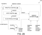
- FIG. 2B depicts a logical block diagram of a power throttle block, or power throttle 170, within an example network switch, according to various aspects of the subject technology.
- Throttle control 280 is able to count the number or rate of incoming ingress packets, and thus cells, for throttling. Further, throttle control 280 may receive ingress scheduler (IS) metadata, for example buffer fill rates. Based on an energy usage estimate from energy estimator 290, throttle control 280 can determine a target clock rate according to configurable throttle policies to meet a target average energy value, which may correspond to a target TDP that is configured for the example network switch. The target clock rate is provided to step control 282, which gradually adjusts the clock rate stepwise towards the target clock rate in adjustment periods after each measurement period.
- IS ingress scheduler
- Step control 282 may send the adjustments to clock regulator 284, which in turn asserts the enable signal (M) at an adjusted rate for a defined number of clock edges (N) at power gating block 230.
- the resulting power gated clock is then fed back to energy estimator 290, which uses defined energy consumption estimates to calculate the estimated energy usage that is provided to throttle control 280.
- the "energy per clock - with packet" may correspond to the estimated energy used when the ingress packets or cells are being processed (and thus enable is asserted)
- the "energy per clock - without packet” may correspond to the estimated energy used when the ingress packets or cells are not being processed (and thus enable is not asserted).
- these values may be calibrated at manufacture time, and in other implementations, these values may be calibrated at run time by actual power consumption measurements, for example by measuring power consumption at various corners of the package die that implements IP 240.
- throttle control 280 can determine a target clock rate to meet a target average energy value, which may correspond to a target TDP that is configured for the example network switch.
- This target average energy value may be averaged for a thermal average period, which may be calibrated to be a relatively long period, such as 100 milliseconds to 10 seconds. This may provide a buffer for burst traffic to be absorbed during each thermal average period to reduce throttling.
- throttle control 280 may assert a reset signal to energy estimator 290, which in turn may perform a reset or initialization of surplus power budgets and other values according to configurable throttle policies for each thermal average period.
- the power throttle 170 may be bypassed by manual override of the target clock rate.
- a host or a controller may manually provide the target clock rate to step control 282, thereby overriding throttle control 280.
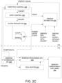
- FIG. 2C depicts a logical block diagram of a power throttle block, or power throttle 170, and a packet processing block 110 within an example network switch, according to various aspects of the subject technology. As shown, FIG. 2C corresponds to a combination of FIG. 2A and FIG. 2B , which is also depicted in simplified form in FIG. 1B .
- FIG. 3A depicts an example graph of power throttling when using a zero budget policy with a constant high load, according to various aspects of the subject technology.
- the example graph may depict a single thermal average period.
- the power gated clock rate or "ThrottleFactor” may be adjustable within a defined range, or a ceiling correspond to "ConfiguredHiClock” and a floor corresponding to "ConfiguredLoClock”.
- throttle control 280 may be configurable with various throttle policies, some which are described in FIGS. 3A-3D .
- the throttle policy corresponds to a "Zero Budget Policy".
- Throttle control 280 may be configured not to adjust the "ThrottleFactor", or target clock rate, beyond the clock rate needed to achieve the target TDP for the thermal average period, or the "Target Energy”, when there is no credit available from the surplus power budget. Since the packet processing workload or "OfferedLoad" is a constant high load, there is no opportunity to fill the surplus power budget, and therefore the clock rate is kept constant without exceeding the "Target Energy” value.
- FIG. 3B depicts an example graph of power throttling when using a zero budget policy with a variable load, according to various aspects of the subject technology.
- the "OfferedLoad” now varies over time, which allows the surplus power budget to be credited when the target clock rate or "Throttle Factor" exceeds the actual adjusted power gated clock rate, which can be measured from the energy usage estimate received from energy estimator 290.
- the step control 282 may gradually adjust the clock rate towards the target clock rate, in which case the power gated clock rate may be less than it could be at that time. The difference between the measured and target clock rate is therefore credited to the surplus power budget.
- the surplus power budget may be expended to raise the "Throttle Factor", as indicated by the upwards triangle portion of the "Throttle Factor”.
- throttling may resume to meet the target energy average for the thermal average period, as indicated by the downwards triangle portion of the "Throttle Factor”.
- the "Throttle Factor” is bounded by the "ConfiguredLoClock” floor and does not throttle any further.
- the conservative zero budget policy helps to conserve power budget to address future high workloads.
- FIG. 3C depicts an example graph of power throttling when using an aggressive ramping policy with a constant high load, according to various aspects of the subject technology.
- energy estimator 290 may set the surplus power budget to an initial non-zero value when a reset signal is received from throttle control 280 to indicate the start of a new thermal average period.
- the "Throttle Factor” may be immediately set to the ceiling, or "ConfiguredHiClock", and remain there until the surplus power budget is exhausted, at which point throttling is incurred and the "Throttle Factor” ramps down to "ConfiguredLoClock" for the remainder of the thermal average period.
- FIG. 3D depicts an example graph of power throttling when using an aggressive ramping policy with a variable load, according to various aspects of the subject technology.
- the aggressive ramping policy since the aggressive ramping policy prioritizes the immediate usage of any surplus power budget, the budget may be quickly exhausted and the "ThrottleFactor" may be forced to throttle towards the end of the thermal average period, as shown.
- the aggressive ramping policy prioritizes burst performance but may quickly exhaust power budget for future workloads. Whether conservative or aggressive ramping is preferred may depend on application latency and jitter requirements.
- a policy corresponds to a buffer fill rate policy. For example, if the buffer fill rate of cell buffer 250 exceeds a upwards threshold, as indicated by the IS metadata, then the "ThrottleFactor" may be set to the maximum possible, or “ConfiguredHiClock”. Similarly, if the buffer fill rate of cell buffer 250 falls below a downwards threshold, then the “ThrottleFactor” may be set to the minimum possible, or "ConfiguredLoClock". In some implementations, multiple threshold levels may be provided so that clock rate targets can be chosen that are distributed between the "ConfiguredHiClock" and "ConfiguredLoClock". This buffer fill rate policy allows the power gated clock rate to quickly ramp according to incoming workload.
- FIG. 4 depicts an example process 400 for providing power throttle for network switches, according to various aspects of the subject technology.
- the various blocks of example process 400 are described herein with reference to FIGS. 1A-3D , and the components and/or processes described herein.
- the one or more of the blocks of process 400 may be implemented, for example, by a computing device, including a processor and other components utilized by the device. In some implementations, one or more of the blocks may be implemented apart from other blocks, and by one or more different processors or devices. Further for explanatory purposes, the blocks of example process 400 are described as occurring in serial, or linearly. However, multiple blocks of example process 400 may occur in parallel. In addition, the blocks of example process 400 need not be performed in the order shown and/or one or more of the blocks of example process 400 need not be performed.
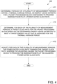
- an energy usage estimate is determined for a packet processing block configured to process ingress packets at a power gated clock rate (411).
- this may correspond to energy estimator 290 determining an energy usage estimate for a plurality of measurement periods within a thermal average period, wherein the energy usage estimate is for IP 240 operating at a power gated clock rate provided by power gating block 230.
- the measurement periods may each correspond to, for example, approximately 1 to 10 percent of the thermal average period.
- the measurement periods may be substantially equal time periods.
- Process 400 may continue with determining, for each of the plurality of measurement periods, a target clock rate for the packet processing block based on the determined energy usage estimates to meet a target energy value that is averaged for the thermal average period (412). Referring to FIG. 2C , this may correspond to throttle control 280 determining, for each of the plurality of measurement periods, a target clock rate for IP 240 based on the energy usage estimates from 411 to meet a target TDP that is averaged for the thermal average period. For example, referring to FIG. 3A-3D , the target TDP that is averaged for the thermal average period may correspond to the depicted "Target Energy" line, wherein FIG. 3A-3D each depict a single thermal average period.
- Process 400 may continue with adjusting, for each of the plurality of measurement periods, the power gated clock rate towards the target clock rate, wherein the adjusting causes the packet processing block to process the ingress packets at the adjusted power gated clock rate (413).
- this may correspond to step control 282 adjusting, for each of the plurality of measurement periods, the power gated clock rate towards the target clock rate from 412.
- this may be done stepwise within a plurality of adjustment periods after each measurement period.
- An adjustment period may correspond to a time length that is 1 to 10 percent of a measurement period.
- the plurality of adjustment periods may correspond to a combined time length of a single measurement period.
- the clock regulator 284 may implement the power gated clock rate by asserting M enable signals out of every N clock edges. As shown in FIG. 2C , this causes the power gated clock to be output to the input of IP 240, which in turn causes IP 240 to process the ingress packets at the adjusted power gated clock rate. The steps of process 400 may be repeated for successive thermal average periods.
- ⁇ process 400 may also be implemented as software processes that are specified as a set of instructions recorded on a computer readable storage medium (also referred to as computer readable medium), and may be executed automatically (e.g., without user intervention).
- a computer readable storage medium also referred to as computer readable medium
- these instructions are executed by one or more processing unit(s) (e.g., one or more processors, cores of processors, or other processing units), they cause the processing unit(s) to perform the actions indicated in the instructions.
- processing unit(s) e.g., one or more processors, cores of processors, or other processing units
- Examples of computer readable media include, but are not limited to, CD-ROMs, flash drives, RAM chips, hard drives, EPROMs, etc.
- the computer readable media does not include carrier waves and electronic signals passing wirelessly or over wired connections.
- the term "software” is meant to include, where appropriate, firmware residing in read-only memory or applications stored in magnetic storage, which can be read into memory for processing by a processor. Also, in some implementations, multiple software aspects of the subject disclosure can be implemented as sub-parts of a larger program while remaining distinct software aspects of the subject disclosure. In some implementations, multiple software aspects can also be implemented as separate programs. Finally, any combination of separate programs that together implement a software aspect described here is within the scope of the subject disclosure. In some implementations, the software programs, when installed to operate on one or more electronic systems, define one or more specific machine implementations that execute and perform the operations of the software programs.
- a computer program (also known as a program, software, software application, script, or code) can be written in any form of programming language, including compiled or interpreted languages, declarative or procedural languages, and it can be deployed in any form, including as a stand-alone program or as a module, component, subroutine, object, or other unit suitable for use in a computing environment.
- a computer program may, but need not, correspond to a file in a file system.
- a program can be stored in a portion of a file that holds other programs or data (e.g., one or more scripts stored in a markup language document), in a single file dedicated to the program in question, or in multiple coordinated files (e.g., files that store one or more modules, sub programs, or portions of code).
- a computer program can be deployed to be executed on one computer or on multiple computers that are located at one site or distributed across multiple sites and interconnected by a communication network.
- FIG. 5 illustrates an electronic system 500 with which one or more implementations of the subject technology may be implemented.
- the electronic system 500 can be, and/or can be a part of, the network switch 104 shown in FIG. 1B .
- the electronic system 500 may include various types of computer readable media and interfaces for various other types of computer readable media.
- the electronic system 500 includes a bus 508, one or more processing unit(s) 512, a system memory 504 (and/or buffer), a ROM 510, a permanent storage device 502, an input device interface 514, an output device interface 506, and one or more network interfaces 516, or subsets and variations thereof.
- the bus 508 collectively represents all system, peripheral, and chipset buses that communicatively connect the numerous internal devices of the electronic system 500.
- the bus 508 communicatively connects the one or more processing unit(s) 512 with the ROM 510, the system memory 504, and the permanent storage device 502. From these various memory units, the one or more processing unit(s) 512 retrieves instructions to execute and data to process in order to execute the processes of the subject disclosure.
- the one or more processing unit(s) 512 can be a single processor or a multi-core processor in different implementations.
- the ROM 510 stores static data and instructions that are needed by the one or more processing unit(s) 512 and other modules of the electronic system 500.
- the permanent storage device 502 may be a read-and-write memory device.
- the permanent storage device 502 may be a non-volatile memory unit that stores instructions and data even when the electronic system 500 is off.
- a mass-storage device (such as a magnetic or optical disk and its corresponding disk drive) may be used as the permanent storage device 502.
- a removable storage device (such as a floppy disk, flash drive, and its corresponding disk drive) may be used as the permanent storage device 502.
- the system memory 504 may be a read-and-write memory device. However, unlike the permanent storage device 502, the system memory 504 may be a volatile read-and-write memory, such as random access memory.
- the system memory 504 may store any of the instructions and data that one or more processing unit(s) 512 may need at runtime.
- the processes of the subject disclosure are stored in the system memory 504, the permanent storage device 502, and/or the ROM 510. From these various memory units, the one or more processing unit(s) 512 retrieves instructions to execute and data to process in order to execute the processes of one or more implementations.
- the bus 508 also connects to the input and output device interfaces 514 and 506.
- the input device interface 514 enables a user to communicate information and select commands to the electronic system 500.
- Input devices that may be used with the input device interface 514 may include, for example, alphanumeric keyboards and pointing devices (also called “cursor control devices").
- the output device interface 506 may enable, for example, the display of images generated by electronic system 500.
- Output devices that may be used with the output device interface 506 may include, for example, printers and display devices, such as a liquid crystal display (LCD), a light emitting diode (LED) display, an organic light emitting diode (OLED) display, a flexible display, a flat panel display, a solid state display, a projector, or any other device for outputting information.
- printers and display devices such as a liquid crystal display (LCD), a light emitting diode (LED) display, an organic light emitting diode (OLED) display, a flexible display, a flat panel display, a solid state display, a projector, or any other device for outputting information.
- One or more implementations may include devices that function as both input and output devices, such as a touchscreen.
- feedback provided to the user can be any form of sensory feedback, such as visual feedback, auditory feedback, or tactile feedback; and input from the user can be received in any form, including acoustic, speech, or tactile input.
- the bus 508 also couples the electronic system 500 to one or more networks and/or to one or more network nodes, through the one or more network interface(s) 516.
- the electronic system 500 can be a part of a network of computers (such as a LAN, a wide area network ("WAN"), or an Intranet, or a network of networks, such as the Internet. Any or all components of the electronic system 500 can be used in conjunction with the subject disclosure.
- Implementations within the scope of the present disclosure can be partially or entirely realized using a tangible computer-readable storage medium (or multiple tangible computer-readable storage media of one or more types) encoding one or more instructions.
- the tangible computer-readable storage medium also can be non-transitory in nature.
- the computer-readable storage medium can be any storage medium that can be read, written, or otherwise accessed by a general purpose or special purpose computing device, including any processing electronics and/or processing circuitry capable of executing instructions.
- the computer-readable medium can include any volatile semiconductor memory, such as RAM, DRAM, SRAM, T-RAM, Z-RAM, and TTRAM.
- the computer-readable medium also can include any non-volatile semiconductor memory, such as ROM, PROM, EPROM, EEPROM, NVRAM, flash, nvSRAM, FeRAM, FeTRAM, MRAM, PRAM, CBRAM, SONOS, RRAM, NRAM, racetrack memory, FJG, and Millipede memory.
- the computer-readable storage medium can include any non-semiconductor memory, such as optical disk storage, magnetic disk storage, magnetic tape, other magnetic storage devices, or any other medium capable of storing one or more instructions.
- the tangible computer-readable storage medium can be directly coupled to a computing device, while in other implementations, the tangible computer-readable storage medium can be indirectly coupled to a computing device, e.g., via one or more wired connections, one or more wireless connections, or any combination thereof.
- Instructions can be directly executable or can be used to develop executable instructions.
- instructions can be realized as executable or non-executable machine code or as instructions in a high-level language that can be compiled to produce executable or non-executable machine code.
- instructions also can be realized as or can include data.
- Computer-executable instructions also can be organized in any format, including routines, subroutines, programs, data structures, objects, modules, applications, applets, functions, etc. As recognized by those of skill in the art, details including, but not limited to, the number, structure, sequence, and organization of instructions can vary significantly without varying the underlying logic, function, processing, and output.
- any specific order or hierarchy of blocks in the processes disclosed is an illustration of example approaches. Based upon design preferences, it is understood that the specific order or hierarchy of blocks in the processes may be rearranged, or that all illustrated blocks be performed. Any of the blocks may be performed simultaneously. In one or more implementations, multitasking and parallel processing may be advantageous. Moreover, the separation of various system components in the embodiments described above should not be understood as requiring such separation in all embodiments, and it should be understood that the described program components and systems can generally be integrated together in a single software product or packaged into multiple software products.
- base station As used in this specification and any claims of this application, the terms “base station”, “receiver”, “computer”, “server”, “processor”, and “memory” all refer to electronic or other technological devices. These terms exclude people or groups of people.
- display or “displaying” means displaying on an electronic device.
- the phrase "at least one of” preceding a series of items, with the term “and” or “or” to separate any of the items, modifies the list as a whole, rather than each member of the list (i.e., each item).
- the phrase "at least one of” does not require selection of at least one of each item listed; rather, the phrase allows a meaning that includes at least one of any one of the items, and/or at least one of any combination of the items, and/or at least one of each of the items.
- phrases “at least one of A, B, and C” or “at least one of A, B, or C” each refer to only A, only B, or only C; any combination of A, B, and C; and/or at least one of each of A, B, and C.
- a processor configured to monitor and control an operation or a component may also mean the processor being programmed to monitor and control the operation or the processor being operable to monitor and control the operation.
- a processor configured to execute code can be construed as a processor programmed to execute code or operable to execute code.
- phrases such as an aspect, the aspect, another aspect, some aspects, one or more aspects, an implementation, the implementation, another implementation, some implementations, one or more implementations, an embodiment, the embodiment, another embodiment, some embodiments, one or more embodiments, a configuration, the configuration, another configuration, some configurations, one or more configurations, the subject technology, the disclosure, the present disclosure, other variations thereof and alike are for convenience and do not imply that a disclosure relating to such phrase(s) is essential to the subject technology or that such disclosure applies to all configurations of the subject technology.
- a disclosure relating to such phrase(s) may apply to all configurations, or one or more configurations.
- a disclosure relating to such phrase(s) may provide one or more examples.
- a phrase such as an aspect or some aspects may refer to one or more aspects and vice versa, and this applies similarly to other foregoing phrases.
Landscapes
- Engineering & Computer Science (AREA)
- Theoretical Computer Science (AREA)
- Physics & Mathematics (AREA)
- General Engineering & Computer Science (AREA)
- General Physics & Mathematics (AREA)
- Computer Networks & Wireless Communication (AREA)
- Signal Processing (AREA)
- Power Sources (AREA)
- Data Exchanges In Wide-Area Networks (AREA)
Claims (11)
- System, konfiguriert zumBestimmen (411) einer Energieverbrauchsabschätzung für einen Paketverarbeitungsblock (110) für jede einer Vielzahl von Messperioden innerhalb einer thermischen Durchschnittsperiode,Bestimmen (412) einer Zieltaktrate für einen Paketverarbeitungsblock (110) für jede der Vielzahl von Messperioden auf der Grundlage der bestimmten Energieverbrauchsabschätzung, um einen Zielenergiewert zu erfüllen, der für die thermische Durchschnittsperiode gemittelt ist; undEinstellen (413) einer Taktrate in Richtung der Zieltaktrate für jede der Vielzahl von Messperioden, um zu veranlassen, dass der Paketverarbeitungsblock (110) Eingangspakete mit der eingestellten Taktrate verarbeitet;dadurch gekennzeichnet, dassdas System konfiguriert ist zum Bestimmen der Zieltaktrate auf der Grundlage, ob eine Pufferfüllrate für die Eingangspakete eine Schwellenfüllrate überschreitet.
- System nach Anspruch 1, wobei das System konfiguriert ist zum Einstellen der Taktrate unter Verwendung einer Vielzahl von Einstellperioden nach der Messperiode.
- System nach einem vorhergehenden Anspruch, wobei die Zieltaktrate für den Paketverarbeitungsblock (110) auf der Grundlage eines Zielenergiewerts bestimmt wird.
- System nach einem vorhergehenden Anspruch, wobei die thermische Durchschnittsperiode etwa 100 Millisekunden bis 10 Sekunden beträgt.
- System nach einem vorhergehenden Anspruch, wobei die Zieltaktrate durch einen vorgegebenen Bereich begrenzt ist.
- System nach einem vorhergehenden Anspruch, wobei das System konfiguriert ist zum Bestimmen der Zieltaktrate auf der Grundlage eines Überschussenergiebudgets, das gutgeschrieben wird, während die Zieltaktrate die eingestellte Taktrate überschreitet.
- System nach Anspruch 6, wobei das Überschussenergiebudget zu Beginn der thermischen Durchschnittsperiode entweder auf null oder auf einen anfänglichen Budgetwert gesetzt wird.
- System nach einem vorhergehenden Anspruch, wobei mehrere Schwellenwerte für die Schwellenfüllrate vorgesehen sind.
- Verfahren, umfassend:Bestimmen (411) einer Energieverbrauchsschätzung für einen Paketverarbeitungsblock (110) für jede einer Vielzahl von Messperioden innerhalb einer thermischen Durchschnittsperiode,Bestimmen (412), für jede der Vielzahl von Messperioden, einer Zieltaktrate für einen Paketverarbeitungsblock (110), um einen Zielenergiewert zu erfüllen, der für die thermische Durchschnittsperiode gemittelt ist; undEinstellen (413) einer Taktrate für jede der Vielzahl von Messperioden in Richtung der Zieltaktrate, um den Paketverarbeitungsblock (110) zu veranlassen, Eingangspakete mit der eingestellten Taktrate zu verarbeiten;dadurch gekennzeichnet, dassdie Zieltaktrate auf der Grundlage bestimmt wird, ob eine Pufferfüllrate für die Eingangspakete eine Schwellenfüllrate überschreitet.
- Verfahren nach Anspruch 9, wobei die Zieltaktrate auf der Grundlage einer bestimmten Energieverbrauchsschätzung bestimmt wird.
- Verfahren nach Anspruch 9 oder 10, wobei die Zieltaktrate für den Paketverarbeitungsblock (110) auf der Grundlage eines Zielenergiewerts bestimmt wird.
Priority Applications (1)
| Application Number | Priority Date | Filing Date | Title |
|---|---|---|---|
| EP25174685.5A EP4592798A3 (de) | 2020-07-31 | 2021-07-27 | Leistungsdrossel für netzwerkschalter |
Applications Claiming Priority (2)
| Application Number | Priority Date | Filing Date | Title |
|---|---|---|---|
| US16/945,562 US11368412B2 (en) | 2020-07-31 | 2020-07-31 | Power throttle for network switches |
| EP21187888.9A EP3945400B1 (de) | 2020-07-31 | 2021-07-27 | Leistungsdrossel für netzschalter |
Related Parent Applications (2)
| Application Number | Title | Priority Date | Filing Date |
|---|---|---|---|
| EP21187888.9A Division-Into EP3945400B1 (de) | 2020-07-31 | 2021-07-27 | Leistungsdrossel für netzschalter |
| EP21187888.9A Division EP3945400B1 (de) | 2020-07-31 | 2021-07-27 | Leistungsdrossel für netzschalter |
Related Child Applications (2)
| Application Number | Title | Priority Date | Filing Date |
|---|---|---|---|
| EP25174685.5A Division EP4592798A3 (de) | 2020-07-31 | 2021-07-27 | Leistungsdrossel für netzwerkschalter |
| EP25174685.5A Division-Into EP4592798A3 (de) | 2020-07-31 | 2021-07-27 | Leistungsdrossel für netzwerkschalter |
Publications (4)
| Publication Number | Publication Date |
|---|---|
| EP4290336A2 EP4290336A2 (de) | 2023-12-13 |
| EP4290336A3 EP4290336A3 (de) | 2024-02-21 |
| EP4290336C0 EP4290336C0 (de) | 2025-06-11 |
| EP4290336B1 true EP4290336B1 (de) | 2025-06-11 |
Family
ID=77367219
Family Applications (3)
| Application Number | Title | Priority Date | Filing Date |
|---|---|---|---|
| EP23198432.9A Active EP4290336B1 (de) | 2020-07-31 | 2021-07-27 | Leistungsdrossel für netzschalter |
| EP25174685.5A Pending EP4592798A3 (de) | 2020-07-31 | 2021-07-27 | Leistungsdrossel für netzwerkschalter |
| EP21187888.9A Active EP3945400B1 (de) | 2020-07-31 | 2021-07-27 | Leistungsdrossel für netzschalter |
Family Applications After (2)
| Application Number | Title | Priority Date | Filing Date |
|---|---|---|---|
| EP25174685.5A Pending EP4592798A3 (de) | 2020-07-31 | 2021-07-27 | Leistungsdrossel für netzwerkschalter |
| EP21187888.9A Active EP3945400B1 (de) | 2020-07-31 | 2021-07-27 | Leistungsdrossel für netzschalter |
Country Status (3)
| Country | Link |
|---|---|
| US (2) | US11368412B2 (de) |
| EP (3) | EP4290336B1 (de) |
| CN (1) | CN114095287B (de) |
Families Citing this family (18)
| Publication number | Priority date | Publication date | Assignee | Title |
|---|---|---|---|---|
| US11411925B2 (en) | 2019-12-31 | 2022-08-09 | Oracle International Corporation | Methods, systems, and computer readable media for implementing indirect general packet radio service (GPRS) tunneling protocol (GTP) firewall filtering using diameter agent and signal transfer point (STP) |
| US11553342B2 (en) | 2020-07-14 | 2023-01-10 | Oracle International Corporation | Methods, systems, and computer readable media for mitigating 5G roaming security attacks using security edge protection proxy (SEPP) |
| US11368412B2 (en) * | 2020-07-31 | 2022-06-21 | Avago Technologies International Sales Pte. Limited | Power throttle for network switches |
| US11751056B2 (en) | 2020-08-31 | 2023-09-05 | Oracle International Corporation | Methods, systems, and computer readable media for 5G user equipment (UE) historical mobility tracking and security screening using mobility patterns |
| US11832172B2 (en) | 2020-09-25 | 2023-11-28 | Oracle International Corporation | Methods, systems, and computer readable media for mitigating spoofing attacks on security edge protection proxy (SEPP) inter-public land mobile network (inter-PLMN) forwarding interface |
| US11825310B2 (en) | 2020-09-25 | 2023-11-21 | Oracle International Corporation | Methods, systems, and computer readable media for mitigating 5G roaming spoofing attacks |
| US11622255B2 (en) | 2020-10-21 | 2023-04-04 | Oracle International Corporation | Methods, systems, and computer readable media for validating a session management function (SMF) registration request |
| US11528251B2 (en) * | 2020-11-06 | 2022-12-13 | Oracle International Corporation | Methods, systems, and computer readable media for ingress message rate limiting |
| US11770694B2 (en) | 2020-11-16 | 2023-09-26 | Oracle International Corporation | Methods, systems, and computer readable media for validating location update messages |
| US11818570B2 (en) | 2020-12-15 | 2023-11-14 | Oracle International Corporation | Methods, systems, and computer readable media for message validation in fifth generation (5G) communications networks |
| US11812271B2 (en) | 2020-12-17 | 2023-11-07 | Oracle International Corporation | Methods, systems, and computer readable media for mitigating 5G roaming attacks for internet of things (IoT) devices based on expected user equipment (UE) behavior patterns |
| US11700510B2 (en) | 2021-02-12 | 2023-07-11 | Oracle International Corporation | Methods, systems, and computer readable media for short message delivery status report validation |
| US11516671B2 (en) | 2021-02-25 | 2022-11-29 | Oracle International Corporation | Methods, systems, and computer readable media for mitigating location tracking and denial of service (DoS) attacks that utilize access and mobility management function (AMF) location service |
| US11689912B2 (en) | 2021-05-12 | 2023-06-27 | Oracle International Corporation | Methods, systems, and computer readable media for conducting a velocity check for outbound subscribers roaming to neighboring countries |
| US12015923B2 (en) | 2021-12-21 | 2024-06-18 | Oracle International Corporation | Methods, systems, and computer readable media for mitigating effects of access token misuse |
| US20240094798A1 (en) * | 2022-05-16 | 2024-03-21 | Marvell Asia Pte Ltd | Managing power in an electronic device |
| US12335146B2 (en) | 2023-06-14 | 2025-06-17 | International Business Machines Corporation | Dynamic, condition-based network device continuity optimization |
| US20250251770A1 (en) * | 2024-02-05 | 2025-08-07 | Mellanox Technologies, Ltd. | Power-aware control plane |
Family Cites Families (11)
| Publication number | Priority date | Publication date | Assignee | Title |
|---|---|---|---|---|
| US7562234B2 (en) * | 2005-08-25 | 2009-07-14 | Apple Inc. | Methods and apparatuses for dynamic power control |
| US8782456B2 (en) * | 2010-06-01 | 2014-07-15 | Intel Corporation | Dynamic and idle power reduction sequence using recombinant clock and power gating |
| US8984216B2 (en) * | 2010-09-09 | 2015-03-17 | Fusion-Io, Llc | Apparatus, system, and method for managing lifetime of a storage device |
| US8612781B2 (en) * | 2010-12-14 | 2013-12-17 | Advanced Micro Devices, Inc. | Method and apparatus for application of power density multipliers optimally in a multicore system |
| US9141166B2 (en) * | 2011-12-13 | 2015-09-22 | Intel Corporation | Method, apparatus, and system for energy efficiency and energy conservation including dynamic control of energy consumption in power domains |
| US9250665B2 (en) * | 2012-06-07 | 2016-02-02 | Apple Inc. | GPU with dynamic performance adjustment |
| US9270396B2 (en) * | 2013-04-11 | 2016-02-23 | Tellabs Operations, Inc. | Method and apparatus for providing timing analysis for packet streams over packet carriers |
| US20150378407A1 (en) * | 2015-09-04 | 2015-12-31 | Mediatek Inc. | Loading-Based Dynamic Voltage And Frequency Scaling |
| KR20180107351A (ko) * | 2017-03-16 | 2018-10-02 | 에스케이하이닉스 주식회사 | 상변화메모리의 전력소모량 연산장치 및 이를 포함하는 상변화메모리 시스템과, 상변화메모리의 전력소모량 연산방법 |
| CN107171441B (zh) * | 2017-07-14 | 2020-02-21 | 国网山东省电力公司淄博供电公司 | 一种具有时钟同步和位置定位功能的电力信息网 |
| US11368412B2 (en) * | 2020-07-31 | 2022-06-21 | Avago Technologies International Sales Pte. Limited | Power throttle for network switches |
-
2020
- 2020-07-31 US US16/945,562 patent/US11368412B2/en active Active
-
2021
- 2021-07-02 CN CN202110747970.8A patent/CN114095287B/zh active Active
- 2021-07-27 EP EP23198432.9A patent/EP4290336B1/de active Active
- 2021-07-27 EP EP25174685.5A patent/EP4592798A3/de active Pending
- 2021-07-27 EP EP21187888.9A patent/EP3945400B1/de active Active
-
2022
- 2022-06-21 US US17/845,854 patent/US11909670B2/en active Active
Also Published As
| Publication number | Publication date |
|---|---|
| US11368412B2 (en) | 2022-06-21 |
| EP4592798A3 (de) | 2025-08-27 |
| CN114095287A (zh) | 2022-02-25 |
| EP3945400B1 (de) | 2023-10-25 |
| EP4290336A2 (de) | 2023-12-13 |
| US11909670B2 (en) | 2024-02-20 |
| US20220038394A1 (en) | 2022-02-03 |
| US20220321504A1 (en) | 2022-10-06 |
| CN114095287B (zh) | 2024-04-12 |
| EP4290336A3 (de) | 2024-02-21 |
| EP4592798A2 (de) | 2025-07-30 |
| EP4290336C0 (de) | 2025-06-11 |
| EP3945400A1 (de) | 2022-02-02 |
Similar Documents
| Publication | Publication Date | Title |
|---|---|---|
| EP4290336B1 (de) | Leistungsdrossel für netzschalter | |
| US11147186B2 (en) | Predictive fan control using workload profiles | |
| US8261112B2 (en) | Optimizing power consumption by tracking how program runtime performance metrics respond to changes in operating frequency | |
| US10444819B2 (en) | Techniques to control computational resources for an electronic device | |
| US8150561B2 (en) | Heat dissipation system for computers | |
| CN107678855B (zh) | 处理器动态调节方法、装置及处理器芯片 | |
| US9261949B2 (en) | Method for adaptive performance optimization of the soc | |
| US9671839B2 (en) | Information handling system dynamic acoustical management | |
| US20170147055A1 (en) | Systems and methods for providing local hardware limit management and enforcement | |
| US20160162297A1 (en) | Thermal Profile Based on Temperature Information for Computing Device Location | |
| US10761592B2 (en) | Power subsystem-monitoring-based graphics processing system | |
| US20190286214A1 (en) | Metering gpu workload with real time feedback from a power sensor or block activity to maintain below predetermined power budget | |
| CN110308782A (zh) | 功耗预测、控制方法、设备及计算机可读存储介质 | |
| CN103488532A (zh) | 一种调整处理器频率的方法和设备 | |
| KR101707096B1 (ko) | 일반 호스트 기반 제어기 레이턴시 방법 및 장치 | |
| EP2954385A1 (de) | System und verfahren zur steuerung der leistung einer zentralen prozessoreinheit mit garantierten transienten fristen | |
| US8135966B2 (en) | Method and device for power management | |
| US10275007B2 (en) | Performance management for a multiple-CPU platform | |
| US9117511B2 (en) | Control circuits for asynchronous circuits | |
| CN120469552A (zh) | 基于动态温控的ssd固态硬盘散热优化方法及系统 | |
| KR102067680B1 (ko) | Cpu 전력 절감 방법 및 장치 | |
| Ahn | Real-time task scheduling under thermal constraints | |
| TWI475371B (zh) | 電子裝置與其電源管理方法 | |
| CN116974359A (zh) | 处理器运行控制方法、装置、电子设备及可读存储介质 |
Legal Events
| Date | Code | Title | Description |
|---|---|---|---|
| PUAI | Public reference made under article 153(3) epc to a published international application that has entered the european phase |
Free format text: ORIGINAL CODE: 0009012 |
|
| STAA | Information on the status of an ep patent application or granted ep patent |
Free format text: STATUS: THE APPLICATION HAS BEEN PUBLISHED |
|
| AC | Divisional application: reference to earlier application |
Ref document number: 3945400 Country of ref document: EP Kind code of ref document: P |
|
| AK | Designated contracting states |
Kind code of ref document: A2 Designated state(s): AL AT BE BG CH CY CZ DE DK EE ES FI FR GB GR HR HU IE IS IT LI LT LU LV MC MK MT NL NO PL PT RO RS SE SI SK SM TR |
|
| REG | Reference to a national code |
Ref country code: DE Ref legal event code: R079 Free format text: PREVIOUS MAIN CLASS: G06F0001323700 Ipc: G06F0001320600 Ref country code: DE Ref legal event code: R079 Ref document number: 602021032304 Country of ref document: DE Free format text: PREVIOUS MAIN CLASS: G06F0001323700 Ipc: G06F0001320600 |
|
| PUAL | Search report despatched |
Free format text: ORIGINAL CODE: 0009013 |
|
| AK | Designated contracting states |
Kind code of ref document: A3 Designated state(s): AL AT BE BG CH CY CZ DE DK EE ES FI FR GB GR HR HU IE IS IT LI LT LU LV MC MK MT NL NO PL PT RO RS SE SI SK SM TR |
|
| RIC1 | Information provided on ipc code assigned before grant |
Ipc: G06F 1/3237 20190101ALI20240112BHEP Ipc: G06F 1/3234 20190101ALI20240112BHEP Ipc: G06F 1/324 20190101ALI20240112BHEP Ipc: G06F 1/3206 20190101AFI20240112BHEP |
|
| STAA | Information on the status of an ep patent application or granted ep patent |
Free format text: STATUS: REQUEST FOR EXAMINATION WAS MADE |
|
| 17P | Request for examination filed |
Effective date: 20240821 |
|
| RBV | Designated contracting states (corrected) |
Designated state(s): AL AT BE BG CH CY CZ DE DK EE ES FI FR GB GR HR HU IE IS IT LI LT LU LV MC MK MT NL NO PL PT RO RS SE SI SK SM TR |
|
| GRAP | Despatch of communication of intention to grant a patent |
Free format text: ORIGINAL CODE: EPIDOSNIGR1 |
|
| STAA | Information on the status of an ep patent application or granted ep patent |
Free format text: STATUS: GRANT OF PATENT IS INTENDED |
|
| RIC1 | Information provided on ipc code assigned before grant |
Ipc: G06F 1/3237 20190101ALI20250117BHEP Ipc: G06F 1/3234 20190101ALI20250117BHEP Ipc: G06F 1/324 20190101ALI20250117BHEP Ipc: G06F 1/3206 20190101AFI20250117BHEP |
|
| INTG | Intention to grant announced |
Effective date: 20250130 |
|
| GRAS | Grant fee paid |
Free format text: ORIGINAL CODE: EPIDOSNIGR3 |
|
| GRAA | (expected) grant |
Free format text: ORIGINAL CODE: 0009210 |
|
| STAA | Information on the status of an ep patent application or granted ep patent |
Free format text: STATUS: THE PATENT HAS BEEN GRANTED |
|
| AC | Divisional application: reference to earlier application |
Ref document number: 3945400 Country of ref document: EP Kind code of ref document: P |
|
| AK | Designated contracting states |
Kind code of ref document: B1 Designated state(s): AL AT BE BG CH CY CZ DE DK EE ES FI FR GB GR HR HU IE IS IT LI LT LU LV MC MK MT NL NO PL PT RO RS SE SI SK SM TR |
|
| REG | Reference to a national code |
Ref country code: GB Ref legal event code: FG4D |
|
| REG | Reference to a national code |
Ref country code: CH Ref legal event code: EP |
|
| REG | Reference to a national code |
Ref country code: DE Ref legal event code: R096 Ref document number: 602021032304 Country of ref document: DE |
|
| REG | Reference to a national code |
Ref country code: IE Ref legal event code: FG4D |
|
| U01 | Request for unitary effect filed |
Effective date: 20250611 |
|
| U07 | Unitary effect registered |
Designated state(s): AT BE BG DE DK EE FI FR IT LT LU LV MT NL PT RO SE SI Effective date: 20250620 |
|
| U20 | Renewal fee for the european patent with unitary effect paid |
Year of fee payment: 5 Effective date: 20250709 |
|
| PG25 | Lapsed in a contracting state [announced via postgrant information from national office to epo] |
Ref country code: ES Free format text: LAPSE BECAUSE OF FAILURE TO SUBMIT A TRANSLATION OF THE DESCRIPTION OR TO PAY THE FEE WITHIN THE PRESCRIBED TIME-LIMIT Effective date: 20250611 |
|
| PG25 | Lapsed in a contracting state [announced via postgrant information from national office to epo] |
Ref country code: GR Free format text: LAPSE BECAUSE OF FAILURE TO SUBMIT A TRANSLATION OF THE DESCRIPTION OR TO PAY THE FEE WITHIN THE PRESCRIBED TIME-LIMIT Effective date: 20250912 Ref country code: NO Free format text: LAPSE BECAUSE OF FAILURE TO SUBMIT A TRANSLATION OF THE DESCRIPTION OR TO PAY THE FEE WITHIN THE PRESCRIBED TIME-LIMIT Effective date: 20250911 |
|
| PG25 | Lapsed in a contracting state [announced via postgrant information from national office to epo] |
Ref country code: HR Free format text: LAPSE BECAUSE OF FAILURE TO SUBMIT A TRANSLATION OF THE DESCRIPTION OR TO PAY THE FEE WITHIN THE PRESCRIBED TIME-LIMIT Effective date: 20250611 |
|
| PG25 | Lapsed in a contracting state [announced via postgrant information from national office to epo] |
Ref country code: RS Free format text: LAPSE BECAUSE OF FAILURE TO SUBMIT A TRANSLATION OF THE DESCRIPTION OR TO PAY THE FEE WITHIN THE PRESCRIBED TIME-LIMIT Effective date: 20250911 |
|
| PG25 | Lapsed in a contracting state [announced via postgrant information from national office to epo] |
Ref country code: IS Free format text: LAPSE BECAUSE OF FAILURE TO SUBMIT A TRANSLATION OF THE DESCRIPTION OR TO PAY THE FEE WITHIN THE PRESCRIBED TIME-LIMIT Effective date: 20251011 |
|
| PG25 | Lapsed in a contracting state [announced via postgrant information from national office to epo] |
Ref country code: SM Free format text: LAPSE BECAUSE OF FAILURE TO SUBMIT A TRANSLATION OF THE DESCRIPTION OR TO PAY THE FEE WITHIN THE PRESCRIBED TIME-LIMIT Effective date: 20250611 |
|
| PG25 | Lapsed in a contracting state [announced via postgrant information from national office to epo] |
Ref country code: CZ Free format text: LAPSE BECAUSE OF FAILURE TO SUBMIT A TRANSLATION OF THE DESCRIPTION OR TO PAY THE FEE WITHIN THE PRESCRIBED TIME-LIMIT Effective date: 20250611 |
|
| PG25 | Lapsed in a contracting state [announced via postgrant information from national office to epo] |
Ref country code: PL Free format text: LAPSE BECAUSE OF FAILURE TO SUBMIT A TRANSLATION OF THE DESCRIPTION OR TO PAY THE FEE WITHIN THE PRESCRIBED TIME-LIMIT Effective date: 20250611 |
|
| PG25 | Lapsed in a contracting state [announced via postgrant information from national office to epo] |
Ref country code: SK Free format text: LAPSE BECAUSE OF FAILURE TO SUBMIT A TRANSLATION OF THE DESCRIPTION OR TO PAY THE FEE WITHIN THE PRESCRIBED TIME-LIMIT Effective date: 20250611 |
|
| REG | Reference to a national code |
Ref country code: CH Ref legal event code: H13 Free format text: ST27 STATUS EVENT CODE: U-0-0-H10-H13 (AS PROVIDED BY THE NATIONAL OFFICE) Effective date: 20260224 |
|
| PG25 | Lapsed in a contracting state [announced via postgrant information from national office to epo] |
Ref country code: MC Free format text: LAPSE BECAUSE OF FAILURE TO SUBMIT A TRANSLATION OF THE DESCRIPTION OR TO PAY THE FEE WITHIN THE PRESCRIBED TIME-LIMIT Effective date: 20250611 |
|
| PLBE | No opposition filed within time limit |
Free format text: ORIGINAL CODE: 0009261 |
|
| STAA | Information on the status of an ep patent application or granted ep patent |
Free format text: STATUS: NO OPPOSITION FILED WITHIN TIME LIMIT |
|
| PG25 | Lapsed in a contracting state [announced via postgrant information from national office to epo] |
Ref country code: CH Free format text: LAPSE BECAUSE OF NON-PAYMENT OF DUE FEES Effective date: 20250731 |
|
| REG | Reference to a national code |
Ref country code: CH Ref legal event code: L10 Free format text: ST27 STATUS EVENT CODE: U-0-0-L10-L00 (AS PROVIDED BY THE NATIONAL OFFICE) Effective date: 20260423 |