EP4290331A1 - Electronic device comprising flexible display - Google Patents
Electronic device comprising flexible display Download PDFInfo
- Publication number
- EP4290331A1 EP4290331A1 EP22833416.5A EP22833416A EP4290331A1 EP 4290331 A1 EP4290331 A1 EP 4290331A1 EP 22833416 A EP22833416 A EP 22833416A EP 4290331 A1 EP4290331 A1 EP 4290331A1
- Authority
- EP
- European Patent Office
- Prior art keywords
- patterns
- electronic device
- housing
- region
- layer
- Prior art date
- Legal status (The legal status is an assumption and is not a legal conclusion. Google has not performed a legal analysis and makes no representation as to the accuracy of the status listed.)
- Pending
Links
- 239000011521 glass Substances 0.000 claims abstract description 144
- 238000005530 etching Methods 0.000 claims abstract description 69
- 239000010410 layer Substances 0.000 claims description 270
- 239000000463 material Substances 0.000 claims description 25
- 239000011241 protective layer Substances 0.000 claims description 10
- 239000000945 filler Substances 0.000 claims description 5
- 239000002861 polymer material Substances 0.000 claims description 4
- 230000007246 mechanism Effects 0.000 description 31
- 238000005452 bending Methods 0.000 description 27
- 229910052751 metal Inorganic materials 0.000 description 22
- 239000002184 metal Substances 0.000 description 21
- 229920000642 polymer Polymers 0.000 description 16
- 238000010586 diagram Methods 0.000 description 15
- 229920002120 photoresistant polymer Polymers 0.000 description 11
- 238000000034 method Methods 0.000 description 8
- 230000036961 partial effect Effects 0.000 description 8
- 230000008569 process Effects 0.000 description 8
- 230000003014 reinforcing effect Effects 0.000 description 7
- 239000010935 stainless steel Substances 0.000 description 6
- 229910001220 stainless steel Inorganic materials 0.000 description 6
- 239000000853 adhesive Substances 0.000 description 5
- 238000004891 communication Methods 0.000 description 5
- 239000000758 substrate Substances 0.000 description 5
- 238000004519 manufacturing process Methods 0.000 description 4
- 230000000873 masking effect Effects 0.000 description 4
- 101001045744 Sus scrofa Hepatocyte nuclear factor 1-beta Proteins 0.000 description 3
- 230000001070 adhesive effect Effects 0.000 description 3
- 229910052782 aluminium Inorganic materials 0.000 description 3
- 230000008859 change Effects 0.000 description 3
- 238000002834 transmittance Methods 0.000 description 3
- 229920002430 Fibre-reinforced plastic Polymers 0.000 description 2
- FYYHWMGAXLPEAU-UHFFFAOYSA-N Magnesium Chemical compound [Mg] FYYHWMGAXLPEAU-UHFFFAOYSA-N 0.000 description 2
- 239000004820 Pressure-sensitive adhesive Substances 0.000 description 2
- 230000001133 acceleration Effects 0.000 description 2
- XAGFODPZIPBFFR-UHFFFAOYSA-N aluminium Chemical compound [Al] XAGFODPZIPBFFR-UHFFFAOYSA-N 0.000 description 2
- 230000005540 biological transmission Effects 0.000 description 2
- 239000004918 carbon fiber reinforced polymer Substances 0.000 description 2
- 239000000919 ceramic Substances 0.000 description 2
- 238000005034 decoration Methods 0.000 description 2
- 230000000694 effects Effects 0.000 description 2
- 230000007613 environmental effect Effects 0.000 description 2
- 239000011151 fibre-reinforced plastic Substances 0.000 description 2
- 239000011152 fibreglass Substances 0.000 description 2
- 229910052749 magnesium Inorganic materials 0.000 description 2
- 239000011777 magnesium Substances 0.000 description 2
- 238000003825 pressing Methods 0.000 description 2
- 230000002829 reductive effect Effects 0.000 description 2
- 239000011347 resin Substances 0.000 description 2
- 229920005989 resin Polymers 0.000 description 2
- 239000000126 substance Substances 0.000 description 2
- 239000010409 thin film Substances 0.000 description 2
- 229910052724 xenon Inorganic materials 0.000 description 2
- FHNFHKCVQCLJFQ-UHFFFAOYSA-N xenon atom Chemical compound [Xe] FHNFHKCVQCLJFQ-UHFFFAOYSA-N 0.000 description 2
- OKTJSMMVPCPJKN-UHFFFAOYSA-N Carbon Chemical compound [C] OKTJSMMVPCPJKN-UHFFFAOYSA-N 0.000 description 1
- JOYRKODLDBILNP-UHFFFAOYSA-N Ethyl urethane Chemical compound CCOC(N)=O JOYRKODLDBILNP-UHFFFAOYSA-N 0.000 description 1
- 239000004642 Polyimide Substances 0.000 description 1
- 239000004823 Reactive adhesive Substances 0.000 description 1
- 229910000831 Steel Inorganic materials 0.000 description 1
- NIXOWILDQLNWCW-UHFFFAOYSA-N acrylic acid group Chemical group C(C=C)(=O)O NIXOWILDQLNWCW-UHFFFAOYSA-N 0.000 description 1
- 239000000956 alloy Substances 0.000 description 1
- 230000003139 buffering effect Effects 0.000 description 1
- 229910052802 copper Inorganic materials 0.000 description 1
- 230000007423 decrease Effects 0.000 description 1
- 238000001514 detection method Methods 0.000 description 1
- 238000004090 dissolution Methods 0.000 description 1
- 230000005674 electromagnetic induction Effects 0.000 description 1
- 239000010408 film Substances 0.000 description 1
- 229910002804 graphite Inorganic materials 0.000 description 1
- 239000010439 graphite Substances 0.000 description 1
- 230000017525 heat dissipation Effects 0.000 description 1
- 230000000670 limiting effect Effects 0.000 description 1
- 239000007788 liquid Substances 0.000 description 1
- 239000007769 metal material Substances 0.000 description 1
- 229910052755 nonmetal Inorganic materials 0.000 description 1
- 230000003287 optical effect Effects 0.000 description 1
- 229920001721 polyimide Polymers 0.000 description 1
- 229920001296 polysiloxane Polymers 0.000 description 1
- 238000012805 post-processing Methods 0.000 description 1
- 238000012545 processing Methods 0.000 description 1
- 230000002787 reinforcement Effects 0.000 description 1
- 230000004044 response Effects 0.000 description 1
- 238000005096 rolling process Methods 0.000 description 1
- 239000007787 solid Substances 0.000 description 1
- 238000007711 solidification Methods 0.000 description 1
- 230000008023 solidification Effects 0.000 description 1
- 230000005236 sound signal Effects 0.000 description 1
- 239000010959 steel Substances 0.000 description 1
- 239000012780 transparent material Substances 0.000 description 1
- 238000004078 waterproofing Methods 0.000 description 1
Images


Classifications
-
- H—ELECTRICITY
- H04—ELECTRIC COMMUNICATION TECHNIQUE
- H04M—TELEPHONIC COMMUNICATION
- H04M1/00—Substation equipment, e.g. for use by subscribers
- H04M1/02—Constructional features of telephone sets
- H04M1/0202—Portable telephone sets, e.g. cordless phones, mobile phones or bar type handsets
- H04M1/026—Details of the structure or mounting of specific components
- H04M1/0266—Details of the structure or mounting of specific components for a display module assembly
- H04M1/0268—Details of the structure or mounting of specific components for a display module assembly including a flexible display panel
-
- G—PHYSICS
- G06—COMPUTING; CALCULATING OR COUNTING
- G06F—ELECTRIC DIGITAL DATA PROCESSING
- G06F1/00—Details not covered by groups G06F3/00 - G06F13/00 and G06F21/00
- G06F1/16—Constructional details or arrangements
- G06F1/1613—Constructional details or arrangements for portable computers
- G06F1/1633—Constructional details or arrangements of portable computers not specific to the type of enclosures covered by groups G06F1/1615 - G06F1/1626
- G06F1/1656—Details related to functional adaptations of the enclosure, e.g. to provide protection against EMI, shock, water, or to host detachable peripherals like a mouse or removable expansions units like PCMCIA cards, or to provide access to internal components for maintenance or to removable storage supports like CDs or DVDs, or to mechanically mount accessories
-
- G—PHYSICS
- G06—COMPUTING; CALCULATING OR COUNTING
- G06F—ELECTRIC DIGITAL DATA PROCESSING
- G06F1/00—Details not covered by groups G06F3/00 - G06F13/00 and G06F21/00
- G06F1/16—Constructional details or arrangements
- G06F1/1613—Constructional details or arrangements for portable computers
- G06F1/1633—Constructional details or arrangements of portable computers not specific to the type of enclosures covered by groups G06F1/1615 - G06F1/1626
- G06F1/1637—Details related to the display arrangement, including those related to the mounting of the display in the housing
- G06F1/1652—Details related to the display arrangement, including those related to the mounting of the display in the housing the display being flexible, e.g. mimicking a sheet of paper, or rollable
-
- C—CHEMISTRY; METALLURGY
- C03—GLASS; MINERAL OR SLAG WOOL
- C03C—CHEMICAL COMPOSITION OF GLASSES, GLAZES OR VITREOUS ENAMELS; SURFACE TREATMENT OF GLASS; SURFACE TREATMENT OF FIBRES OR FILAMENTS MADE FROM GLASS, MINERALS OR SLAGS; JOINING GLASS TO GLASS OR OTHER MATERIALS
- C03C15/00—Surface treatment of glass, not in the form of fibres or filaments, by etching
-
- G—PHYSICS
- G06—COMPUTING; CALCULATING OR COUNTING
- G06F—ELECTRIC DIGITAL DATA PROCESSING
- G06F1/00—Details not covered by groups G06F3/00 - G06F13/00 and G06F21/00
- G06F1/16—Constructional details or arrangements
-
- G—PHYSICS
- G06—COMPUTING; CALCULATING OR COUNTING
- G06F—ELECTRIC DIGITAL DATA PROCESSING
- G06F1/00—Details not covered by groups G06F3/00 - G06F13/00 and G06F21/00
- G06F1/16—Constructional details or arrangements
- G06F1/1613—Constructional details or arrangements for portable computers
- G06F1/1615—Constructional details or arrangements for portable computers with several enclosures having relative motions, each enclosure supporting at least one I/O or computing function
- G06F1/1616—Constructional details or arrangements for portable computers with several enclosures having relative motions, each enclosure supporting at least one I/O or computing function with folding flat displays, e.g. laptop computers or notebooks having a clamshell configuration, with body parts pivoting to an open position around an axis parallel to the plane they define in closed position
-
- G—PHYSICS
- G06—COMPUTING; CALCULATING OR COUNTING
- G06F—ELECTRIC DIGITAL DATA PROCESSING
- G06F1/00—Details not covered by groups G06F3/00 - G06F13/00 and G06F21/00
- G06F1/16—Constructional details or arrangements
- G06F1/1613—Constructional details or arrangements for portable computers
- G06F1/1615—Constructional details or arrangements for portable computers with several enclosures having relative motions, each enclosure supporting at least one I/O or computing function
- G06F1/1624—Constructional details or arrangements for portable computers with several enclosures having relative motions, each enclosure supporting at least one I/O or computing function with sliding enclosures, e.g. sliding keyboard or display
-
- G—PHYSICS
- G06—COMPUTING; CALCULATING OR COUNTING
- G06F—ELECTRIC DIGITAL DATA PROCESSING
- G06F1/00—Details not covered by groups G06F3/00 - G06F13/00 and G06F21/00
- G06F1/16—Constructional details or arrangements
- G06F1/1613—Constructional details or arrangements for portable computers
- G06F1/1626—Constructional details or arrangements for portable computers with a single-body enclosure integrating a flat display, e.g. Personal Digital Assistants [PDAs]
-
- G—PHYSICS
- G06—COMPUTING; CALCULATING OR COUNTING
- G06F—ELECTRIC DIGITAL DATA PROCESSING
- G06F1/00—Details not covered by groups G06F3/00 - G06F13/00 and G06F21/00
- G06F1/16—Constructional details or arrangements
- G06F1/1613—Constructional details or arrangements for portable computers
- G06F1/1633—Constructional details or arrangements of portable computers not specific to the type of enclosures covered by groups G06F1/1615 - G06F1/1626
- G06F1/1637—Details related to the display arrangement, including those related to the mounting of the display in the housing
- G06F1/1641—Details related to the display arrangement, including those related to the mounting of the display in the housing the display being formed by a plurality of foldable display components
-
- G—PHYSICS
- G06—COMPUTING; CALCULATING OR COUNTING
- G06F—ELECTRIC DIGITAL DATA PROCESSING
- G06F1/00—Details not covered by groups G06F3/00 - G06F13/00 and G06F21/00
- G06F1/16—Constructional details or arrangements
- G06F1/1613—Constructional details or arrangements for portable computers
- G06F1/1633—Constructional details or arrangements of portable computers not specific to the type of enclosures covered by groups G06F1/1615 - G06F1/1626
- G06F1/1675—Miscellaneous details related to the relative movement between the different enclosures or enclosure parts
- G06F1/1681—Details related solely to hinges
-
- G—PHYSICS
- G06—COMPUTING; CALCULATING OR COUNTING
- G06F—ELECTRIC DIGITAL DATA PROCESSING
- G06F1/00—Details not covered by groups G06F3/00 - G06F13/00 and G06F21/00
- G06F1/16—Constructional details or arrangements
- G06F1/1613—Constructional details or arrangements for portable computers
- G06F1/1633—Constructional details or arrangements of portable computers not specific to the type of enclosures covered by groups G06F1/1615 - G06F1/1626
- G06F1/1684—Constructional details or arrangements related to integrated I/O peripherals not covered by groups G06F1/1635 - G06F1/1675
- G06F1/1686—Constructional details or arrangements related to integrated I/O peripherals not covered by groups G06F1/1635 - G06F1/1675 the I/O peripheral being an integrated camera
-
- G—PHYSICS
- G09—EDUCATION; CRYPTOGRAPHY; DISPLAY; ADVERTISING; SEALS
- G09F—DISPLAYING; ADVERTISING; SIGNS; LABELS OR NAME-PLATES; SEALS
- G09F9/00—Indicating arrangements for variable information in which the information is built-up on a support by selection or combination of individual elements
- G09F9/30—Indicating arrangements for variable information in which the information is built-up on a support by selection or combination of individual elements in which the desired character or characters are formed by combining individual elements
- G09F9/301—Indicating arrangements for variable information in which the information is built-up on a support by selection or combination of individual elements in which the desired character or characters are formed by combining individual elements flexible foldable or roll-able electronic displays, e.g. thin LCD, OLED
-
- H—ELECTRICITY
- H04—ELECTRIC COMMUNICATION TECHNIQUE
- H04M—TELEPHONIC COMMUNICATION
- H04M1/00—Substation equipment, e.g. for use by subscribers
- H04M1/02—Constructional features of telephone sets
- H04M1/0202—Portable telephone sets, e.g. cordless phones, mobile phones or bar type handsets
- H04M1/0206—Portable telephones comprising a plurality of mechanically joined movable body parts, e.g. hinged housings
- H04M1/0208—Portable telephones comprising a plurality of mechanically joined movable body parts, e.g. hinged housings characterized by the relative motions of the body parts
- H04M1/0214—Foldable telephones, i.e. with body parts pivoting to an open position around an axis parallel to the plane they define in closed position
- H04M1/0216—Foldable in one direction, i.e. using a one degree of freedom hinge
-
- H—ELECTRICITY
- H04—ELECTRIC COMMUNICATION TECHNIQUE
- H04M—TELEPHONIC COMMUNICATION
- H04M1/00—Substation equipment, e.g. for use by subscribers
- H04M1/02—Constructional features of telephone sets
- H04M1/0202—Portable telephone sets, e.g. cordless phones, mobile phones or bar type handsets
- H04M1/0206—Portable telephones comprising a plurality of mechanically joined movable body parts, e.g. hinged housings
- H04M1/0208—Portable telephones comprising a plurality of mechanically joined movable body parts, e.g. hinged housings characterized by the relative motions of the body parts
- H04M1/0214—Foldable telephones, i.e. with body parts pivoting to an open position around an axis parallel to the plane they define in closed position
-
- H—ELECTRICITY
- H04—ELECTRIC COMMUNICATION TECHNIQUE
- H04M—TELEPHONIC COMMUNICATION
- H04M1/00—Substation equipment, e.g. for use by subscribers
- H04M1/02—Constructional features of telephone sets
- H04M1/0202—Portable telephone sets, e.g. cordless phones, mobile phones or bar type handsets
- H04M1/0206—Portable telephones comprising a plurality of mechanically joined movable body parts, e.g. hinged housings
- H04M1/0208—Portable telephones comprising a plurality of mechanically joined movable body parts, e.g. hinged housings characterized by the relative motions of the body parts
- H04M1/0235—Slidable or telescopic telephones, i.e. with a relative translation movement of the body parts; Telephones using a combination of translation and other relative motions of the body parts
-
- H—ELECTRICITY
- H04—ELECTRIC COMMUNICATION TECHNIQUE
- H04M—TELEPHONIC COMMUNICATION
- H04M2201/00—Electronic components, circuits, software, systems or apparatus used in telephone systems
- H04M2201/38—Displays
Definitions
- Electronic devices have been improved to be slimmer, to have increased rigidity, enhanced design aspects, and to have differentiated functional elements.
- Electronic devices are evolving from unilateral rectangular shapes to more diversified shapes.
- Electronic devices may have deformable structures such that large-screen displays are available while being carried conveniently.
- electronic devices may include a foldable electronic device including at least two foldable housings folded or unfolded with regard to each other, a slidable electronic device including housings configured to slide by a designated reciprocating distance with regard to each other, and a rollable electronic device including at least one housing, the shape of which is changed in a rolling manner.
- Such electronic devices may include a flexible display which is disposed to correspond to housings deformed in various manners, and which has an at least partially bendable area. Such a flexible display may be required to have improved visibility, flexibility, or rigidity.
- An electronic device may include a flexible display bendably supported through at least one housing.
- the flexible display may be disposed such that a display panel is stacked beneath a window layer made of a bendable polymer (for example, polyimide) material, thereby providing flexibility.
- a bendable polymer for example, polyimide
- an electronic device may include: at least one housing, and a flexible display including a bending region which is at least partially bendable through support of the at least one housing, the flexible display including a window layer having a first surface facing a first direction and a second surface facing in a second direction opposite to the first direction, and including a glass layer, and a display panel disposed to correspond to the second surface under the window layer, wherein the glass layer includes a plurality of first patterns on the first surface, a surface of the plurality of first patterns being lower than the first surface, and a plurality of second patterns on the second surface, a surface of the plurality of second patterns being lower than the second surface, and a first etching amount per unit area of the plurality of first patterns and a second etching amount per the unit area of the plurality of second patterns are different.
- a flexible display according to various example embodiments of the disclosure may have different etching ratios configured with regard to multiple patterns disposed on oppositely-oriented surfaces of a glass layer, thereby providing efficient flexibility according to bending characteristics of an electronic device.
- a glass layer having a sufficient thickness is provided as a part of the window layer, thereby helping to secure rigidity (for example, pressure-resisting characteristics).
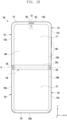
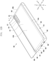
- FIG. 1A is a front perspective view of an electronic device in a flat or unfolded state according to various embodiments of the disclosure.
- FIG. 1B is a diagram illustrating the front of the electronic device in an unfolded state according to various embodiments.
- FIG. 1C is a diagram illustrating the back of the electronic device in an unfolded state according to various embodiments.
- the electronic device 100 may include a flexible display 400 (e.g., foldable display) disposed in an area formed by the pair of housings 110 and 120.
- the first housing 110 and the second housing 120 may be disposed on both sides about the folding axis (axis A), and may have a substantially symmetrical shape with respect to the folding axis (axis A).
- the angle or distance between the first housing 110 and the second housing 120 may vary, depending on whether the state of the electronic device 100 is a flat or unfolded state, a folded state, or an intermediate state.
- the pair of housings 110 and 120 may include a first housing 110 (e.g., first housing structure) coupled to the hinge mechanism (e.g., hinge mechanism 140 in FIG. 1B ), and a second housing 120 (e.g., second housing structure) coupled to the hinge mechanism (e.g., hinge mechanism 140 in FIG. 1B ).
- the first housing 110 in the unfolded state, may include a first surface 111 facing a first direction (e.g., front direction) (z-axis direction), and a second surface 112 facing a second direction (e.g., rear direction) (negative z-axis direction) opposite to the first surface 111.
- the electronic device 100 may be operated in such a manner that the second surface 112 of the first housing 110 and the fourth surface 122 of the second housing 120 face substantially the same second direction (negative z-axis direction) in the unfolded state, and the second surface 112 and the fourth surface 122 face one another in opposite directions in the folded state.
- the second surface 112 may face the first direction (z-axis direction)
- the fourth surface 122 may face the second direction (negative z-axis direction).
- the first housing 110 may include a first side member 113 that at least partially forms an external appearance of the electronic device 100, and a first rear cover 114 coupled to the first side member 113 that forms at least a portion of the second surface 112 of the electronic device 100.
- the first side member 113 may include a first side surface 113a, a second side surface 113b extending from one end of the first side surface 113a, and a third side surface 113c extending from the other end of the first side surface 113a.
- the first side member 113 may be formed in a rectangular shape (e.g., square or rectangle) through the first side surface 113a, second side surface 113b, and third side surface 113c.
- the second housing 120 may include a second side member 123 that at least partially forms the external appearance of the electronic device 100, and a second rear cover 124 coupled to the second side member 123, forming at least a portion of the fourth surface 122 of the electronic device 100.
- the second side member 123 may include a fourth side surface 123a, a fifth side surface 123b extending from one end of the fourth side surface 123a, and a sixth side surface 123c extending from the other end of the fourth side surface 123a.
- the second side member 123 may be formed in a rectangular shape through the fourth side surface 123a, fifth side surface 123b, and sixth side surface 123c.
- the second side surface 113b of the first side member 113 and the fifth side surface 123b of the second side member 123 may be connected without a gap formed therebetween.
- the third side surface 113c of the first side member 113 and the sixth side surface 123c of the second side member 123 may be connected without a gap formed therebetween.
- the electronic device 100 in the unfolded state, may be configured such that the combined length of the second side surface 113b and the fifth side surface 123b is longer than the combined length of the first side surface 113a and/or the fourth side surface 123a.
- the combined length of the third side surface 113c and the sixth side surface 123c may be configured to be longer than the length of the first side surface 113a and/or the fourth side surface 123a.
- the device 100 in the unfolding state, the device 100 may be configured such that the sum of the lengths of the second side surface 113b and the fifth side surface 123b is shorter than or equal to the length of the first side surface 113a and/or the fourth side surface 123a.
- the sum of the lengths of the third side surface 113c and the sixth side surface 123c may be configured to be shorter than or equal to the length of the first side surface 113a and/or the fourth side surface 123a.
- the first side member 113 and/or the second side member 123 may be formed of a metal, and may further include a polymer injected into the metal.
- the first side member 113 and/or the second side member 123 may include at least one conductive portion 116 and/or 126 electrically segmented through one or more segmenting portions 1161 and 1162 and/or segmenting 1261 and 1262, which may be formed using a polymer.
- the at least one conductive portion may be electrically connected to a wireless communication circuit included in the electronic device 100, and may be used as an antenna operating in at least one designated band (e.g., legacy band).
- the first rear cover 114 and/or the second rear cover 124 may be formed of, for example, coated or tinted glass, ceramic, polymer, metal (e.g., aluminum, stainless steel or "STS", or magnesium), or a combination thereof.
- the flexible display 400 may be disposed to extend from the first surface 111 of the first housing 110 across the hinge mechanism (e.g., hinge mechanism 140 in FIG. 1B ) to at least a portion of the third surface 121 of the second housing 120.
- the flexible display 400 may include a first region 130a substantially corresponding to the first surface 111, a second region 130b corresponding to the second surface 121, and a third region 130c (e.g., the bendable region) connecting the first region 130a and the second region 130b and corresponding to the hinge mechanism (e.g., hinge mechanism 140 in FIG. 1B ).
- the electronic device 100 may include a first protection cover 115 (e.g., first protection frame or first decoration member) coupled along the periphery of the first housing 110.
- the electronic device 100 may include a second protection cover 125 (e.g., second protection frame or second decoration member) coupled along the periphery of the second housing 120.
- the first protection cover 115 and/or the second protection cover 125 may be formed of a metal or polymer material.
- the first protection cover 115 and/or the second protection cover 125 may be used as a decorative member.
- the flexible display 400 may be positioned such that the periphery of the first region 130a is interposed between the first housing 110 and the first protection cover 115. According to an embodiment, the flexible display 400 may be positioned such that the periphery of the second region 130b is interposed between the second housing 120 and the second protection cover 125. According to an embodiment, the flexible display 400 may be positioned such that the periphery of the flexible display 400 corresponding to a protection cap 135 is protected through the protection cap disposed in a region corresponding to the hinge mechanism (e.g., hinge mechanism 140 in FIG. 1B ). Consequently, the periphery of the flexible display 400 may be substantially protected from the outside.
- the hinge mechanism e.g., hinge mechanism 140 in FIG. 1B
- the electronic device 100 may include a hinge housing 141 (e.g., hinge cover) that is disposed so as to support the hinge mechanism (e.g., hinge mechanism 140 in FIG. 1B ).
- the hinge housing 141 may further be exposed to the outside when the electronic device 100 is in the folded state, and be invisible as viewed from the outside when retracted into a first space (e.g., internal space of the first housing 110 ) and a second space (e.g., internal space of the second housing 120) when the electronic device 100 is in the unfolded state.
- the flexible display 400 may be disposed to extend from at least a portion of the second surface 112 to at least a portion of the fourth surface 122. In this case, the electronic device 100 may be folded so that the flexible display 400 is exposed to the outside (out-folding scheme).
- the electronic device 100 may include a sub-display 131 disposed separately from the flexible display 400.
- the sub-display 131 may be disposed to be at least partially exposed on the second surface 112 of the first housing 110, and may display status information of the electronic device 100 in place of the display function of the flexible display 400 in case of the folded state.
- the sub-display 131 may be disposed to be visible from the outside through at least some region of the first rear cover 114.
- the sub-display 131 may be disposed on the fourth surface 122 of the second housing 120. In this case, the sub-display 131 may be disposed to be visible from the outside through at least some region of the second rear cover 124.
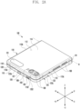
- the electronic device 100 may include at least one of an input device 103 (e.g., microphone), sound output devices 101 and 102, a sensor module 104, camera devices 105 and 108, a key input device 106, or a connector port 107.
- the input device 103 e.g., microphone
- sound output devices 101 and 102, sensor module 104, camera devices 105 and 108, key input device 106, and connector port 107 indicate a hole or shape formed in the first housing 110 or the second housing 120, but may be defined to include a substantial electronic component (e.g., input device, sound output device, sensor module, or camera device) that is disposed inside the electronic device 100 and operated through a hole or a shape.
- the input device 103, the sound output devices 101 and 102, and the connector port 107 may be disposed in a space arranged in the first housing 110 and/or the second housing 120 of the electronic device 100, and may be exposed to the external environment through at least one hole formed in the first housing 110 and/or the second housing 120.
- at least one connector port 107 may be used to transmit and receive power and/or data to and from an external electronic device.
- at least one connector port e.g., ear jack hole
- the sensor module 104 may include at least one of a gesture sensor, a gyro sensor, a barometric pressure sensor, a magnetic sensor, an acceleration sensor, a grip sensor, a color sensor, an infrared (IR) sensor, a biometric sensor, a temperature sensor, a humidity sensor, an illuminance sensor, a proximity sensor, a biometric sensor, an ultrasonic sensor, or an illuminance sensor 104.
- a gesture sensor e.g., a gyro sensor, a barometric pressure sensor, a magnetic sensor, an acceleration sensor, a grip sensor, a color sensor, an infrared (IR) sensor, a biometric sensor, a temperature sensor, a humidity sensor, an illuminance sensor, a proximity sensor, a biometric sensor, an ultrasonic sensor, or an illuminance sensor 104.
- a gesture sensor e.g., a gyro sensor, a barometric pressure sensor, a magnetic sensor,
- the electronic device 100 may be operated to remain in an intermediate state through the hinge mechanism (e.g., hinge device 140 in FIG. 1B ).
- the electronic device 100 may control the flexible display 400 to display different pieces of content on the display area corresponding to the first surface 111 and the display area corresponding to the third surface 121.
- the electronic device 100 may be operated substantially in an unfolded state (e.g., unfolded state of FIG. 1A ) and/or substantially in a folded state (e.g., folded state of FIG.
- the electronic device 100 may include a first side member 113 (e.g., first side frame), a second side member 123 (e.g., second side frame), and a hinge mechanism 140 (e.g., hinge module) rotatably connecting the first side member 113 and the second side member 123.
- the electronic device 100 may include a first support member 1131 (e.g., first support member) at least partially extending from the first side member 113, and a second support member 1231 at least partially extending from the second side member 123.
- the first support member 1131 may be integrally formed with the first side member 113 or may be structurally coupled to the first side member 113.
- the second support member 1231 may be integrally formed with the second side member 123 or may be structurally coupled to the second side member 123.
- the electronic device 100 may include a flexible display 400 disposed to be supported by the first support member 1131 and the second support member 1231.
- the electronic device 100 may include a first rear cover 114 that is coupled to the first side member 113 and provides a first space between itself and the first support member 1131, and a second rear cover 124 that is coupled to the second side member 123 and provides a second space between itself and the second support member 1231.
- the first side member 113 and the first rear cover 114 may be integrally formed.
- the electronic device 100 may include a first substrate assembly 161 (e.g., main printed circuit board), a camera assembly 163, a first battery 171, or a first bracket 151, arranged in the first space between the first side member 113 and the first rear cover 114.
- the camera assembly 163 may include a plurality of camera devices (e.g., camera devices 105 and 108 in FIGS. 1A and 2A ), and may be electrically connected to the first substrate assembly 161.
- the first bracket 151 may provide a support structure for supporting the first substrate assembly 161 and/or the camera assembly 163, and improved rigidity.
- the electronic device 100 may include a hinge housing 141 (e.g., hinge cover) that supports the hinge mechanism 140 and is disposed so as to be exposed to the outside when the electronic device 100 is in the folded state (e.g., folded state of FIG. 2A ) and be invisible from the outside by being retracted into the first space and/or the second space when the electronic device 100 is in the unfolded state (e.g., unfolded state of FIG. 1A ).
- a hinge housing 141 e.g., hinge cover
- the first support member 1131 may include a first support surface 1131a facing a first direction (z-axis direction), and a second support surface 1131b facing a second direction (negative z-axis direction) opposite to the first direction.
- the second support member 1231 may include a third support surface 1231a facing the first direction, and a fourth support surface 1231b facing the second direction in the unfolded state.
- the flexible display 400 may be supported by the first support surface 1131a of the first support member 1131 and the third support surface 1231a of the second support member 1231.
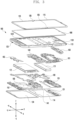
- FIG. 4 is an exploded perspective view of a flexible display according to various embodiments.
- a flexible display 400 may include, for example, and without limitation, an unbreakable (UB) type OLED display (e.g., a curved display).
- UB unbreakable
- the flexible display 400 may include a window layer 410, and a polarizing layer (polarizer (POL)) 420 (e.g., a polarizing film), a display panel 430, a polymer layer 440, a metal sheet layer 450, and a reinforcing plate 470 which are sequentially disposed on a rear surface of the window layer 410.
- the flexible display 400 may include a digitizer 460 disposed between the polymer layer 440 and the metal sheet layer 450 or between the metal sheet layer 450 and the reinforcing plate 470.
- the window layer 410, the polarizing layer 420, the display panel 430, the polymer layer 440, and the metal sheet layer 450 may be disposed to cross at least a part of a first surface (e.g., the first surface 111 of FIG. 1A ) of a first housing (e.g., the first housing 110 of FIG. 1A ) and a third surface (e.g., the third surface 121 of FIG. 1A ) of a second housing (e.g., the second housing 120 of FIG. 1A ).
- the reinforcing plate 470 may include a first reinforcing plate 471 facing the first housing (e.g., the first housing 110 of FIG.
- the window layer 410, the polarizing layer 420, the display panel 430, the polymer layer 440, the metal sheet layer 450, and the reinforcing plate 470 may be attached to each other through adhesive agents P1, P2, P3, and P4 (or adhesives).
- the adhesive agents P1, P2, P3, and P4 may include at least one of an optical clear adhesive (OCA), a pressure sensitive adhesive (PSA), a heat-reactive adhesive, a general adhesive, or a double-sided tape.
- the display panel 430 may include a plurality of pixels and a wiring structure (e.g., an electrode pattern).
- the polarizing layer 420 may selectively pass light generated from a light source of the display panel 430 and vibrating in a predetermined direction.
- the display panel 430 and the polarizing layer 420 may be integrally configured.
- the flexible display 400 may include a touch panel (not shown).
- the metal sheet layer 450 may be configured to have a shape which provides flexibility to the flexible display 400.
- the metal sheet layer 450 may include at least one of steel use stainless (SUS) (e.g., stainless steel (STS)), Cu, Al, or a metal CLAD (e.g., a laminated member in which SUS and Al are alternately disposed).
- the metal sheet layer 450 may include a first plane portion 451 corresponding to the first housing (e.g., the first housing 110 of FIG. 1A ), a second plane portion 452 corresponding to the second housing (e.g., the second housing 120 of FIG.
- the bending portion 453 may include a plurality of openings 4531 arranged at a predetermined (e.g., specified) interval.
- the bending characteristics of the bending portion 453 may be determined throughat least one of a size, a shape, or an arrangement density of at least a part of the plurality of openings 4531.
- the metal sheet layer 450 may include other alloy materials. In various embodiments, the metal sheet layer 450 may help toreinforce the stiffness of an electronic device (e.g., the electronic device 100 of FIG.
- the flexible display 400 may include the digitizer 460 as a detection member which is disposed under the metal sheet layer 450 and receives an input of an electronic pen (e.g., a stylus).
- the digitizer 460 may include a coil member disposed on a dielectric substrate to detect a resonance frequency of an electromagnetic induction scheme applied from the electronic pen.
- the flexible display 400 may include at least one functional member (not shown) disposed between the polymer layer 440 and the metal sheet layer 450 or disposed under the metal sheet layer 450.
- the functional member may include a graphite sheet for heat dissipation, an added display, a force touch FPCB, a fingerprint sensor FPCB, an antenna radiator for communication, or a conductive/nonconductive tape.
- the functional member when bending is impossible, may be separately disposed in the first housing (e.g., the first housing 110 of FIG. 1A ) and the second housing (e.g., the second housing 120 of FIG. 1A ).
- the functional member when bending is possible, may be disposed from the first housing (e.g., the first housing 110 of FIG. 1A ) to at least a part of the second housing (e.g., the second housing 120 of FIG. 1A ) through a hinge device (e.g., the hinge device 140 of FIG. 1B ).
- first housing e.g., the first housing 110 of FIG. 1A
- second housing e.g., the second housing 120 of FIG. 1A
- a hinge device e.g., the hinge device 140 of FIG. 1B
- the electronic device may be disposed under the flexible display 400 and may include a camera device (e.g., the first camera device 105 of FIG. 1A ) configured to detect an external environment through the flexible display 400.
- the electronic device e.g., the electronic device 100 of FIG. 1A
- may include at least one sensor module e.g., the sensor module 104 of FIG. 1A ) (e.g., an illuminance sensor, a proximity sensor, or a TOF sensor) disposed under the flexible display 400.
- the polarizing layer 420, the display panel 430, the polymer layer 440, the metal sheet layer 450, the digitizer 460, and the reinforcing plate 470 may include through-holes 4201, 4301, 4401, 4501, 4601, and 4701.
- the display panel 430 and/or the polarizing layer 420 may not need the through-holes 4201 and 4301 by adjusting the transmittance of a corresponding region.
- the sizes of the through-holes 4201, 4301, 4401, 4501, 4601, and 4701 may be configured based on the size of the camera device (e.g., the first camera device 105 of FIG. 1A ) and/or an angle of view of the camera device (e.g., the first camera device 105 of FIG. 1A ), and the through-holes 4201, 4301, 4401, 4501, 4601, and 4701 may have different sizes.
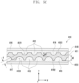
- the window layer 410 may include a glass layer (e.g., a glass layer 411 of FIG. 5C ).
- the glass layer e.g., the glass layer 411 of FIG. 5C
- the glass layer may include a plurality of patterns (e.g., a plurality of patterns 412 and 413 of FIG. 5C ) disposed in a region corresponding to a third bendable portion (e.g., thethird portion 130c of FIG. 1B ) of the flexible display 400 and configured to be lower than the outer surface of the glass layer (e.g., the glass layer 411 of FIG. 5C ), and thus help to improve flexibility of the flexible display 400.
- an etching amount is differently configured for each region in the plurality of patterns (e.g., the plurality of patterns 412 and 413 of FIG. 5C ), thereby helping to provide efficient flexibility corresponding to the folding or bending characteristics of the flexible display.
- window layer 410 will be described in greater detail.
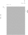
- FIG. 5A is a diagram illustrating the window layer according to various embodiments.
- FIG. 5B is an enlarged perspective view illustrating a region 5b of FIG. 5A according to various embodiments.
- FIG. 5C is a partial cross-sectional view of the window layer viewed along line 5c-5c of FIG. 5A according to various embodiments.
- the window layer 410 may include a first region 410a corresponding to a first housing (e.g., the first housing 110 of FIG. 1A ) of an electronic device (e.g., the electronic device 100 of FIG. 1A ), a second region 410b corresponding to a second housing (e.g., the second housing 120 of FIG. 1A ), and a third region 410c corresponding to a hinge device (e.g., the hinge device 140 of FIG. 1B ).
- the third region 410c may be deformed to be bendable together with a display panel (e.g., the display panel 430 of FIG. 4 ) according to a folding operation of the electronic device (e.g., the electronic device 100 of FIG. 1A ) with reference to a folding axis A.
- the thickness of the glass layer 411 may range from, for example, about 50 ⁇ m to about 300 ⁇ m.
- the glass layer 411 may be configured such that a vertical distance from the first surface 4101 to the second surface 4102 has a thickness in the range of, for example, about 50 ⁇ m to 300 ⁇ m.
- the glass layer 411 may be configured to have a thickness of, for example, about 200 ⁇ m.
- the glass layer 411 may include, on the first surface 4101, a plurality of first patterns 412 configured to be lower than the first surface 4101 and spaced apart from each other at a predetermined interval.
- the glass layer 411 may include, on the second surface 4102, a plurality of second patterns 413 configured to be lower than the second surface 4102 and spaced apart from each other at a predetermined interval.
- the plurality of first patterns 412 and the plurality of second patterns 413 may be disposed in regions corresponding to the first region 410a, the second region 410b, and the third region 410c of the window layer 410 in the glass layer 411.
- the plurality of first patterns 412 and the plurality of second patterns 413 may be formed through a process such as etching or laser. According to an embodiment, the plurality of first patterns 412 and the plurality of second patterns 413 may be configured to have lengths in a first direction (e.g., a -x-axis direction) parallel to the folding axis A. In various embodiments, the plurality of first patterns 412 and the plurality of second patterns 413 may be configured to have lengths in a direction not parallel to the folding axis A.
- a first direction e.g., a -x-axis direction
- the plurality of first patterns 412 and the plurality of second patterns 413 may be configured to have lengths in a direction not parallel to the folding axis A.
- each of the plurality of first patterns 412 and the plurality of second patterns 413 may be configured to have a straight line shape, a curved shape, a mixed shape of a straight line and a curved line, or a zigzag shape in which straight lines and/or curved lines extend alternately in opposite directions at specified lengths.
- the plurality of first patterns 412 and the plurality of second patterns 413 may be generally configured to have a hemispherical cross section, but are not limited thereto, and may be configured to have, for example, a rectangular, oval, or polygonal cross section.
- the plurality of first patterns 412 may be configured through first grooves 4121 configured to be lower (e.g., deeper) than the first surface 4101.
- the plurality of second patterns 413 may be configured through second grooves 4131 configured to be lower (e.g., deeper) than the second surface 4102.
- the plurality of first patterns 412 may be configured such that a shortest distance d2 from the first grooves 4121 to the second surface 4102 has a range of, for example, about 10 ⁇ m to 100 ⁇ m.
- the shortest distance d2 from the first grooves 4121 to the second surface 4102 may be formed to have a depth of, for example, at least 30 ⁇ m, and thus help to secure the stiffness of the glass layer 411.
- the plurality of second patterns 413 may be configured such that a shortest distance d1 from the second grooves 4131 to the first surface 4101 has a range of, for example, about 10 ⁇ m to 100 ⁇ m.
- the shortest distance d1 from the second grooves 4131 to the first surface 4101 may be formed to have a depth of, for example, at least 30 ⁇ m, and thus help to secure the stiffness of the glass layer 411.
- the plurality of first patterns 412 and the plurality of second patterns 413 may be configured such that a shortest distance d between at least one pattern among the plurality of first patterns 412 and at least one pattern adjacent thereto among the plurality of second patterns 413 has a range of, for example, about 10 ⁇ m to 100 ⁇ m.
- the shortest distance d between at least one pattern among the plurality of first patterns 412 and at least one pattern adj acent thereto among the plurality of second patterns 413 may be configured to be, for example, at least 30 ⁇ m, and thus help to secure the stiffness of the glass layer 411.
- the feature in which the glass layer 411 includes, on the first surface 4101, the plurality of first patterns 412 configured to be lower than the first surface 4101 may refer, for example, to the plurality of first patterns 412 being disposed at a position in the opposite direction (a -Z-axis direction) of a direction in which the first surface 4101 faces.
- the feature in which the glass layer 411 includes, on the second surface 4102, the plurality of second patterns 413 configured to be lower than the second surface 4102 may refer, for example, to the plurality of second patterns 413 being disposed at a position in the opposite direction (anZ-axis direction) of a direction in which the second surface 4102 faces.
- the glass layer 411 may include only one plurality of patterns between the plurality of first patterns 412 formed on the first surface 4101 and/or the plurality of second patterns 413 formed on the second surface 4102.
- the glass layer 411 may include only the plurality of first patterns 412.
- the glass layer may include only the plurality of second patterns 413.
- the filling members 414 and 415 may include a material which is filled in the grooves 4121 and 4131 of the plurality of patterns 412 and 413 in an initial liquid or semi-solid form, and then cured through time elapsing, irradiation with light, or chemical treatment.
- the filling members 414 and 415 may include a resin such as silicone, urethane, or acrylic.
- the filling members 414 and 415 may include a material having substantially the same refractive index as that of the glass layer 411, and thus induce the plurality of patterns 412 and 413 to be visually invisible from the outside.
- the filling members 414 and 415 disposed at positions corresponding to the first region 410a and the second region 410b of the window layer 410 and the filling members 414 and 415 disposed in a region corresponding to the third region 410c may include different materials.
- a medium having a relatively high elastic modulus may be used.
- the window layer 410 may include a first planarization layer 4141 laminated on the first surface 4101 of the glass layer 411, and a second planarization layer 4151 laminated on the second surface 4102 of the glass layer 411.
- the first planarization layer 4141 may be disposed between the first surface 4101 of the glass layer 411 and the protective layer 416.
- the second planarization layer 4151 may be disposed between the second surface 4102 of the glass layer 411 and the impact absorbing layer 417.
- the first planarization layer 4141 and/or the second planarization layer 4151 may be omitted.
- the first planarization layer 4141 and the second planarization layer 4151 may be formed of a material different from the filling members 414 and 415. According to an embodiment, the first planarization layer 4141 and the second planarization layer 4151 may be formed to have a thickness in a range of, for example, 10 ⁇ m to 100 ⁇ m. For example, the first planarization layer 4141 and the second planarization layer 4151 may be formed to have a thickness of, for example, about 10 ⁇ m.
- the glass layer 411 may include the plurality of patterns 412 and 413 formed in substantially the same manner not only in the third region 410c of the window layer 410 but also in parts corresponding to the first region 410a and the second region 410b, so that a phenomenon in which only the third region 410c is visually recognized from the outside may be reduced.
- the glass layer 411 may be formed to have a relatively thick thickness that is advantageous for stiffness reinforcement, while providing improved bending characteristics to a part corresponding to at least the third region 410c of the window layer 410 through the plurality of patterns 412 and 413.
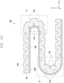
- FIG. 5D is a partial cross-sectional view of the glass layer, according to various embodiments.
- the glass layer 411 may include the plurality of first patterns 412 formed on the first surface 4101 to be lower than the first surface 4101 and arranged at a predetermined interval, and the plurality of second patterns 413 formed on the second surface 4102 to be lower than the second surface 4102 and arranged at a predetermined interval.
- the glass layer 411 may include first etched portions EA1 (e.g., first etched portions) formed on the first surface 4101 through the plurality of first patterns 412 and having a first area, and first non-etched portions A1 (e.g., first non-etched portions) which are not etched.
- the glass layer 411 may include second etched portions EA2 (e.g., second etched portions) formed on the second surface 4102 through the plurality of second patterns 413 and having a second area, and second non-etched portions A2 (e.g., second non-etched portions) which are not etched.
- the glass layer 411 in the case of being applied to an electronic device (e.g., the electronic device 100 of FIG. 1A ) operating in an in-folding manner, the glass layer 411 may be configured such that the first area of the first etched portions EA1 is smaller than the second area of the second etched portions EA2.
- the area of the first non-etched portions A1 may be configured to be larger than the area of the second non-etched portions A2.
- FIGS. 6A , 6B and 6C are partial cross-sectional views of the glass layer illustrating a shape and an arrangement structure of the plurality of patterns according to various embodiments.
- the glass layer 411 may include the plurality of first patterns 412 disposed on the first surface 4101 and the plurality of second patterns 413 disposed on the second surface 4102.
- the plurality of first patterns 412 and the plurality of second patterns 413 may be disposed in a manner in which a first virtual line L1 passing through the center of each of the plurality of first patterns 412 does not coincide with a second virtual line L2 passing through the center of each of the plurality of second patterns 413.
- a staggered (e.g., at least partially non-overlapping) arrangement structure of the plurality of first patterns 412 and the plurality of second patterns 413 may help to improve the stiffness of the glass layer 411.
- the glass layer 411 may include the plurality of first patterns 412 disposed on the first surface 4101 and the plurality of second patterns 413 disposed on the second surface 4102.
- the virtual line passing through the center of each of the plurality of second patterns 413 may be disposed in a manner consistent with the virtual line L1 passing through the center of each of the plurality of first patterns 412.
- a matched (e.g., overlapping) arrangement structure of the plurality of first patterns 412 and the plurality of second patterns 413 may help to improve the flexibility of the glass layer 411.
- the glass layer 411 may include the plurality of patterns 412 and 413 in which the configuration of FIG. 6A and the configuration of FIG.
- the glass layer 411 may include the plurality of first patterns 412 disposed on the first surface 4101 and the plurality of second patterns 413 disposed on the second surface 4102.
- each of the plurality of first patterns 412 may include the first groove 4121 having a predetermined depth and formed to be lower than the first surface 4101.
- the first groove 4121 may be configured in a manner in which an etching area of the first groove increases as it progresses from the first surface 4101 to the second surface 4102.
- the first groove 4121 may include an introduction portion having a first width W1 and formed on the first surface 4101 and an internal space having a second width W2 wider than the introduction portion.
- the first groove 4121 may be formed through an isotropic etching process.
- the second groove 4131 included in each of the plurality of second patterns 413 may also be formed in substantially the same manner as the first groove 4121.
- the glass layer 411 formed through the first and second patterns 412 and 413 including the grooves 4121 and 4131 having such a shape may help to improve the flexibility through an increase in the amount of etching, and the first surface 4101 and the second surface 4102 have relatively large areas, so that the stiffness (e.g., pressure-resistant properties) of the glass layer may be improved.
- the glass layer 411 having high stiffness compared to improved flexibility may help to improve the use convenience of an electronic pen operated in a manner that the same is in contact with the first surface.
- FIG. 7A is a flowchart illustrating an example manufacturing process of the window layer according to various embodiments.
- FIG. 7B is a diagram illustrating an example process for manufacturing the window layer according to various embodiments.
- a glass base material 411' may be arranged.
- the glass base material 411' may protect a display and may be configured to have a thickness having pressure-resistant properties according to a contact with an external electronic device (e.g., an electronic pen).
- the thickness of the glass base material 411' may have a range of about 100 ⁇ m to 500 ⁇ m.
- a photoresist layer 721 may be disposed on each of both surfaces of the glass base material 411' as shown in case (a) of FIG. 7B .
- the photoresist layers 721 may be formed in such a manner in which a photoresist is applied or coated.
- the photoresist may include a resin which undergoes a chemical change when irradiated with light of a specific wavelength, and may cause a change of dissolution and solidification in response to specific light, from ultraviolet to visible wavelengths.
- a soft bake process may be performed on the glass base material 411' at a specified temperature.
- the masking member 722 may include patterns having shapes corresponding to the plurality of first patterns 412 and the plurality of second patterns 413 to be formed on the glass layer 411. Accordingly, through the exposure process, a part of the photoresist layer 721 corresponding to the plurality of first and second patterns 412 and 413 and any one of the other parts thereof may be exposed through light.
- a specific wavelength e.g., ultraviolet light
- the masking member 722 may be removed, and an exposed photoresist layer 7211 may be developed through a developing solution.
- an exposed photoresist layer 7211 may be developed through a developing solution.
- a corresponding region of the exposed photoresist layer 7211 corresponding to the plurality of first and second patterns exposed to light through the masking member 722 is removed, so that the outer surface of the glass base material 411' may be exposed.
- the glass base material 411' from which at least a part of the partially exposed photoresist layer 7211 is removed may be formed as the glass layer 411 having the plurality of first patterns 412 and the plurality of second patterns 413 including grooves having a specified depth and area from the outer surface of the glass base material 411', through etching.
- the plurality of first patterns 412 and the plurality of second patterns 413 may be formed through isotropic etching or anisotropic etching.
- a residual photoresist layer 7211 applied to the outer surface of the glass layer 411 through a post-processing process may be removed, and a filling member (e.g., the filling members 414 and 415 of FIG. 5C ) and a protective layer (e.g., the protective layer 416 or the impact absorbing layer 417 of FIG. 5C ) may be additionally laminated thereon.
- a filling member e.g., the filling members 414 and 415 of FIG. 5C
- a protective layer e.g., the protective layer 416 or the impact absorbing layer 417 of FIG. 5C
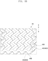
- FIGS. 8A and 8B are diagrams illustrating example views of the glass layer including the plurality of patterns according to various embodiments.
- the plurality of first patterns 412 formed on the glass layer 411 may be formed to have a length in a direction parallel to the folding axis A through the grooves 4121, so as to improve the flexibility.
- the plurality of first patterns 412 may be configured to have a zigzag shape bent by alternating opposite directions at a specified angle for each length specified in a straight line shape.
- the plurality of first patterns 412 in a similar manner, may be configured to have a curved shape or a mixed shape of a straight line and a curved line.
- a plurality of second patterns e.g., the plurality of second patterns 413 of FIG. 5C
- a second surface e.g., the second surface 4102 of FIG. 5C
- the glass layer 411 may also be configured in substantially the same manner.
- the plurality of first patterns 412 formed on the glass layer 411 may include a plurality of sub-patterns 412a, 412b, 412c, 412d, 412e, and 412f which are arranged along a direction parallel to the folding axis A.
- the plurality of sub-patterns 412a, 412b, 412c, 412d, 412e, and 412f may be formed to have a specified length and to be inclined at a specified angle.
- the plurality of sub-patterns 412a, 412b, 412c, 412d, 412e, and 412f may be alternately formed to be inclined at angles indirections opposite to each other.
- the plurality of sub-patterns 412a, 412b, 412c, 412d, 412e, and 412f may also be configured to have a straight line shape of a direction parallel to the folding axis A.
- a plurality of second patterns e.g., the plurality of second patterns 413 of FIG. 5C
- a second surface e.g., the second surface 4102 of FIG. 5C
- the glass layer 411 may also be configured in substantially the same manner.
- FIGS. 9A and 9B are partial cross-sectional views illustrating a shape and an arrangement configuration of the plurality of patterns according to a bending direction of the display panel according to various embodiments.
- the glass layer 411 may include the first surface 4101 and the second surface 4102 facing in a direction opposite to the first surface 4101 and corresponding to the display panel 430. According to an embodiment, the glass layer 411 may include, on the first surface 4101, the plurality of first patterns 412 configured at a predetermined interval to be lower than the first surface 4101. According to an embodiment, the glass layer 411 may include, on the second surface 4102, the plurality of second patterns 413 configured at a predetermined interval to be lower than the second surface 4102.
- an etching amount per unit area of the plurality of first patterns 412 and an etching amount per unit area of the plurality of second patterns 413 may be configured differently according to a folding manner of an electronic device.
- the etching amount per unit area may be determined through an etching depth, an etching interval, or an etching area of the patterns 412 and 413. For example, as shown in FIG.
- the glass layer 411 may be configured such that the etching amount per unit area of the plurality of second patterns 413 disposed on the second surface 4102 is larger than the etching amount per unit area of the plurality of first patterns 412 disposed on the first surface 4101, and thus help to improve the flexibility.
- the etching amount per unit area of the plurality of second patterns 413 disposed on the second surface 4102 is larger than the etching amount per unit area of the plurality of first patterns 412 disposed on the first surface 4101, and thus help to improve the flexibility.
- the glass layer 411 may be configured such that a shortest distance from the first surface 4101 to the second surface 4102 may, for example, be at most 300 ⁇ m or less. According to an embodiment, the glass layer 411 may be configured such that a shortest distance (e.g., the shortest distance d2 of FIG. 5C ) from each of the plurality of first patterns 412 to the second surface 4102, a shortest distance (e.g., the shortest distance d1 of FIG. 5C ) from each of the plurality of second patterns 413 to the first surface 4101, or a shortest distance (e.g., the shortest distance d of FIG. 5C ) between each of the plurality of first patterns 412 and each of the plurality of second patterns 413 adjacent thereto has a range of, for example, about 50 ⁇ m to 150 ⁇ m.
- FIG. 10 is a diagram illustrating an example window layer according to various embodiments.
- window layer 410 of FIG. 10 components substantially the same as or similar to those of the window layer 410 of FIG. 5A are given the same reference numerals, and a detailed description thereof may not be repeated.
- the window layer 410 may include the first region 410a corresponding to a first housing (e.g., the first housing 110 of FIG. 1A ) of an electronic device (e.g., the electronic device 100 of FIG. 1A ), the second region 410b corresponding to a second housing (e.g., the second housing 120 of FIG. 1A ), and the third region 410c corresponding to a hinge device (e.g., the hinge device 140 of FIG. 1B ).
- the third region 410c may be deformed to be bendable together with a display panel (e.g., the display panel 430 of FIG. 4 ) according to a folding operation of the electronic device (e.g., the electronic device 100 of FIG. 1A ) with reference to the folding axis A.
- the window layer 410 may include the glass layer 411 disposed in a part corresponding to the third region 410c and including the plurality of first patterns 412 and the plurality of second patterns 413 disposed on a front surface (e.g., the first surface 4101 of FIG. 5C ) and a rear surface (e.g., the second surface 4102 of FIG. 5C ), respectively, so as to help to improve the flexibility of the window layer 410.
- the plurality of patterns 412 and 413 may be omitted in a part corresponding to the first region 410a of the window layer 410 and in a part corresponding to the second region 410b, thereby helping to reinforce the stiffness of the window layer 410.
- an electronic device 500 may include a first housing 510, a second housing 520, and a third housing 530 which are rotatably disposed with respect to each other.
- the electronic device 500 may include a flexible display 540 disposed to be supported by the first housing 510, the second housing 520, and the third housing 530.
- the first housing 510 and the second housing 520 may be rotatably connected to each other with reference to a first folding axis X1 through a first hinge device 561.
- the second housing 520 and the third housing 530 may be rotatably connected to each other with reference to a second folding axis X2 through a second hinge device 562.
- the first housing 510 may include a first surface 511, a second surface 512 facing in a direction opposite to the first surface 511, and a first side surface member 513 surrounding the space between the first surface 511 and the second surface 512.
- the second housing 520 may include a third surface 521, a fourth surface 522 facing in a direction opposite to the third surface 521, and a second side surface member 523 surrounding the space between the third surface 521 and the fourth surface 522.
- the third housing 530 may include a fifth surface 531, a sixth surface 532 facing in a direction opposite to the fifth surface 531, and a third side surface member 533 surrounding the space between the fifth surface 531 and the sixth surface 532.
- the flexible display 540 may be disposed to be supported by the first surface 511, the third surface 521, and the fifth surface 531.
- the flexible display 540 may include a glass layer 541 (e.g., the glass layer 411 of FIG. 5C ) which protects a display panel (e.g., the display panel 430 of FIG. 5C ) and is laminated thereon to provide the flexibility.
- the glass layer 541 may include a first region DA1 facing the first housing 510, a second region DA2 facing the second housing 520, and a third region DA3 facing the third housing 530.
- the glass layer 541 may include the first surface 4101 and the second surface 4102 facing in a direction opposite to the first surface 4101 and corresponding to the display panel 430.
- the glass layer 541 may include, on the first surface 4101, the plurality of first patterns 412 configured at a predetermined interval to be lower than the first surface 4101.
- the glass layer 541 may include, on the second surface 4102, the plurality of second patterns 413 configured at a predetermined interval to be lower than the second surface 4102.
- the glass layer 541 may be configured such that an etching amount per unit area of the plurality of second patterns 413 disposed on the second surface 4102 is less than an etching amount per unit area of the plurality of first patterns 412 disposed on the first surface 4101, at least in the first folding region F1, and thus may help to improve the flexibility.
- the glass layer 541 may be configured such that the etching amount per unit area of the plurality of second patterns 413 disposed on the second surface 4102 is larger than the etching amount per unit area of the plurality of first patterns 412 disposed on the first surface 4101, at least in the second folding region F2, and thus may help to improve the flexibility.
- the etching amounts per unit area of the plurality of first patterns 412 disposed on the first surface 4101 of the glass layer 541 and the plurality of second patterns 413 disposed on the second surface 4102 may be appropriately configured according to the different bending manners of the display panel 540, so as to help to improve flexibility.
- the glass layer 541 may be configured such that a shortest distance (e.g., the shortest distance d2 of FIG. 5C ) from each of the plurality of first patterns 412 to the second surface 4102, a shortest distance (e.g., the shortest distance d1 of FIG. 5C ) from each of the plurality of second patterns 413 to the first surface 4101, or a shortest distance (e.g., the shortest distance d of FIG. 5C ) between each of the plurality of first patterns 412 and each of the plurality of second patterns 413 adjacent thereto has a range of, for example, about 10 ⁇ m to 100 ⁇ m, at least in the second folding region F2.
- FIG. 12A is a front perspective view illustrating a slide-out state of an electronic device according to various embodiments.
- FIG. 12B is a rear perspective view illustrating a slide-in state of the electronic device according to various embodiments.
- the bendable member may be at least partially slid into an inner space of the housing 610 while supporting the flexible display 630.
- the electronic device 600 may include the housing 610 (e.g., a housing structure) including a front surface 610a facing a first direction (e.g., a Z-axis direction), a rear surface 610b facing a second direction (a -Z-axis direction) opposite to the first direction, and a side surface member 640 surrounding the space between the front surface 610a and the rear surface 610b and including a side surface 610c at least partially exposed to the outside.
- a housing structure including a front surface 610a facing a first direction (e.g., a Z-axis direction), a rear surface 610b facing a second direction (a -Z-axis direction) opposite to the first direction, and a side surface member 640 surrounding the space between the front surface 610a and the rear surface 610b and including a side surface 610c at least partially exposed to the outside.
- the rear surface 610b may be configured through a rear cover 621 coupled to the housing 610.
- the rear cover 621 may be formed of a polymer, coated or colored glass, ceramic, a metal (e.g., aluminum, stainless steel (STS), or magnesium), or a combination of at least two of the materials.
- the rear cover 621 may be integrally configured with the housing 610.
- at least a part of the side surface 610c may be disposed to be exposed to the outside through the housing 610.
- the slide structure 660 supports the flexible display 630 and is slid out from the second side surface 642 to a direction of the fourth side surface 644 (e.g., an X-axis direction), so that a display area of the flexible display 630 may be expanded, or the slide structure is slid in from the fourth side surface 644 to a direction of the second side surface 642 (e.g., a -X-axis direction), so that the display area of the flexible display 630 may be reduced.
- the electronic device 600 may include a first side surface cover 640a and a second side surface cover 640b for covering the first side surface 641 and the third side surface 643.
- the first side surface 641 and the third side surface 643 may be disposed so as not to be exposed to the outside through the first side surface cover 640a and the second side surface cover 640b.
- the electronic device 600 may include the flexible display 630 disposed to be supported by the slide structure 660.
- the flexible display 630 may include a first portion 630a (e.g., a plane portion) supported by the slide structure 660, and a second portion 630b (e.g., a bending portion or a bendable portion) extending from the first portion 630a and at least partially supported by the bendable member.
- the second portion 630b may be slid into the inner space of the housing 610 and disposed so as not to be exposed to the outside in a slide-in state of the electronic device 600 (e.g., in a state where at least a part of the slide structure 660 is slid into the housing 610), and may be at least partially exposed to the outside so as to extend from the first portion 630a while being supported by at least a part of the bendable member in a slide-out state of the electronic device 600 (e.g., in a state where at least a part of the slide structure 660 is slid out from the housing 610).
- the electronic device 600 may include a rollable type or a slideable type electronic device in which a display area of the flexible display 630 is changed according to the movement of the slide structure 660 from the housing 610.
- the slide structure 660 may be movably coupled in a sliding manner so as to be at least partially slid in or out from the housing 610.
- the flexible display 630 may be configured to have a display area corresponding to a first width W1 from the second side surface 642 to the fourth side surface 644 in a slide-in state.
- in a state where the slide structure 660 is slid out at least a part of the bendable member slid into the housing 610 is moved to the outside of the electronic device to additionally have a second width W2, so that the flexible display 630 may be deformed to have a display area corresponding to a third width W3 larger than the first width W1.
- the flexible display 630 may have a variable display area corresponding to a variable width of the electronic device.
- the electronic device 600 may include at least one of an input device 603, sound output devices 606 and 607, sensor modules 604 and 617, camera modules 605 and 616, a connector port 608, a key input device (not shown), or an indicator (not shown).
- at least one of the above-described components may be omitted or other components may be additionally included.
- the input device 603 may include a microphone. In various embodiments, the input device 603 may include a plurality of microphones arranged to sense a direction of sound.
- the sound output devices 606 and 607 may include speakers.
- the sound output devices 606 and 607 may include an external speaker 606 and a call receiver 607.
- the sound output devices 606 and 607 may include a speaker (e.g., a piezo speaker) which operates while excluding a separate speaker hole.
- the flash 618 may include, for example, a light-emitting diode or a xenon lamp.
- two or more lenses (wide-angle and telephoto lenses) and image sensors may be disposed on one surface of the electronic device 600.
- the electronic device 600 may include at least one antenna (not shown).
- the at least one antenna may wirelessly communicate with an external electronic device or wirelessly transmit/receive power required for charging.
- the antenna may include a legacy antenna, an mmWave antenna, a near field communication (NFC) antenna, a wireless charging antenna, and/or a magnetic secure transmission (MST) antenna.
- NFC near field communication
- MST magnetic secure transmission
- the flexible display 630 may include a glass layer 631 laminated on a display panel (e.g., the display panel 430 of FIG. 5C ).
- the glass layer 631 may include a plurality of patterns (e.g., the plurality of patterns 412 and 413 of FIG. 12C ) formed in a region corresponding to the second portion 630b which is at least partially deformed to be bendable when the slide structure 660 slides in a specified direction (direction (D), and thus help to secure the stiffness and flexibility of the flexible display 630.
- FIG. 12C is a cross-sectional view illustrating a shape and an arrangement configuration of the plurality of patterns according to bending of the flexible display in a bendable region according to various embodiments.
- the glass layer 631 may be configured such that an etching amount per unit area of the plurality of second patterns 413 disposed on the second surface 4102 is larger than an etching amount per unit area of the plurality of first patterns 412 disposed on the first surface 4101 in a region corresponding to at least a part of the second portion 630b of the flexible display 630, and thus may help to improve the flexibility.
- the glass layer 631 may be configured such that a shortest distance from the first surface 4101 to the second surface 4102 may, for example, be at most 300 ⁇ m or less. According to an embodiment, the glass layer 631 may be configured such that a shortest distance (e.g., the shortest distance d2 of FIG. 5C ) from each of the plurality of first patterns 412 to the second surface 4102, a shortest distance (e.g., the shortest distance d1 of FIG. 5C ) from each of the plurality of second patterns 413 to the first surface 4101, or a shortest distance (e.g., the shortest distance d of FIG.
- a shortest distance e.g., the shortest distance d2 of FIG. 5C
- each of the plurality of first patterns 412 and each of the plurality of second patterns 413 adjacent thereto has a range of, for example, about 10 ⁇ m to 100 ⁇ m in a region corresponding to at least the second portion 630b.
- an electronic device may include: a first housing (e.g., the first housing 110 of FIG. 1A ), a second housing (e.g., the second housing 120 of FIG. 1A ) foldably connected to the first housing through a hinge (e.g., the hinge device 140 of FIG. 1B ), and a flexible display (e.g., the flexible display 400 of FIG. 1A ) supported by the first housing and the second housing, the flexible display including a window layer (e.g., the window layer 410 of FIG. 5A ) having a first surface facing a first direction (e.g., the first surface 4101 of FIG.
- a first housing e.g., the first housing 110 of FIG. 1A
- a second housing e.g., the second housing 120 of FIG. 1A
- a hinge e.g., the hinge device 140 of FIG. 1B
- a flexible display e.g., the flexible display 400 of FIG. 1A
- the flexible display including a window layer (e.
- the first etching amount and/or the second etching amount may correspond to an etching depth of the plurality of first patterns and/or the plurality of second patterns.
- the first etching amount and/or the second etching amount may correspond to an etching shape of the plurality of first patterns and/or the plurality of second patterns.
- the first etching amount and/or the second etching amount may correspond to an arrangement density of the plurality of first patterns and/or the plurality of second patterns.
- the window layer may further include a filler filled in the plurality of first patterns and/or the plurality of second patterns.
- the window layer may further include at least one protective layer including a polymer material and laminated on the planarization layer.
- a vertical distance between each unit pattern of the plurality of second patterns and the first surface may be at least 30 ⁇ m.
- the electronic device may be configured to be folded wherein at least parts of the flexible display face in opposite directions (an out-folding type), and the second etching amount may be less than the first etching amount.
- the glass layer includes a plurality of patterns (e.g., the plurality of first patterns 412 or the plurality of second patterns 413 of FIG. 5C ) on the first surface, a surface of the plurality of patterns being lower than the first surface or on the second surface, a surface of the plurality of patterns being lower than the second surface, and the plurality of patterns have a zigzag shape.
Abstract
According to various embodiments, an electronic device may include: a first housing, a second housing foldably connected to the first housing through a hinge, and a flexible display supported by the first housing and the second housing, the flexible display including a window layer having a first surface and a second surface facing a direction opposite to the first surface, and including a glass layer, and a display panel corresponding to the second surface under the window layer, wherein the glass layer includes a plurality of first patterns on the first surface, a surface of the plurality of first patterns being lower than the first surface, and a plurality of second patterns on the second surface, a surface of the plurality of second patterns being lower than the second surface, and a first etching amount per unit area of the plurality of first patterns and a second etching amount per the unit area of the plurality of second patterns are different.
Description
- The disclosure relates to an electronic device including a flexible display.
- Electronic devices have been improved to be slimmer, to have increased rigidity, enhanced design aspects, and to have differentiated functional elements. Electronic devices are evolving from unilateral rectangular shapes to more diversified shapes. Electronic devices may have deformable structures such that large-screen displays are available while being carried conveniently. As examples of the deformable structures, electronic devices may include a foldable electronic device including at least two foldable housings folded or unfolded with regard to each other, a slidable electronic device including housings configured to slide by a designated reciprocating distance with regard to each other, and a rollable electronic device including at least one housing, the shape of which is changed in a rolling manner. Such electronic devices may include a flexible display which is disposed to correspond to housings deformed in various manners, and which has an at least partially bendable area. Such a flexible display may be required to have improved visibility, flexibility, or rigidity.
- An electronic device (for example, foldable electronic device, slidable electronic device, or rollable electronic device) may include a flexible display bendably supported through at least one housing. The flexible display may be disposed such that a display panel is stacked beneath a window layer made of a bendable polymer (for example, polyimide) material, thereby providing flexibility.
- However, the window layer made of a polymer material may have poor transmittance of scratch resistance, although bendability/flexibility may be provided. In an attempt to solve this problem, at least a part of the window layer may be provided as a thin-film glass layer (for example, UTG (ultrathin glass)), but rigidity may be difficult to ensure because the same is formed as a thin film for providing bendability/flexibility. Moreover, the electronic device may include an electronic pen, and may need to include a flexible display having reinforced rigidity such that, when the pen tip of the electronic pen pressurizes the outer surface of the window layer with a constant pressurizing force, the same can be endured.
- Embodiments of the disclosure may provide an electronic device including a flexible display having flexibility secured such that the same can at least partially bend.
- Embodiments of the disclosure may provide an electronic device including a flexible display having secured rigidity, excellent transmittance, and enhanced scratch resistance.
- Embodiments of the disclosure may provide an electronic device including a flexible display configured such that uniform visibility can be secured with regard to a bending part.
- Problems to be addressed by the disclosure are not limited to the above-mentioned problems, and may be variously expanded without deviating from the idea and scope of the disclosure.
- According to various example embodiments, an electronic device may include: a first housing, a second housing foldably connected to the first housing through a hinge, and a flexible display disposed to be supported by the first housing and the second housing, the flexible display including a window layer having a first surface facing a first direction and a second surface facing in a second direction opposite to the first direction, and including a glass layer, and a display panel disposed to correspond to the second surface under the window layer, wherein the glass layer includes a plurality of first patterns on the first surface, a surface of the plurality of first patterns being lower than the first surface, and a plurality of second patterns on the second surface, a surface of the plurality of second patterns being lower than the second surface, wherein a first etching amount per unit area of the plurality of first patterns and a second etching amount per the unit area of the plurality of second patterns are different.
- According to various example embodiments, an electronic device may include: at least one housing, and a flexible display including a bending region which is at least partially bendable through support of the at least one housing, the flexible display including a window layer having a first surface facing a first direction and a second surface facing in a second direction opposite to the first direction, and including a glass layer, and a display panel disposed to correspond to the second surface under the window layer, wherein the glass layer includes a plurality of first patterns on the first surface, a surface of the plurality of first patterns being lower than the first surface, and a plurality of second patterns on the second surface, a surface of the plurality of second patterns being lower than the second surface, and a first etching amount per unit area of the plurality of first patterns and a second etching amount per the unit area of the plurality of second patterns are different.
- According to various example embodiments, an electronic device may include: a first housing, a second housing foldably connected to the first housing through a hinge, and a flexible display disposed to be supported by the first housing and the second housing, the flexible display including a window layer having a first surface facing a first direction and a second surface facing a second direction opposite to the first direction, and including a glass layer, and a display panel disposed to correspond to the second surface under the window layer, wherein the glass layer includes a plurality of patterns on the first surface, the plurality patterns being lower than the first surface or on the second surface, the plurality of patterns being lower than the second surface, and the plurality of patterns have a zigzag shape.
- A flexible display according to various example embodiments of the disclosure may have different etching ratios configured with regard to multiple patterns disposed on oppositely-oriented surfaces of a glass layer, thereby providing efficient flexibility according to bending characteristics of an electronic device. In addition, a glass layer having a sufficient thickness is provided as a part of the window layer, thereby helping to secure rigidity (for example, pressure-resisting characteristics).
- Various other advantageous effects identified explicitly or implicitly through the disclosure may be provided.
- In relation to the description of drawings, the same or similar reference numerals may be used for the same or similar components.
-
FIG. 1A is a front perspective view of an electronic device in an unfolded state according to various embodiments; -
FIG. 1B is a diagram illustrating a front surface of an electronic device in an unfolded state according to various embodiments; -
FIG. 1C is a diagram illustrating a rear surface of an electronic device in an unfolded state according to various embodiments; -
FIG. 2A is a perspective view of an electronic device, in a folded state according to various embodiments; -
FIG. 2B is a perspective view of an electronic device, in an intermediate state according to various embodiments; -
FIG. 3 is an exploded perspective view of an electronic device according to various embodiments; -
FIG. 4 is an exploded perspective view of a flexible display according to various embodiments; -
FIG. 5A is a diagram illustrating an example window layer according to various embodiments; -
FIG. 5B is an enlarged perspective view illustrating a region ofFIG. 5A according to various embodiments; -
FIG. 5C is a partial cross-sectional view of a window layer taken along line 5c-5c ofFIG. 5A according to various embodiments; -
FIG. 5D is a partial cross-sectional view of a glass layer, according to various embodiments; -
FIGS. 6A ,6B and6C are partial cross-sectional views of a glass layer illustrating a shape and an arrangement structure of a plurality of patterns according to various embodiments; -
FIG. 7A is a flowchart illustrating an example manufacturing process of a window layer according to various embodiments; -
FIG. 7B is a diagram illustrating an example process for manufacturing a window layer according to various embodiments; -
FIGS. 8A and8B are diagrams illustrating example glass layers including a plurality of patterns according to various embodiments; -
FIGS. 9A and9B are cross-sectional views illustrating a shape and an arrangement configuration of a plurality of patterns according to a bending direction of a display panel according to various embodiments; -
FIG. 10 is a diagram illustrating a window layer according to various embodiments; -
FIG. 11A is a diagram illustrating an electronic device, in an unfolded state according to various embodiments; -
FIG. 11B is a sectional view illustrating an electronic device ofFIG. 11A in a folded state according to various embodiments; -
FIG. 11C is a sectional view illustrating a shape and an arrangement of a plurality of patterns according to a bending direction of a flexible display ofFIG. 11A according to various embodiments; -
FIG. 12A is a front perspective view illustrating a slide-out state of an electronic device according to various embodiments; -
FIG. 12B is a rear perspective view illustrating a slide-out state of an electronic device according to various embodiments; and -
FIG. 12C is a sectional view illustrating a shape and an arrangement configuration of a plurality of patterns according to bending of a flexible display in a bendable region according to various embodiments. -
FIG. 1A is a front perspective view of an electronic device in a flat or unfolded state according to various embodiments of the disclosure.FIG. 1B is a diagram illustrating the front of the electronic device in an unfolded state according to various embodiments.FIG. 1C is a diagram illustrating the back of the electronic device in an unfolded state according to various embodiments. -
FIG. 2A is a perspective view of the electronic device in a folded state according to various embodiments.FIG. 2B is a perspective view of the electronic device in an intermediate state according to various embodiments. - With reference to
FIGS. 1A ,1B ,1C ,2A and2B , theelectronic device 100 may include a pair ofhousings 110 and 120 (e.g., foldable housings) that are rotatably coupled as to allow folding relative to a hinge mechanism (e.g.,hinge mechanism 140 inFIG. 1B ). In various embodiments, the hinge mechanism (e.g.,hinge mechanism 140 inFIG. 1B ) may be disposed in the X-axis direction or in the Y-axis direction. In certain embodiments, two or more hinge mechanisms (e.g.,hinge mechanism 140 inFIG. 1B ) may be arranged to be folded in a same direction or in different directions. According to an embodiment, theelectronic device 100 may include a flexible display 400 (e.g., foldable display) disposed in an area formed by the pair ofhousings first housing 110 and thesecond housing 120 may be disposed on both sides about the folding axis (axis A), and may have a substantially symmetrical shape with respect to the folding axis (axis A). According to an embodiment, the angle or distance between thefirst housing 110 and thesecond housing 120 may vary, depending on whether the state of theelectronic device 100 is a flat or unfolded state, a folded state, or an intermediate state. - According to certain embodiments, the pair of
housings hinge mechanism 140 inFIG. 1B ), and a second housing 120 (e.g., second housing structure) coupled to the hinge mechanism (e.g.,hinge mechanism 140 inFIG. 1B ). According to an embodiment, in the unfolded state, thefirst housing 110 may include afirst surface 111 facing a first direction (e.g., front direction) (z-axis direction), and asecond surface 112 facing a second direction (e.g., rear direction) (negative z-axis direction) opposite to thefirst surface 111. According to an embodiment, in the unfolded state, thesecond housing 120 may include athird surface 121 facing the first direction (z-axis direction), and afourth surface 122 facing the second direction (negative z-axis direction). According to an embodiment, theelectronic device 100 may be operated in such a manner that thefirst surface 111 of thefirst housing 110 and thethird surface 121 of thesecond housing 120 face substantially the same first direction (z-axis direction) in the unfolded state, and thefirst surface 111 and thethird surface 121 face one another in the folded state. According to an embodiment, theelectronic device 100 may be operated in such a manner that thesecond surface 112 of thefirst housing 110 and thefourth surface 122 of thesecond housing 120 face substantially the same second direction (negative z-axis direction) in the unfolded state, and thesecond surface 112 and thefourth surface 122 face one another in opposite directions in the folded state. For example, in the folded state, thesecond surface 112 may face the first direction (z-axis direction), and thefourth surface 122 may face the second direction (negative z-axis direction). - According to certain embodiments, the
first housing 110 may include afirst side member 113 that at least partially forms an external appearance of theelectronic device 100, and a firstrear cover 114 coupled to thefirst side member 113 that forms at least a portion of thesecond surface 112 of theelectronic device 100. According to an embodiment, thefirst side member 113 may include afirst side surface 113a, asecond side surface 113b extending from one end of thefirst side surface 113a, and athird side surface 113c extending from the other end of thefirst side surface 113a. According to an embodiment, thefirst side member 113 may be formed in a rectangular shape (e.g., square or rectangle) through thefirst side surface 113a,second side surface 113b, andthird side surface 113c. - According to certain embodiments, the
second housing 120 may include asecond side member 123 that at least partially forms the external appearance of theelectronic device 100, and a secondrear cover 124 coupled to thesecond side member 123, forming at least a portion of thefourth surface 122 of theelectronic device 100. According to an embodiment, thesecond side member 123 may include afourth side surface 123a, afifth side surface 123b extending from one end of thefourth side surface 123a, and asixth side surface 123c extending from the other end of thefourth side surface 123a. According to an embodiment, thesecond side member 123 may be formed in a rectangular shape through thefourth side surface 123a,fifth side surface 123b, andsixth side surface 123c. - According to certain embodiments, the pair of
housings first side member 113 may be integrally formed with the firstrear cover 114, and thesecond side member 123 may be integrally formed with the secondrear cover 124. - According to certain embodiments, in the unfolded state of the
electronic device 100, thesecond side surface 113b of thefirst side member 113 and thefifth side surface 123b of thesecond side member 123 may be connected without a gap formed therebetween. According to an embodiment, in the unfolded state of theelectronic device 100, thethird side surface 113c of thefirst side member 113 and thesixth side surface 123c of thesecond side member 123 may be connected without a gap formed therebetween. According to an embodiment, in the unfolded state, theelectronic device 100 may be configured such that the combined length of thesecond side surface 113b and thefifth side surface 123b is longer than the combined length of thefirst side surface 113a and/or thefourth side surface 123a. In addition, the combined length of thethird side surface 113c and thesixth side surface 123c may be configured to be longer than the length of thefirst side surface 113a and/or thefourth side surface 123a. In various embodiments, in the unfolding state, thedevice 100 may be configured such that the sum of the lengths of thesecond side surface 113b and thefifth side surface 123b is shorter than or equal to the length of thefirst side surface 113a and/or thefourth side surface 123a. In addition, the sum of the lengths of thethird side surface 113c and thesixth side surface 123c may be configured to be shorter than or equal to the length of thefirst side surface 113a and/or thefourth side surface 123a. - According to certain embodiments, the
first side member 113 and/or thesecond side member 123 may be formed of a metal, and may further include a polymer injected into the metal. According to an embodiment, thefirst side member 113 and/or thesecond side member 123 may include at least oneconductive portion 116 and/or 126 electrically segmented through one ormore segmenting portions electronic device 100, and may be used as an antenna operating in at least one designated band (e.g., legacy band). - According to certain embodiments, the first
rear cover 114 and/or the secondrear cover 124 may be formed of, for example, coated or tinted glass, ceramic, polymer, metal (e.g., aluminum, stainless steel or "STS", or magnesium), or a combination thereof. - According to certain embodiments, the
flexible display 400 may be disposed to extend from thefirst surface 111 of thefirst housing 110 across the hinge mechanism (e.g.,hinge mechanism 140 inFIG. 1B ) to at least a portion of thethird surface 121 of thesecond housing 120. For example, theflexible display 400 may include afirst region 130a substantially corresponding to thefirst surface 111, asecond region 130b corresponding to thesecond surface 121, and athird region 130c (e.g., the bendable region) connecting thefirst region 130a and thesecond region 130b and corresponding to the hinge mechanism (e.g.,hinge mechanism 140 inFIG. 1B ). According to an embodiment, theelectronic device 100 may include a first protection cover 115 (e.g., first protection frame or first decoration member) coupled along the periphery of thefirst housing 110. According to an embodiment, theelectronic device 100 may include a second protection cover 125 (e.g., second protection frame or second decoration member) coupled along the periphery of thesecond housing 120. According to an embodiment, thefirst protection cover 115 and/or thesecond protection cover 125 may be formed of a metal or polymer material. According to an embodiment, thefirst protection cover 115 and/or thesecond protection cover 125 may be used as a decorative member. According to an embodiment, theflexible display 400 may be positioned such that the periphery of thefirst region 130a is interposed between thefirst housing 110 and thefirst protection cover 115. According to an embodiment, theflexible display 400 may be positioned such that the periphery of thesecond region 130b is interposed between thesecond housing 120 and thesecond protection cover 125. According to an embodiment, theflexible display 400 may be positioned such that the periphery of theflexible display 400 corresponding to aprotection cap 135 is protected through the protection cap disposed in a region corresponding to the hinge mechanism (e.g.,hinge mechanism 140 inFIG. 1B ). Consequently, the periphery of theflexible display 400 may be substantially protected from the outside. According to an embodiment, theelectronic device 100 may include a hinge housing 141 (e.g., hinge cover) that is disposed so as to support the hinge mechanism (e.g.,hinge mechanism 140 inFIG. 1B ). Thehinge housing 141 may further be exposed to the outside when theelectronic device 100 is in the folded state, and be invisible as viewed from the outside when retracted into a first space (e.g., internal space of the first housing 110 ) and a second space (e.g., internal space of the second housing 120) when theelectronic device 100 is in the unfolded state. In certain embodiments, theflexible display 400 may be disposed to extend from at least a portion of thesecond surface 112 to at least a portion of thefourth surface 122. In this case, theelectronic device 100 may be folded so that theflexible display 400 is exposed to the outside (out-folding scheme). - According to certain embodiments, the
electronic device 100 may include a sub-display 131 disposed separately from theflexible display 400. According to an embodiment, the sub-display 131 may be disposed to be at least partially exposed on thesecond surface 112 of thefirst housing 110, and may display status information of theelectronic device 100 in place of the display function of theflexible display 400 in case of the folded state. According to an embodiment, the sub-display 131 may be disposed to be visible from the outside through at least some region of the firstrear cover 114. In certain embodiments, the sub-display 131 may be disposed on thefourth surface 122 of thesecond housing 120. In this case, the sub-display 131 may be disposed to be visible from the outside through at least some region of the secondrear cover 124. - According to certain embodiments, the
electronic device 100 may include at least one of an input device 103 (e.g., microphone),sound output devices sensor module 104,camera devices key input device 106, or aconnector port 107. In the illustrated embodiment, the input device 103 (e.g., microphone),sound output devices sensor module 104,camera devices key input device 106, andconnector port 107 indicate a hole or shape formed in thefirst housing 110 or thesecond housing 120, but may be defined to include a substantial electronic component (e.g., input device, sound output device, sensor module, or camera device) that is disposed inside theelectronic device 100 and operated through a hole or a shape. - According to certain embodiments, the
input device 103 may include at least one microphone disposed on thesecond housing 120. In certain embodiments, theinput device 103 may include a plurality of microphones disposed to detect the direction of a sound. In certain embodiments, a plurality of microphones may be disposed at appropriate positions in thefirst housing 110 and/or thesecond housing 120. According to an embodiment, thesound output devices input device 103 may include a receiver for calls disposed in thefirst housing 110, and a speaker disposed in thesecond housing 120. In certain embodiments, theinput device 103, thesound output devices connector port 107 may be disposed in a space arranged in thefirst housing 110 and/or thesecond housing 120 of theelectronic device 100, and may be exposed to the external environment through at least one hole formed in thefirst housing 110 and/or thesecond housing 120. According to an embodiment, at least oneconnector port 107 may be used to transmit and receive power and/or data to and from an external electronic device. In certain embodiments, at least one connector port (e.g., ear jack hole) may accommodate a connector (e.g., ear jack) for transmitting and receiving an audio signal to and from an external electronic device. In certain embodiments, the hole formed in thefirst housing 110 and/or thesecond housing 120 may be commonly used for theinput device 103 and thesound output devices sound output devices first housing 110 and/or thesecond housing 120. - According to certain embodiments, the
sensor module 104 may generate an electrical signal or data value corresponding to an internal operating state of theelectronic device 100 or an external environmental state. Thesensor module 104 may detect an external environment, for example, through thefirst surface 111 of thefirst housing 110. In certain embodiments, theelectronic device 100 may further include at least one sensor module disposed to detect an external environment through thesecond surface 112 of thefirst housing 110. According to an embodiment, the sensor module 104 (e.g., illuminance sensor) may be disposed under theflexible display 400 to detect an external environment through theflexible display 400. According to an embodiment, thesensor module 104 may include at least one of a gesture sensor, a gyro sensor, a barometric pressure sensor, a magnetic sensor, an acceleration sensor, a grip sensor, a color sensor, an infrared (IR) sensor, a biometric sensor, a temperature sensor, a humidity sensor, an illuminance sensor, a proximity sensor, a biometric sensor, an ultrasonic sensor, or anilluminance sensor 104. - According to certain embodiments, the
camera devices first surface 111 of thefirst housing 110, and asecond camera device 108 disposed on thesecond surface 112 of thefirst housing 110. Theelectronic device 100 may further include aflash 109 disposed close to thesecond camera device 108. According to an embodiment, thecamera device flash 109 may include, for example, a light emitting diode or a xenon lamp. According to an embodiment, thecamera devices first surface 111,second surface 112,third surface 121, or fourth surface 122) of theelectronic device 100. In certain embodiments, thecamera devices - According to certain embodiments, the key input device 106 (e.g., key button) may be disposed on the
third side surface 113c of thefirst side member 113 of thefirst housing 110. In certain embodiments, thekey input device 106 may be disposed on at least one of theother side surfaces first housing 110 and/or theside surfaces second housing 120. In certain embodiments, theelectronic device 100 may not include some or all of thekey input devices 106, and those not includedkey input devices 106 may be implemented in other forms, such as soft keys, on theflexible display 400. In certain embodiments, thekey input device 106 may be implemented using a pressure sensor included in theflexible display 400. - According to certain embodiments, some of the
camera devices 105 and 108 (e.g., first camera device 105) or thesensor module 104 may be disposed to be exposed through theflexible display 400. For example, thefirst camera device 105 or thesensor module 104 may be arranged in the internal space of theelectronic device 100 so as to be in contact with the external environment through an opening (e.g., through hole) formed at least partially in theflexible display 400. In another embodiment, somesensor modules 104 may be arranged in the internal space of theelectronic device 100 so as to perform their functions without being visually exposed through theflexible display 400. For example, in this case, the opening of a region of theflexible display 400 facing the sensor module may be not needed. - With reference to
FIG. 2B , theelectronic device 100 may be operated to remain in an intermediate state through the hinge mechanism (e.g.,hinge device 140 inFIG. 1B ). In this case, theelectronic device 100 may control theflexible display 400 to display different pieces of content on the display area corresponding to thefirst surface 111 and the display area corresponding to thethird surface 121. According to an embodiment, theelectronic device 100 may be operated substantially in an unfolded state (e.g., unfolded state ofFIG. 1A ) and/or substantially in a folded state (e.g., folded state ofFIG. 2A ) with respect to a specific inflection angle (e.g., angle between thefirst housing 110 and thesecond housing 120 in the intermediate state) through the hinge mechanism (e.g.,hinge mechanism 140 inFIG. 1B ). For example, when a pressing force is applied in the unfolding direction (B direction) in a state where theelectronic device 100 is unfolded at a specific inflection angle, through the hinge mechanism (e.g.,hinge mechanism 140 inFIG. 1B ), theelectronic device 100 may be transitioned to an unfolded state (e.g., unfolded state ofFIG. 1A ). For example, when a pressing force is applied in the folding direction (C direction) in a state where theelectronic device 100 is unfolded at a specific inflection angle, through the hinge mechanism (e.g.,hinge mechanism 140 inFIG. 1B ), theelectronic device 100 may be transitioned to a closed state (e.g., folded state ofFIG. 2A ). In an embodiment, theelectronic device 100 may be operated to remain in an unfolded state at various angles (not shown) through the hinge mechanism (e.g.,hinge mechanism 140 inFIG. 1B ). -
FIGS. 1A ,1B ,1C ,2A and2B illustrate an in-folding scheme in which thefirst surface 111 of thefirst housing 110 and thethird surface 121 of thesecond housing 120 face substantially the same first direction (the z-axis direction) when theelectronic device 100 is in a flat state or unfolding state, and in which thefirst surface 111 and thethird surface 121 face each other when theelectronic device 100 is in a folded state. According to an embodiment, there may be an out-folding scheme in which, thefirst surface 111 of thefirst housing 110 and thethird surface 121 of thesecond housing 120 face substantially the same first direction (the z-axis direction) when theelectronic device 100 is in a flat state or unfolding state and in which thesecond surface 112 and thefourth surface 122 face each other when theelectronic device 100 is in a folded state. -
FIG. 3 is an exploded perspective view of the electronic device according to various embodiments. - With reference to
FIG. 3 , theelectronic device 100 may include a first side member 113 (e.g., first side frame), a second side member 123 (e.g., second side frame), and a hinge mechanism 140 (e.g., hinge module) rotatably connecting thefirst side member 113 and thesecond side member 123. According to an embodiment, theelectronic device 100 may include a first support member 1131 (e.g., first support member) at least partially extending from thefirst side member 113, and asecond support member 1231 at least partially extending from thesecond side member 123. According to an embodiment, thefirst support member 1131 may be integrally formed with thefirst side member 113 or may be structurally coupled to thefirst side member 113. Similarly, thesecond support member 1231 may be integrally formed with thesecond side member 123 or may be structurally coupled to thesecond side member 123. According to an embodiment, theelectronic device 100 may include aflexible display 400 disposed to be supported by thefirst support member 1131 and thesecond support member 1231. According to an embodiment, theelectronic device 100 may include a firstrear cover 114 that is coupled to thefirst side member 113 and provides a first space between itself and thefirst support member 1131, and a secondrear cover 124 that is coupled to thesecond side member 123 and provides a second space between itself and thesecond support member 1231. In certain embodiments, thefirst side member 113 and the firstrear cover 114 may be integrally formed. In certain embodiments, thesecond side member 123 and the secondrear cover 124 may be integrally formed. According to an embodiment, theelectronic device 100 may include a first housing 110 (e.g.,first housing 110 inFIG. 1A ) (e.g., first housing structure) provided through thefirst side member 113, thefirst support member 1131, and the firstrear cover 114. According to an embodiment, theelectronic device 100 may include a second housing (e.g.,second housing 120 inFIG. 1A ) (e.g., second housing structure) provided through thesecond side member 123, thesecond support member 1231, and the secondrear cover 124. According to an embodiment, theelectronic device 100 may include a sub-display 131 that is disposed to be visible from the outside through at least some region of the firstrear cover 114. - According to certain embodiments, the
electronic device 100 may include a first substrate assembly 161 (e.g., main printed circuit board), acamera assembly 163, afirst battery 171, or afirst bracket 151, arranged in the first space between thefirst side member 113 and the firstrear cover 114. According to an embodiment, thecamera assembly 163 may include a plurality of camera devices (e.g.,camera devices FIGS. 1A and2A ), and may be electrically connected to thefirst substrate assembly 161. According to an embodiment, thefirst bracket 151 may provide a support structure for supporting thefirst substrate assembly 161 and/or thecamera assembly 163, and improved rigidity. According to an embodiment, theelectronic device 100 may include a second board assembly 162 (e.g., sub printed circuit board), an antenna 190 (e.g., coil member), asecond battery 172, or asecond bracket 152, arranged in the second space between thesecond side member 123 and the secondrear cover 124. According to an embodiment, theelectronic device 100 may include a wiring member 180 (e.g., FPCB) extending from thefirst substrate assembly 161 across thehinge mechanism 140 to a plurality of electronic components arranged between thesecond side member 123 and the secondrear cover 124, to provide electrical connections therebetween. According to an embodiment, theantenna 190 may include a near field communication (NFC) antenna, a wireless charging antenna, and/or a magnetic secure transmission (MST) antenna. Theantenna 190 may, for example, perform short-range communication with an external device or wirelessly transmit and receive power utilized for charging. - According to certain embodiments, the
electronic device 100 may include a hinge housing 141 (e.g., hinge cover) that supports thehinge mechanism 140 and is disposed so as to be exposed to the outside when theelectronic device 100 is in the folded state (e.g., folded state ofFIG. 2A ) and be invisible from the outside by being retracted into the first space and/or the second space when theelectronic device 100 is in the unfolded state (e.g., unfolded state ofFIG. 1A ). - According to certain embodiments, the
electronic device 100 may include afirst protection cover 115 coupled along the periphery of thefirst side member 113. According to an embodiment, theelectronic device 100 may include asecond protection cover 125 coupled along the periphery of thesecond side member 123. According to an embodiment, in theflexible display 400, the periphery of a first flat portion (e.g., firstflat portion 130a inFIG. 1B ) may be protected by thefirst protection cover 115. According to an embodiment, in theflexible display 400, the periphery of a second flat portion (e.g., secondflat portion 130b inFIG. 1B ) may be protected by thesecond protection cover 125. According to an embodiment, theelectronic device 100 may include aprotection cap 135 that protects the periphery of the third region (e.g.,third region 130c inFIG. 1B ) of theflexible display 400 corresponding to thehinge mechanism 140. - According to certain embodiments, the
first support member 1131 may include a first support surface 1131a facing a first direction (z-axis direction), and a second support surface 1131b facing a second direction (negative z-axis direction) opposite to the first direction. According to an embodiment, thesecond support member 1231 may include a third support surface 1231a facing the first direction, and a fourth support surface 1231b facing the second direction in the unfolded state. According to an embodiment, theflexible display 400 may be supported by the first support surface 1131a of thefirst support member 1131 and the third support surface 1231a of thesecond support member 1231. -
FIG. 4 is an exploded perspective view of a flexible display according to various embodiments. - A
flexible display 400 according to various embodiments of the disclosure may include, for example, and without limitation, an unbreakable (UB) type OLED display (e.g., a curved display). - Referring to
FIG. 4 , theflexible display 400 may include awindow layer 410, and a polarizing layer (polarizer (POL)) 420 (e.g., a polarizing film), adisplay panel 430, apolymer layer 440, ametal sheet layer 450, and a reinforcingplate 470 which are sequentially disposed on a rear surface of thewindow layer 410. In various embodiments, theflexible display 400 may include adigitizer 460 disposed between thepolymer layer 440 and themetal sheet layer 450 or between themetal sheet layer 450 and the reinforcingplate 470. - According to various embodiments, the
window layer 410, thepolarizing layer 420, thedisplay panel 430, thepolymer layer 440, and themetal sheet layer 450 may be disposed to cross at least a part of a first surface (e.g., thefirst surface 111 ofFIG. 1A ) of a first housing (e.g., thefirst housing 110 ofFIG. 1A ) and a third surface (e.g., thethird surface 121 ofFIG. 1A ) of a second housing (e.g., thesecond housing 120 ofFIG. 1A ). According to an embodiment, the reinforcingplate 470 may include a first reinforcingplate 471 facing the first housing (e.g., thefirst housing 110 ofFIG. 1A ) and a second reinforcingplate 472 facing the second housing (e.g., thesecond housing 120 ofFIG. 1A ). According to an embodiment, thewindow layer 410, thepolarizing layer 420, thedisplay panel 430, thepolymer layer 440, themetal sheet layer 450, and the reinforcingplate 470 may be attached to each other through adhesive agents P1, P2, P3, and P4 (or adhesives). For example, the adhesive agents P1, P2, P3, and P4 may include at least one of an optical clear adhesive (OCA), a pressure sensitive adhesive (PSA), a heat-reactive adhesive, a general adhesive, or a double-sided tape. - According to various embodiments, the
display panel 430 may include a plurality of pixels and a wiring structure (e.g., an electrode pattern). According to an embodiment, thepolarizing layer 420 may selectively pass light generated from a light source of thedisplay panel 430 and vibrating in a predetermined direction. According to an embodiment, thedisplay panel 430 and thepolarizing layer 420 may be integrally configured. According to an embodiment, theflexible display 400 may include a touch panel (not shown). - According to various embodiments, the
polymer layer 440 may be disposed under thedisplay panel 430 to provide a dark background for securing visibility of thedisplay panel 430, and may be formed of a buffer material for a buffering action. In various embodiments, for waterproofing of theflexible display 400, thepolymer layer 440 may be removed or disposed under themetal sheet layer 450. - According to various embodiments, the
metal sheet layer 450 may be configured to have a shape which provides flexibility to theflexible display 400. According to an embodiment, themetal sheet layer 450 may include at least one of steel use stainless (SUS) (e.g., stainless steel (STS)), Cu, Al, or a metal CLAD (e.g., a laminated member in which SUS and Al are alternately disposed). According to an embodiment, themetal sheet layer 450 may include afirst plane portion 451 corresponding to the first housing (e.g., thefirst housing 110 ofFIG. 1A ), asecond plane portion 452 corresponding to the second housing (e.g., thesecond housing 120 ofFIG. 1A ), and a bending portion 453 (a flexible portion or bending portion) connecting thefirst plane portion 451 and thesecond plane portion 452. According to an embodiment, the bendingportion 453 may include a plurality ofopenings 4531 arranged at a predetermined (e.g., specified) interval. According to an embodiment, the bending characteristics of the bendingportion 453 may be determined throughat least one of a size, a shape, or an arrangement density of at least a part of the plurality ofopenings 4531. In various embodiments, themetal sheet layer 450 may include other alloy materials. In various embodiments, themetal sheet layer 450 may help toreinforce the stiffness of an electronic device (e.g., theelectronic device 100 ofFIG. 1A ), and may be used to shield ambient noise and dissipate heat emitted from a surrounding heat emission component. In various embodiments, themetal sheet layer 450 may be replaced with a non-metal sheet material such as fiber reinforced plastics (FRP) (e.g., carbon fiber reinforced plastics (CFRP) or glass fiber reinforced plastics (GFRP)) having rigid properties for supporting thedisplay panel 430. - According to various embodiments, the
flexible display 400 may include thedigitizer 460 as a detection member which is disposed under themetal sheet layer 450 and receives an input of an electronic pen (e.g., a stylus). For example, thedigitizer 460 may include a coil member disposed on a dielectric substrate to detect a resonance frequency of an electromagnetic induction scheme applied from the electronic pen. - According to various embodiments, the
flexible display 400 may include at least one functional member (not shown) disposed between thepolymer layer 440 and themetal sheet layer 450 or disposed under themetal sheet layer 450. According to an embodiment, the functional member may include a graphite sheet for heat dissipation, an added display, a force touch FPCB, a fingerprint sensor FPCB, an antenna radiator for communication, or a conductive/nonconductive tape. According to an embodiment, when bending is impossible, the functional member may be separately disposed in the first housing (e.g., thefirst housing 110 ofFIG. 1A ) and the second housing (e.g., thesecond housing 120 ofFIG. 1A ). According to an embodiment, when bending is possible, the functional member may be disposed from the first housing (e.g., thefirst housing 110 ofFIG. 1A ) to at least a part of the second housing (e.g., thesecond housing 120 ofFIG. 1A ) through a hinge device (e.g., thehinge device 140 ofFIG. 1B ). - According to various embodiments, the electronic device (e.g., the
electronic device 100 ofFIG. 1A ) may be disposed under theflexible display 400 and may include a camera device (e.g., thefirst camera device 105 ofFIG. 1A ) configured to detect an external environment through theflexible display 400. In various embodiments, the electronic device (e.g., theelectronic device 100 ofFIG. 1A ) may include at least one sensor module (e.g., thesensor module 104 ofFIG. 1A ) (e.g., an illuminance sensor, a proximity sensor, or a TOF sensor) disposed under theflexible display 400. According to an embodiment, thepolarizing layer 420, thedisplay panel 430, thepolymer layer 440, themetal sheet layer 450, thedigitizer 460, and the reinforcingplate 470 may include through-holes display panel 430 and/or thepolarizing layer 420 may not need the through-holes holes first camera device 105 ofFIG. 1A ) and/or an angle of view of the camera device (e.g., thefirst camera device 105 ofFIG. 1A ), and the through-holes - According to various embodiments, the
window layer 410 may include a glass layer (e.g., aglass layer 411 ofFIG. 5C ). According to an embodiment, the glass layer (e.g., theglass layer 411 ofFIG. 5C ) may include a plurality of patterns (e.g., a plurality ofpatterns FIG. 5C ) disposed in a region corresponding to a third bendable portion (e.g., thethirdportion 130c ofFIG. 1B ) of theflexible display 400 and configured to be lower than the outer surface of the glass layer (e.g., theglass layer 411 ofFIG. 5C ), and thus help to improve flexibility of theflexible display 400. According to an embodiment, an etching amount is differently configured for each region in the plurality of patterns (e.g., the plurality ofpatterns FIG. 5C ), thereby helping to provide efficient flexibility corresponding to the folding or bending characteristics of the flexible display. - Hereinafter, the
window layer 410 will be described in greater detail. -
FIG. 5A is a diagram illustrating the window layer according to various embodiments.FIG. 5B is an enlarged perspective view illustrating aregion 5b ofFIG. 5A according to various embodiments.FIG. 5C is a partial cross-sectional view of the window layer viewed along line 5c-5c ofFIG. 5A according to various embodiments. - Referring to
FIGS. 5A ,5B and5C , thewindow layer 410 may include afirst region 410a corresponding to a first housing (e.g., thefirst housing 110 ofFIG. 1A ) of an electronic device (e.g., theelectronic device 100 ofFIG. 1A ), asecond region 410b corresponding to a second housing (e.g., thesecond housing 120 ofFIG. 1A ), and athird region 410c corresponding to a hinge device (e.g., thehinge device 140 ofFIG. 1B ). According to an embodiment, thethird region 410c may be deformed to be bendable together with a display panel (e.g., thedisplay panel 430 ofFIG. 4 ) according to a folding operation of the electronic device (e.g., theelectronic device 100 ofFIG. 1A ) with reference to a folding axis A. - According to various embodiments, the
window layer 410 may include aglass layer 411 including afirst surface 4101 facing an outward direction of the electronic device (e.g., theelectronic device 100 ofFIG. 1A ), and asecond surface 4102 facing a direction of the display panel (e.g., thedisplay panel 430 ofFIG. 4 ) which is opposite to thefirst surface 4101. According to an embodiment, theglass layer 411 may be formed by processing or etching a glass base material (e.g., a glass base material 411' ofFIG. 7B ) having a thickness in the range of, for example, 100 µm to 500 µm, and thus help to reinforce the stiffness of a flexible display (e.g., theflexible display 400 ofFIG. 4 ). According to an embodiment, the thickness of theglass layer 411 may range from, for example, about 50 µm to about 300 µm. For example, theglass layer 411 may be configured such that a vertical distance from thefirst surface 4101 to thesecond surface 4102 has a thickness in the range of, for example, about 50 µm to 300 µm. In various embodiments, theglass layer 411 may be configured to have a thickness of, for example, about 200 µm. - According to various embodiments, the
window layer 410 may include at least oneprotective layer 416 laminated on thefirst surface 4101 of theglass layer 411, and animpact absorbing layer 417 laminated on thesecond surface 4102. According to an embodiment, the at least oneprotective layer 416 may include a polymer layer laminated on thefirst surface 4101. According to an embodiment, theprotective layer 416 may be formed of PET or PI. In various embodiments, theprotective layer 416 may include an additional glass layer (e.g., ultra thin glass, UTG) laminated on thefirst surface 4101, and a polymer layer laminated on the additional glass layer. According to an embodiment, theimpact absorbing layer 417 may be formed of PET as another polymer layer. In various embodiments, theimpact absorbing layer 417 may be replaced with theprotective layer 416. - According to various embodiments, the
glass layer 411 may include, on thefirst surface 4101, a plurality offirst patterns 412 configured to be lower than thefirst surface 4101 and spaced apart from each other at a predetermined interval. According to an embodiment, theglass layer 411 may include, on thesecond surface 4102, a plurality ofsecond patterns 413 configured to be lower than thesecond surface 4102 and spaced apart from each other at a predetermined interval. According to an embodiment, the plurality offirst patterns 412 and the plurality ofsecond patterns 413 may be disposed in regions corresponding to thefirst region 410a, thesecond region 410b, and thethird region 410c of thewindow layer 410 in theglass layer 411. According to an embodiment, the plurality offirst patterns 412 and the plurality ofsecond patterns 413 may be formed through a process such as etching or laser. According to an embodiment, the plurality offirst patterns 412 and the plurality ofsecond patterns 413 may be configured to have lengths in a first direction (e.g., a -x-axis direction) parallel to the folding axis A. In various embodiments, the plurality offirst patterns 412 and the plurality ofsecond patterns 413 may be configured to have lengths in a direction not parallel to the folding axis A. According to an embodiment, each of the plurality offirst patterns 412 and the plurality ofsecond patterns 413 may be configured to have a straight line shape, a curved shape, a mixed shape of a straight line and a curved line, or a zigzag shape in which straight lines and/or curved lines extend alternately in opposite directions at specified lengths. According to an embodiment, as shown, the plurality offirst patterns 412 and the plurality ofsecond patterns 413 may be generally configured to have a hemispherical cross section, but are not limited thereto, and may be configured to have, for example, a rectangular, oval, or polygonal cross section. According to an embodiment, the plurality offirst patterns 412 may be configured throughfirst grooves 4121 configured to be lower (e.g., deeper) than thefirst surface 4101. According to an embodiment, the plurality ofsecond patterns 413 may be configured throughsecond grooves 4131 configured to be lower (e.g., deeper) than thesecond surface 4102. According to an embodiment, the plurality offirst patterns 412 may be configured such that a shortest distance d2 from thefirst grooves 4121 to thesecond surface 4102 has a range of, for example, about 10 µm to 100 µm. According to an embodiment, the shortest distance d2 from thefirst grooves 4121 to thesecond surface 4102 may be formed to have a depth of, for example, at least 30 µm, and thus help to secure the stiffness of theglass layer 411. According to an embodiment, the plurality ofsecond patterns 413 may be configured such that a shortest distance d1 from thesecond grooves 4131 to thefirst surface 4101 has a range of, for example, about 10 µm to 100 µm. According to an embodiment, the shortest distance d1 from thesecond grooves 4131 to thefirst surface 4101 may be formed to have a depth of, for example, at least 30 µm, and thus help to secure the stiffness of theglass layer 411. According to an embodiment, the plurality offirst patterns 412 and the plurality ofsecond patterns 413 may be configured such that a shortest distance d between at least one pattern among the plurality offirst patterns 412 and at least one pattern adjacent thereto among the plurality ofsecond patterns 413 has a range of, for example, about 10 µm to 100 µm. According to an embodiment, the shortest distance d between at least one pattern among the plurality offirst patterns 412 and at least one pattern adj acent thereto among the plurality ofsecond patterns 413 may be configured to be, for example, at least 30 µm, and thus help to secure the stiffness of theglass layer 411. - According to various embodiments, the feature in which the
glass layer 411 includes, on thefirst surface 4101, the plurality offirst patterns 412 configured to be lower than thefirst surface 4101 may refer, for example, to the plurality offirst patterns 412 being disposed at a position in the opposite direction (a -Z-axis direction) of a direction in which thefirst surface 4101 faces. According to various embodiments, the feature in which theglass layer 411 includes, on thesecond surface 4102, the plurality ofsecond patterns 413 configured to be lower than thesecond surface 4102 may refer, for example, to the plurality ofsecond patterns 413 being disposed at a position in the opposite direction (anZ-axis direction) of a direction in which thesecond surface 4102 faces. - According to various embodiments, the
glass layer 411 may include only one plurality of patterns between the plurality offirst patterns 412 formed on thefirst surface 4101 and/or the plurality ofsecond patterns 413 formed on thesecond surface 4102. For example, theglass layer 411 may include only the plurality offirst patterns 412. For another example, the glass layer may include only the plurality ofsecond patterns 413. - According to various embodiments, the
window layer 410 may include fillingmembers first patterns 412 and the plurality ofsecond patterns 413. For example, the fillingmembers first filling member 414 filled in the plurality offirst patterns 412 and asecond filling member 415 filled in the plurality ofsecond patterns 413. According to an embodiment, the first fillingmember 414 and thesecond filling member 415 may include substantially the same material. In various embodiments, the first fillingmember 414 and thesecond filling member 415 may include different materials. According to an embodiment, the fillingmembers members grooves patterns members members glass layer 411, and thus induce the plurality ofpatterns members first region 410a and thesecond region 410b of thewindow layer 410 and the fillingmembers third region 410c may include different materials. For example, since the fillingmembers patterns third region 410c of thewindow layer 410, which are required to have high flexibility, have a large pattern change rate, a medium having a relatively high elastic modulus may be used. - According to various embodiments, the
window layer 410 may include afirst planarization layer 4141 laminated on thefirst surface 4101 of theglass layer 411, and asecond planarization layer 4151 laminated on thesecond surface 4102 of theglass layer 411. According to an embodiment, thefirst planarization layer 4141 may be disposed between thefirst surface 4101 of theglass layer 411 and theprotective layer 416. According to an embodiment, thesecond planarization layer 4151 may be disposed between thesecond surface 4102 of theglass layer 411 and theimpact absorbing layer 417. In various embodiments, thefirst planarization layer 4141 and/or thesecond planarization layer 4151 may be omitted. According to an embodiment, thefirst planarization layer 4141 and thesecond planarization layer 4151 may induce the roughenedfirst surface 4101 and thesecond surface 4102 of theglass layer 411 to have substantially flat surfaces, by the fillingmembers patterns glass layer 411. According to an embodiment, thefirst planarization layer 4141 and thesecond planarization layer 4151 may be formed of the same material as the fillingmembers first planarization layer 4141 and thesecond planarization layer 4151 may be formed together when the fillingmembers first planarization layer 4141 and thesecond planarization layer 4151 may be formed of a material different from the fillingmembers first planarization layer 4141 and thesecond planarization layer 4151 may be formed to have a thickness in a range of, for example, 10 µm to 100 µm. For example, thefirst planarization layer 4141 and thesecond planarization layer 4151 may be formed to have a thickness of, for example, about 10 µm. - According to various embodiments, the bending characteristics in at least the
third region 410c of thewindow layer 410 may be determined through a difference in etching amounts per unit area of the plurality offirst patterns 412 and the plurality ofsecond patterns 413 disposed on theglass layer 411. For example, theelectronic device 100 shown inFIGS. 1A to 2B may be operated in an in-folding manner in which parts of theflexible display 400 are folded to face each other in a folding state. In this case, theglass layer 411 may be configured, at a position corresponding to at least thethird region 410c of thewindow layer 410, in a manner in which an etching amount per unit area of the plurality ofsecond patterns 413 disposed on thesecond surface 4102 is formed to be larger than an etching amount per unit area of the plurality offirst patterns 412 disposed on thefirst surface 4101, and thus may help to improve the flexibility of thewindow layer 410. In various embodiments, the bending characteristics of theglass layer 411, at a position corresponding to at least thethird region 410c of thewindow layer 410, may be determined through arrangement densities of the plurality of first andsecond patterns first patterns 412 per unit area may be less than the number of the plurality ofsecond patterns 413 per unit area. - According to various embodiments, the
glass layer 411 may include the plurality ofpatterns third region 410c of thewindow layer 410 but also in parts corresponding to thefirst region 410a and thesecond region 410b, so that a phenomenon in which only thethird region 410c is visually recognized from the outside may be reduced. In addition, theglass layer 411 may be formed to have a relatively thick thickness that is advantageous for stiffness reinforcement, while providing improved bending characteristics to a part corresponding to at least thethird region 410c of thewindow layer 410 through the plurality ofpatterns -
FIG. 5D is a partial cross-sectional view of the glass layer, according to various embodiments. - In describing the
glass layer 411 ofFIG. 5D , components substantially the same as or similar to those of theglass layer 411 ofFIG. 5C are given the same reference numerals, and a detailed description thereof may be omitted. - Referring to
FIG. 5D , theglass layer 411 may include the plurality offirst patterns 412 formed on thefirst surface 4101 to be lower than thefirst surface 4101 and arranged at a predetermined interval, and the plurality ofsecond patterns 413 formed on thesecond surface 4102 to be lower than thesecond surface 4102 and arranged at a predetermined interval. According to an embodiment, theglass layer 411 may include first etched portions EA1 (e.g., first etched portions) formed on thefirst surface 4101 through the plurality offirst patterns 412 and having a first area, and first non-etched portions A1 (e.g., first non-etched portions) which are not etched. According to an embodiment, theglass layer 411 may include second etched portions EA2 (e.g., second etched portions) formed on thesecond surface 4102 through the plurality ofsecond patterns 413 and having a second area, and second non-etched portions A2 (e.g., second non-etched portions) which are not etched. According to an embodiment, in the case of being applied to an electronic device (e.g., theelectronic device 100 ofFIG. 1A ) operating in an in-folding manner, theglass layer 411 may be configured such that the first area of the first etched portions EA1 is smaller than the second area of the second etched portions EA2. In various embodiments, the area of the first non-etched portions A1 may be configured to be larger than the area of the second non-etched portions A2. For example, the pressure-resistant properties of theglass layer 411 may be improved as an area ratio of the first etched portions EA1/first non-etched portions A1 of thefirst surface 4101 decreases, and the bending characteristics of the glass layer may be improved as an area ratio of the second etched portions EA2/second non-etched portions A2 of thesecond surface 4102 increases. Accordingly, theglass layer 411 may help to improve the pressure-resistant properties of thefirst surface 4101 with which an electronic pen is in contact, and to improve the bending characteristics of thesecond surface 4102 according to a folding operation. -
FIGS. 6A ,6B and6C are partial cross-sectional views of the glass layer illustrating a shape and an arrangement structure of the plurality of patterns according to various embodiments. - Referring to
FIG. 6A , theglass layer 411 may include the plurality offirst patterns 412 disposed on thefirst surface 4101 and the plurality ofsecond patterns 413 disposed on thesecond surface 4102. According to an embodiment, the plurality offirst patterns 412 and the plurality ofsecond patterns 413 may be disposed in a manner in which a first virtual line L1 passing through the center of each of the plurality offirst patterns 412 does not coincide with a second virtual line L2 passing through the center of each of the plurality ofsecond patterns 413. In this case, a staggered (e.g., at least partially non-overlapping) arrangement structure of the plurality offirst patterns 412 and the plurality ofsecond patterns 413 may help to improve the stiffness of theglass layer 411. - Referring to
FIG. 6B , theglass layer 411 may include the plurality offirst patterns 412 disposed on thefirst surface 4101 and the plurality ofsecond patterns 413 disposed on thesecond surface 4102. According to an embodiment, the virtual line passing through the center of each of the plurality ofsecond patterns 413 may be disposed in a manner consistent with the virtual line L1 passing through the center of each of the plurality offirst patterns 412. In this case, a matched (e.g., overlapping) arrangement structure of the plurality offirst patterns 412 and the plurality ofsecond patterns 413 may help to improve the flexibility of theglass layer 411. In various embodiments, theglass layer 411 may include the plurality ofpatterns FIG. 6A and the configuration ofFIG. 6B are mixed, in a region corresponding to at least thethird region 410c of thewindow layer 410, and thus may be advantageous to respond to the bending characteristics of each sub-region of thethird region 410c of thewindow layer 410. For example, in the corresponding part of theglass layer 411 corresponding to thethird region 410c of thewindow layer 410, the configuration ofFIG. 6B may be applied to a first sub-region requiring the greatest flexibility, and the configuration ofFIG. 6A may be applied to second and third sub-regions extending to both side surfaces of the first sub-region and requiring relatively small flexibility. - Referring to
FIG. 6C , theglass layer 411 may include the plurality offirst patterns 412 disposed on thefirst surface 4101 and the plurality ofsecond patterns 413 disposed on thesecond surface 4102. According to an embodiment, each of the plurality offirst patterns 412 may include thefirst groove 4121 having a predetermined depth and formed to be lower than thefirst surface 4101. According to an embodiment, thefirst groove 4121 may be configured in a manner in which an etching area of the first groove increases as it progresses from thefirst surface 4101 to thesecond surface 4102. For example, thefirst groove 4121 may include an introduction portion having a first width W1 and formed on thefirst surface 4101 and an internal space having a second width W2 wider than the introduction portion. According to an embodiment, thefirst groove 4121 may be formed through an isotropic etching process. According to an embodiment, thesecond groove 4131 included in each of the plurality ofsecond patterns 413 may also be formed in substantially the same manner as thefirst groove 4121. According to an embodiment, theglass layer 411 formed through the first andsecond patterns grooves first surface 4101 and thesecond surface 4102 have relatively large areas, so that the stiffness (e.g., pressure-resistant properties) of the glass layer may be improved. For example, theglass layer 411 having high stiffness compared to improved flexibility may help to improve the use convenience of an electronic pen operated in a manner that the same is in contact with the first surface. -
FIG. 7A is a flowchart illustrating an example manufacturing process of the window layer according to various embodiments.FIG. 7B is a diagram illustrating an example process for manufacturing the window layer according to various embodiments. - Referring to
FIGS. 7A and7B , inoperation 701, a glass base material 411' may be arranged. According to an embodiment, the glass base material 411' may protect a display and may be configured to have a thickness having pressure-resistant properties according to a contact with an external electronic device (e.g., an electronic pen). For example, the thickness of the glass base material 411' may have a range of about 100 µm to 500 µm. - According to various embodiments, in
operation 702, aphotoresist layer 721 may be disposed on each of both surfaces of the glass base material 411' as shown in case (a) ofFIG. 7B . For example, the photoresist layers 721 may be formed in such a manner in which a photoresist is applied or coated. For example, the photoresist may include a resin which undergoes a chemical change when irradiated with light of a specific wavelength, and may cause a change of dissolution and solidification in response to specific light, from ultraviolet to visible wavelengths. In various embodiments, after the photoresist is applied, a soft bake process may be performed on the glass base material 411' at a specified temperature. - According to various embodiments, in
operation 703, as shown in case (b) ofFIG. 7B , after a maskingmember 722 is laminated on the upper surface of thephotoresist layer 721 formed on the glass base material 411', an exposure process in which light of a specific wavelength (e.g., ultraviolet light) is radiated may be performed. According to an embodiment, the maskingmember 722 may include patterns having shapes corresponding to the plurality offirst patterns 412 and the plurality ofsecond patterns 413 to be formed on theglass layer 411. Accordingly, through the exposure process, a part of thephotoresist layer 721 corresponding to the plurality of first andsecond patterns - According to various embodiments, in
operation 704, as shown in case (c) ofFIG. 7B , the maskingmember 722 may be removed, and an exposedphotoresist layer 7211 may be developed through a developing solution. For example, a corresponding region of the exposedphotoresist layer 7211 corresponding to the plurality of first and second patterns exposed to light through the maskingmember 722 is removed, so that the outer surface of the glass base material 411' may be exposed. - According to various embodiments, in
operation 705, as shown in case (d) ofFIG. 7B , the glass base material 411' from which at least a part of the partially exposedphotoresist layer 7211 is removed may be formed as theglass layer 411 having the plurality offirst patterns 412 and the plurality ofsecond patterns 413 including grooves having a specified depth and area from the outer surface of the glass base material 411', through etching. For example, the plurality offirst patterns 412 and the plurality ofsecond patterns 413 may be formed through isotropic etching or anisotropic etching. - According to various embodiments, in
operation 706, as shown in case (e) ofFIG. 7B , aresidual photoresist layer 7211 applied to the outer surface of theglass layer 411 through a post-processing process may be removed, and a filling member (e.g., the fillingmembers FIG. 5C ) and a protective layer (e.g., theprotective layer 416 or theimpact absorbing layer 417 ofFIG. 5C ) may be additionally laminated thereon. -
FIGS. 8A and8B are diagrams illustrating example views of the glass layer including the plurality of patterns according to various embodiments. - Referring to
FIG. 8A , the plurality offirst patterns 412 formed on theglass layer 411 may be formed to have a length in a direction parallel to the folding axis A through thegrooves 4121, so as to improve the flexibility. For example, the plurality offirst patterns 412 may be configured to have a zigzag shape bent by alternating opposite directions at a specified angle for each length specified in a straight line shape. In various embodiments, in a similar manner, the plurality offirst patterns 412 may be configured to have a curved shape or a mixed shape of a straight line and a curved line. According to an embodiment, although not shown, a plurality of second patterns (e.g., the plurality ofsecond patterns 413 ofFIG. 5C ) formed on a second surface (e.g., thesecond surface 4102 ofFIG. 5C ) of theglass layer 411 may also be configured in substantially the same manner. - Referring to
FIG. 8B , the plurality offirst patterns 412 formed on theglass layer 411 may include a plurality of sub-patterns 412a, 412b, 412c, 412d, 412e, and 412f which are arranged along a direction parallel to the folding axis A. According to an embodiment, the plurality of sub-patterns 412a, 412b, 412c, 412d, 412e, and 412f may be formed to have a specified length and to be inclined at a specified angle. For example, the plurality of sub-patterns 412a, 412b, 412c, 412d, 412e, and 412f may be alternately formed to be inclined at angles indirections opposite to each other. In various embodiments, the plurality of sub-patterns 412a, 412b, 412c, 412d, 412e, and 412f may also be configured to have a straight line shape of a direction parallel to the folding axis A. According to an embodiment, although not shown, a plurality of second patterns (e.g., the plurality ofsecond patterns 413 ofFIG. 5C ) formed on a second surface (e.g., thesecond surface 4102 ofFIG. 5C ) of theglass layer 411 may also be configured in substantially the same manner. -
FIGS. 9A and9B are partial cross-sectional views illustrating a shape and an arrangement configuration of the plurality of patterns according to a bending direction of the display panel according to various embodiments. - Referring to
FIGS. 9A and9B , theglass layer 411 may include thefirst surface 4101 and thesecond surface 4102 facing in a direction opposite to thefirst surface 4101 and corresponding to thedisplay panel 430. According to an embodiment, theglass layer 411 may include, on thefirst surface 4101, the plurality offirst patterns 412 configured at a predetermined interval to be lower than thefirst surface 4101. According to an embodiment, theglass layer 411 may include, on thesecond surface 4102, the plurality ofsecond patterns 413 configured at a predetermined interval to be lower than thesecond surface 4102. - According to various embodiments, an etching amount per unit area of the plurality of
first patterns 412 and an etching amount per unit area of the plurality ofsecond patterns 413 may be configured differently according to a folding manner of an electronic device. According to an embodiment, the etching amount per unit area may be determined through an etching depth, an etching interval, or an etching area of thepatterns FIG. 9A , in an in-folding manner in which thedisplay panel 430 is folded to face each other, theglass layer 411 may be configured such that the etching amount per unit area of the plurality ofsecond patterns 413 disposed on thesecond surface 4102 is larger than the etching amount per unit area of the plurality offirst patterns 412 disposed on thefirst surface 4101, and thus help to improve the flexibility. In addition, as shown inFIG. 9B , in an out-folding manner in which thedisplay panel 430 is folded to face in opposite directions, theglass layer 411 may be configured such that the etching amount per unit area of the plurality ofsecond patterns 413 disposed on thesecond surface 4102 is less than the etching amount per unit area of the plurality offirst patterns 412 disposed on thefirst surface 4101, and thus help to improve the flexibility. For example, in theglass layer 411, the etching amount per unit area of the plurality ofpatterns first surface 4101 ofFIG. 5C ) and a rear surface (e.g., thesecond surface 4102 ofFIG. 5C ) of theglass layer 411 is appropriately configured according to a bending manner of the electronic device, and thus help to improve the flexibility. - According to various embodiments, the
glass layer 411 may be configured such that a shortest distance from thefirst surface 4101 to thesecond surface 4102 may, for example, be at most 300 µm or less. According to an embodiment, theglass layer 411 may be configured such that a shortest distance (e.g., the shortest distance d2 ofFIG. 5C ) from each of the plurality offirst patterns 412 to thesecond surface 4102, a shortest distance (e.g., the shortest distance d1 ofFIG. 5C ) from each of the plurality ofsecond patterns 413 to thefirst surface 4101, or a shortest distance (e.g., the shortest distance d ofFIG. 5C ) between each of the plurality offirst patterns 412 and each of the plurality ofsecond patterns 413 adjacent thereto has a range of, for example, about 50 µm to 150 µm. -
FIG. 10 is a diagram illustrating an example window layer according to various embodiments. - In describing the
window layer 410 ofFIG. 10 , components substantially the same as or similar to those of thewindow layer 410 ofFIG. 5A are given the same reference numerals, and a detailed description thereof may not be repeated. - Referring to
FIG. 10 , thewindow layer 410 may include thefirst region 410a corresponding to a first housing (e.g., thefirst housing 110 ofFIG. 1A ) of an electronic device (e.g., theelectronic device 100 ofFIG. 1A ), thesecond region 410b corresponding to a second housing (e.g., thesecond housing 120 ofFIG. 1A ), and thethird region 410c corresponding to a hinge device (e.g., thehinge device 140 ofFIG. 1B ). According to an embodiment, thethird region 410c may be deformed to be bendable together with a display panel (e.g., thedisplay panel 430 ofFIG. 4 ) according to a folding operation of the electronic device (e.g., theelectronic device 100 ofFIG. 1A ) with reference to the folding axis A. - According to various embodiments, the
window layer 410 may include theglass layer 411 disposed in a part corresponding to thethird region 410c and including the plurality offirst patterns 412 and the plurality ofsecond patterns 413 disposed on a front surface (e.g., thefirst surface 4101 ofFIG. 5C ) and a rear surface (e.g., thesecond surface 4102 ofFIG. 5C ), respectively, so as to help to improve the flexibility of thewindow layer 410. According to an embodiment, in theglass layer 411, the plurality ofpatterns first region 410a of thewindow layer 410 and in a part corresponding to thesecond region 410b, thereby helping to reinforce the stiffness of thewindow layer 410. -
FIG. 11A is a diagram illustrating an electronic device, in an unfolded state according to various embodiments.FIG. 11B is a diagram illustrating the electronic device, in a folded state ofFIG. 11A according to various embodiments. - Referring to
FIGS. 11A and11B , anelectronic device 500 may include afirst housing 510, asecond housing 520, and athird housing 530 which are rotatably disposed with respect to each other. According to an embodiment, theelectronic device 500 may include aflexible display 540 disposed to be supported by thefirst housing 510, thesecond housing 520, and thethird housing 530. According to an embodiment, thefirst housing 510 and thesecond housing 520 may be rotatably connected to each other with reference to a first folding axis X1 through afirst hinge device 561. According to an embodiment, thesecond housing 520 and thethird housing 530 may be rotatably connected to each other with reference to a second folding axis X2 through asecond hinge device 562. According to an embodiment, thefirst housing 510 and thesecond housing 520 may be operated in a first folding manner (e.g., an out-folding manner) through thefirst hinge device 561. For example, in a foldingstate, thefirst housing 510 and thesecond housing 520 may be disposed to face opposite directions such that display regions facing thehousings - According to various embodiments, the
second housing 520 and thethird housing 530 may be operated in a second folding manner (e.g., an in-folding manner) through thesecond hinge device 562. For example, in a folding state, thesecond housing 520 and thethird housing 530 may be arranged such that display regions facing thehousings electronic device 500 may operate in a state in which thefirst housing 510, thesecond housing 520, and thethird housing 530 are fully unfolded. According to an embodiment, theelectronic device 500 may operate in a state in which only thefirst housing 510 and thesecond housing 520 are folded. According to an embodiment, theelectronic device 500 may operate in a state in which all of thefirst housing 510, thesecond housing 520, and thethird housing 530 are folded. According to an embodiment, a display region facing thefirst housing 510 may be disposed toward the outside of theelectronic device 500 to be visible to a user in a fully folded state. In this case, acamera module 514 and asensor module 515 may be disposed to detect an external environment through a display region corresponding to thefirst housing 510. In various embodiments, thecamera module 514 and/or thesensor module 515 may be disposed under theflexible display 540 to be invisible from the outside. - According to various embodiments, the
first housing 510 may include afirst surface 511, asecond surface 512 facing in a direction opposite to thefirst surface 511, and a firstside surface member 513 surrounding the space between thefirst surface 511 and thesecond surface 512. According to an embodiment, thesecond housing 520 may include athird surface 521, afourth surface 522 facing in a direction opposite to thethird surface 521, and a secondside surface member 523 surrounding the space between thethird surface 521 and thefourth surface 522. According to an embodiment, thethird housing 530 may include afifth surface 531, asixth surface 532 facing in a direction opposite to thefifth surface 531, and a thirdside surface member 533 surrounding the space between thefifth surface 531 and thesixth surface 532. According to an embodiment, theflexible display 540 may be disposed to be supported by thefirst surface 511, thethird surface 521, and thefifth surface 531. - According to various embodiments, the
flexible display 540 may include a glass layer 541 (e.g., theglass layer 411 ofFIG. 5C ) which protects a display panel (e.g., thedisplay panel 430 ofFIG. 5C ) and is laminated thereon to provide the flexibility. According to an embodiment, theglass layer 541 may include a first region DA1 facing thefirst housing 510, a second region DA2 facing thesecond housing 520, and a third region DA3 facing thethird housing 530. According to an embodiment, theglass layer 541 may include a first folding region F1 facing a first hinge device 261 between the first region DA1 and the second region DA2, and a second folding region F2 facing a second hinge device 262 between the second region DA2 and the third region DA3. According to an embodiment, theglass layer 541 may include a plurality of patterns (e.g., the plurality offirst patterns 412 and the plurality ofsecond patterns 413 ofFIG. 11C ) for providing, at least in the first folding region F 1 and the second folding region F2, different flexibility for each region. In various embodiments, the plurality of patterns (e.g., the plurality offirst patterns 412 and the plurality ofsecond patterns 413 ofFIG. 11C ) may be omitted in the first region DA1, the second region DA2, and the third region DA3. -
FIG. 11C is a partial cross-sectional view illustrating a shape and an arrangement configuration of the plurality of patterns according to a bending direction of the flexible display ofFIG. 11A according to various embodiments. - Referring to
FIG. 11C , the glass layer 541 (e.g., theglass layer 411 ofFIG. 5C ) may include thefirst surface 4101 and thesecond surface 4102 facing in a direction opposite to thefirst surface 4101 and corresponding to thedisplay panel 430. According to an embodiments, theglass layer 541 may include, on thefirst surface 4101, the plurality offirst patterns 412 configured at a predetermined interval to be lower than thefirst surface 4101. According to an embodiments, theglass layer 541 may include, on thesecond surface 4102, the plurality ofsecond patterns 413 configured at a predetermined interval to be lower than thesecond surface 4102. - According to various embodiments, the
glass layer 541 may be configured such that an etching amount per unit area of the plurality ofsecond patterns 413 disposed on thesecond surface 4102 is less than an etching amount per unit area of the plurality offirst patterns 412 disposed on thefirst surface 4101, at least in the first folding region F1, and thus may help to improve the flexibility. In addition, theglass layer 541 may be configured such that the etching amount per unit area of the plurality ofsecond patterns 413 disposed on thesecond surface 4102 is larger than the etching amount per unit area of the plurality offirst patterns 412 disposed on thefirst surface 4101, at least in the second folding region F2, and thus may help to improve the flexibility. For example, in oneelectronic device 500, the etching amounts per unit area of the plurality offirst patterns 412 disposed on thefirst surface 4101 of theglass layer 541 and the plurality ofsecond patterns 413 disposed on thesecond surface 4102 may be appropriately configured according to the different bending manners of thedisplay panel 540, so as to help to improve flexibility. - According to various embodiments, the
glass layer 541 may be configured such that a shortest distance from thefirst surface 4101 to thesecond surface 4102 may, for example, be at most 300 µm or less. According to an embodiment, theglass layer 541 may be configured such that a shortest distance (e.g., the shortest distance d2 ofFIG. 5C ) from each of the plurality offirst patterns 412 to thesecond surface 4102, a shortest distance (e.g., the shortest distance d1 ofFIG. 5C ) from each of the plurality ofsecond patterns 413 to thefirst surface 4101, or a shortest distance (e.g., the shortest distance d ofFIG. 5C ) between each of the plurality offirst patterns 412 and each of the plurality ofsecond patterns 413 adjacent thereto has a range of, for example, about 50 µm to 150 µm, at least in the first folding region F1. According to an embodiment, theglass layer 541 may be configured such that a shortest distance (e.g., the shortest distance d2 ofFIG. 5C ) from each of the plurality offirst patterns 412 to thesecond surface 4102, a shortest distance (e.g., the shortest distance d1 ofFIG. 5C ) from each of the plurality ofsecond patterns 413 to thefirst surface 4101, or a shortest distance (e.g., the shortest distance d ofFIG. 5C ) between each of the plurality offirst patterns 412 and each of the plurality ofsecond patterns 413 adjacent thereto has a range of, for example, about 10 µm to 100 µm, at least in the second folding region F2. -
FIG. 12A is a front perspective view illustrating a slide-out state of an electronic device according to various embodiments.FIG. 12B is a rear perspective view illustrating a slide-in state of the electronic device according to various embodiments. - Referring to
FIGS. 12A and12B , anelectronic device 600 may include a housing 610 (e.g., a first housing or a base housing) and a slide structure 660 (e.g., a second housing or a slide housing) which is at least partially movably coupled to thehousing 610 and supports at least a part of aflexible display 630. According to an embodiment, theslide structure 660 may include a bendable member (not shown) (e.g., a multi-joint hinge or a multi-bar assembly) which is coupled to one end thereof and supports at least a part of theflexible display 630. For example, when theslide structure 660 performs a sliding operation on thehousing 610, the bendable member may be at least partially slid into an inner space of thehousing 610 while supporting theflexible display 630. According to an embodiment, theelectronic device 600 may include the housing 610 (e.g., a housing structure) including afront surface 610a facing a first direction (e.g., a Z-axis direction), arear surface 610b facing a second direction (a -Z-axis direction) opposite to the first direction, and aside surface member 640 surrounding the space between thefront surface 610a and therear surface 610b and including aside surface 610c at least partially exposed to the outside. According to an embodiment, therear surface 610b may be configured through arear cover 621 coupled to thehousing 610. According to an embodiment, therear cover 621 may be formed of a polymer, coated or colored glass, ceramic, a metal (e.g., aluminum, stainless steel (STS), or magnesium), or a combination of at least two of the materials. In various embodiments, therear cover 621 may be integrally configured with thehousing 610. According to an embodiment, at least a part of theside surface 610c may be disposed to be exposed to the outside through thehousing 610. - According to an embodiment, the
side surface member 640 may include afirst side surface 641 having a first length, asecond side surface 642 extending from thefirst side surface 641 to have a second length longer than the first length in a vertical direction, athird side surface 643 extending from thesecond side surface 642 to be parallel to thefirst side surface 641 and having the first length, and afourth side surface 644 extending from thethird side surface 643 to be parallel to thesecond side surface 642 and having the second length. According to an embodiment, theslide structure 660 supports theflexible display 630 and is slid out from thesecond side surface 642 to a direction of the fourth side surface 644 (e.g., an X-axis direction), so that a display area of theflexible display 630 may be expanded, or the slide structure is slid in from thefourth side surface 644 to a direction of the second side surface 642 (e.g., a -X-axis direction), so that the display area of theflexible display 630 may be reduced. According to an embodiment, theelectronic device 600 may include a firstside surface cover 640a and a secondside surface cover 640b for covering thefirst side surface 641 and thethird side surface 643. According to an embodiment, thefirst side surface 641 and thethird side surface 643 may be disposed so as not to be exposed to the outside through the firstside surface cover 640a and the secondside surface cover 640b. - According to various embodiments, the
electronic device 600 may include theflexible display 630 disposed to be supported by theslide structure 660. According to an embodiment, theflexible display 630 may include afirst portion 630a (e.g., a plane portion) supported by theslide structure 660, and asecond portion 630b (e.g., a bending portion or a bendable portion) extending from thefirst portion 630a and at least partially supported by the bendable member. According to an embodiment, at least a part of thesecond portion 630b may be slid into the inner space of thehousing 610 and disposed so as not to be exposed to the outside in a slide-in state of the electronic device 600 (e.g., in a state where at least a part of theslide structure 660 is slid into the housing 610), and may be at least partially exposed to the outside so as to extend from thefirst portion 630a while being supported by at least a part of the bendable member in a slide-out state of the electronic device 600 (e.g., in a state where at least a part of theslide structure 660 is slid out from the housing 610). Accordingly, theelectronic device 600 may include a rollable type or a slideable type electronic device in which a display area of theflexible display 630 is changed according to the movement of theslide structure 660 from thehousing 610. - According to various embodiments, the
slide structure 660 may be movably coupled in a sliding manner so as to be at least partially slid in or out from thehousing 610. For example, theflexible display 630 may be configured to have a display area corresponding to a first width W1 from thesecond side surface 642 to thefourth side surface 644 in a slide-in state. According to an embodiment, in a state where theslide structure 660 is slid out, at least a part of the bendable member slid into thehousing 610 is moved to the outside of the electronic device to additionally have a second width W2, so that theflexible display 630 may be deformed to have a display area corresponding to a third width W3 larger than the first width W1. Accordingly, according to a sliding operation of theslide structure 660, theflexible display 630 may have a variable display area corresponding to a variable width of the electronic device. - According to various embodiments, the
electronic device 600 may include at least one of aninput device 603,sound output devices sensor modules camera modules connector port 608, a key input device (not shown), or an indicator (not shown). In another embodiment, in theelectronic device 600, at least one of the above-described components may be omitted or other components may be additionally included. - According to various embodiments, the
input device 603 may include a microphone. In various embodiments, theinput device 603 may include a plurality of microphones arranged to sense a direction of sound. Thesound output devices sound output devices external speaker 606 and acall receiver 607. In another embodiment, thesound output devices - According to various embodiments, the
sensor modules electronic device 600 or an external environmental state thereof. Thesensor modules first sensor module 604 may be disposed under theflexible display 630 on thefront surface 610a of theelectronic device 600. According to an embodiment, thefirst sensor module 604 may further include at least one of a proximity sensor, an illuminance sensor, a time of flight (TOF) sensor, an ultrasonic sensor, a fingerprint sensor, a gesture sensor, a gyro sensor, an air pressure sensor, a magnetic sensor, an acceleration sensor, a grip sensor, a color sensor, an infrared (IR) sensor, a biometric sensor, a temperature sensor, or a humidity sensor. - According to various embodiments, the
camera devices first camera device 605 disposed on thefront surface 610a of theelectronic device 600, and asecond camera device 616 disposed on therear surface 610b of theelectronic device 600. According to an embodiment, theelectronic device 600 may include aflash 618 positioned near thesecond camera device 616. According to an embodiment, thecamera devices first camera device 605 may be disposed under theflexible display 630 and may be configured to photograph a subject through a part of an active region of theflexible display 630. According to an embodiment, theflash 618 may include, for example, a light-emitting diode or a xenon lamp. In various embodiments, two or more lenses (wide-angle and telephoto lenses) and image sensors may be disposed on one surface of theelectronic device 600. - According to various embodiments, the
electronic device 600 may include at least one antenna (not shown). According to an embodiment, for example, the at least one antenna may wirelessly communicate with an external electronic device or wirelessly transmit/receive power required for charging. According to an embodiment, the antenna may include a legacy antenna, an mmWave antenna, a near field communication (NFC) antenna, a wireless charging antenna, and/or a magnetic secure transmission (MST) antenna. - According to various embodiments, the
flexible display 630 may include aglass layer 631 laminated on a display panel (e.g., thedisplay panel 430 ofFIG. 5C ). According to an embodiment, theglass layer 631 may include a plurality of patterns (e.g., the plurality ofpatterns FIG. 12C ) formed in a region corresponding to thesecond portion 630b which is at least partially deformed to be bendable when theslide structure 660 slides in a specified direction (direction (D), and thus help to secure the stiffness and flexibility of theflexible display 630. -
FIG. 12C is a cross-sectional view illustrating a shape and an arrangement configuration of the plurality of patterns according to bending of the flexible display in a bendable region according to various embodiments. - Referring to
FIG. 12C , theglass layer 631 may be configured such that an etching amount per unit area of the plurality ofsecond patterns 413 disposed on thesecond surface 4102 is larger than an etching amount per unit area of the plurality offirst patterns 412 disposed on thefirst surface 4101 in a region corresponding to at least a part of thesecond portion 630b of theflexible display 630, and thus may help to improve the flexibility. - According to various embodiments, the glass layer 631may be configured such that a shortest distance from the
first surface 4101 to thesecond surface 4102 may, for example, be at most 300 µm or less. According to an embodiment, theglass layer 631 may be configured such that a shortest distance (e.g., the shortest distance d2 ofFIG. 5C ) from each of the plurality offirst patterns 412 to thesecond surface 4102, a shortest distance (e.g., the shortest distance d1 ofFIG. 5C ) from each of the plurality ofsecond patterns 413 to thefirst surface 4101, or a shortest distance (e.g., the shortest distance d ofFIG. 5C ) between each of the plurality offirst patterns 412 and each of the plurality ofsecond patterns 413 adjacent thereto has a range of, for example, about 10 µm to 100 µm in a region corresponding to at least thesecond portion 630b. - According to various example embodiments, an electronic device (e.g., the
electronic device 100 ofFIG. 1A ) may include: a first housing (e.g., thefirst housing 110 ofFIG. 1A ), a second housing (e.g., thesecond housing 120 ofFIG. 1A ) foldably connected to the first housing through a hinge (e.g., thehinge device 140 ofFIG. 1B ), and a flexible display (e.g., theflexible display 400 ofFIG. 1A ) supported by the first housing and the second housing, the flexible display including a window layer (e.g., thewindow layer 410 ofFIG. 5A ) having a first surface facing a first direction (e.g., thefirst surface 4101 ofFIG. 5C ) and a second surface (e.g., thesecond surface 4102 ofFIG. 5C ) facing a second direction opposite to the first direction, and includes a glass layer (e.g., theglass layer 411 ofFIG. 5C ), and a display panel (e.g., thedisplay panel 430 ofFIG. 4 ) disposed to correspond to the second surface under the window layer, wherein the glass layer includes a plurality of first patterns (e.g., the plurality offirst patterns 412 ofFIG. 5C ) on the first surface, a surface of the first patterns being lower than the first surface, and a plurality of second patterns (e.g., the plurality ofsecond patterns 413 ofFIG. 5C ) on the second surface, a surface of the second patterns being lower than the second surface, and a first etching amount per unit area of the plurality of first patterns and a second etching amount per unit area of the plurality of second patterns are different. - According to various example embodiments, the first etching amount and/or the second etching amount may correspond to an etching depth of the plurality of first patterns and/or the plurality of second patterns.
- According to various example embodiments, the first etching amount and/or the second etching amount may correspond to an etching shape of the plurality of first patterns and/or the plurality of second patterns.
- According to various example embodiments, the first etching amount and/or the second etching amount may correspond to an arrangement density of the plurality of first patterns and/or the plurality of second patterns.
- According to various example embodiments, the window layer may further include a filler filled in the plurality of first patterns and/or the plurality of second patterns.
- According to various example embodiments, a refractive index of the filler may be substantially the same as a refractive index of the glass layer.
- According to various example embodiments, the window layer may further include a planarization layer laminated on the first surface and/or the second surface.
- According to various example embodiments, the planarization layer may be formed of the same material as the filling member.
- According to various example embodiments, the window layer may further include at least one protective layer including a polymer material and laminated on the planarization layer.
- According to various example embodiments, the window layer may include a first region corresponding to the first housing, a second region corresponding to the second housing, and a bendable third region connecting the first region and the second region, and the plurality of first patterns and/or the plurality of second patterns may be disposed in parts corresponding to the first region, the second region, and the third region of the glass layer.
- According to various example embodiments, the window layer may include a first region corresponding to the first housing, a second region corresponding to the second housing, and a third region which connects the first region and the second region and is bendable, and the plurality of first patterns and/or the plurality of second patterns may be disposed in a part corresponding to the third region of the glass layer.
- According to various example embodiments, a vertical distance between each unit pattern of the plurality of first patterns and the second surface may be at least 30 µm.
- According to various example embodiments, a vertical distance between each unit pattern of the plurality of second patterns and the first surface may be at least 30 µm.
- According to various example embodiments, a shortest distance between each unit pattern of the plurality of first patterns and each unit pattern of the plurality of second patterns adjacent thereto may be at least 30 µm.
- According to various example embodiments, the electronic device may be configured to be folded wherein at least parts of the flexible display face each other (an in-folding type), and the second etching amount may be greater than the first etching amount.
- According to various example embodiments, the electronic device may be configured to be folded wherein at least parts of the flexible display face in opposite directions (an out-folding type), and the second etching amount may be less than the first etching amount.
- According to various example embodiments, the glass layer may have a thickness having a vertical distance from the first surface to the second surface in a range of 50 µm to 300 µm.
- According to various example embodiments, an electronic device (e.g., the
electronic device 100 ofFIG. 1A ) may include: a housing (e.g., thefirst housing 110 and thesecond housing 120 ofFIG. 1A ), and a flexible display (e.g., theflexible display 400 ofFIG. 1A ) including a bending region at least partially bendable through support of the housing, the flexible display including a window layer (e.g., thewindow layer 410 ofFIG. 5A ) having a first surface facing a first direction (e.g., thefirst surface 4101 ofFIG. 5C ) and a second surface (e.g., thesecond surface 4102 ofFIG. 5C ) facing in a second direction opposite to the first direction, and includes a glass layer (e.g., theglass layer 411 ofFIG. 5C ), and a display panel (e.g., thedisplay panel 430 ofFIG. 4 ) corresponding to the second surface under the window layer, wherein the glass layer includes a plurality of first patterns (e.g., the plurality offirst patterns 412 ofFIG. 5C ) on the first surface, a surface of the first patterns being lower than the first surface, and a plurality of second patterns (e.g., the plurality ofsecond patterns 413 ofFIG. 5C ) on the second surface, a surface of the second patterns being lower than the second surface, and a first etching amount per unit area of the plurality of first patterns and a second etching amount per unit area of the plurality of second patterns are different. - According to various example embodiments, the first etching amount and/or the second etching amount may correspond to at least one of an etching depth, an etching shape, or an arrangement density of the plurality of first patterns and/or the plurality of second patterns.
- According to various example embodiments, an electronic device (e.g., the
electronic device 100 ofFIG. 1A ) may include: a first housing (e.g., thefirst housing 110 ofFIG. 1A ), a second housing (e.g., thesecond housing 120 ofFIG. 1A ) foldably connected to the first housing through a hinge (e.g., thehinge device 140 ofFIG. 1B ), and a flexible display (e.g., theflexible display 400 ofFIG. 1A ) supported by the first housing and the second housing, the flexible display including a window layer (e.g., thewindow layer 410 ofFIG. 5A ) having a first surface (e.g., thefirst surface 4101 ofFIG. 5C ) facing a first direction and a second surface (e.g., thesecond surface 4102 ofFIG. 5C ) facing a second direction opposite to the first direction, and includes a glass layer (e.g., theglass layer 411 ofFIG. 5C ), and a display panel (e.g., thedisplay panel 430 ofFIG. 4 ) corresponding to the second surface under the window layer, wherein the glass layer includes a plurality of patterns (e.g., the plurality offirst patterns 412 or the plurality ofsecond patterns 413 ofFIG. 5C ) on the first surface, a surface of the plurality of patterns being lower than the first surface or on the second surface, a surface of the plurality of patterns being lower than the second surface, and the plurality of patterns have a zigzag shape. - While the disclosure has been illustrated and described with reference to various example embodiments, it will be understood that the various example embodiments are intended to be illustrative, not limiting. It will be further understood by those skilled in the art that various changes in form and detail may be made without departing from the true spirit and full scope of the disclosure, including the appended claims and their equivalents. It will also be understood that any of the embodiment(s) described herein may be used in conjunction with any other embodiment(s) described herein.
Claims (15)
- An electronic device comprising:a first housing;a second housing foldably connected to the first housing through a hinge; anda flexible display supported by the first housing and the second housing, the flexible display comprising:a window layer having a first surface and a second surface facing a direction opposite to the first surface, and comprising a glass layer; anda display panel corresponding to the second surface under the window layer,wherein the glass layer comprises:a plurality of first patterns on the first surface, a surface of the plurality of first patterns being lower than the first surface; anda plurality of second patterns on the second surface, a surface of the plurality of second patterns being lower than the second surface, andwherein a first etching amount per unit area of the plurality of first patterns and a second etching amount per the unit area of the plurality of second patterns are different.
- The electronic device of claim 1, wherein the first etching amount and/or the second etching amount are determined through an etching depth of the plurality of first patterns and/or the plurality of second patterns.
- The electronic device of claim 1, wherein the first etching amount and/or the second etching amount are determined through an etching shape of the plurality of first patterns and/or the plurality of second patterns.
- The electronic device of claim 1, wherein the first etching amount and/or the second etching amount are determined through an arrangement density of the plurality of first patterns and/or the plurality of second patterns.
- The electronic device of claim 1, wherein the window layer further comprises a filler filled in the plurality of first patterns and/or the plurality of second patterns.
- The electronic device of claim 5, wherein a refractive index of the filler is substantially the same as a refractive index of the glass layer.
- The electronic device of claim 5, wherein the window layer further comprises a planarization layer laminated on the first surface and/or the second surface.
- The electronic device of claim 7, wherein the planarization layer is formed of the same material as that of the filler.
- The electronic device of claim 7, wherein the window layer further comprises at least one protective layer comprising a polymer material and laminated on the planarization layer.
- The electronic device of claim 1, wherein the window layer comprises:a first region corresponding to the first housing;a second region corresponding to the second housing; anda bendable third region connecting the first region and the second region, andwherein the plurality of first patterns and/or the plurality of second patterns are arranged in parts corresponding to the first region, the second region, and the third region of the glass layer.
- The electronic device of claim 1, wherein the window layer comprises:a first region corresponding to the first housing;a second region corresponding to the second housing; anda bendable third region connecting the first region and the second region, andwherein the plurality of first patterns and/or the plurality of second patterns are arranged in a part corresponding to the third region of the glass layer.
- The electronic device of claim 1, wherein a vertical distance between each unit pattern of the plurality of first patterns and the second surface is at least 30 µm.
- The electronic device of claim 1, wherein a vertical distance between each unit pattern of the plurality of second patterns and the first surface is at least 30 µm.
- The electronic device of claim 1, wherein a shortest distance between each unit pattern of the plurality of first patterns and each unit pattern of the plurality of second patterns adjacent thereto is at least 30 µm.
- The electronic device of claim 1, wherein the electronic device is configured to be folded such that at least parts of the flexible display face eachother in an in-folding type, and
wherein the second etching amount is greater than the first etching amount.
Applications Claiming Priority (2)
| Application Number | Priority Date | Filing Date | Title |
|---|---|---|---|
| KR1020210084042A KR20230001314A (en) | 2021-06-28 | 2021-06-28 | Electronic device including flexible display |
| PCT/KR2022/007645 WO2023277360A1 (en) | 2021-06-28 | 2022-05-30 | Electronic device comprising flexible display |
Publications (1)
| Publication Number | Publication Date |
|---|---|
| EP4290331A1 true EP4290331A1 (en) | 2023-12-13 |
Family
ID=84543120
Family Applications (1)
| Application Number | Title | Priority Date | Filing Date |
|---|---|---|---|
| EP22833416.5A Pending EP4290331A1 (en) | 2021-06-28 | 2022-05-30 | Electronic device comprising flexible display |
Country Status (3)
| Country | Link |
|---|---|
| US (1) | US20220413556A1 (en) |
| EP (1) | EP4290331A1 (en) |
| CN (1) | CN117396825A (en) |
-
2022
- 2022-05-30 CN CN202280036912.7A patent/CN117396825A/en active Pending
- 2022-05-30 EP EP22833416.5A patent/EP4290331A1/en active Pending
- 2022-06-03 US US17/831,517 patent/US20220413556A1/en active Pending
Also Published As
| Publication number | Publication date |
|---|---|
| US20220413556A1 (en) | 2022-12-29 |
| CN117396825A (en) | 2024-01-12 |
Similar Documents
| Publication | Publication Date | Title |
|---|---|---|
| EP4141613A1 (en) | Electronic device comprising flexible display | |
| KR20200101153A (en) | Electronic device including dual display | |
| US20220183174A1 (en) | Electronic device including flexible display | |
| US20220217863A1 (en) | Electronic device with structure to reduce damage to glass | |
| EP4283436A1 (en) | Electronic apparatus comprising flexible display | |
| US20230180413A1 (en) | Display module including cushion layer and electronic device including display module | |
| JP7439287B2 (en) | Electronic devices including display support structures | |
| US20230051260A1 (en) | Electronic device including waterproof structure | |
| EP4290331A1 (en) | Electronic device comprising flexible display | |
| KR20220078966A (en) | Electronic device including flexible display | |
| KR20220043500A (en) | Electronic device including flexible display | |
| EP4113245A1 (en) | Electronic device including flexible display | |
| EP4180904A1 (en) | Electronic device including waterproof structure | |
| KR20230001314A (en) | Electronic device including flexible display | |
| KR102604357B1 (en) | Electronic device including display supporting structure | |
| JP7365490B2 (en) | Electronic devices including sealing members | |
| US20230044193A1 (en) | Electronic device including digitizer | |
| EP4083747B1 (en) | Electronic device including display | |
| EP4346193A1 (en) | Display module and electronic device comprising display module | |
| KR20230141388A (en) | Electronic device including flexible display | |
| US20240061472A1 (en) | Electronic device including flexible display | |
| KR20240023983A (en) | Electronic device including flexible display | |
| KR20240008224A (en) | Electronic device including flexible display | |
| CN117795937A (en) | Electronic device including display support structure | |
| KR20230141361A (en) | Electronic device including flexible display |
Legal Events
| Date | Code | Title | Description |
|---|---|---|---|
| STAA | Information on the status of an ep patent application or granted ep patent |
Free format text: STATUS: THE INTERNATIONAL PUBLICATION HAS BEEN MADE |
|
| PUAI | Public reference made under article 153(3) epc to a published international application that has entered the european phase |
Free format text: ORIGINAL CODE: 0009012 |
|
| STAA | Information on the status of an ep patent application or granted ep patent |
Free format text: STATUS: REQUEST FOR EXAMINATION WAS MADE |
|
| 17P | Request for examination filed |
Effective date: 20230907 |
|
| AK | Designated contracting states |
Kind code of ref document: A1 Designated state(s): AL AT BE BG CH CY CZ DE DK EE ES FI FR GB GR HR HU IE IS IT LI LT LU LV MC MK MT NL NO PL PT RO RS SE SI SK SM TR |