EP4286896A1 - System and receiver for gnss signals - Google Patents
System and receiver for gnss signals Download PDFInfo
- Publication number
- EP4286896A1 EP4286896A1 EP23173209.0A EP23173209A EP4286896A1 EP 4286896 A1 EP4286896 A1 EP 4286896A1 EP 23173209 A EP23173209 A EP 23173209A EP 4286896 A1 EP4286896 A1 EP 4286896A1
- Authority
- EP
- European Patent Office
- Prior art keywords
- signals
- quadrature
- signal
- frequency
- phase
- Prior art date
- Legal status (The legal status is an assumption and is not a legal conclusion. Google has not performed a legal analysis and makes no representation as to the accuracy of the status listed.)
- Granted
Links
Images
Classifications
-
- G—PHYSICS
- G01—MEASURING; TESTING
- G01S—RADIO DIRECTION-FINDING; RADIO NAVIGATION; DETERMINING DISTANCE OR VELOCITY BY USE OF RADIO WAVES; LOCATING OR PRESENCE-DETECTING BY USE OF THE REFLECTION OR RERADIATION OF RADIO WAVES; ANALOGOUS ARRANGEMENTS USING OTHER WAVES
- G01S19/00—Satellite radio beacon positioning systems; Determining position, velocity or attitude using signals transmitted by such systems
- G01S19/01—Satellite radio beacon positioning systems transmitting time-stamped messages, e.g. GPS [Global Positioning System], GLONASS [Global Orbiting Navigation Satellite System] or GALILEO
- G01S19/13—Receivers
- G01S19/24—Acquisition or tracking or demodulation of signals transmitted by the system
- G01S19/243—Demodulation of navigation message
-
- G—PHYSICS
- G01—MEASURING; TESTING
- G01S—RADIO DIRECTION-FINDING; RADIO NAVIGATION; DETERMINING DISTANCE OR VELOCITY BY USE OF RADIO WAVES; LOCATING OR PRESENCE-DETECTING BY USE OF THE REFLECTION OR RERADIATION OF RADIO WAVES; ANALOGOUS ARRANGEMENTS USING OTHER WAVES
- G01S19/00—Satellite radio beacon positioning systems; Determining position, velocity or attitude using signals transmitted by such systems
- G01S19/01—Satellite radio beacon positioning systems transmitting time-stamped messages, e.g. GPS [Global Positioning System], GLONASS [Global Orbiting Navigation Satellite System] or GALILEO
- G01S19/13—Receivers
- G01S19/33—Multimode operation in different systems which transmit time stamped messages, e.g. GPS/GLONASS
-
- G—PHYSICS
- G01—MEASURING; TESTING
- G01S—RADIO DIRECTION-FINDING; RADIO NAVIGATION; DETERMINING DISTANCE OR VELOCITY BY USE OF RADIO WAVES; LOCATING OR PRESENCE-DETECTING BY USE OF THE REFLECTION OR RERADIATION OF RADIO WAVES; ANALOGOUS ARRANGEMENTS USING OTHER WAVES
- G01S19/00—Satellite radio beacon positioning systems; Determining position, velocity or attitude using signals transmitted by such systems
- G01S19/01—Satellite radio beacon positioning systems transmitting time-stamped messages, e.g. GPS [Global Positioning System], GLONASS [Global Orbiting Navigation Satellite System] or GALILEO
- G01S19/03—Cooperating elements; Interaction or communication between different cooperating elements or between cooperating elements and receivers
- G01S19/04—Cooperating elements; Interaction or communication between different cooperating elements or between cooperating elements and receivers providing carrier phase data
-
- G—PHYSICS
- G01—MEASURING; TESTING
- G01S—RADIO DIRECTION-FINDING; RADIO NAVIGATION; DETERMINING DISTANCE OR VELOCITY BY USE OF RADIO WAVES; LOCATING OR PRESENCE-DETECTING BY USE OF THE REFLECTION OR RERADIATION OF RADIO WAVES; ANALOGOUS ARRANGEMENTS USING OTHER WAVES
- G01S19/00—Satellite radio beacon positioning systems; Determining position, velocity or attitude using signals transmitted by such systems
- G01S19/01—Satellite radio beacon positioning systems transmitting time-stamped messages, e.g. GPS [Global Positioning System], GLONASS [Global Orbiting Navigation Satellite System] or GALILEO
- G01S19/13—Receivers
- G01S19/24—Acquisition or tracking or demodulation of signals transmitted by the system
- G01S19/29—Acquisition or tracking or demodulation of signals transmitted by the system carrier including Doppler, related
-
- G—PHYSICS
- G01—MEASURING; TESTING
- G01S—RADIO DIRECTION-FINDING; RADIO NAVIGATION; DETERMINING DISTANCE OR VELOCITY BY USE OF RADIO WAVES; LOCATING OR PRESENCE-DETECTING BY USE OF THE REFLECTION OR RERADIATION OF RADIO WAVES; ANALOGOUS ARRANGEMENTS USING OTHER WAVES
- G01S19/00—Satellite radio beacon positioning systems; Determining position, velocity or attitude using signals transmitted by such systems
- G01S19/01—Satellite radio beacon positioning systems transmitting time-stamped messages, e.g. GPS [Global Positioning System], GLONASS [Global Orbiting Navigation Satellite System] or GALILEO
- G01S19/13—Receivers
- G01S19/32—Multimode operation in a single same satellite system, e.g. GPS L1/L2
-
- G—PHYSICS
- G01—MEASURING; TESTING
- G01S—RADIO DIRECTION-FINDING; RADIO NAVIGATION; DETERMINING DISTANCE OR VELOCITY BY USE OF RADIO WAVES; LOCATING OR PRESENCE-DETECTING BY USE OF THE REFLECTION OR RERADIATION OF RADIO WAVES; ANALOGOUS ARRANGEMENTS USING OTHER WAVES
- G01S19/00—Satellite radio beacon positioning systems; Determining position, velocity or attitude using signals transmitted by such systems
- G01S19/01—Satellite radio beacon positioning systems transmitting time-stamped messages, e.g. GPS [Global Positioning System], GLONASS [Global Orbiting Navigation Satellite System] or GALILEO
- G01S19/13—Receivers
- G01S19/35—Constructional details or hardware or software details of the signal processing chain
-
- G—PHYSICS
- G01—MEASURING; TESTING
- G01S—RADIO DIRECTION-FINDING; RADIO NAVIGATION; DETERMINING DISTANCE OR VELOCITY BY USE OF RADIO WAVES; LOCATING OR PRESENCE-DETECTING BY USE OF THE REFLECTION OR RERADIATION OF RADIO WAVES; ANALOGOUS ARRANGEMENTS USING OTHER WAVES
- G01S19/00—Satellite radio beacon positioning systems; Determining position, velocity or attitude using signals transmitted by such systems
- G01S19/01—Satellite radio beacon positioning systems transmitting time-stamped messages, e.g. GPS [Global Positioning System], GLONASS [Global Orbiting Navigation Satellite System] or GALILEO
- G01S19/13—Receivers
- G01S19/35—Constructional details or hardware or software details of the signal processing chain
- G01S19/37—Hardware or software details of the signal processing chain
Definitions
- the description relates to the field of navigation, that is the ability of a device to determine a user position, velocity (speed) and attitude (i.e., 3D direction).
- One or more embodiments may refer to techniques for providing navigation information, for instance using GNSS receivers in multiple frequency bands.
- GNSS Global Navigation Satellite System
- a GNSS comprises a plurality of RF receivers, each RF receiver configured to operate in a different frequency band, providing a multi-band multi-constellation positioning receiver.
- GNSS constellations comprise GPS, Galileo, Glonass, BeiDou, NAVIC (former IRNSS) and QZSS, in L1, L2, L5 and E6 frequency bands.
- receivers may be part of an integrated circuit (IC), area footprint and performance of these components are relevant figures of merit.
- IC integrated circuit
- An object of one or more embodiments is to contribute in reducing an area footprint and increasing performance of the RF receivers in GNSS systems.
- One or more embodiments may relate to a corresponding receiver, such as a GNSS receiver.
- One or more embodiments use a single RF input and frequency synthesizer, reducing the number of components involved. Therefore, area footprint of the RF receivers in the IC may be reduced.
- a main local oscillator LO1 signal is generated (e.g., by a phase locked loop - PLL) as a multiple of a GNSS fundamental frequency (e.g., about 1.023 MHz), increasing design flexibility.
- a clock signal (for instance, used to drive a signal processor) may be selected so as to reduce the disturb of the correlator that detects the GNSS signals.
- a same reference symbol may be used to designate both a node/line in a circuit and a signal which may occur at that node or line.
- a navigation receiver operates by down converting to quasi baseband the input signal received from the satellites, which is transmitted at a plurality of radio-frequency bands, using a local oscillator to step down the input frequency and allow a baseband digital management of the satellite information.
- FIG. 1 which diagrammatically shows a GNSS Global Navigation Satellite System) system (such as, for example, Global Positioning System (GPS), Global'naya Navigatsionnaya Sputnikovaya Sistema (GLONASS), Galileo System, or other types of satellite-based positioning systems
- GNSS Global Navigation Satellite System such as, for example, Global Positioning System (GPS), Global'naya Navigatsionnaya Sputnikovaya
- GLONASS Global'naya Navigatsionnaya Sputnikovaya
- Galileo System or other types of satellite-based positioning systems
- such global satellite positioning system comprises a constellation of a number N of satellites SC 1 -SC N and at least a receiving apparatus 10.
- the receiving apparatus 10 comprises an antenna RX, an analog receiving module AFE (Analog Front End), provided with a radiofrequency (RF) stage 12, and an analog-digital converter 14 (ADC), which can be implemented by hardware modules.
- AFE Analog Front End
- RF radiofrequency
- ADC analog-digital converter
- the receiving apparatus 10 may be provided with a central processing unit, memories (mass memory and/or working storage) and respective interfaces (not shown in figures), comprising a microprocessor or microcontroller, for running the software resident in it.
- the antenna RX receives a plurality of signals s 0 ,...,s N from one or more satellites SC 0 -SC N of the constellation of satellites operating in GNSS system.
- these signals can be modulated on at least one carrier signal having a carrier frequency F C .
- a system 10 for receiving and processing GNSS signals in a plurality of radiofrequency (briefly, RF) bands comprises:
- the RF front-end 12 is configured to provide a set of processed signals I 1 , Q 1 , I 2 , Q 2 , I 3 , Q 3 .
- the set of processed signals I 1 , Q 1 , I 2 , Q 2 , I 3 , Q 3 comprises:
- the system 10 further comprises analog-to-digital converter (briefly, ADC) circuitry 14 coupled to the front-end 12 and configured to apply analog-to-digital conversion to the set of processed signals I 1 , Q 1 , I 2 , Q 2 , I 3 , Q 3 .
- ADC analog-to-digital converter
- the ADC circuitry 14 comprises:
- the ADC circuitry 14 receives a sampling signal Fs and applies ADC conversion to the pairs of signals I 1 , Q 1 , I 2 , Q 2 , I 3 , Q 3 via sampling such signals at a frequency of the sampling signal Fs, in a manner per se known to those of skill in the art.
- the ADC circuitry 14 produces ADC converted signals S 1 , S 2 , S 3 , e.g., digital signals indicative of the contents in respective frequency bands of the RF signal S RF .
- system 10 further comprises:
- the scaling factor K of the first frequency divider 13 may have the exemplary values illustrated in Table I provided at the end of the description, which is exemplary of possible relationships between scaling factor K and local oscillator frequency, with factor of multiplication n indicating the integer multiple of the fundamental GNSS frequency.
- signals whose frequency is a multiple of the fundamental GNSS frequency f0 so as to facilitate processing of ADC converted data and of software library development.
- the possibility to vary the clock frequency in a programmable manner facilitates current saving in case the system is used to process a subset of the incoming GNSS signals.
- the RF front end 12 comprises:
- the desired signal component S is superimposed on the carrier frequency FC while the image signal component IM is superimposed at a frequency twice the local oscillator minus the carrier frequency (e.g., 2 ⁇ F LO1 -F C ).
- each of the processing chains is configured to generate an IF signal by processing and combining intermediate signals in phase I and in quadrature Q so as to delete the contribution of the image signal I with respect to the IF signal displaced at the IF frequency as exemplified in Figure 3C .
- the first signal processing chain CH1 comprises:
- the second signal processing chain CH2 comprises:
- the third signal processing chain CH3 comprises:
- the third filtering stage 232 is configured to filter the image signal from the second IF signal at the second intermediate frequency signal IF2, producing the signal IQ3 as a result.
- phase shifters 20, 226 and 236 exemplified in Figure 2 are purely exemplary an in no way mandatory, as in one or more embodiments the signals LO1, LO2, LO3 can be provided (e.g., by respective divider blocks) as a pair of phase-shifted signals in quadrature therebetween.
- the scaling factor G of the VCO divider 235 is an even integer number so as to provide the local oscillator to the third quadrature mixer 236, 237, 238.
- the presence of the VCO divider 235 facilitates obtaining signals I3, Q3 which have a lower intermediate frequency F IF3 with respect to the signals I, Q provided by the first quadrature mixer 20, 21, 22, e.g., I F3 ⁇ I F1 . This facilitates further processing by the A/D converter circuitry 14, for instance.
- a system 12 comprises:
- in-phase signals of the first set of in-phase signals and quadrature signals of the first set of quadrature signals have a first intermediate frequency F IF1 lower than carrier frequencies of the set of carrier frequencies of GNSS signals of the set of GNSS signals.
- system further comprises:
- the first local oscillator signal has a first local oscillator frequency that is fraction of the frequency of the VCO signal.
- the first frequency divider is configured to apply frequency division using a first programmable frequency division factor.
- the second frequency divider is configured to apply frequency division using a second programmable frequency division factor, preferably programmable in a range 18 to 20.
- GNSS signals of the set of GNSS signals transmitted from a plurality of GNSS satellites over a set of carrier frequencies comprise signals transmitted over frequency bands distinct and separate BW1, BW2, BW3A, BW3B.
- GNSS signals of the set of GNSS signals transmitted from a plurality of GNSS satellites over the set of carrier frequencies comprise at least two of:
- the first set of in-phase signals and the first set of quadrature signals comprise at least one image signal component
- the first polyphase filter is configured to filter at least one image signal component of the first set of in-phase signals and of the first set of quadrature signals, producing the first set of filtered in-phase signals and the first set of filtered quadrature signals exempt from at least one image signal component as a result.
- the first set of in-phase signals and the first set of quadrature signals comprise at least one image signal component and the second polyphase filter is configured to filter at least one image signal component of the first set of in-phase signals and the first set of quadrature signals, producing the second set of filtered in-phase signals and the second set of filtered quadrature signals exempt from at least one image signal component as a result.
- a (e.g., RF) receiver 100 comprises:
- the receiver comprises a baseband circuit block 16 coupled to the set of ADC circuits 14, the base stand circuit block configured to apply baseband signal processing to the set of digital signals received from the set of ADC converters.
- the set of ADC converter circuits is configured to apply the analog-to-digital conversion based on a sampling signal Fs having a sampling frequency that is a multiple of a fundamental GNSS frequency.
- the system exemplified in Figures 1 and 2 can be used to process signals which have a carrier frequency band F C that may fall in a variety of frequency bands such as, for instance:
- GNSS signals S 0 ,...,S N may be transmitted and received from satellites in a variety of known GNSS constellations using any of these frequency bands BW1, BW2, BW3A, BW4A.
- the first signal processing chain CH1 may be suitable to process a RF signal received in the first frequency band BW1, e.g., from a first set of GNSS constellation of satellites L1CA, E1, L1C, B1C, B1I, LOF1, L1OC and/or any other signal in these frequency bands.
- the second signal processing chain CH2 may be suitable to process a RF signal received in the second frequency band BW2, e.g., from a second set of constellations L5, B2a, E5a.
- the third signal processing chain CH3 may be suitable to process a RF signal S RF received in the third frequency band BW3A (e.g., from a third set of constellations L2C, B2b, B2l, E5b, L3OC) or in the fourth frequency band BW3B (e.g., from a fourth set of constellations L2OC, L2OF, B3l, E6).
- a RF signal S RF received in the third frequency band BW3A (e.g., from a third set of constellations L2C, B2b, B2l, E5b, L3OC) or in the fourth frequency band BW3B (e.g., from a fourth set of constellations L2OC, L2OF, B3l, E6).
- Table II provided at the end of the description exemplifies settings of the first signal processing chain CH1, such as carrier frequency Fc, bandwidth BW, VCO signal frequency F VCO , first local oscillator signal frequency F LO1 and intermediate frequency IF1 which may be used to process signals from a variety of constellations configured to transmit signals over frequency bands (e.g., L1c/a, L1C, E1, B1I, B1C, LOF1) in the first bandwidth BW1.
- frequency bands e.g., L1c/a, L1C, E1, B1I, B1C, LOF1
- Table III provided at the end of the description exemplifies settings of the second signal processing chain CH2, such as carrier frequency Fc, bandwidth BW, VCO signal frequency F VCO , first local oscillator signal frequency F LO1 , second LO signal frequency F LO2 , scaling factor M, intermediate frequency IF2 and maximum frequency Max F which may be used to process signals from a variety of the constellations configured to transmit signals over frequency bands (e.g., L5, such as GPS and others, B2a, E5a) in the second bandwidth BW2.
- frequency bands e.g., L5, such as GPS and others, B2a, E5a
- Table IV provided at the end of the description exemplifies settings of the third signal processing chain CH3, such as carrier frequency Fc, bandwidth BW, VCO signal frequency F VCO , first local oscillator signal frequency F LO1 , third local oscillator signal frequency F LO3 , scaling factor G, third intermediate frequency IF3 and maximum frequency Max F which may be used to process signals from a variety of constellations configured to transmit over frequency bands (e.g., L2C, B2b, B2l, E5b) in the third bandwidth BW3A.
- frequency bands e.g., L2C, B2b, B2l, E5b
- Table V provided at the end of the description exemplifies of the third signal processing chain CH3 such as carrier frequency F C , bandwidth BW, VCO signal frequency F VCO , first local oscillator signal frequency F LO1 , third local oscillator signal frequency F LO3 , scaling factor G, third intermediate frequency IF3 and maximum frequency Max F which may be used to process signals from a variety of constellations configured to transmit over frequency bands (e.g., alternative constellations L2OC, L2OF, B3l, E6) in the fourth bandwidth BW3B.
- Table VI provided at the end of the description is exemplary of combinations of constellations and respective names of channels that may be used to process signals received from such exemplary combinations of constellations.
Landscapes
- Engineering & Computer Science (AREA)
- Radar, Positioning & Navigation (AREA)
- Remote Sensing (AREA)
- Computer Networks & Wireless Communication (AREA)
- Physics & Mathematics (AREA)
- General Physics & Mathematics (AREA)
- Signal Processing (AREA)
- Superheterodyne Receivers (AREA)
Abstract
Description
- The description relates to the field of navigation, that is the ability of a device to determine a user position, velocity (speed) and attitude (i.e., 3D direction).
- One or more embodiments may refer to techniques for providing navigation information, for instance using GNSS receivers in multiple frequency bands.
- A currently leading technology for positioning applications is GNSS (Global Navigation Satellite System), which is conventionally used in navigation systems including navigation and telematics.
- A GNSS comprises a plurality of RF receivers, each RF receiver configured to operate in a different frequency band, providing a multi-band multi-constellation positioning receiver.
- For instance, GNSS constellations comprise GPS, Galileo, Glonass, BeiDou, NAVIC (former IRNSS) and QZSS, in L1, L2, L5 and E6 frequency bands.
- As the receivers may be part of an integrated circuit (IC), area footprint and performance of these components are relevant figures of merit.
- An object of one or more embodiments is to contribute in reducing an area footprint and increasing performance of the RF receivers in GNSS systems.
- According to one or more embodiments, that object can be achieved by means of a system having the features set forth in the claims that follow.
- One or more embodiments may relate to a corresponding receiver, such as a GNSS receiver.
- The claims are an integral part of the technical teaching provided herein with reference to the embodiments.
- One or more embodiments use a single RF input and frequency synthesizer, reducing the number of components involved. Therefore, area footprint of the RF receivers in the IC may be reduced.
- In one or more embodiments, a main local oscillator LO1 signal is generated (e.g., by a phase locked loop - PLL) as a multiple of a GNSS fundamental frequency (e.g., about 1.023 MHz), increasing design flexibility.
- In one or more embodiments, a clock signal (for instance, used to drive a signal processor) may be selected so as to reduce the disturb of the correlator that detects the GNSS signals.
- One or more embodiments will now be described, by way of non-limiting example only, with reference to the annexed Figures, wherein:
-
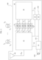
Figure 1 is a diagram exemplary of a system as per the present disclosure, -
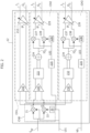
Figure 2 is a diagram exemplary of a portion of the system exemplified inFigure 1 , -
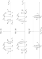
Figures 3A, 3B and 3C are diagrams exemplary of principles underlying one or more embodiments, -
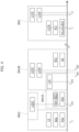
Figure 4 is a diagram exemplary of frequency bands used in possible applicative scenarios. - Corresponding numerals and symbols in the different figures generally refer to corresponding parts unless otherwise indicated.
- The figures are drawn to clearly illustrate the relevant aspects of the embodiments and are not necessarily drawn to scale.
- The edges of features drawn in the figures do not necessarily indicate the termination of the extent of the feature.
- In the ensuing description, one or more specific details are illustrated, aimed at providing an in-depth understanding of examples of embodiments of this description. The embodiments may be obtained without one or more of the specific details, or with other methods, components, materials, etc. In other cases, known structures, materials, or operations are not illustrated or described in detail so that certain aspects of embodiments will not be obscured.
- Reference to "an embodiment" or "one embodiment" in the framework of the present description is intended to indicate that a particular configuration, structure, or characteristic described in relation to the embodiment is comprised in at least one embodiment. Hence, phrases such as "in an embodiment" or "in one embodiment" that may be present in one or more points of the present description do not necessarily refer to one and the same embodiment.
- Moreover, particular conformations, structures, or characteristics may be combined in any adequate way in one or more embodiments.
- The drawings are in simplified form and are not to precise scale.
- Throughout the figures annexed herein, like parts or elements are indicated with like references/numerals unless the context indicates otherwise, and for brevity a corresponding description will not be repeated for each and every figure.
- The references used herein are provided merely for convenience and hence do not define the extent of protection or the scope of the embodiments.
- For the sake of simplicity, in the following detailed description a same reference symbol may be used to designate both a node/line in a circuit and a signal which may occur at that node or line.
- A navigation receiver operates by down converting to quasi baseband the input signal received from the satellites, which is transmitted at a plurality of radio-frequency bands, using a local oscillator to step down the input frequency and allow a baseband digital management of the satellite information.
- With reference to
Figure 1 , which diagrammatically shows a GNSS Global Navigation Satellite System) system (such as, for example, Global Positioning System (GPS), Global'naya Navigatsionnaya Sputnikovaya Sistema (GLONASS), Galileo System, or other types of satellite-based positioning systems, such global satellite positioning system comprises a constellation of a number N of satellites SC1-SCN and at least a receivingapparatus 10. - The
receiving apparatus 10 comprises an antenna RX, an analog receiving module AFE (Analog Front End), provided with a radiofrequency (RF)stage 12, and an analog-digital converter 14 (ADC), which can be implemented by hardware modules. - The
receiving apparatus 10 may be provided with a central processing unit, memories (mass memory and/or working storage) and respective interfaces (not shown in figures), comprising a microprocessor or microcontroller, for running the software resident in it. - The following embodiments are described in a non-limiting way referring to the GPS technology, however the teachings of the present disclosure can be applied also to other satellite positioning systems.
- When the
receiving apparatus 10 operates, the antenna RX receives a plurality of signals s0,...,sN from one or more satellites SC0-SCN of the constellation of satellites operating in GNSS system. For example, these signals can be modulated on at least one carrier signal having a carrier frequency FC. - For the sake of simplicity, one or more embodiments are discussed in the following with references to an exemplary case in which a signal SRF having a plurality of spectral portions in a variety of frequency bands, such an example being purely exemplary and in no way limiting.
- As exemplified in
Figure 1 , asystem 10 for receiving and processing GNSS signals in a plurality of radiofrequency (briefly, RF) bands comprises: - an antenna RX configured to receive a RF input signal SRF, e.g., a RF input signal SRF, having a spectral content in a plurality of distinct and separate frequency bands;
- a RF front-
end circuit block 12 coupled to the receiver antenna RX to receive the RF input signal SRF therefrom, the RF signal being a (e.g., frequency) modulated signal that occupies a total bandwidth of BW (in Hertz); - a local oscillator OSC configured to produce an oscillating signal OSC,
- a phase-locked loop (briefly, PLL) 11 coupled to the local oscillator OSC and comprising a voltage-controlled oscillator (briefly, VCO) coupled to the RF front-
end 12, thePLL 11 configured to provide a VCO signal VO having a further frequency FVCO and a local oscillator LO1 having a LO signal frequency that is a fraction of the VCO signal frequency Fvco, e.g., FLO1=FVCO/4. - As exemplified in
Figure 1 , thePLL 11 is configured to provide a signal which is an integer multiple of a fundamental frequency set for the GNSS standard (e.g., with f0=1.023MHz equal to the GNSS frequency, thePLL 11 may provide the VCO signal VO at a frequency about 6.285 GHz, with the local oscillator signal LO1 at a local oscillator frequency about 1571.375 MHz). - As exemplified herein, the RF front-
end 12 is configured to provide a set of processed signals I1, Q1, I2, Q2, I3, Q3. - For the sake of simplicity, one or more embodiments are discussed in the following mainly with respect to an arrangement comprising a number of three spectral portions or frequency bands in which the RF signal SRF is analyzed, such a number of frequency bands being purely exemplary and in no way limiting.
- As exemplified in
Figure 1 , the set of processed signals I1, Q1, I2, Q2, I3, Q3 comprises: - a first pair of processed signals I1, Q1 for a first frequency band of the RF signal SRF, the first pair of processed signals I1, Q1 comprising a first signal I1 and a second signal Q1 as a quadrature version of the first signal I1,
- a second pair of processed signals I2, Q2 for a second frequency band of the RF signal SRF, the second pair of processed signals I2, Q2 comprising a third signal I2 and a fourth signal Q2 as a quadrature version of the third signal I2,
- a third pair of processed signals I3, Q3 for a third frequency band of the RF signal SRF, the third pair of processed signals I3, Q3 comprising a fifth signal I3 and a sixth signal Q3 as a quadrature version of the fifth signal I3.
- As exemplified in
Figure 1 , thesystem 10 further comprises analog-to-digital converter (briefly, ADC)circuitry 14 coupled to the front-end 12 and configured to apply analog-to-digital conversion to the set of processed signals I1, Q1, I2, Q2, I3, Q3. - For instance, the
ADC circuitry 14 comprises: - a first pair of
ADC circuits ADC circuits first ADC circuit 140 configured to apply ADC processing to the first signal I1 and asecond ADC circuit 141 configured to apply ADC processing to the second signal Q1, - a second pair of
ADC circuits ADC circuits third ADC circuit 142 configured to apply ADC processing to the third signal I2 and afourth ADC circuit 144 configured to apply ADC processing to the fifth signal Q2, - a third pair of
ADC circuits fifth ADC circuit 146 configured to apply ADC processing to the fifth signal I3 and asixth ADC circuit 148 configured to apply ADC processing to the sixth signal Q3. - As exemplified in
Figure 1 , theADC circuitry 14 receives a sampling signal Fs and applies ADC conversion to the pairs of signals I1, Q1, I2, Q2, I3, Q3 via sampling such signals at a frequency of the sampling signal Fs, in a manner per se known to those of skill in the art. - For instance, the sampling signal frequency Fs may be a fraction of the frequency of the VCO signal VO, e.g., FS=VCO/6=1047.583MHz.
- For instance, after the
ADC processing 14 is applied, the ADC converted data has a frequency that is a fraction of the sampling signal frequency Fs, e.g., Fs/8=130.945MHz=128∗f0. - As exemplified in
Figure 1 , theADC circuitry 14 produces ADC converted signals S1, S2, S3, e.g., digital signals indicative of the contents in respective frequency bands of the RF signal SRF. - As exemplified in
Figure 1 , thesystem 10 further comprises: - a first (e.g., programmable) frequency divider 13 coupled to the
PLL 11 to receive the local oscillator signal LO1 therefrom, the first frequency divider 13 configured to apply frequency division (e.g., using a first programmable scaling factor K) to the local oscillator signal LO1, providing an adequate clock signal to the GNSSbase band processor 16; - a
second frequency divider 15 coupled to thePLL 11 to receive the local oscillator signal LO1 therefrom, thesecond frequency divider 15 configured to apply frequency division (e.g., using a second programmable scaling factor H) to the local oscillator signal LO1, providing a clock signal CK2 to further processing circuitry (e.g., an ARM processor); and - a
base band processor 16 coupled to theADC circuitry 14 to receive the ADC-converted signals S1, S2, S3 therefrom and coupled to the first frequency divider 13 to receive the GNSS clock CK1 therefrom, thebase band processor 16 configured to perform GNSS signal processing based on the ADC-converted signals S1, S2, S3 and on the GNSS clock CK1 in a manner per se known. - For instance, the VCO in the
PLL 11 produces a signal VO at a VCO frequency FVCO= 6144∗f0 = 6.285GHz where f0 is the fundamental GNSS frequency (e.g., f0=1.023MHz). - For instance, the local oscillator has a LO frequency FLO1 which is a fraction of the VCO frequency (e.g., FLO1=VCO/4=1536∗f0=1.5713GHz).
- For instance, the first clock CK1 has a frequency FCK1 which is a fraction of the local oscillator frequency, e.g., FCK1=FLO1/K.
- For instance, the scaling factor K of the first frequency divider 13 may have the exemplary values illustrated in Table I provided at the end of the description, which is exemplary of possible relationships between scaling factor K and local oscillator frequency, with factor of multiplication n indicating the integer multiple of the fundamental GNSS frequency.
- For instance, it may be preferable to use of signals whose frequency is a multiple of the fundamental GNSS frequency f0 so as to facilitate processing of ADC converted data and of software library development.
- For instance, the possibility to vary the clock frequency in a programmable manner facilitates current saving in case the system is used to process a subset of the incoming GNSS signals.
- As exemplified in
Figure 2 , the RFfront end 12 comprises: - a quadrature demodulator or I/Q mixer CH0 (known per se) coupled to the antenna RX (optionally, via a low-noise amplifier) to receive the RF signal SRF and coupled to the
PLL 11 to receive the local oscillator signal LO1 therefrom; the quadrature demodulator CH0 comprises a phase-shifter 20, a first "in-phase"mixer 21 and a second "quadrature"mixer 22, where thefirst mixer 21 of thequadrature demodulator second mixer 22 of the quadrature demodulator CH0 provides a second "quadrature" component Q of the (optionally, amplified) RF signal SRF by mixing the RF signal SRF with a quadrature version of the local oscillator signal LO1, that is phase-shifted by 90 degrees via phase-shifter 20; - a first signal processing channel CH1 coupled to the quadrature demodulator CH0 to receive the in-phase I and quadrature Q components of the RF signal SRF, the first signal processing channel CH1 configured to apply a first signal processing to the in-phase I and quadrature Q components of the RF signal SRF to provide the first pair of processed signals I1, Q1;
- a second signal processing channel CH2 coupled to the
quadrature demodulator PLL 11 to receive the local oscillator signal LO1 therefrom, the second signal processing channel CH2 configured to apply a second signal processing to the in-phase I and quadrature Q components of the RF signal SRF and to the local oscillator LO1 to provide the second pair of processed signals I2, Q2; and - a third signal processing channel CH3 coupled to the
quadrature demodulator PLL 11 to receive the signal VO from the voltage-controlled oscillator VCO in thePLL 11, the third signal processing channel CH3 configured to apply a third signal processing to the in-phase I and quadrature Q components of the RF signal SRF and to the VCO signal VO to provide the third pair of processed signals I3, Q3. - As appreciable to those of skill in the art, the modulated RF signal may be expressed as:

- FC is a carrier frequency of the RF signal SRF,
- ϕ is a first initial phase,
- σ is a second initial phase,
- FLO1 is a frequency of the local oscillator signal LO1,
- S(t) is the desired signal component, and
- IM(t) is the image signal component.
- As exemplified in
Figures 3A and 3B , both in case the carrier frequency Fc is greater than the local oscillator frequency FLO1 and vice versa, the desired signal component S is superimposed on the carrier frequency FC while the image signal component IM is superimposed at a frequency twice the local oscillator minus the carrier frequency (e.g., 2∗FLO1-FC). - As exemplified in
Figure 3C , after mixing the RF signal SRF in thequadrature mixer - As exemplified in
Figure 2 , each of the processing chains is configured to generate an IF signal by processing and combining intermediate signals in phase I and in quadrature Q so as to delete the contribution of the image signal I with respect to the IF signal displaced at the IF frequency as exemplified inFigure 3C . - For instance, the in-phase component I may be expressed as:


- FIF1 is the first intermediate frequency,
- ϕ is a first signal phase,
- Θ is a second signal phase.
- As exemplified in
Figure 2 , the first signal processing chain CH1 comprises: - a
first buffer 210 having a first buffer input node coupled to thefirst mixer 21 to receive the in-phase component I and a second buffer input node coupled to thesecond mixer 22 to receive the quadrature component Q, thefirst buffer 210 configured to provide a first IF signal IF1 based on the I and Q components provided by thequadrature demodulator - a first variable gain amplifier (briefly, VGA) 212 coupled to the
first buffer 210 to receive the first IF signal IF1 and to applyvariable gain amplification 212 thereto (and, optionally, also anti-alias filtering), providing the first processed signal I1 and the second processed signal Q1 of the first pair of processed signals I1, Q1. - As exemplified in
Figure 2 , the second signal processing chain CH2 comprises: - a
second buffer 220 having a first buffer input node coupled to thefirst mixer 21 to receive the in-phase component I and a second buffer input node coupled to thesecond mixer 22 to receive the quadrature component Q; - a
filtering stage 222, such as a polyphase filter (e.g., a Hartley or Weaver filter, known per se), configured to apply signal filtering to the I and Q components provided by thequadrature demodulator filtering stage 222 may be tuned to remove the image signal of GNSS signals in a first frequency band selected out of L5, E5a and B2a frequency bands; - an
adder stage 224 configured to combine therebetween the filtered I/Q components, providing a second IF signal IQ2 as a superposition of the filtered I/Q components; - a
LO frequency divider 225 coupled to thePLL 11 to receive the local oscillator signal LO1 therefrom, theLO frequency divider 225 being configured to apply frequency division (e.g., via a programmable scaling factor M) to the local oscillator signal LO1, providing a second LO signal LO2 having a second LO frequency FLO2 that is a fraction of the local oscillator frequency FLO1 (e.g., FLO2=FLO1/M); - a
second quadrature demodulator shifter 228, a second "in-phase"mixer 226 and a second "quadrature"mixer 227, where the second in-phase mixer 226 of thesecond quadrature demodulator second quadrature mixer 226 of thequadrature demodulator shifter 226; and - a
second VGA 229 coupled to thesecond quadrature mixer second quadrature demodulator second VGA 229 configured to provide the third I2 and fourth Q2 processed signals. - For instance, document Fayrouz. Haddad, Lakhdar Zaid, Wenceslas Rahajandraibe, Oussama Frioui: "Polyphase Filter Design Methodology for Wireless Communication Applications", Salma Ait Fares, Mobile and Wireless Communications, Network layer and circuit level design, IntechOpen, pp.219-246, 2010, doi: 10.5772/7707 hal-01895400 discusses a
filter stage 222 suitable for use in one or more embodiments. - For instance, the signal IQ2 comprises the signal at the first intermediate frequency FIF1 cleaned from the image signal and may be expressed as:

FLO1 is the frequency of the local oscillator signal LO1. - As exemplified in
Figure 2 , the off-loop frequency divider 235 is used to bring the signal components I, Q at the first intermediate frequency IF1 down to a further reduced intermediate frequency IF2, e.g., with IF2=IF1-LO2. This may facilitate further signal processing by the subsequent A/D converter circuitry 14, for instance. - For instance, an in-phase signal IIF2 and a quadrature signal QIF2 produced by the second down-
conversion stage 

FIF2 is the second intermediate frequency, e.g., FIF2=|FIF1|-|FLO2|. - As exemplified in
Figure 2 , the third signal processing chain CH3 comprises: - a
third buffer 230 having a first buffer input node coupled to the first in-phase mixer 21 to receive the in-phase component I and a second buffer input node coupled to thesecond mixer 22 to receive the quadrature component Q; - a
third filtering stage 232, such as a polyphase filter as in the case of thesecond filtering stage 222 but tuned to work in a different frequency (e.g., for GNSS signals in a second frequency band selected out of L2 and BW3 frequency bands), configured to apply signal filtering to the I and Q components provided by thequadrature demodulator - a
further adder stage 234 configured to combine therebetween the filtered I/Q components, providing a third IF signal IQ3 as a superposition of the filtered I/Q components; - a
VCO frequency divider 235 coupled to thePLL 11 to receive the VCO signal VO therefrom, theVCO frequency divider 235 being configured to apply frequency division (e.g., via a programmable scaling factor G) to the VCO signal VO, providing a third LO signal LO3 having a third frequency FLO3 that is a fraction of the VCO frequency FLO3 (e.g., FLO3=FLO2/G); - a
third quadrature demodulator shifter 238, a third "in-phase"mixer 236 and a third "quadrature"mixer 238, where the third in-phase mixer 236 of thethird quadrature demodulator third quadrature mixer 236 of thequadrature demodulator shifter 236; and - a
third VGA 239 coupled to thethird quadrature mixer third quadrature demodulator third VGA 239 configured to provide the fifth I3 and sixth Q3 processed signals. - As exemplified herein, the
third filtering stage 232 is configured to filter the image signal from the second IF signal at the second intermediate frequency signal IF2, producing the signal IQ3 as a result. - For instance, the
VCO frequency divider 235 uses a scaling factor G about 18 or 20, providing the third LO signal LO3 with a third LO frequency FLO3 which is a fraction G of the frequency of VCO, e.g., FLO3=FVCO/G=FVCO/18 or FVCO/20. - It is noted that the
phase shifters Figure 2 are purely exemplary an in no way mandatory, as in one or more embodiments the signals LO1, LO2, LO3 can be provided (e.g., by respective divider blocks) as a pair of phase-shifted signals in quadrature therebetween. - As exemplified in
Figure 2 , the scaling factor G of theVCO divider 235 is an even integer number so as to provide the local oscillator to thethird quadrature mixer - For instance, the presence of the
VCO divider 235 facilitates obtaining signals I3, Q3 which have a lower intermediate frequency FIF3 with respect to the signals I, Q provided by thefirst quadrature mixer D converter circuitry 14, for instance. - As exemplified herein, a
system 12 comprises: - an input node SRF configured to receive a set of global navigation satellite system, GNSS signals S0, SN transmitted from a plurality of GNSS satellites SC0, SCN over a set of carrier frequencies f1, f11, f2, f3A1, f3A2, f3B1, f3B2, Fc;
- a phase-locked loop,
PLL 11 configured to provide a first local oscillator signal LO1 and a voltage-controlled oscillator, VCO signal VO; - a first quadrature demodulator CH0 coupled to the input node and to the PLL, the first quadrature demodulator CH0 configured to apply
quadrature demodulation processing - For instance, in-phase signals of the first set of in-phase signals and quadrature signals of the first set of quadrature signals have a first intermediate frequency FIF1 lower than carrier frequencies of the set of carrier frequencies of GNSS signals of the set of GNSS signals.
- As exemplified herein, the system further comprises:
- a first signal processing chain CH1 coupled to the first quadrature demodulator to receive the set of in-phase signals and the set of quadrature signals, the first signal processing chain comprising a first variable gain amplifier,
VGA 212 coupled to the first quadrature demodulator, the VGA configured to apply a first variable gain amplification to the first set of in-phase signals and to the first set of quadrature signals, providing a first in-phase signal component I1 and a first quadrature signal component Q1 as a result; - a second signal processing chain CH2 coupled to the first quadrature demodulator to receive the first set of in-phase signals and the first set of quadrature signals and coupled to the PLL to receive the first local oscillator signal, the second signal processing chain comprising:
- a first
polyphase filter 222 configured to apply polyphase filtering to the first set of in-phase signals and to the first set of quadrature signals, producing a first set of filtered in-phase signals and a first set of filtered quadrature signals as a result; - a
first adder 224 coupled to the first polyphase filter to receive the first set of filtered in-phase signals and the first set of filtered quadrature signals, the first adder configured to provide a first sum signal IQ2 as a sum of the first set of filtered in-phase signals and the first set of filtered quadrature signals, - a
first frequency divider 225 configured to apply frequency division to the first local oscillator signal, producing a second local oscillator signal LO2 as a result, wherein the second local oscillator signal has a second local oscillator frequency that is a fraction of the frequency of the local oscillator signal; - a
second quadrature demodulator second quadrature demodulator - a
second VGA 229 configured to apply a second variable gain amplification to the second set of in-phase signals and to the second set of quadrature signals, the second VGA configured to produce a second in-phase signal component I2 and a second quadrature signal component Q2 as a result;
- a first
- a third signal processing chain CH3 coupled to the first quadrature demodulator to receive the set of in-phase signals and the set of quadrature signals and coupled to the PLL to receive the VCO signal, the third signal processing chain comprising:
- a second
polyphase filter 232 configured to apply second polyphase filtering to the first set of in-phase signals and to the first set of quadrature signals, producing a second set of filtered in-phase signals and a second set of filtered quadrature signals as a result; - a
second adder 234 coupled to the second polyphase filter to receive the second set of filtered in-phase signals and the second set of filtered quadrature signals therefrom, the second adder configured to provide a second sum signal IQ3 as a sum of the second set of filtered in-phase signals and the second set of filtered quadrature signals; - a
second frequency divider 235 configured to apply a second frequency division to the VCO signal, producing a third local oscillator signal LO3 as a result, wherein the third local oscillator signal has a third local oscillator frequency that is a fraction of the frequency of the VCO signal; - a
third quadrature demodulator third quadrature demodulator - a
third VGA 239 configured to apply a third variable gain amplification to the third set of in-phase signals and to the third set of quadrature signals, the third VGA configured to produce a third in-phase signal component I3 and a third quadrature signal component Q3 as a result.
- a second
- As exemplified herein, the first local oscillator signal has a first local oscillator frequency that is fraction of the frequency of the VCO signal.
- As exemplified herein, the first frequency divider is configured to apply frequency division using a first programmable frequency division factor.
- As exemplified herein, the second frequency divider is configured to apply frequency division using a second programmable frequency division factor, preferably programmable in a range 18 to 20.
- As exemplified herein, GNSS signals of the set of GNSS signals transmitted from a plurality of GNSS satellites over a set of carrier frequencies comprise signals transmitted over frequency bands distinct and separate BW1, BW2, BW3A, BW3B.
- As exemplified herein, GNSS signals of the set of GNSS signals transmitted from a plurality of GNSS satellites over the set of carrier frequencies comprise at least two of:
- a first GNSS signal S0 transmitted over a first carrier frequency f1, f11,
- a second GNSS signal SN transmitted over a second carrier frequency f2, the second carrier frequency higher than the first carrier frequency,
- a third GNSS signal SRF transmitted over a third carrier frequency f3A1, f3A2, f3B1, f3B2 higher than the second carrier frequency.
- As exemplified herein, the first set of in-phase signals and the first set of quadrature signals comprise at least one image signal component, and the first polyphase filter is configured to filter at least one image signal component of the first set of in-phase signals and of the first set of quadrature signals, producing the first set of filtered in-phase signals and the first set of filtered quadrature signals exempt from at least one image signal component as a result.
- As exemplified herein, the first set of in-phase signals and the first set of quadrature signals comprise at least one image signal component and the second polyphase filter is configured to filter at least one image signal component of the first set of in-phase signals and the first set of quadrature signals, producing the second set of filtered in-phase signals and the second set of filtered quadrature signals exempt from at least one image signal component as a result.
- As exemplified herein, a (e.g., RF)
receiver 100 comprises: - a
system 12 as per the present disclosure, - an antenna RX configured to receive the set of GNSS signals and coupled to the to the input node of the system to provide the received set of GNSS signals thereto,
- a set of analogue-to-digital converter, ADC,
circuits 14 coupled to the first signal processing chain, the second signal processing chain and to the third signal processing chain, the set of ADC circuits configured to apply analogue-to-digital conversion to the first in-phase component, the first quadrature component, the second in-phase component, the second quadrature component, the third in-phase component and the third quadrature component, providing a set of digital signal components as a result. - As exemplified herein, the receiver comprises a
baseband circuit block 16 coupled to the set ofADC circuits 14, the base stand circuit block configured to apply baseband signal processing to the set of digital signals received from the set of ADC converters. - As exemplified herein, the set of ADC converter circuits is configured to apply the analog-to-digital conversion based on a sampling signal Fs having a sampling frequency that is a multiple of a fundamental GNSS frequency.
- As exemplified in
Figure 4 , the system exemplified inFigures 1 and2 can be used to process signals which have a carrier frequency band FC that may fall in a variety of frequency bands such as, for instance: - a first frequency band BW1 comprising signals that fall in a first frequency range f1-f11, e.g., between 1559 MHz and 1606 MHz;
- a second frequency band BW2, e.g., centered around a second frequency band f2, such as a frequency about 1176 MHz;
- a third frequency band BW3A in a third frequency range, e.g., f3A1-f3A2 between 1200 MHz and 1250 MHz, such as 1207.14 MHz, for instance;
- a fourth frequency band BW3B in a fourth frequency range f3B1-f3B2, such as between 1258 MHz and 1289 MHz, for instance.
- For instance, GNSS signals S0,...,SN may be transmitted and received from satellites in a variety of known GNSS constellations using any of these frequency bands BW1, BW2, BW3A, BW4A.
- For instance, the first signal processing chain CH1 may be suitable to process a RF signal received in the first frequency band BW1, e.g., from a first set of GNSS constellation of satellites L1CA, E1, L1C, B1C, B1I, LOF1, L1OC and/or any other signal in these frequency bands.
- For instance, the second signal processing chain CH2 may be suitable to process a RF signal received in the second frequency band BW2, e.g., from a second set of constellations L5, B2a, E5a.
- For instance, the third signal processing chain CH3 may be suitable to process a RF signal SRF received in the third frequency band BW3A (e.g., from a third set of constellations L2C, B2b, B2l, E5b, L3OC) or in the fourth frequency band BW3B (e.g., from a fourth set of constellations L2OC, L2OF, B3l, E6).
- Table II provided at the end of the description exemplifies settings of the first signal processing chain CH1, such as carrier frequency Fc, bandwidth BW, VCO signal frequency FVCO, first local oscillator signal frequency FLO1 and intermediate frequency IF1 which may be used to process signals from a variety of constellations configured to transmit signals over frequency bands (e.g., L1c/a, L1C, E1, B1I, B1C, LOF1) in the first bandwidth BW1.
- Table III provided at the end of the description exemplifies settings of the second signal processing chain CH2, such as carrier frequency Fc, bandwidth BW, VCO signal frequency FVCO, first local oscillator signal frequency FLO1, second LO signal frequency FLO2, scaling factor M, intermediate frequency IF2 and maximum frequency Max F which may be used to process signals from a variety of the constellations configured to transmit signals over frequency bands (e.g., L5, such as GPS and others, B2a, E5a) in the second bandwidth BW2.
- Table IV provided at the end of the description exemplifies settings of the third signal processing chain CH3, such as carrier frequency Fc, bandwidth BW, VCO signal frequency FVCO, first local oscillator signal frequency FLO1, third local oscillator signal frequency FLO3, scaling factor G, third intermediate frequency IF3 and maximum frequency Max F which may be used to process signals from a variety of constellations configured to transmit over frequency bands (e.g., L2C, B2b, B2l, E5b) in the third bandwidth BW3A.
- Table V provided at the end of the description exemplifies of the third signal processing chain CH3 such as carrier frequency FC, bandwidth BW, VCO signal frequency FVCO, first local oscillator signal frequency FLO1, third local oscillator signal frequency FLO3, scaling factor G, third intermediate frequency IF3 and maximum frequency Max F which may be used to process signals from a variety of constellations configured to transmit over frequency bands (e.g., alternative constellations L2OC, L2OF, B3l, E6) in the fourth bandwidth BW3B.
- Table VI provided at the end of the description is exemplary of combinations of constellations and respective names of channels that may be used to process signals received from such exemplary combinations of constellations.
- As exemplified in Table VI, the system as exemplified in
Figures 1 and2 provides flexibility to deal with a wide variety of application scenarios, as those listed in the Table VI are purely exemplary an in no way limiting. - It will be otherwise understood that the various individual implementing options exemplified throughout the figures accompanying this description are not necessarily intended to be adopted in the same combinations exemplified in the figures. One or more embodiments may thus adopt these (otherwise non-mandatory) options individually and/or in different combinations with respect to the combination exemplified in the accompanying figures.
- Without prejudice to the underlying principles, the details and embodiments may vary, even significantly, with respect to what has been described by way of example only, without departing from the extent of protection. The extent of protection is defined by the annexed claims.
TABLE I K LO1 / K 2^n * f0 6 256∗f0 n = 8 12 128∗f0 n = 7 24 64∗f0 n = 6 48 32∗f0 n = 5 96 16∗f0 n = 4 TABLE II Constell. frequency band FC [MHz] BW [MHz] FVCO [MHz] FLO1 [MHz] IF1 [MHz] Max F [MHz] L1C/A or L1C 1575.42 2.046 6285.5 1571.375 4.045 5.068 E1 1575.42 4.092 6285.5 1571.375 4.045 6.091 B1I 1561.098 4.092 6285.5 1571.375 -10.277 12.323 B1C 1575.42 32.736 6285.5 1571.375 4.045 20.413 LOF1 1602 7.875 6285.5 1571.375 30.625 34.5625 TABLE III Constell. name or frequency band FC [MHz] BW [MHz] FVCO [MHz] FLO1 [MHz] IF1 [MHz] M FLO2 [MHz] IF2 [MHz] Max F [MHz] GPS - L5 1176.45 20.46 6285.5 1571.375 394.925 4 392.8438 2.08125 12.31125 E5A 1176.45 20.46 6285.5 1571.375 394.925 4 392.8438 2.08125 12.31125 B2A 1176.45 20.46 6285.5 1571.375 394.925 4 392.8438 2.08125 12.31125 IRNSS - L5 1176.45 2.046 6285.5 1571.375 394.925 4 392.8438 2.08125 3.10425 TABLE IV Constell. frequency band FC [MHz] BW [MHz] FVCO [MHz] FLO1 [MHz] IF1 [MHz] G FLO3 [MHz] IF3 [MHz] Max F [MHz] L2C 1227.6 1.023 6285.5 1571.375 343.775 18 349.1944 5.419444 5.930944 E5b 1207.14 20.46 6285.5 1571.375 364.235 18 349.1944 -15.0406 25.27056 B21 1207.14 6285.5 1571.375 364.235 18 349.1944 -15.0406 B2B 1207.14 20.46 6285.5 1571.375 364.235 18 349.1944 -15.0406 25.27056 LOF2 1246 6.125 6285.5 1571.375 325.375 18 349.1944 23.81944 26.88194 L2CC 1248.06 2.046 6285.5 1571.375 323.315 18 349.1944 25.87944 26.90244 L3CC 1202.025 2.046 6285.5 1571.375 369.35 18 349.1944 -20.1556 21.17856 TABLE V Constell. frequency band FC [MHz] BW [MHz] FVCO [MHz] FLO1 [MHz] IF1 [MHz] G FLO3 [MHz] IF3 [MHz] Max F [MHz] L2C 1227.6 1.023 6285.5 1571.375 343.775 20 314.275 -29.5 30.0115 E6I 1278.75 10.23 6285.5 1571.375 292.625 20 314.275 21.65 26.765 B3I 1268.52 20.46 6285.5 1571.375 302.855 20 314.275 11.42 21.65 TABLE VI L1C/A L2C LOF1 LOF2 E1 E5b B1I B2I CH1, CH3 1575.42 1227.6 1602 1246 1575.42 1207.14 1561.09 1207.14 L1C/A or L1C L2C LOF1 LOF2 E1 E5b B11 B1C 621 B2B CH1, CH3 1575.42 1575.42 1227.6 1602 1246 1575.42 1207.14 1561.09 1575.42 1207.14 1207.14 L1C/A L5 E1 E5A B1I B2A L5 CH1, CH2 1575.42 1176.45 1575.42 1176.45 1561.09 1176.45 1176.45 L1C/A or L1C L5 E1 E5A B11 or B1C B2A L5 CH1, CH3 1575.42 1575.42 1176.45 1575.42 1176.45 1561.09 1575.42 1176.45 1176.45 L1C/A or L1C L2C E1 E61 B11 or B1C B3I CH1, CH3 1575.42 1575.42 1227.6 1575.42 1278.75 1561.09 1575.42 1268.52 L1C/A L2C L5 E1 E5B E5A B1I B21 B2A CH1, CH2, CH3 1575.45 1227.6 1176.45 1575.42 1207.14 1176.45 1561.09 1207.14 1176.45 L1C/A or L1C L2C L5 E1 E5B E5A B11 or B1C B2I or B2B B2A CH1, CH2, CH3 1575.42 1575.42 1227.6 1176.45 1575.42 1207.14 1176.45 1561.09 1575.42 1207.14 1207.14 1176.45 L1C/A or L1C L2C L5 E1 E61 E5A B11 or B1C B3I B2A CH1, CH2, CH3 1575.42 1575.42 1227.6 1176.45 1575.42 1278.75 1176.45 1561.09 1575.42 1268.52 1176.45 L1C L2C L5 L1OC L2OC L3CC CH1, CH2, CH3 1575.42 1227.6 1176.45 1600.99 1248.06 1202.02
Claims (11)
- A system (10), comprising:an input node (SRF) configured to receive a set of global navigation satellite system, GNSS signals (S0, SN) transmitted from a plurality of GNSS satellites (SC0, SCN) over a set of carrier frequencies (f1, f11, f2, f3A1, f3A2, f3B1, f3B2, Fc);a phase-locked loop, PLL (11) configured to provide a first local oscillator signal (LO1) and a voltage-controlled oscillator, VCO signal (VO);a first quadrature demodulator (CH0) coupled to the input node (SRF) and to the PLL (11), the first quadrature demodulator (CH0) configured to apply quadrature demodulation processing (20, 21, 22) to the set of GNSS signals (S0, SN) based on the local oscillator signal (LO1) received from the PLL (11), the first quadrature demodulator (CH0) providing a first set of in-phase signals (I) and a first set of quadrature signals (Q) as a result,wherein in-phase signals of the first set of in-phase signals (I) and quadrature signals of the first set of quadrature signals (Q) have a first intermediate frequency (FIF1) lower than carrier frequencies of the set of carrier frequencies (f1, f11, f2, f3A1, f3A2, f3B1, f3B2, FC) of GNSS signals of the set of GNSS signals (S0, SN),a first signal processing chain (CH1) coupled to the first quadrature demodulator (CH0) to receive the set of in-phase signals (I) and the set of quadrature signals (Q), the first signal processing chain (CH1) comprising a first variable gain amplifier, VGA (212) coupled to the first quadrature demodulator (CH0), the VGA (212) configured to apply a first variable gain amplification to the first set of in-phase signals (I) and to the first set of quadrature signals (Q), providing a first in-phase signal component (I1) and a first quadrature signal component (Q1) as a result;a second signal processing chain (CH2) coupled to the first quadrature demodulator (CH0) to receive the first set of in-phase signals (I) and the first set of quadrature signals (Q) and coupled to the PLL (11) to receive the first local oscillator signal (LO1), the second signal processing chain (CH2) comprising:a first polyphase filter (222) configured to apply polyphase filtering to the first set of in-phase signals (I) and to the first set of quadrature signals (Q), producing a first set of filtered in-phase signals and a first set of filtered quadrature signals as a result;a first adder (224) coupled to the first polyphase filter (222) to receive the first set of filtered in-phase signals and the first set of filtered quadrature signals, the first adder (224) configured to provide a first sum signal (IQ2) as a sum of the first set of filtered in-phase signals and the first set of filtered quadrature signals,a first frequency divider (225) configured to apply frequency division to the first local oscillator signal (LO1), producing a second local oscillator signal (LO2) as a result, wherein the second local oscillator signal (LO2) has a second local oscillator frequency that is a fraction of the frequency of the local oscillator signal (LO1);a second quadrature demodulator (226, 227, 228) coupled to the first adder (224) and to the first frequency divider (225), the second quadrature demodulator (226, 227, 228) configured to apply second quadrature demodulation processing to the first sum signal (IQ2), providing, based on the second local oscillator signal (LO2), a second set of in-phase signals and a second set of quadrature signals, the second set of in-phase signals and the second set of quadrature signals having a second intermediate frequency (IF2) lower than the first intermediate frequency (IF1, FIF1), anda second VGA (229) configured to apply a second variable gain amplification to the second set of in-phase signals and to the second set of quadrature signals, the second VGA (229) configured to produce a second in-phase signal component (I2) and a second quadrature signal component (Q2) as a result;a third signal processing chain (CH3) coupled to the first quadrature demodulator (CH0) to receive the set of in-phase signals (I) and the set of quadrature signals (Q) and coupled to the PLL (11) to receive the VCO signal (VO), the third signal processing chain (CH3) comprising:a second polyphase filter (232) configured to apply second polyphase filtering to the first set of in-phase signals (I) and to the first set of quadrature signals (Q), producing a second set of filtered in-phase signals and a second set of filtered quadrature signals as a result;a second adder (234) coupled to the second polyphase filter (232) to receive the second set of filtered in-phase signals and the second set of filtered quadrature signals therefrom, the second adder (234) configured to provide a second sum signal (IQ3) as a sum of the second set of filtered in-phase signals and the second set of filtered quadrature signals;a second frequency divider (235) configured to apply a second frequency division to the VCO signal (VO), producing a third local oscillator signal (LO3) as a result, wherein the third local oscillator signal (LO3) has a third local oscillator frequency that is a fraction of the frequency of the VCO signal (VO);a third quadrature demodulator (236, 237, 238) coupled to the second adder (234) and to the second frequency divider (235), the third quadrature demodulator (236, 237, 238) configured to apply third quadrature demodulation processing to the second sum signal (IQ3), providing, based on the third local oscillator signal (LO3), a third set of in-phase signals and a third set of quadrature signals, the third set of in-phase signals and the third set of quadrature signals having a third intermediate frequency (IF3) lower than the second intermediate frequency (IF2), anda third VGA (239) configured to apply a third variable gain amplification to the third set of in-phase signals and to the third set of quadrature signals, the third VGA (239) configured to produce a third in-phase signal component (I3) and a third quadrature signal component (Q3) as a result.
- The system (10) according to claim 1, wherein the first local oscillator signal (LO1) has a first local oscillator frequency that is fraction of the frequency of the VCO signal (VO).
- The system (10) according to claim 1 or claim 2, wherein the first frequency divider (225) is configured to apply frequency division using a first programmable frequency division factor.
- The system according to any of the previous claims, wherein the second frequency divider (235) is configured to apply frequency division using a second programmable frequency division factor, preferably programmable in a range 18 to 20.
- The system (10) according to any of the previous claims, wherein GNSS signals of the set of GNSS signals (S0, SN) transmitted from a plurality of GNSS satellites (SC0, SCN) over a set of carrier frequencies (f1, f11, f2, f3A1, f3A2, f3B1, f3B2, FC) comprise signals transmitted over frequency bands distinct and separate (BW1, BW2, BW3A, BW3B).
- The system (10) according to any of the previous claims, wherein GNSS signals of the set of GNSS signals (S0, SN) transmitted from a plurality of GNSS satellites (SC0, SCN) over the set of carrier frequencies (f1, f11, f2, f3A1, f3A2, f3B1, f3B2, FC) comprise at least two of:a first GNSS signal (S0) transmitted over a first carrier frequency (f1, f11),a second GNSS signal (SN) transmitted over a second carrier frequency (f2), the second carrier frequency (f2) higher than the first carrier frequency,a third GNSS signal (SRF) transmitted over a third carrier frequency (f3A1, f3A2, f3B1, f3B2) higher than the second carrier frequency (f2).
- The system (10) according to any of the previous claims, wherein:the first set of in-phase signals (I) and the first set of quadrature signals (Q) comprise at least one image signal component, andthe first polyphase filter (222) is configured to filter the at least one image signal component of the first set of in-phase signals (I) and of the first set of quadrature signals (Q), producing the first set of filtered in-phase signals and the first set of filtered quadrature signals exempt from at least one image signal component as a result.
- The system (10) according to any of the previous claims, wherein:the first set of in-phase signals (I) and the first set of quadrature signals (Q) comprise at least one image signal component, andthe second polyphase filter (232) is configured to filter at least one image signal component of the first set of in-phase signals (I) and the first set of quadrature signals (Q), producing the second set of filtered in-phase signals and the second set of filtered quadrature signals exempt from at least one image signal component as a result.
- A receiver (100), comprising:a system (10) according to any of the previous claims,an antenna (RX) configured to receive the set of GNSS signals (S0, SN) and coupled to the to the input node (SRF) of the system (10) to provide the received set of GNSS signals thereto,a set of analogue-to-digital converter, ADC, circuits (14), coupled to the first signal processing chain (CH1), the second signal processing chain (CH2) and to the third signal processing chain (CH3), the set of ADC circuits (14) configured to apply analogue-to-digital conversion to the first in-phase component (I1), the first quadrature component (Q1), the second in-phase component (I2), the second quadrature component (Q2), the third in-phase component (I3) and the third quadrature component (Q3), providing a set of digital signal components as a result.
- The receiver (100) according to claim 9, comprising a baseband circuit block (16) coupled to the set of ADC circuits (14), the base stand circuit block (16) configured to apply baseband signal processing to the set of digital signals received from the set of ADC converters (14).
- The receiver (100) according to claim 9 or claim 10, wherein the set of ADC converter circuits (14) is configured to apply the analog-to-digital conversion based on a sampling signal (FS) having a sampling frequency that is a multiple of a fundamental GNSS frequency.
Applications Claiming Priority (1)
| Application Number | Priority Date | Filing Date | Title |
|---|---|---|---|
| IT102022000011330A IT202200011330A1 (en) | 2022-05-30 | 2022-05-30 | SYSTEM AND RECEIVER FOR GNSS SIGNALS |
Publications (2)
| Publication Number | Publication Date |
|---|---|
| EP4286896A1 true EP4286896A1 (en) | 2023-12-06 |
| EP4286896B1 EP4286896B1 (en) | 2024-12-11 |
Family
ID=82694183
Family Applications (1)
| Application Number | Title | Priority Date | Filing Date |
|---|---|---|---|
| EP23173209.0A Active EP4286896B1 (en) | 2022-05-30 | 2023-05-12 | System and receiver for gnss signals |
Country Status (4)
| Country | Link |
|---|---|
| US (1) | US12216213B2 (en) |
| EP (1) | EP4286896B1 (en) |
| CN (1) | CN117148395A (en) |
| IT (1) | IT202200011330A1 (en) |
Citations (3)
| Publication number | Priority date | Publication date | Assignee | Title |
|---|---|---|---|---|
| US20060176215A1 (en) * | 2005-02-10 | 2006-08-10 | Dubash Noshir B | Reconfigurable downconverter for a multi-band positioning receiver |
| US20120026039A1 (en) * | 2010-07-27 | 2012-02-02 | Texas Instruments Incorporated | Single rf receiver chain architecture for gps, galileo and glonass navigation systems, and other circuits, systems and processes |
| CN210351144U (en) * | 2019-11-22 | 2020-04-17 | 成都旋极星源信息技术有限公司 | Multimode multiband three-channel radio frequency receiver |
Family Cites Families (5)
| Publication number | Priority date | Publication date | Assignee | Title |
|---|---|---|---|---|
| JP2002368642A (en) * | 2001-06-08 | 2002-12-20 | Sony Corp | Receiver and IC |
| DE602005018492D1 (en) * | 2005-11-03 | 2010-02-04 | Qualcomm Inc | Multi-band receiver for signals from navigation satellites (GNSS) |
| DE102008026698A1 (en) * | 2008-06-04 | 2009-12-17 | Fraunhofer-Gesellschaft zur Förderung der angewandten Forschung e.V. | Multi-frequency band receiver |
| US20130187810A1 (en) * | 2011-10-28 | 2013-07-25 | Maxime Leclercq | Method And System For An Embedded And Hosted Architecture For A Medium Earth Orbit Satellite And Low Earth Orbit Satellite Positioning Engine |
| EP3648517A4 (en) * | 2017-06-30 | 2020-07-08 | Sony Semiconductor Solutions Corporation | Wireless terminal, information processing device, information processing method, and program |
-
2022
- 2022-05-30 IT IT102022000011330A patent/IT202200011330A1/en unknown
-
2023
- 2023-05-04 US US18/312,157 patent/US12216213B2/en active Active
- 2023-05-12 EP EP23173209.0A patent/EP4286896B1/en active Active
- 2023-05-29 CN CN202310616854.1A patent/CN117148395A/en active Pending
Patent Citations (3)
| Publication number | Priority date | Publication date | Assignee | Title |
|---|---|---|---|---|
| US20060176215A1 (en) * | 2005-02-10 | 2006-08-10 | Dubash Noshir B | Reconfigurable downconverter for a multi-band positioning receiver |
| US20120026039A1 (en) * | 2010-07-27 | 2012-02-02 | Texas Instruments Incorporated | Single rf receiver chain architecture for gps, galileo and glonass navigation systems, and other circuits, systems and processes |
| CN210351144U (en) * | 2019-11-22 | 2020-04-17 | 成都旋极星源信息技术有限公司 | Multimode multiband three-channel radio frequency receiver |
Non-Patent Citations (1)
| Title |
|---|
| FAYROUZ. HADDADLAKHDAR ZAIDWENCESLAS RAHAJANDRAIBEOUSSAMA FRIOUI: "Polyphase Filter Design Methodology for Wireless Communication Applications", SALMA AIT FARES, MOBILE AND WIRELESS COMMUNICATIONS, NETWORK LAYER AND CIRCUIT LEVEL DESIGN, INTECHOPEN, 2010, pages 219 - 246 |
Also Published As
| Publication number | Publication date |
|---|---|
| US12216213B2 (en) | 2025-02-04 |
| EP4286896B1 (en) | 2024-12-11 |
| IT202200011330A1 (en) | 2023-11-30 |
| CN117148395A (en) | 2023-12-01 |
| US20230384459A1 (en) | 2023-11-30 |
Similar Documents
| Publication | Publication Date | Title |
|---|---|---|
| US9482760B2 (en) | Receiver for simultaneous reception of signals from multiple GNSS satellite systems | |
| US8604974B2 (en) | Glonass/GPS de-rotation and filtering with ADC sampling at 60-80 MSPS | |
| EP1671417B1 (en) | Receiver including an oscillation circuit for generating an image rejection calibration tone | |
| US8306154B2 (en) | Multi-frequency band receiver | |
| US10101461B2 (en) | Radio frequency circuit structure for implementing function of converting GNSS satellite signal into baseband signal | |
| US6856794B1 (en) | Monolithic GPS RF front end integrated circuit | |
| WO2008144990A1 (en) | A general configurable rf processing method and system for navigation satellite signal | |
| CN101174840B (en) | Programmable direct radio frequency digitization receiver with multiple groups of frequency bands and method thereof | |
| CN104237910A (en) | Multi-channel navigation radio frequency receiver | |
| CN102243308A (en) | Single-channel radiofrequency receiver and frequency planning method thereof | |
| CN107942355A (en) | A kind of parallel GNSS radio-frequency transmitters of four mould triple channels | |
| CN202182942U (en) | Global navigation system double-channel radio frequency receiver with low power consumption | |
| US7047023B1 (en) | GPS RF front end IC with frequency plan for improved integrability | |
| CN113037307B (en) | Satellite receiver chip and satellite receiver system | |
| US9791574B2 (en) | Method and system for repurposing of a global navigation satellite system receiver for receiving low-earth orbit communication satellite signals | |
| CN110244327A (en) | A satellite positioning receiver and its radio frequency front end | |
| EP4286896B1 (en) | System and receiver for gnss signals | |
| US20160025861A1 (en) | Method and system for indoor global navigation satellite system detection utilizing low-earth orbit satellite signals | |
| CN111988050B (en) | SOC chip sampling rate selection method and device based on radio frequency direct sampling | |
| RU2097919C1 (en) | Microwave receiver of signals from satellite navigation systems | |
| RU2124214C1 (en) | Device which receives signals from satellite navigation systems | |
| CN118348575B (en) | RF receiver, positioning chip and positioning system | |
| US7616705B1 (en) | Monolithic GPS RF front end integrated circuit | |
| RU2110149C1 (en) | Receiver for signals of satellite navigation systems | |
| CN110196437B (en) | Satellite signal receiving circuit and satellite signal receiving method |
Legal Events
| Date | Code | Title | Description |
|---|---|---|---|
| PUAI | Public reference made under article 153(3) epc to a published international application that has entered the european phase |
Free format text: ORIGINAL CODE: 0009012 |
|
| STAA | Information on the status of an ep patent application or granted ep patent |
Free format text: STATUS: THE APPLICATION HAS BEEN PUBLISHED |
|
| AK | Designated contracting states |
Kind code of ref document: A1 Designated state(s): AL AT BE BG CH CY CZ DE DK EE ES FI FR GB GR HR HU IE IS IT LI LT LU LV MC ME MK MT NL NO PL PT RO RS SE SI SK SM TR |
|
| STAA | Information on the status of an ep patent application or granted ep patent |
Free format text: STATUS: REQUEST FOR EXAMINATION WAS MADE |
|
| 17P | Request for examination filed |
Effective date: 20240429 |
|
| RBV | Designated contracting states (corrected) |
Designated state(s): AL AT BE BG CH CY CZ DE DK EE ES FI FR GB GR HR HU IE IS IT LI LT LU LV MC ME MK MT NL NO PL PT RO RS SE SI SK SM TR |
|
| GRAP | Despatch of communication of intention to grant a patent |
Free format text: ORIGINAL CODE: EPIDOSNIGR1 |
|
| STAA | Information on the status of an ep patent application or granted ep patent |
Free format text: STATUS: GRANT OF PATENT IS INTENDED |
|
| RIC1 | Information provided on ipc code assigned before grant |
Ipc: G01S 19/37 20100101ALI20240712BHEP Ipc: G01S 19/35 20100101ALI20240712BHEP Ipc: G01S 19/32 20100101ALI20240712BHEP Ipc: G01S 19/33 20100101ALI20240712BHEP Ipc: G01S 19/29 20100101AFI20240712BHEP |
|
| INTG | Intention to grant announced |
Effective date: 20240806 |
|
| GRAS | Grant fee paid |
Free format text: ORIGINAL CODE: EPIDOSNIGR3 |
|
| GRAA | (expected) grant |
Free format text: ORIGINAL CODE: 0009210 |
|
| STAA | Information on the status of an ep patent application or granted ep patent |
Free format text: STATUS: THE PATENT HAS BEEN GRANTED |
|
| AK | Designated contracting states |
Kind code of ref document: B1 Designated state(s): AL AT BE BG CH CY CZ DE DK EE ES FI FR GB GR HR HU IE IS IT LI LT LU LV MC ME MK MT NL NO PL PT RO RS SE SI SK SM TR |
|
| REG | Reference to a national code |
Ref country code: GB Ref legal event code: FG4D |
|
| REG | Reference to a national code |
Ref country code: CH Ref legal event code: EP |
|
| REG | Reference to a national code |
Ref country code: DE Ref legal event code: R096 Ref document number: 602023001313 Country of ref document: DE |
|
| REG | Reference to a national code |
Ref country code: IE Ref legal event code: FG4D |
|
| REG | Reference to a national code |
Ref country code: LT Ref legal event code: MG9D |
|
| PG25 | Lapsed in a contracting state [announced via postgrant information from national office to epo] |
Ref country code: HR Free format text: LAPSE BECAUSE OF FAILURE TO SUBMIT A TRANSLATION OF THE DESCRIPTION OR TO PAY THE FEE WITHIN THE PRESCRIBED TIME-LIMIT Effective date: 20241211 |
|
| PG25 | Lapsed in a contracting state [announced via postgrant information from national office to epo] |
Ref country code: FI Free format text: LAPSE BECAUSE OF FAILURE TO SUBMIT A TRANSLATION OF THE DESCRIPTION OR TO PAY THE FEE WITHIN THE PRESCRIBED TIME-LIMIT Effective date: 20241211 |
|
| PG25 | Lapsed in a contracting state [announced via postgrant information from national office to epo] |
Ref country code: BG Free format text: LAPSE BECAUSE OF FAILURE TO SUBMIT A TRANSLATION OF THE DESCRIPTION OR TO PAY THE FEE WITHIN THE PRESCRIBED TIME-LIMIT Effective date: 20241211 |
|
| REG | Reference to a national code |
Ref country code: NL Ref legal event code: MP Effective date: 20241211 |
|
| PG25 | Lapsed in a contracting state [announced via postgrant information from national office to epo] |
Ref country code: ES Free format text: LAPSE BECAUSE OF FAILURE TO SUBMIT A TRANSLATION OF THE DESCRIPTION OR TO PAY THE FEE WITHIN THE PRESCRIBED TIME-LIMIT Effective date: 20241211 |
|
| PG25 | Lapsed in a contracting state [announced via postgrant information from national office to epo] |
Ref country code: NO Free format text: LAPSE BECAUSE OF FAILURE TO SUBMIT A TRANSLATION OF THE DESCRIPTION OR TO PAY THE FEE WITHIN THE PRESCRIBED TIME-LIMIT Effective date: 20250311 |
|
| PG25 | Lapsed in a contracting state [announced via postgrant information from national office to epo] |
Ref country code: LV Free format text: LAPSE BECAUSE OF FAILURE TO SUBMIT A TRANSLATION OF THE DESCRIPTION OR TO PAY THE FEE WITHIN THE PRESCRIBED TIME-LIMIT Effective date: 20241211 Ref country code: GR Free format text: LAPSE BECAUSE OF FAILURE TO SUBMIT A TRANSLATION OF THE DESCRIPTION OR TO PAY THE FEE WITHIN THE PRESCRIBED TIME-LIMIT Effective date: 20250312 |
|
| PG25 | Lapsed in a contracting state [announced via postgrant information from national office to epo] |
Ref country code: RS Free format text: LAPSE BECAUSE OF FAILURE TO SUBMIT A TRANSLATION OF THE DESCRIPTION OR TO PAY THE FEE WITHIN THE PRESCRIBED TIME-LIMIT Effective date: 20250311 |
|
| PG25 | Lapsed in a contracting state [announced via postgrant information from national office to epo] |
Ref country code: NL Free format text: LAPSE BECAUSE OF FAILURE TO SUBMIT A TRANSLATION OF THE DESCRIPTION OR TO PAY THE FEE WITHIN THE PRESCRIBED TIME-LIMIT Effective date: 20241211 |
|
| REG | Reference to a national code |
Ref country code: AT Ref legal event code: MK05 Ref document number: 1750823 Country of ref document: AT Kind code of ref document: T Effective date: 20241211 |
|
| PG25 | Lapsed in a contracting state [announced via postgrant information from national office to epo] |
Ref country code: SM Free format text: LAPSE BECAUSE OF FAILURE TO SUBMIT A TRANSLATION OF THE DESCRIPTION OR TO PAY THE FEE WITHIN THE PRESCRIBED TIME-LIMIT Effective date: 20241211 |
|
| PG25 | Lapsed in a contracting state [announced via postgrant information from national office to epo] |
Ref country code: PL Free format text: LAPSE BECAUSE OF FAILURE TO SUBMIT A TRANSLATION OF THE DESCRIPTION OR TO PAY THE FEE WITHIN THE PRESCRIBED TIME-LIMIT Effective date: 20241211 |
|
| PGFP | Annual fee paid to national office [announced via postgrant information from national office to epo] |
Ref country code: DE Payment date: 20250423 Year of fee payment: 3 |
|
| PG25 | Lapsed in a contracting state [announced via postgrant information from national office to epo] |
Ref country code: IS Free format text: LAPSE BECAUSE OF FAILURE TO SUBMIT A TRANSLATION OF THE DESCRIPTION OR TO PAY THE FEE WITHIN THE PRESCRIBED TIME-LIMIT Effective date: 20250411 |
|
| PG25 | Lapsed in a contracting state [announced via postgrant information from national office to epo] |
Ref country code: PT Free format text: LAPSE BECAUSE OF FAILURE TO SUBMIT A TRANSLATION OF THE DESCRIPTION OR TO PAY THE FEE WITHIN THE PRESCRIBED TIME-LIMIT Effective date: 20250411 |
|
| PG25 | Lapsed in a contracting state [announced via postgrant information from national office to epo] |
Ref country code: EE Free format text: LAPSE BECAUSE OF FAILURE TO SUBMIT A TRANSLATION OF THE DESCRIPTION OR TO PAY THE FEE WITHIN THE PRESCRIBED TIME-LIMIT Effective date: 20241211 |
|
| PG25 | Lapsed in a contracting state [announced via postgrant information from national office to epo] |
Ref country code: RO Free format text: LAPSE BECAUSE OF FAILURE TO SUBMIT A TRANSLATION OF THE DESCRIPTION OR TO PAY THE FEE WITHIN THE PRESCRIBED TIME-LIMIT Effective date: 20241211 Ref country code: AT Free format text: LAPSE BECAUSE OF FAILURE TO SUBMIT A TRANSLATION OF THE DESCRIPTION OR TO PAY THE FEE WITHIN THE PRESCRIBED TIME-LIMIT Effective date: 20241211 |
|
| PG25 | Lapsed in a contracting state [announced via postgrant information from national office to epo] |
Ref country code: SK Free format text: LAPSE BECAUSE OF FAILURE TO SUBMIT A TRANSLATION OF THE DESCRIPTION OR TO PAY THE FEE WITHIN THE PRESCRIBED TIME-LIMIT Effective date: 20241211 |
|
| PG25 | Lapsed in a contracting state [announced via postgrant information from national office to epo] |
Ref country code: CZ Free format text: LAPSE BECAUSE OF FAILURE TO SUBMIT A TRANSLATION OF THE DESCRIPTION OR TO PAY THE FEE WITHIN THE PRESCRIBED TIME-LIMIT Effective date: 20241211 |
|
| PG25 | Lapsed in a contracting state [announced via postgrant information from national office to epo] |
Ref country code: IT Free format text: LAPSE BECAUSE OF FAILURE TO SUBMIT A TRANSLATION OF THE DESCRIPTION OR TO PAY THE FEE WITHIN THE PRESCRIBED TIME-LIMIT Effective date: 20241211 |
|
| PG25 | Lapsed in a contracting state [announced via postgrant information from national office to epo] |
Ref country code: SE Free format text: LAPSE BECAUSE OF FAILURE TO SUBMIT A TRANSLATION OF THE DESCRIPTION OR TO PAY THE FEE WITHIN THE PRESCRIBED TIME-LIMIT Effective date: 20241211 |
|
| REG | Reference to a national code |
Ref country code: DE Ref legal event code: R097 Ref document number: 602023001313 Country of ref document: DE |
|
| PG25 | Lapsed in a contracting state [announced via postgrant information from national office to epo] |
Ref country code: DK Free format text: LAPSE BECAUSE OF FAILURE TO SUBMIT A TRANSLATION OF THE DESCRIPTION OR TO PAY THE FEE WITHIN THE PRESCRIBED TIME-LIMIT Effective date: 20241211 |
|
| PLBE | No opposition filed within time limit |
Free format text: ORIGINAL CODE: 0009261 |
|
| STAA | Information on the status of an ep patent application or granted ep patent |
Free format text: STATUS: NO OPPOSITION FILED WITHIN TIME LIMIT |
|
| 26N | No opposition filed |
Effective date: 20250912 |
|
| PG25 | Lapsed in a contracting state [announced via postgrant information from national office to epo] |
Ref country code: LU Free format text: LAPSE BECAUSE OF NON-PAYMENT OF DUE FEES Effective date: 20250512 |
|
| REG | Reference to a national code |
Ref country code: BE Ref legal event code: MM Effective date: 20250531 |
|
| PG25 | Lapsed in a contracting state [announced via postgrant information from national office to epo] |
Ref country code: MC Free format text: LAPSE BECAUSE OF FAILURE TO SUBMIT A TRANSLATION OF THE DESCRIPTION OR TO PAY THE FEE WITHIN THE PRESCRIBED TIME-LIMIT Effective date: 20241211 |
|
| PG25 | Lapsed in a contracting state [announced via postgrant information from national office to epo] |
Ref country code: IE Free format text: LAPSE BECAUSE OF NON-PAYMENT OF DUE FEES Effective date: 20250512 |
|
| PG25 | Lapsed in a contracting state [announced via postgrant information from national office to epo] |
Ref country code: BE Free format text: LAPSE BECAUSE OF NON-PAYMENT OF DUE FEES Effective date: 20250531 |
|
| PG25 | Lapsed in a contracting state [announced via postgrant information from national office to epo] |
Ref country code: FR Free format text: LAPSE BECAUSE OF NON-PAYMENT OF DUE FEES Effective date: 20250531 |