EP4286345B1 - Method for thermoforming a transparent member - Google Patents
Method for thermoforming a transparent member Download PDFInfo
- Publication number
- EP4286345B1 EP4286345B1 EP22825269.8A EP22825269A EP4286345B1 EP 4286345 B1 EP4286345 B1 EP 4286345B1 EP 22825269 A EP22825269 A EP 22825269A EP 4286345 B1 EP4286345 B1 EP 4286345B1
- Authority
- EP
- European Patent Office
- Prior art keywords
- transparent
- transparent substrate
- lower mold
- electronic device
- transparent member
- Prior art date
- Legal status (The legal status is an assumption and is not a legal conclusion. Google has not performed a legal analysis and makes no representation as to the accuracy of the status listed.)
- Active
Links
Images



Classifications
-
- H—ELECTRICITY
- H05—ELECTRIC TECHNIQUES NOT OTHERWISE PROVIDED FOR
- H05K—PRINTED CIRCUITS; CASINGS OR CONSTRUCTIONAL DETAILS OF ELECTRIC APPARATUS; MANUFACTURE OF ASSEMBLAGES OF ELECTRICAL COMPONENTS
- H05K5/00—Casings, cabinets or drawers for electric apparatus
- H05K5/02—Details
- H05K5/03—Covers
-
- H—ELECTRICITY
- H04—ELECTRIC COMMUNICATION TECHNIQUE
- H04M—TELEPHONIC COMMUNICATION
- H04M1/00—Substation equipment, e.g. for use by subscribers
- H04M1/02—Constructional features of telephone sets
- H04M1/0202—Portable telephone sets, e.g. cordless phones, mobile phones or bar type handsets
-
- B—PERFORMING OPERATIONS; TRANSPORTING
- B29—WORKING OF PLASTICS; WORKING OF SUBSTANCES IN A PLASTIC STATE IN GENERAL
- B29C—SHAPING OR JOINING OF PLASTICS; SHAPING OF MATERIAL IN A PLASTIC STATE, NOT OTHERWISE PROVIDED FOR; AFTER-TREATMENT OF THE SHAPED PRODUCTS, e.g. REPAIRING
- B29C43/00—Compression moulding, i.e. applying external pressure to flow the moulding material; Apparatus therefor
- B29C43/02—Compression moulding, i.e. applying external pressure to flow the moulding material; Apparatus therefor of articles of definite length, i.e. discrete articles
-
- B—PERFORMING OPERATIONS; TRANSPORTING
- B29—WORKING OF PLASTICS; WORKING OF SUBSTANCES IN A PLASTIC STATE IN GENERAL
- B29C—SHAPING OR JOINING OF PLASTICS; SHAPING OF MATERIAL IN A PLASTIC STATE, NOT OTHERWISE PROVIDED FOR; AFTER-TREATMENT OF THE SHAPED PRODUCTS, e.g. REPAIRING
- B29C43/00—Compression moulding, i.e. applying external pressure to flow the moulding material; Apparatus therefor
- B29C43/32—Component parts, details or accessories; Auxiliary operations
-
- B—PERFORMING OPERATIONS; TRANSPORTING
- B29—WORKING OF PLASTICS; WORKING OF SUBSTANCES IN A PLASTIC STATE IN GENERAL
- B29C—SHAPING OR JOINING OF PLASTICS; SHAPING OF MATERIAL IN A PLASTIC STATE, NOT OTHERWISE PROVIDED FOR; AFTER-TREATMENT OF THE SHAPED PRODUCTS, e.g. REPAIRING
- B29C51/00—Shaping by thermoforming, i.e. shaping sheets or sheet like preforms after heating, e.g. shaping sheets in matched moulds or by deep-drawing; Apparatus therefor
- B29C51/26—Component parts, details or accessories; Auxiliary operations
- B29C51/266—Auxiliary operations after the thermoforming operation
- B29C51/267—Two sheets being thermoformed in separate mould parts and joined together while still in the mould
-
- C—CHEMISTRY; METALLURGY
- C03—GLASS; MINERAL OR SLAG WOOL
- C03B—MANUFACTURE, SHAPING, OR SUPPLEMENTARY PROCESSES
- C03B23/00—Re-forming shaped glass
- C03B23/02—Re-forming glass sheets
-
- C—CHEMISTRY; METALLURGY
- C03—GLASS; MINERAL OR SLAG WOOL
- C03B—MANUFACTURE, SHAPING, OR SUPPLEMENTARY PROCESSES
- C03B23/00—Re-forming shaped glass
- C03B23/02—Re-forming glass sheets
- C03B23/023—Re-forming glass sheets by bending
- C03B23/03—Re-forming glass sheets by bending by press-bending between shaping moulds
-
- C—CHEMISTRY; METALLURGY
- C03—GLASS; MINERAL OR SLAG WOOL
- C03B—MANUFACTURE, SHAPING, OR SUPPLEMENTARY PROCESSES
- C03B23/00—Re-forming shaped glass
- C03B23/02—Re-forming glass sheets
- C03B23/023—Re-forming glass sheets by bending
- C03B23/03—Re-forming glass sheets by bending by press-bending between shaping moulds
- C03B23/0302—Re-forming glass sheets by bending by press-bending between shaping moulds between opposing full-face shaping moulds
-
- C—CHEMISTRY; METALLURGY
- C03—GLASS; MINERAL OR SLAG WOOL
- C03B—MANUFACTURE, SHAPING, OR SUPPLEMENTARY PROCESSES
- C03B23/00—Re-forming shaped glass
- C03B23/02—Re-forming glass sheets
- C03B23/023—Re-forming glass sheets by bending
- C03B23/03—Re-forming glass sheets by bending by press-bending between shaping moulds
- C03B23/0307—Press-bending involving applying local or additional heating, cooling or insulating means
-
- B—PERFORMING OPERATIONS; TRANSPORTING
- B29—WORKING OF PLASTICS; WORKING OF SUBSTANCES IN A PLASTIC STATE IN GENERAL
- B29K—INDEXING SCHEME ASSOCIATED WITH SUBCLASSES B29B, B29C OR B29D, RELATING TO MOULDING MATERIALS OR TO MATERIALS FOR MOULDS, REINFORCEMENTS, FILLERS OR PREFORMED PARTS, e.g. INSERTS
- B29K2995/00—Properties of moulding materials, reinforcements, fillers, preformed parts or moulds
- B29K2995/0018—Properties of moulding materials, reinforcements, fillers, preformed parts or moulds having particular optical properties, e.g. fluorescent or phosphorescent
- B29K2995/0026—Transparent
-
- B—PERFORMING OPERATIONS; TRANSPORTING
- B29—WORKING OF PLASTICS; WORKING OF SUBSTANCES IN A PLASTIC STATE IN GENERAL
- B29L—INDEXING SCHEME ASSOCIATED WITH SUBCLASS B29C, RELATING TO PARTICULAR ARTICLES
- B29L2031/00—Other particular articles
- B29L2031/34—Electrical apparatus, e.g. sparking plugs or parts thereof
- B29L2031/3431—Telephones, Earphones
- B29L2031/3437—Cellular phones
-
- H—ELECTRICITY
- H04—ELECTRIC COMMUNICATION TECHNIQUE
- H04M—TELEPHONIC COMMUNICATION
- H04M1/00—Substation equipment, e.g. for use by subscribers
- H04M1/02—Constructional features of telephone sets
- H04M1/0202—Portable telephone sets, e.g. cordless phones, mobile phones or bar type handsets
- H04M1/0249—Details of the mechanical connection between the housing parts or relating to the method of assembly
-
- H—ELECTRICITY
- H04—ELECTRIC COMMUNICATION TECHNIQUE
- H04M—TELEPHONIC COMMUNICATION
- H04M1/00—Substation equipment, e.g. for use by subscribers
- H04M1/02—Constructional features of telephone sets
- H04M1/0202—Portable telephone sets, e.g. cordless phones, mobile phones or bar type handsets
- H04M1/026—Details of the structure or mounting of specific components
- H04M1/0264—Details of the structure or mounting of specific components for a camera module assembly
Definitions
- thermoforming a transparent member Various embodiments disclosed herein relate to a method of thermoforming a transparent member.
- An electronic device may have an angular shape as well as a curved edge portion to improve aesthetics.
- an electronic device may have a surface that has a plurality of heights in order to dispose components (e.g., a camera) of the electronic device.
- at least one surface of the electronic device may have glass. The glass protects the external portion of the electronic device.
- the glass formed on the external portion of the electronic device may have a shape corresponding to the shape of the surfaces of the electronic device.
- the shape of the glass may be made by using a polishing method of manufacturing a curved surface by grinding the glass surface with a grinder, or by using a thermoforming method of heating glass and then bending or pressing the glass to form the glass.
- thermoforming glass In the case of forming glass using the thermoforming method, flat glass may be placed between upper and lower molds. The molds are pressed at a certain temperature and pressure. The foregoing produces glass corresponding to the shape of a cavity defined in the molds.
- CN106746526 A teaches a method for forming three-dimensional glass substrates by pressing several of them at once using a lower mold with several cavities and a corresponding upper mold.
- a corresponding teaching as in CN106746526 A is also disclosed in KR20180085522 A and US2017349472 A1 .
- a method of grinding a glass surface such as a Computerized Numerical Control (CNC) process may be used.
- CNC Computerized Numerical Control
- a post-process e.g., a polishing process
- the manufacturing cost is increased, and the forming time is long, which may cause a problem in that the productivity is decreased.
- Various embodiments disclosed herein are able to provide a transparent member including bending glass including a curved surface or glass having a partially asymmetric shape in the thickness of one surface, and a method of thermoforming the transparent member with molds.
- a transparent member forming method includes, as defined in claim 1: a process of putting a first transparent substrate and a second transparent substrate into a first cavity of a lower mold that has a first depth and a second cavity of a lower mold that is connected to the first cavity and has a second depth, respectively; a process of disposing an upper mold, which corresponds to the lower mold and includes a pressing portion having at least one pressing surface, on an upper portion of the lower mold; a process of preheating at least one of the lower mold in which the transparent substrates are disposed or the upper mold to a predetermined temperature; and a process of thermoforming the preheated transparent substrates by pressing the preheated transparent substrates in a manner of pressing the upper mold.
- thermoforming process it is possible to provide a transparent member formed through a thermoforming process using molds without a separate CNC process and a method for thermoforming a transparent member. Due to this, the time required for a CNC machining process and a polishing process for removing a CNC tool mark may be reduced.
- transparent substrates corresponding a thick portion and a thin film portion are separately put into a transparent member thermoforming mold, and the respective transparent substrates are bonded to each other during thermoforming. Therefore, it is possible to implement a curved shape or a shape having a partially different thickness on one surface.
- the lower mold since the lower mold includes at least one air passage, it is possible to prevent pores, which are generated melting and bonding of the transparent substrates, from being formed in the transparent member.
- thermoforming process it is possible to provide a transparent member formed through a thermoforming process using molds without a separate CNC process and a method for thermoforming a transparent member. Due to this, the time required for a CNC machining process and a polishing process for removing a CNC tool mark may be reduced.
- transparent substrates corresponding a thick portion and a thin film portion are separately put into a transparent member thermoforming mold, and the respective transparent substrates are bonded to each other during thermoforming. Therefore, it is possible to implement a curved shape or a shape having a partially different thickness on one surface.
- the lower mold since the lower mold includes at least one air passage, it is possible to prevent pores, which are generated melting and bonding of the transparent substrates, from being formed in the transparent member.
- An electronic device may include at least one of, for example, a smartphone, a tablet personal computer (PC), a mobile phone, a video phone, an electronic book reader (e-book reader), a desktop PC, a laptop PC, a netbook computer, a workstation, a server, a personal digital assistant (PDA), a portable multimedia player (PMP), a MPEG-1 audio layer-3 (MP3) player, a mobile medical device, a camera, and a wearable device.
- a smartphone a tablet personal computer (PC), a mobile phone, a video phone, an electronic book reader (e-book reader), a desktop PC, a laptop PC, a netbook computer, a workstation, a server, a personal digital assistant (PDA), a portable multimedia player (PMP), a MPEG-1 audio layer-3 (MP3) player, a mobile medical device, a camera, and a wearable device.
- PC personal computer
- PMP portable multimedia player
- MP3 MPEG-1 audio layer-3
- the wearable device may include at least one of an accessory type (e.g., watch, ring, bracelet, anklet, necklace, glasses, contact lens, or head-mounted device (HMD)), a fabric or clothing-integrated type (e.g., electronic clothing), a body-mounted type (e.g., skin pad, or tattoo), and a bio-implantable type (e.g., implantable circuit).
- an accessory type e.g., watch, ring, bracelet, anklet, necklace, glasses, contact lens, or head-mounted device (HMD)
- a fabric or clothing-integrated type e.g., electronic clothing
- a body-mounted type e.g., skin pad, or tattoo
- a bio-implantable type e.g., implantable circuit
- the electronic device may include at least one of, for example, a television, a digital video disk (DVD) player, an audio, a refrigerator, an air conditioner, a vacuum cleaner, an oven, a microwave oven, a washing machine, an air purifier, a set-top box, a home automation control panel, a security control panel, a TV box, a game console, an electronic dictionary, an electronic key, a camcorder, and an electronic photo frame.
- a television a digital video disk (DVD) player
- an audio for example, a television, a digital video disk (DVD) player, an audio, a refrigerator, an air conditioner, a vacuum cleaner, an oven, a microwave oven, a washing machine, an air purifier, a set-top box, a home automation control panel, a security control panel, a TV box, a game console, an electronic dictionary, an electronic key, a camcorder, and an electronic photo frame.
- DVD digital video disk
- the electronic device 1500 may include a housing 1510 including a first surface (or a front surface) 1510A, a second surface (or a rear surface) 1510B, and a side surface 1510C surrounding the space between the first surface 1510A and the second surface 1510B.
- the housing may mean a structure defining some of the first surface 1510A of FIG. 1 , the second surface 1510B, and the side surface 1510C of FIG. 2 .
- at least a portion of the first surface 1510A may be defined by a substantially transparent front plate 1502 (e.g., a glass plate or a polymer plate including various coating layers as the front plate).
- the front plate 1502 may be coupled to the housing 1510 so as to define an inner space with the housing 1510.
- the term "internal space” may mean a space accommodating at least a portion of the display 1501 as an internal space of the housing 1510.
- the second surface 1510B may be defined by a substantially opaque rear plate 1511.
- the rear plate 1511 may be made of, for example, coated or colored glass, ceramic, polymer, metal (e.g., aluminum, stainless steel (STS), or magnesium), or a combination of two or more of these materials.
- the side surface 1510C may be provided by a side bezel structure (or a "side member") 1518 coupled to the front plate 1502 and the rear plate 1511 and including a metal and/or a polymer.
- the rear plate 1511 and the side bezel structure 1518 may be integrally configured, and may include the same material (e.g., a metal material such as aluminum).
- the front plate 1502 may include two first regions 1510D (e.g., curved regions), which are bent from the first surface 1510A toward the rear plate 1511 and extend seamlessly, at the long opposite side edges thereof.
- the rear plate 1511 may include two second regions 1510E (e.g., curved regions), which are bent from the second face 1510B toward the front plate 1502 and extend seamlessly, at the long opposite side edges thereof.
- the front plate 1502 (or the rear plate 1511) may include only one of the first regions 1510D (or the second regions 1510E). In another embodiment, some of the first regions 1510D or the second regions 1510E may not be included.
- the side bezel structure 1518 when viewed from a side of the electronic device 1500, may have a first thickness (or width) on the side surface in which the first regions 1510D or the second regions 1510E are not included (e.g., the side surface in which the connector hole 1508 is disposed), and may have a second thickness, which is smaller than the first thickness, on the side surface in which the first regions 1510D or the second regions 1510E are included (e.g., the side surfaces in which the key input devices 1517 are disposed).
- the electronic device 1500 may include at least one of a display 1501, audio modules 1503, 1507, and 1514, sensor modules 1504, camera modules 1505 and 1555, key input devices 1517, light-emitting elements 1506, and connector holes 1508 and 1509.
- at least one of the components e.g., the key input devices 1517 or the light-emitting elements 1506 may be omitted from the electronic device 1500, or the electronic device 1500 may additionally include other components.
- the display 1501 may be visually exposed through, for example, a considerable portion of the front plate 1502. In various embodiments, at least a portion of the display 1501 may be visually exposed through the front plate 1502 defining the first surface 1510A and the first regions 1510D of the side surfaces 1510C. In various embodiments, the edges of the display 1501 may be configured to be substantially the same as the contour shape of the front plate 1502 adjacent thereto. In another embodiment (not illustrated), the distance between the periphery of the display 1501 and the periphery of the front plate 1502 may be substantially constant in order to increase the exposed area of the display 1501.
- recesses or openings may be provided in a portion of a screen display region (e.g., an active region) or a region (e.g., a non-active region) out of the screen display region of the display 1501, and at least one of the audio module 1514, the sensor modules 1504, the camera modules 1505 and 1555, and the light-emitting elements 1506, which are aligned with the recesses or the openings, may be included.
- the rear surface of the screen display region of the display 1501 may include at least one of the audio module 1514, the sensor modules 1504, the camera modules 1505 and 1555, and the light-emitting elements 1506.
- the display 1501 may be coupled to or disposed adjacent to a touch-sensing circuit, a pressure sensor capable of measuring the intensity of a touch (pressure), and/or a digitizer that detects an electromagnetic-field-type stylus pen.
- a touch-sensing circuit capable of measuring the intensity of a touch (pressure)
- a digitizer capable of measuring the intensity of a touch (pressure)
- at least some of the sensor modules 1504 and/or at least some of the key input devices 1517 may be disposed in the first regions 1510D and/or the second regions 1510E.
- the audio modules 1503, 1507, and 1514 may include a microphone hole 1503 and speaker holes 1507 and 1514.
- the microphone hole 1503 may include a microphone disposed therein so as to acquire external sound, and in various embodiments, multiple microphones may be disposed therein so as to detect the direction of sound.
- the speaker holes 1507 and 1514 may include an external speaker hole 1507 and a call receiver hole 1514.
- the speaker holes 1507 and 1514 and the microphone hole 1503 may be implemented as a single hole, or a speaker (e.g., a piezo speaker) may be included without the speaker holes 1507 and 1514.
- the sensor module 1504 may generate electrical signals or data values corresponding to the internal operating states or the external environmental states of the electronic device 1500.
- the sensor modules 1504 may include, for example, a first sensor module 1504 (e.g., a proximity sensor), a second sensor module (not illustrated) (e.g., a fingerprint sensor) disposed on the first surface 1510A of the housing 1510, and/or another sensor module (not illustrated) (e.g., an HRM sensor or a fingerprint sensor) disposed on the second surface 1510B of the housing 1510.
- the fingerprint sensor may be disposed not only on the first surface 1510A (e.g., the display 1501) of the housing 1510, but also on the second surface 1510B.
- the electronic device 1500 may further include at least one of sensor modules (not illustrated), such as a gesture sensor, a gyro sensor, an atmospheric pressure sensor, a magnetic sensor, an acceleration sensor, a grip sensor, a color sensor, an infrared (IR) sensor, a biometric sensor, a temperature sensor, a humidity sensor, or an illuminance sensor.
- sensor modules such as a gesture sensor, a gyro sensor, an atmospheric pressure sensor, a magnetic sensor, an acceleration sensor, a grip sensor, a color sensor, an infrared (IR) sensor, a biometric sensor, a temperature sensor, a humidity sensor, or an illuminance sensor.
- the camera modules 1505 and 1555 may include a first camera device 1505 disposed on the first surface 1510A of the electronic device 1500 and a second camera device 1555 disposed on the second surface 1510B of the electronic device 1500.
- the camera modules 1505 and 1555 may include one or more lenses, an image sensor, and/or an image signal processor.
- a flash (not illustrated) may be disposed on the second surface 1510B.
- the flash may include, for example, a light-emitting diode or a xenon lamp.
- two or more lenses e.g., an infrared camera lens, a wide-angle lens, and a telephoto lens
- image sensors may be disposed on one surface of the electronic device 1500.
- the key input devices 1517 may be disposed on the side surface 1510C of the housing 1510.
- the electronic device 1500 may not include some or all of the above-mentioned key input devices 1517, and a key input device 1517, which is not included in the above mentioned key input devices, may be implemented in another form, like a soft key, on the display 1501.
- the light-emitting elements 1506 may be disposed, for example, on the first surface 1510A of the housing 1510.
- the light-emitting elements 1506 may provide, for example, information about the state of the electronic device 1500 in an optical form.
- the light-emitting elements 1506 may provide a light source that is interlocked with, for example, the operation of the camera modules 1505.
- the light emitting elements 1506 may include, for example, an LED, an IR LED, and a xenon lamp.
- the connector holes 1508 and 1509 may include a first connector hole 1508, which is capable of accommodating a connector (e.g., a USB connector) for transmitting/receiving power and/or data to/from an external electronic device, and/or a second connector hole 1509, which is capable of accommodating a connector (e.g., an earphone jack) for transmitting/receiving an audio signal to/from an external electronic device.
- a connector e.g., a USB connector
- a second connector hole 1509 which is capable of accommodating a connector (e.g., an earphone jack) for transmitting/receiving an audio signal to/from an external electronic device.
- a method of grinding a glass surface such as a Computerized Numerical Control (CNC) process may be used.
- CNC Computerized Numerical Control
- a post-process e.g., a polishing process
- This increases the manufacturing costs and production time.
- Certain embodiments disclosed herein are able to provide a transparent member including bending glass including a curved surface or glass having a partially asymmetric shape in the thickness of one surface, and a method of thermoforming the transparent member with molds.
- FIG. 3 is a flowchart illustrating a method of forming a transparent member according to an embodiment.
- a transparent member forming method (100) may include a process of putting a transparent substrate into a lower mold (101), a process of disposing an upper mold (103), a process of preheating the molds (105), and a process of thermoforming the transparent substrates by pressing the upper mold (107).
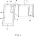
- FIG. 4 is a perspective view illustrating a lower mold according to an embodiment.
- FIG. 5 is a perspective view illustrating a state in which transparent substrates are put into the lower mold according to an embodiment.
- the lower mold may be used in operation 101.
- the lower mold 200 may include a cavity, which is a space in which a transparent substrate is formed.
- the cavity may include a first cavity 201 and a second cavity 202.
- the first cavity 201 and the second cavity 202 may be connected to each other.
- the first cavity 201 may have a first depth 201a.
- the second cavity 202 may have a second depth 202a.
- the second depth 202a may be greater than the first depth 201a.
- the shape of the cavities may have a shape different from the shape illustrated in FIGS. 4 and 5 . For example, referring to the cross section (A-A' section) of FIG.
- the second cavity 202 may further have a third depth 202b.
- the cavity may be defined to correspond to the shape of the transparent member to be formed.
- the first cavity 201 may have a shape corresponding to the shape of the thin film portion of the rear cover of the electronic device.
- the second cavity 202 may have a shape corresponding to a thick portion including a rear camera hole of the electronic device.
- the thick portion may refer to a portion protruding from the exterior of the electronic device compared to the thin film portion.
- the lower mold 200 may include a bottom portion, first and second sidewalls 204 and 205, and third and fourth sidewalls 206 and 207.
- the first sidewall 204 and the second sidewall 205 may face each other.
- the third sidewall 206 and the fourth sidewall 207 may face each other.
- At least one of the first sidewall 204, the second sidewall 205, the third sidewall 206, and the fourth sidewall 207 may have a curved shape.
- the sidewalls may include a curved shape that is seamlessly extended by being bent in a direction from the bottom portion toward the upper mold 400. For this reason, an edge of the transparent member thermoformed by the molds may include a curved portion.
- the cavities according to an embodiment may be spaces defined by at least some of the bottom portion, the first and second sidewalls 204 and 205, and the third and fourth sidewalls 206 and 207. Accordingly, a step may be present between the bottom portion corresponding to the first cavity 201 and the bottom portion corresponding to the second cavity 202.
- the lower mold 200 may include a one-sided core 203. This will be described later with reference to FIG. 6 .
- the transparent substrates in the process of putting the transparent substrates into the lower mold (101), the transparent substrates may be put into the lower mold.
- the first transparent substrate 301 and the second transparent substrate 302 may be separately put into the lower mold.
- the first transparent substrate 301 may be disposed in the first cavity 201.
- the second transparent substrate 302 may be disposed in the second cavity 202.
- the thickness of the first transparent substrate 301 according to an embodiment may be approximately 0.6 T.
- the thickness of the second transparent substrate 302 according to an embodiment may be approximately 2.85 T.
- the disclosure is not limited thereto.
- the first transparent substrate 301 and the second transparent substrate 302 may have the same color.
- the physical properties of the first transparent substrate 301 and the second transparent substrate 302 may be substantially the same.
- the transparent substrates can be translucent and have colors.
- the physical properties of the first transparent substrate 301 and the second transparent substrate 302 may be also different from each other.
- the physical properties thereof may be different from each other.
- the first transparent substrate 301 and the second transparent substrate 302 may be disposed such that a gap 210 is formed therebetween.
- the width of the gap 210 may increase from the inner side toward the outer side (e.g., in the +x-axis direction or the +y-axis direction in FIG. 5 ) with reference to the surface of the completed transparent member.
- the width of the gap 210 may increase toward a sidewall (e.g., the first sidewall 204) of the lower mold 200.
- the first transparent substrate 301 and the second transparent substrate 302 When the first transparent substrate 301 and the second transparent substrate 302 are disposed such that the width of the gap increases from the inner side to the outer side with reference to the plane on which the surface of the completed transparent member is disposed and the transparent substrates are melted, the first transparent substrate 301 and the second transparent substrate 302 may be bonded to each other from a portion having a smaller gap. Accordingly, it is possible to prevent pores, which would be generated due to the melting and boding of the transparent substrates, from being generated in the transparent member. The pores may be generated in at least one of the inside or the outside of the bonded portion in which the first transparent substrate 301 and the second transparent substrate 302 are bonded to each other.
- the region in which the first transparent substrate 301 and the second transparent substrate 302 face each other may be melted from the inner side by heating the transparent substrates from the centers of the cavities in which the transparent substrates are placed, respectively.
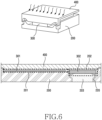
- FIG. 6 illustrates a perspective view and a cross-sectional view illustrating a process of disposing the upper mold and a process of preheating the molds according to an embodiment, which can be used during operation 103 of FIG. 3 .
- the upper mold 400 in the process of disposing the upper mold (103), the upper mold 400 may be disposed on the top surface of the transparent substrate 300.
- the upper mold 400 may include a pressing portion.
- the pressing portion may include at least one pressing surface corresponding to the lower mold 200.
- the pressing surface may have a shape of a protrusion including a curved edge.
- the disclosure is not limited thereto.
- the mold may be heated by an external heating member.
- the molds may be preheated by putting the molds into a thermoforming machine.
- the disclosure is not limited thereto.
- the pressing portion may include a heating mechanism that generates heat. As the pressing portion is heated by the heating mechanism, heat from the pressing portion may be transferred to the transparent substrate 300.
- the transparent substrate 300 may be melted by the heat.
- the transparent substrate 300 may have fluidity for thermoforming.
- the transparent substrate 300 with secured fluidity may flow along the inside of the mold (e.g., the lower mold 200).
- fluidity may be secured such that the first transparent substrate is capable of flowing along the inside of the first cavity 201.
- fluidity may be secured such that the second transparent substrate is capable of flowing along the inside of the second cavity 202.
- the lower mold 200 may include at least one air passage.
- the at least one air passage may be connected to the second cavity 202.
- the disclosure is not limited thereto.
- the lower mold 200 according to an embodiment may further include at least one one-sided core 203 disposed in the air passage.
- the one-sided core 203 may be connected to the second cavity 202.
- the disclosure is not limited thereto.
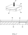
- the transparent substrate 300 in the process of thermoforming the transparent substrates by pressing the transparent substrates with the upper mold (107), the transparent substrate 300 may be pressed with the upper mold 400.
- the lower mold 200 and the upper mold 400 in which the transparent substrate 300 is disposed may be transferred to a press line or a press apparatus may be transferred to the molds to press the transparent substrate 300.
- the transparent substrate 300 may be pressed in a first direction 401.
- the disclosure is not limited thereto.
- the first transparent substrate (301 in FIG. 6 ) and the second transparent substrate (302 in FIG. 6 ) may be melted and bonded to each other.
- the first transparent substrate and the second transparent substrate which are bonded to each other may form one transparent member 500.
- the first transparent substrate 301 and the second transparent substrate 302 may be disposed such that the width of the gap therebetween increases from the inner side to the outer side with reference to the surface of the transparent member.
- the transparent substrates When the transparent substrates are melted, the transparent substrates may be bonded to each other starting from a portion in which the width of the gap is smaller. Accordingly, it is possible to prevent pores, which are generated when air is trapped in the process of melting and bonding the transparent substrates, from being generated in the transparent member.
- the thickness of a region corresponding to the first transparent substrate 301 may be 0.5T.
- the thickness of a region corresponding to the second transparent substrate 302 may be 2T.
- the disclosure is not limited thereto.
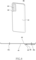
- FIG. 8 illustrates a cross-sectional view and a perspective view illustrating a transparent member according to an embodiment.
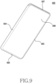
- FIG. 9 is a perspective view illustrating the inner surface of the transparent member according to an embodiment.
- the transparent substrate in the process of reinforcing the transparent substrate, may be reinforced.
- the reinforcing process may be performed at a temperature lower than a strain point of the transparent substrates and above a predetermined temperature.
- the disclosure is not limited thereto.
- a target surface compressive stress and reinforcing depth may be achieved in the transparent member.
- the transparent member 600 may include a first region 601, a second region 603, and a bonded portion 602.
- the first region 601 may have a first thickness 601a.
- the second region 603 may have a second thickness 603a. According to an embodiment, the second thickness 603a may be greater than the first thickness 601a.
- a difference in thickness between the first region 601 and the second region 603 may be within a range of 0.15 mm to 2.5 mm.
- the disclosure is not limited thereto.
- the first region 601 may have a plate shape.
- the second region 603 may have a shape protruding from a plane including the surface of the first region 601.
- the inner surface of the first region 601 and the inner surface of the second region 603 may include a plate shape.
- the disclosure is not limited thereto.
- the inner surface of the second region 603 may be concave (not illustrated) to face the protruding direction.
- a camera module of the electronic device may be inserted into the concave portion.
- the camera module of the electronic device may be protected by being inserted into the protruding portion.
- the concave portion allows the camera module to be inserted thereinto, thereby preventing the camera module from excessively protruding from the rear plate of the electronic device.
- the first region 601 and the second region 603 may be at least partially melted and bonded to each other. It shall be understood that melting and bonding of the first region 601 and the second region 603 result in different structural characteristics from a similarly shaped transparent member 600, formed as one piece.
- the first region 601 may have structural properties similar to the first transparent substrate 301 and the second region 603 may have structural properties that are similar to the second transparent substrate 302.
- the bonded portion 602 may be formed the first transparent substrate 301 and the second transparent substrate 302 are melted and bonded to each other.
- the bonded portion 602 may refer to a portion in which the first transparent substrate 301 and the second transparent substrate 302 are melted and bonded to each other.
- the transparent member 600 may be translucent or include at least one color.
- the first region 601 may include a first color.
- the second region 603 may include a second color.
- the bonded portion 602 may include a mixture of the first color and the second color, or a third color that results from mixing the first color and the second color.
- the transparent member formed through the transparent member forming method (100) may include one or more microbubbles.
- the one or more microbubbles may be formed in the bonded portion 602.
- the microbubbles may be formed during short-time thermoforming.
- the microbubbles may be formed in the entire region of the bonded portion 602. Accordingly, when the width of the gap increases from the inner side to the outer side with reference to the surface of the completed transparent member, it is possible to prevent the microbubbles from being formed in the entire region of the bonded portion.
- the size of the microbubbles may be smaller than 200 um. According to an embodiment, the size of the microbubbles may be 0 to 10 um. Accordingly, the microbubbles may be observed with a microscope. However, the disclosure is not limited thereto.
- the side portions may include a curved surface.
- the first side portion 604 and the second side portion 605 may be bent from the first region (601 in FIG. 8 ) toward the inner surface 608 of the transparent member 600 to extend seamlessly.
- the third side portion 606 and the fourth side portion 607 may be bent from the first region (601 in FIG. 9 ) to extend seamlessly in a direction in which the inner surface 608 of the transparent member 600 is oriented.
- the electronic device may include the transparent member 600.
- the transparent member 600 may be referred to by a transparent member 500 formed through the transparent member forming method (100) of FIGS. 3 to 7 .
- the same reference numerals are used for the same or substantially the same components as those described above, and overlapping descriptions will be omitted.
Landscapes
- Engineering & Computer Science (AREA)
- Chemical & Material Sciences (AREA)
- Materials Engineering (AREA)
- Organic Chemistry (AREA)
- Mechanical Engineering (AREA)
- Microelectronics & Electronic Packaging (AREA)
- Signal Processing (AREA)
- Devices For Indicating Variable Information By Combining Individual Elements (AREA)
Description
- Various embodiments disclosed herein relate to a method of thermoforming a transparent member.
- An electronic device may have an angular shape as well as a curved edge portion to improve aesthetics. Alternatively, an electronic device may have a surface that has a plurality of heights in order to dispose components (e.g., a camera) of the electronic device. In addition, at least one surface of the electronic device may have glass. The glass protects the external portion of the electronic device. The glass formed on the external portion of the electronic device may have a shape corresponding to the shape of the surfaces of the electronic device.
- The shape of the glass may be made by using a polishing method of manufacturing a curved surface by grinding the glass surface with a grinder, or by using a thermoforming method of heating glass and then bending or pressing the glass to form the glass.
- In the case of forming glass using the thermoforming method, flat glass may be placed between upper and lower molds. The molds are pressed at a certain temperature and pressure. The foregoing produces glass corresponding to the shape of a cavity defined in the molds.
-
CN106746526 A teaches a method for forming three-dimensional glass substrates by pressing several of them at once using a lower mold with several cavities and a corresponding upper mold. A corresponding teaching as inCN106746526 A is also disclosed inKR20180085522 A US2017349472 A1 . - As a glass forming method used in an electronic device, a method of grinding a glass surface such as a Computerized Numerical Control (CNC) process may be used. By the forming method performed through the grinding, a CNC tool mark, a step, or thermoforming wrinkles may occur on the glass. Accordingly, the surface quality of the glass may deteriorate. In addition, a post-process (e.g., a polishing process) for improving the surface quality may be required. Therefore, the manufacturing cost is increased, and the forming time is long, which may cause a problem in that the productivity is decreased.
- Various embodiments disclosed herein are able to provide a transparent member including bending glass including a curved surface or glass having a partially asymmetric shape in the thickness of one surface, and a method of thermoforming the transparent member with molds.
- A transparent member forming method according to various embodiments of the disclosure includes, as defined in claim 1: a process of putting a first transparent substrate and a second transparent substrate into a first cavity of a lower mold that has a first depth and a second cavity of a lower mold that is connected to the first cavity and has a second depth, respectively; a process of disposing an upper mold, which corresponds to the lower mold and includes a pressing portion having at least one pressing surface, on an upper portion of the lower mold; a process of preheating at least one of the lower mold in which the transparent substrates are disposed or the upper mold to a predetermined temperature; and a process of thermoforming the preheated transparent substrates by pressing the preheated transparent substrates in a manner of pressing the upper mold.
- According to various embodiments disclosed herein, it is possible to provide a transparent member formed through a thermoforming process using molds without a separate CNC process and a method for thermoforming a transparent member. Due to this, the time required for a CNC machining process and a polishing process for removing a CNC tool mark may be reduced.
- In addition, according to various embodiments, transparent substrates corresponding a thick portion and a thin film portion are separately put into a transparent member thermoforming mold, and the respective transparent substrates are bonded to each other during thermoforming. Therefore, it is possible to implement a curved shape or a shape having a partially different thickness on one surface.
- Furthermore, according to various embodiments, since the lower mold includes at least one air passage, it is possible to prevent pores, which are generated melting and bonding of the transparent substrates, from being formed in the transparent member.
- In addition, various effects directly or indirectly identified through the disclosure may be provided.
-
-
FIG. 1 is a front perspective view of an electronic device according to an embodiment. -
FIG. 2 is a rear perspective view of the electronic device according to an embodiment. -
FIG. 3 is a flowchart illustrating a transparent member forming method according to an embodiment. -
FIG. 4 is a perspective view illustrating a lower mold according to an embodiment. -
FIG. 5 is a perspective view illustrating a state in which transparent substrates are put into the lower mold according to an embodiment. -
FIG. 6 illustrates a perspective view and a cross-sectional view illustrating a process of disposing the upper mold and a process of preheating the molds according to an embodiment. -
FIG. 7 illustrates a perspective view and a cross-sectional view illustrating a process of pressing the transparent substrate with the upper mold to thermoforming the transparent substrates according to an embodiment. -
FIG. 8 illustrates a cross-sectional view and a perspective view illustrating a transparent member according to an embodiment. -
FIG. 9 is a perspective view illustrating the inner surface of the transparent member according to an embodiment. - In connection with the description of the drawings, the same or similar components may be denoted by the same or similar reference numerals.
- According to certain embodiments disclosed herein, it is possible to provide a transparent member formed through a thermoforming process using molds without a separate CNC process and a method for thermoforming a transparent member. Due to this, the time required for a CNC machining process and a polishing process for removing a CNC tool mark may be reduced.
- In addition, according to certain embodiments, transparent substrates corresponding a thick portion and a thin film portion are separately put into a transparent member thermoforming mold, and the respective transparent substrates are bonded to each other during thermoforming. Therefore, it is possible to implement a curved shape or a shape having a partially different thickness on one surface.
- Furthermore, according to certain embodiments, since the lower mold includes at least one air passage, it is possible to prevent pores, which are generated melting and bonding of the transparent substrates, from being formed in the transparent member.
- In addition, various effects directly or indirectly identified through the disclosure may be provided.
- Hereinafter, various embodiments of the disclosure will be described in detail with reference to the accompanying drawings.
- An electronic device according to various embodiments of the disclosure may include at least one of, for example, a smartphone, a tablet personal computer (PC), a mobile phone, a video phone, an electronic book reader (e-book reader), a desktop PC, a laptop PC, a netbook computer, a workstation, a server, a personal digital assistant (PDA), a portable multimedia player (PMP), a MPEG-1 audio layer-3 (MP3) player, a mobile medical device, a camera, and a wearable device. The wearable device may include at least one of an accessory type (e.g., watch, ring, bracelet, anklet, necklace, glasses, contact lens, or head-mounted device (HMD)), a fabric or clothing-integrated type (e.g., electronic clothing), a body-mounted type (e.g., skin pad, or tattoo), and a bio-implantable type (e.g., implantable circuit).
- According to some embodiments, the electronic device may include at least one of, for example, a television, a digital video disk (DVD) player, an audio, a refrigerator, an air conditioner, a vacuum cleaner, an oven, a microwave oven, a washing machine, an air purifier, a set-top box, a home automation control panel, a security control panel, a TV box, a game console, an electronic dictionary, an electronic key, a camcorder, and an electronic photo frame.
- According to other embodiments, the electronic device may include at least one of various medical devices (e.g., various portable medical measuring devices (blood glucose monitoring device, heart rate monitoring device, blood pressure measuring device, body temperature measuring device, etc.), magnetic resonance angiography (MRA), magnetic resonance imaging (MRI), computed tomography (CT) machine, ultrasonic machine, etc.), a navigation device, a global positioning system (GPS) receiver, an event data recorder (EDR) , a flight data recorder (FDR) , a vehicle infotainment device, electronic equipment for a ship (e.g., ship navigation device, gyro-compass, etc.), avionics, a security device, an automobile head unit, a home or industrial robot, an automatic teller's machine (ATM) in banks, point of sales (POS) in a shop, or Internet of things devices (e.g., light bulb, various sensors, electric or gas meter, sprinkler device, fire alarm, thermostat, streetlamp, toaster, sporting goods, hot water tank, heater, boiler, etc.).
- According to some embodiments, the electronic device may include at least one of a part of furniture or a building/structure, an electronic board, an electronic signature receiving device, a projector, and various kinds of measuring instruments (e.g., water meter, electric meter, gas meter, radio wave meter, etc.). In various embodiments, the electronic device may be a combination of one or more of the aforementioned various devices. According to some embodiments, the electronic device may also be a flexible device. Further, the electronic device according to an embodiment of the disclosure is not limited to the aforementioned devices, and may include a new electronic device according to the development of technology.
-
FIG. 1 is a front perspective view of anelectronic device 1500 according to an embodiment, andFIG. 2 is a rear perspective view of theelectronic device 1500 according to an embodiment. - Referring to
FIGS. 1 and2 , according to an embodiment, theelectronic device 1500 may include ahousing 1510 including a first surface (or a front surface) 1510A, a second surface (or a rear surface) 1510B, and aside surface 1510C surrounding the space between thefirst surface 1510A and thesecond surface 1510B. In another embodiment (not illustrated), the housing may mean a structure defining some of thefirst surface 1510A ofFIG. 1 , thesecond surface 1510B, and theside surface 1510C ofFIG. 2 . According to an embodiment, at least a portion of thefirst surface 1510A may be defined by a substantially transparent front plate 1502 (e.g., a glass plate or a polymer plate including various coating layers as the front plate). In another embodiment, thefront plate 1502 may be coupled to thehousing 1510 so as to define an inner space with thehousing 1510. In various embodiments, the term "internal space" may mean a space accommodating at least a portion of thedisplay 1501 as an internal space of thehousing 1510. - According to various embodiments, the
second surface 1510B may be defined by a substantially opaquerear plate 1511. Therear plate 1511 may be made of, for example, coated or colored glass, ceramic, polymer, metal (e.g., aluminum, stainless steel (STS), or magnesium), or a combination of two or more of these materials. Theside surface 1510C may be provided by a side bezel structure (or a "side member") 1518 coupled to thefront plate 1502 and therear plate 1511 and including a metal and/or a polymer. In various embodiments, therear plate 1511 and theside bezel structure 1518 may be integrally configured, and may include the same material (e.g., a metal material such as aluminum). - In the illustrated embodiment, the
front plate 1502 may include twofirst regions 1510D (e.g., curved regions), which are bent from thefirst surface 1510A toward therear plate 1511 and extend seamlessly, at the long opposite side edges thereof. In the illustrated embodiment, therear plate 1511 may include twosecond regions 1510E (e.g., curved regions), which are bent from thesecond face 1510B toward thefront plate 1502 and extend seamlessly, at the long opposite side edges thereof. In various embodiments, the front plate 1502 (or the rear plate 1511) may include only one of thefirst regions 1510D (or thesecond regions 1510E). In another embodiment, some of thefirst regions 1510D or thesecond regions 1510E may not be included. In the above-described embodiments, when viewed from a side of theelectronic device 1500, theside bezel structure 1518 may have a first thickness (or width) on the side surface in which thefirst regions 1510D or thesecond regions 1510E are not included (e.g., the side surface in which theconnector hole 1508 is disposed), and may have a second thickness, which is smaller than the first thickness, on the side surface in which thefirst regions 1510D or thesecond regions 1510E are included (e.g., the side surfaces in which thekey input devices 1517 are disposed). - According to an embodiment, the
electronic device 1500 may include at least one of adisplay 1501,audio modules sensor modules 1504,camera modules key input devices 1517, light-emittingelements 1506, andconnector holes key input devices 1517 or the light-emitting elements 1506) may be omitted from theelectronic device 1500, or theelectronic device 1500 may additionally include other components. - The
display 1501 may be visually exposed through, for example, a considerable portion of thefront plate 1502. In various embodiments, at least a portion of thedisplay 1501 may be visually exposed through thefront plate 1502 defining thefirst surface 1510A and thefirst regions 1510D of the side surfaces 1510C. In various embodiments, the edges of thedisplay 1501 may be configured to be substantially the same as the contour shape of thefront plate 1502 adjacent thereto. In another embodiment (not illustrated), the distance between the periphery of thedisplay 1501 and the periphery of thefront plate 1502 may be substantially constant in order to increase the exposed area of thedisplay 1501. - In another embodiment (not illustrated), recesses or openings may be provided in a portion of a screen display region (e.g., an active region) or a region (e.g., a non-active region) out of the screen display region of the
display 1501, and at least one of theaudio module 1514, thesensor modules 1504, thecamera modules elements 1506, which are aligned with the recesses or the openings, may be included. In another embodiment (not illustrated), the rear surface of the screen display region of thedisplay 1501 may include at least one of theaudio module 1514, thesensor modules 1504, thecamera modules elements 1506. In another embodiment (not illustrated), thedisplay 1501 may be coupled to or disposed adjacent to a touch-sensing circuit, a pressure sensor capable of measuring the intensity of a touch (pressure), and/or a digitizer that detects an electromagnetic-field-type stylus pen. In some embodiments, at least some of thesensor modules 1504 and/or at least some of thekey input devices 1517 may be disposed in thefirst regions 1510D and/or thesecond regions 1510E. - The
audio modules microphone hole 1503 andspeaker holes microphone hole 1503 may include a microphone disposed therein so as to acquire external sound, and in various embodiments, multiple microphones may be disposed therein so as to detect the direction of sound. The speaker holes 1507 and 1514 may include anexternal speaker hole 1507 and acall receiver hole 1514. In various embodiments, the speaker holes 1507 and 1514 and themicrophone hole 1503 may be implemented as a single hole, or a speaker (e.g., a piezo speaker) may be included without the speaker holes 1507 and 1514. - The
sensor module 1504 may generate electrical signals or data values corresponding to the internal operating states or the external environmental states of theelectronic device 1500. Thesensor modules 1504 may include, for example, a first sensor module 1504 (e.g., a proximity sensor), a second sensor module (not illustrated) (e.g., a fingerprint sensor) disposed on thefirst surface 1510A of thehousing 1510, and/or another sensor module (not illustrated) (e.g., an HRM sensor or a fingerprint sensor) disposed on thesecond surface 1510B of thehousing 1510. The fingerprint sensor may be disposed not only on thefirst surface 1510A (e.g., the display 1501) of thehousing 1510, but also on thesecond surface 1510B. Theelectronic device 1500 may further include at least one of sensor modules (not illustrated), such as a gesture sensor, a gyro sensor, an atmospheric pressure sensor, a magnetic sensor, an acceleration sensor, a grip sensor, a color sensor, an infrared (IR) sensor, a biometric sensor, a temperature sensor, a humidity sensor, or an illuminance sensor. - The
camera modules first camera device 1505 disposed on thefirst surface 1510A of theelectronic device 1500 and asecond camera device 1555 disposed on thesecond surface 1510B of theelectronic device 1500. Thecamera modules second surface 1510B. The flash may include, for example, a light-emitting diode or a xenon lamp. In various embodiments, two or more lenses (e.g., an infrared camera lens, a wide-angle lens, and a telephoto lens) and image sensors may be disposed on one surface of theelectronic device 1500. - The
key input devices 1517 may be disposed on theside surface 1510C of thehousing 1510. In another embodiment, theelectronic device 1500 may not include some or all of the above-mentionedkey input devices 1517, and akey input device 1517, which is not included in the above mentioned key input devices, may be implemented in another form, like a soft key, on thedisplay 1501. - The light-emitting
elements 1506 may be disposed, for example, on thefirst surface 1510A of thehousing 1510. The light-emittingelements 1506 may provide, for example, information about the state of theelectronic device 1500 in an optical form. In another embodiment, the light-emittingelements 1506 may provide a light source that is interlocked with, for example, the operation of thecamera modules 1505. Thelight emitting elements 1506 may include, for example, an LED, an IR LED, and a xenon lamp. - The connector holes 1508 and 1509 may include a
first connector hole 1508, which is capable of accommodating a connector (e.g., a USB connector) for transmitting/receiving power and/or data to/from an external electronic device, and/or asecond connector hole 1509, which is capable of accommodating a connector (e.g., an earphone jack) for transmitting/receiving an audio signal to/from an external electronic device. - As a glass forming method used in an electronic device, a method of grinding a glass surface such as a Computerized Numerical Control (CNC) process may be used. By the forming method performed through the grinding, a CNC tool mark, a step, or thermoforming wrinkles may occur on the glass. Accordingly, the surface quality of the glass may deteriorate. In addition, a post-process (e.g., a polishing process) for improving the surface quality may be required. This increases the manufacturing costs and production time.
- Certain embodiments disclosed herein are able to provide a transparent member including bending glass including a curved surface or glass having a partially asymmetric shape in the thickness of one surface, and a method of thermoforming the transparent member with molds.
-
FIG. 3 is a flowchart illustrating a method of forming a transparent member according to an embodiment. - Referring to
FIG. 3 , a transparent member forming method (100) according to an embodiment may include a process of putting a transparent substrate into a lower mold (101), a process of disposing an upper mold (103), a process of preheating the molds (105), and a process of thermoforming the transparent substrates by pressing the upper mold (107). - According to an embodiment, in the process of putting the transparent substrates into the lower mold (101), the plurality of transparent substrates may be put into the lower mold. For example, the plurality of transparent substrates may be put respectively into a plurality of cavities in the lower mold. The plurality of transparent substrates put into the cavities may be formed in at least one of the process of preheating the molds (105) or the process of thermoforming the transparent substrates by pressing the upper mold (107). However, the disclosure is not limited thereto.
- According to various embodiments, the transparent
member forming method 100 may further include one or more other processes. For example, the transparent member forming method (100) may further include at least one of a process of polishing at least a portion of one surface of each of the thermoformed transparent substrates or a process of reinforcing the thermoformed transparent substrates. According to an embodiment, a process of reinforcing the transparent substrates may be performed after the polishing process. According to an embodiment, the polishing process may be performed on a part or all of the surface of the transparent member according to an intended use of the transparent member. The external roughness and strength of the transparent member may be improved due to the polishing process. However, the disclosure is not limited thereto. Specific details of each process of the transparent member forming method (100) according to an embodiment will be described later. - According to an embodiment, the transparent substrates may include at least one of soda-lime glass, glass containing lead monoxide in a lead glass composition (lead-alkali glass), borosilicate glass, aluminosilicate glass, or silica glass. However, the disclosure is not limited thereto. For example, the transparent substrates are used for a display or a cover of an electronic device and may include various members having a thermoplastic property.
-
FIG. 4 is a perspective view illustrating a lower mold according to an embodiment.FIG. 5 is a perspective view illustrating a state in which transparent substrates are put into the lower mold according to an embodiment. The lower mold may be used inoperation 101. - Referring to
FIGS. 4 and5 , thelower mold 200 according to an embodiment may include a cavity, which is a space in which a transparent substrate is formed. According to an embodiment, the cavity may include afirst cavity 201 and asecond cavity 202. Thefirst cavity 201 and thesecond cavity 202 may be connected to each other. Thefirst cavity 201 may have afirst depth 201a. Thesecond cavity 202 may have asecond depth 202a. Thesecond depth 202a may be greater than thefirst depth 201a. However, according to another embodiment, the shape of the cavities may have a shape different from the shape illustrated inFIGS. 4 and5 . For example, referring to the cross section (A-A' section) ofFIG. 5 , thesecond cavity 202 may further have athird depth 202b. According to various embodiments, the cavity may be defined to correspond to the shape of the transparent member to be formed. For example, thefirst cavity 201 may have a shape corresponding to the shape of the thin film portion of the rear cover of the electronic device. Thesecond cavity 202 may have a shape corresponding to a thick portion including a rear camera hole of the electronic device. However, the disclosure is not limited thereto. The thick portion may refer to a portion protruding from the exterior of the electronic device compared to the thin film portion. - According to an embodiment, the
lower mold 200 may include a bottom portion, first andsecond sidewalls fourth sidewalls first sidewall 204 and thesecond sidewall 205 may face each other. Thethird sidewall 206 and thefourth sidewall 207 may face each other. - According to an embodiment, at least one of the
first sidewall 204, thesecond sidewall 205, thethird sidewall 206, and thefourth sidewall 207 may have a curved shape. For example, the sidewalls may include a curved shape that is seamlessly extended by being bent in a direction from the bottom portion toward theupper mold 400. For this reason, an edge of the transparent member thermoformed by the molds may include a curved portion. - The cavities according to an embodiment may be spaces defined by at least some of the bottom portion, the first and
second sidewalls fourth sidewalls first cavity 201 and the bottom portion corresponding to thesecond cavity 202. - According to an embodiment, the
lower mold 200 may include a one-sided core 203. This will be described later with reference toFIG. 6 . - According to an embodiment, in the process of putting the transparent substrates into the lower mold (101), the transparent substrates may be put into the lower mold. According to an embodiment, the first
transparent substrate 301 and the secondtransparent substrate 302 may be separately put into the lower mold. For example, the firsttransparent substrate 301 may be disposed in thefirst cavity 201. The secondtransparent substrate 302 may be disposed in thesecond cavity 202. - The thickness of the first
transparent substrate 301 according to an embodiment may be approximately 0.6 T. The thickness of the secondtransparent substrate 302 according to an embodiment may be approximately 2.85 T. However, the disclosure is not limited thereto. - According to an embodiment, the first
transparent substrate 301 and the secondtransparent substrate 302 may have the same color. In this case, the physical properties of the firsttransparent substrate 301 and the secondtransparent substrate 302 may be substantially the same. However, the disclosure is not limited thereto. For example, the transparent substrates can be translucent and have colors. When the colors of the firsttransparent substrate 301 and the secondtransparent substrate 302 are different from each other, the physical properties of the firsttransparent substrate 301 and the secondtransparent substrate 302 may be also different from each other. Furthermore, when the firsttransparent substrate 301 and the secondtransparent substrate 302 are different from each other in required strength or refractive index, the physical properties thereof may be different from each other. - According to an embodiment, in the process of putting the transparent substrates into the lower mold (101), the first
transparent substrate 301 and the secondtransparent substrate 302 may be disposed such that agap 210 is formed therebetween. Referring to the enlarged view ofFIG. 5 , the width of thegap 210 according to an embodiment may increase from the inner side toward the outer side (e.g., in the +x-axis direction or the +y-axis direction inFIG. 5 ) with reference to the surface of the completed transparent member. For example, the width of thegap 210 may increase toward a sidewall (e.g., the first sidewall 204) of thelower mold 200. - When the first
transparent substrate 301 and the secondtransparent substrate 302 are disposed such that the width of the gap increases from the inner side to the outer side with reference to the plane on which the surface of the completed transparent member is disposed and the transparent substrates are melted, the firsttransparent substrate 301 and the secondtransparent substrate 302 may be bonded to each other from a portion having a smaller gap. Accordingly, it is possible to prevent pores, which would be generated due to the melting and boding of the transparent substrates, from being generated in the transparent member. The pores may be generated in at least one of the inside or the outside of the bonded portion in which the firsttransparent substrate 301 and the secondtransparent substrate 302 are bonded to each other. - As another example, in the process of applying heat to the transparent substrates inside the mold, the region in which the first
transparent substrate 301 and the secondtransparent substrate 302 face each other may be melted from the inner side by heating the transparent substrates from the centers of the cavities in which the transparent substrates are placed, respectively. -
FIG. 6 illustrates a perspective view and a cross-sectional view illustrating a process of disposing the upper mold and a process of preheating the molds according to an embodiment, which can be used duringoperation 103 ofFIG. 3 . - According to an embodiment, in the process of disposing the upper mold (103), the
upper mold 400 may be disposed on the top surface of thetransparent substrate 300. According to an embodiment, theupper mold 400 may include a pressing portion. The pressing portion may include at least one pressing surface corresponding to thelower mold 200. For example, the pressing surface may have a shape of a protrusion including a curved edge. However, the disclosure is not limited thereto. - According to an embodiment, at least one of the
lower mold 200 or theupper mold 400 is at least one of cold steel tool dice (STD), zirconium 03 (ZrO3), aluminum 203 (Al2O3), or titanium (Titanium). However, the disclosure is not limited thereto. For example, the molds may include a material having high thermal conductivity, such as graphite or stainless steel (STS). As a result, the mold including the pressing portion may heat thetransparent substrate 300. - According to an embodiment, in the process of preheating the mold (105), at least one of the
lower mold 200 and theupper mold 400 may be preheated to a predetermined temperature for a predetermined period of time. For example, the thermoforming process may be performed at a temperature equal to or higher than the softening point of thetransparent substrate 300. According to an embodiment, a transparent substrate with a softening point of 1100°C/2012°F or higher may be used. However, the disclosure is not limited thereto. - According to an embodiment, the mold may be heated by an external heating member. For example, the molds may be preheated by putting the molds into a thermoforming machine. However, the disclosure is not limited thereto. For example, the pressing portion may include a heating mechanism that generates heat. As the pressing portion is heated by the heating mechanism, heat from the pressing portion may be transferred to the
transparent substrate 300. - According to an embodiment, the
transparent substrate 300 may be melted by the heat. For example, when at least one of thelower mold 200 or theupper mold 400 is heated to a predetermined temperature, thetransparent substrate 300 may have fluidity for thermoforming. Thetransparent substrate 300 with secured fluidity may flow along the inside of the mold (e.g., the lower mold 200). For example, after the temperature of the firsttransparent substrate 301 is increased, fluidity may be secured such that the first transparent substrate is capable of flowing along the inside of thefirst cavity 201. After the temperature of the secondtransparent substrate 302 is increased, fluidity may be secured such that the second transparent substrate is capable of flowing along the inside of thesecond cavity 202. - According to an embodiment, the
lower mold 200 may include at least one air passage. The at least one air passage may be connected to thesecond cavity 202. However, the disclosure is not limited thereto. Referring toFIG. 6 , thelower mold 200 according to an embodiment may further include at least one one-sided core 203 disposed in the air passage. The one-sided core 203 may be connected to thesecond cavity 202. However, the disclosure is not limited thereto. - According to an embodiment, the one-
sided core 203 may be separated from thelower mold 200. For example, the one-sided core 203 may be manufactured separately from thelower mold 200 and assembled to thelower mold 200. Accordingly, referring toFIG. 6 , at least onegap 220 may be formed between thelower mold 200 and the one-sided core 203. In at least one of the process of preheating the mold (105) or the process of thermoforming the transparent substrates by pressing the transparent substrates with the upper mold (107), when thetransparent substrate 300 is melted, air may be discharged through thegap 220. Since the air is discharged through the at least one air passage or thegap 220, it is possible to prevent pores from being generated in the transparent member due to an air trap phenomenon. -
FIG. 7 illustrates a perspective view and a cross-sectional view illustrating a process of pressing the transparent substrate with the upper mold to thermoforming the transparent substrates according to an embodiment. - The pressing may mean, for example, applying a load from no load (0 kgf) to 100 kgf or more.
- According to an embodiment, in the process of thermoforming the transparent substrates by pressing the transparent substrates with the upper mold (107), the
transparent substrate 300 may be pressed with theupper mold 400. For example, thelower mold 200 and theupper mold 400 in which thetransparent substrate 300 is disposed may be transferred to a press line or a press apparatus may be transferred to the molds to press thetransparent substrate 300. Referring toFIG. 7 , thetransparent substrate 300 may be pressed in afirst direction 401. However, the disclosure is not limited thereto. - According to an embodiment, by this pressing operation, the
transparent substrate 300 may be deformed by the pressure applied from theupper mold 400. Accordingly, thetransparent substrate 300 may be molded to correspond to the shape of the cavity of thelower mold 200. For example, the firsttransparent substrate 301 may be formed to correspond to the shape of thefirst cavity 201. The secondtransparent substrate 302 may be formed to correspond to the shape of thesecond cavity 202. Due to the shapes of thelower mold 200 and theupper mold 400, the edge of thetransparent member 500 may include a curved shape. - According to an embodiment, in at least one of the process of preheating the molds (105) or the process of thermoforming the transparent substrates by pressing the transparent substrates with the upper mold (107), the first transparent substrate (301 in
FIG. 6 ) and the second transparent substrate (302 inFIG. 6 ) may be melted and bonded to each other. The first transparent substrate and the second transparent substrate which are bonded to each other may form onetransparent member 500. - According to an embodiment, the first
transparent substrate 301 and the secondtransparent substrate 302 may be disposed such that the width of the gap therebetween increases from the inner side to the outer side with reference to the surface of the transparent member. When the transparent substrates are melted, the transparent substrates may be bonded to each other starting from a portion in which the width of the gap is smaller. Accordingly, it is possible to prevent pores, which are generated when air is trapped in the process of melting and bonding the transparent substrates, from being generated in the transparent member. - According to an embodiment, in the
transparent member 500 thermoformed by being pressed, the thickness of a region corresponding to the firsttransparent substrate 301 may be 0.5T. In addition, in thetransparent member 500, the thickness of a region corresponding to the secondtransparent substrate 302 may be 2T. However, the disclosure is not limited thereto. -
FIG. 8 illustrates a cross-sectional view and a perspective view illustrating a transparent member according to an embodiment.FIG. 9 is a perspective view illustrating the inner surface of the transparent member according to an embodiment. - The
transparent member 600 may be referred to by thetransparent member 500 formed through the transparent member forming method (100) ofFIGS. 3 to 7 . The same reference numerals are used for the same or substantially the same components as those described above, and overlapping descriptions will be omitted. - A
transparent member 600 according to an embodiment may be formed by the transparent member forming method (100). For example, thetransparent member 600 may be formed by performing a process of putting transparent substrates into a lower mold (101 inFIG. 3 ), a process of disposing an upper mold (103 inFIG. 3 ), a process of preheating the mold (105 inFIG. 3 ), and a process of thermoforming the transparent substrates by pressing the upper mold (107 inFIG. 3 ). However, the disclosure is not limited thereto. For example, thetransparent member 600 may be further subjected to a polishing process on at least a portion of one surface of each of the thermoformed transparent substrates. As another example, thetransparent member 600 may be further subjected to a process of reinforcing the transparent substrates after the thermoforming process. - According to an embodiment, in the process of reinforcing the transparent substrate, the transparent substrate may be reinforced. For example, the reinforcing process may be performed at a temperature lower than a strain point of the transparent substrates and above a predetermined temperature. However, the disclosure is not limited thereto. Through the reinforcing process, a target surface compressive stress and reinforcing depth may be achieved in the transparent member.
- Referring to
FIG. 8 , thetransparent member 600 according to an embodiment may include afirst region 601, asecond region 603, and a bondedportion 602. Thefirst region 601 may have afirst thickness 601a. Thesecond region 603 may have asecond thickness 603a. According to an embodiment, thesecond thickness 603a may be greater than thefirst thickness 601a. - According to an embodiment, a difference in thickness between the
first region 601 and thesecond region 603 may be within a range of 0.15 mm to 2.5 mm. However, the disclosure is not limited thereto. - According to an embodiment, the
first region 601 may have a plate shape. Thesecond region 603 may have a shape protruding from a plane including the surface of thefirst region 601. According to an embodiment, the inner surface of thefirst region 601 and the inner surface of thesecond region 603 may include a plate shape. However, the disclosure is not limited thereto. For example, the inner surface of thesecond region 603 may be concave (not illustrated) to face the protruding direction. According to an embodiment, a camera module of the electronic device may be inserted into the concave portion. The camera module of the electronic device may be protected by being inserted into the protruding portion. Furthermore, the concave portion allows the camera module to be inserted thereinto, thereby preventing the camera module from excessively protruding from the rear plate of the electronic device. - In the bonded
portion 602 according to an embodiment, thefirst region 601 and thesecond region 603 may be at least partially melted and bonded to each other. It shall be understood that melting and bonding of thefirst region 601 and thesecond region 603 result in different structural characteristics from a similarly shapedtransparent member 600, formed as one piece. Specifically thefirst region 601 may have structural properties similar to the firsttransparent substrate 301 and thesecond region 603 may have structural properties that are similar to the secondtransparent substrate 302. Referring toFIG. 6 , the bondedportion 602 may be formed the firsttransparent substrate 301 and the secondtransparent substrate 302 are melted and bonded to each other. For example, the bondedportion 602 may refer to a portion in which the firsttransparent substrate 301 and the secondtransparent substrate 302 are melted and bonded to each other. - According to an embodiment, the
transparent member 600 may be translucent or include at least one color. For example, thefirst region 601 may include a first color. Thesecond region 603 may include a second color. The bondedportion 602 may include a mixture of the first color and the second color, or a third color that results from mixing the first color and the second color. - The transparent member formed through the transparent member forming method (100) according to an embodiment may include one or more microbubbles. For example, the one or more microbubbles may be formed in the bonded
portion 602. The microbubbles may be formed during short-time thermoforming. - According to an embodiment, in the process of putting the transparent substrates of
FIG. 3 into the lower mold (101), when the width of the gap (210 inFIG. 3 ) between the first transparent substrate (301 inFIG. 5 ) and the second transparent substrate (302 inFIG. 3 ) is constant, the microbubbles may be formed in the entire region of the bondedportion 602. Accordingly, when the width of the gap increases from the inner side to the outer side with reference to the surface of the completed transparent member, it is possible to prevent the microbubbles from being formed in the entire region of the bonded portion. - According to an embodiment, the size of the microbubbles may be smaller than 200 um. According to an embodiment, the size of the microbubbles may be 0 to 10 um. Accordingly, the microbubbles may be observed with a microscope. However, the disclosure is not limited thereto.
- Referring to
FIG. 9 , thetransparent member 600 according to an embodiment may include one or more side portions. For example, the edges of thetransparent member 600 may include afirst side portion 604, asecond side portion 605, athird side portion 606, and afourth side portion 607. Thefirst side portion 604 and thesecond side portion 605 may face each other. Thethird side portion 606 and thefourth side portion 607 may face each other. - The side portions according to an embodiment may include a curved surface. For example, the
first side portion 604 and thesecond side portion 605 may be bent from the first region (601 inFIG. 8 ) toward theinner surface 608 of thetransparent member 600 to extend seamlessly. Thethird side portion 606 and thefourth side portion 607 may be bent from the first region (601 inFIG. 9 ) to extend seamlessly in a direction in which theinner surface 608 of thetransparent member 600 is oriented. - According to an embodiment, the electronic device (e.g., the electronic device 10 in
FIG. 1 ) may include thetransparent member 600. Thetransparent member 600 may be referred to by atransparent member 500 formed through the transparent member forming method (100) ofFIGS. 3 to 7 . The same reference numerals are used for the same or substantially the same components as those described above, and overlapping descriptions will be omitted. - According to an embodiment, the electronic device may include a display, a rear cover, and a side housing. The rear cover may be disposed on a surface opposite to the display. The side housing may be provided to surround the space between the display and the rear cover. However, the configuration of the electronic device is not limited thereto. According to an embodiment, at least one of the above-described components may be omitted from the electronic device, or the electronic device may further include one or more other components. For example, the electronic device may further include a camera device disposed on the rear cover.
- Referring to
FIG. 8 , thetransparent member 600 according to an embodiment may configure at least a portion of the rear cover of the electronic device. For example, thefirst region 601 may be at least a portion of the rear plate of the electronic device. For example, thefirst region 601 may be a portion of the rear plate (1511 inFIG. 2 ) of the electronic device (1500 inFIG. 1 ). Thesecond region 603 may be at least a portion of a thick portion in which the rear camera of the electronic device is located. For example, thesecond region 603 may be a portion of the camera module (1555 inFIG. 2 ) of the electronic device (1500 inFIG. 1 ). However, the disclosure is not limited thereto. For example, thetransparent member 600 according to an embodiment may be used not only for an exterior of an electronic device including a smartphone (e.g., theelectronic device 1500 inFIG. 1 ), but also for an exterior of any of various types of electronic devices such as a tablet personal computer (PC), a wearable device, or a home appliance (e.g., a refrigerator, a microwave oven, a washing machine, or an audio system). - Various embodiments of the disclosure disclosed in the present specification and drawings are provided merely to represent specific examples for the purpose of easily describing the technical contents of the disclosure and helping the understanding of the disclosure, and are not intended to limit the scope of the disclosure. The extent of protection conferred shall be determined from the claims.
Claims (8)
- A method (100) of forming a transparent member (600) comprising:inserting a first transparent substrate (301) and a second transparent substrate (302) into a first cavity (201) of a lower mold (200) having a first depth (201a) and a second cavity (202) of a lower mold connected to the first cavity and having a second depth (202a), respectively;positioning an upper mold (400) on to the lower mold, wherein the upper mold corresponds to the lower mold and includes a pressing portion having at least one pressing surface;preheating at least one of the lower mold or the upper mold to a predetermined temperature, thereby resulting in preheated transparent substrates; andpressing the upper mold onto the lower mold, thereby thermoforming the preheated transparent substrates.
- The method of claim 1, wherein thermoforming the preheated transparent substrates comprises: melting and bonding the first transparent substrate and the second transparent substrate to each other in an order from an inner side to an outer side of a contacting area therebetween.
- The method of claim 1, wherein the lower mold includes at least one air passage connected to the second cavity.
- The method of claim 3, wherein the lower mold further includes a one-sided core (203) disposed in the at least one air passage.
- The method of claim 1, further comprising:
polishing at least a portion of one surface of each of the thermoformed transparent substrates. - The method of claim 1, further comprising:
reinforcing the thermoformed transparent substrates. - The method of claim 1, wherein inserting the first transparent substrate and the second transparent substrate into the lower mold further comprises inserting the first transparent substrate and the second transparent substrate such that a gap (210) is formed therebetween.
- The method of claim 7, wherein the gap has a width that increases from an inner side toward an outer side with reference to a surface of the transparent member.
Applications Claiming Priority (2)
| Application Number | Priority Date | Filing Date | Title |
|---|---|---|---|
| KR1020210076829A KR20220167619A (en) | 2021-06-14 | 2021-06-14 | Transparent member, electronic device including same, and thermoforming method of transparent member |
| PCT/KR2022/008383 WO2022265344A1 (en) | 2021-06-14 | 2022-06-14 | Transparent member, electronic device comprising same, and method for thermoforming transparent member |
Publications (3)
| Publication Number | Publication Date |
|---|---|
| EP4286345A1 EP4286345A1 (en) | 2023-12-06 |
| EP4286345A4 EP4286345A4 (en) | 2024-07-31 |
| EP4286345B1 true EP4286345B1 (en) | 2025-04-16 |
Family
ID=84525808
Family Applications (1)
| Application Number | Title | Priority Date | Filing Date |
|---|---|---|---|
| EP22825269.8A Active EP4286345B1 (en) | 2021-06-14 | 2022-06-14 | Method for thermoforming a transparent member |
Country Status (4)
| Country | Link |
|---|---|
| US (1) | US12439539B2 (en) |
| EP (1) | EP4286345B1 (en) |
| KR (1) | KR20220167619A (en) |
| WO (1) | WO2022265344A1 (en) |
Families Citing this family (2)
| Publication number | Priority date | Publication date | Assignee | Title |
|---|---|---|---|---|
| CN116395943B (en) * | 2023-03-28 | 2025-04-04 | 维达力科技股份有限公司 | Forming mold, forming method of glass cover plate and glass cover plate |
| KR102933743B1 (en) | 2025-07-18 | 2026-03-04 | 주식회사 에이이엠모빌리티 | Manufacturing method of display cover glass with curved edges |
Family Cites Families (20)
| Publication number | Priority date | Publication date | Assignee | Title |
|---|---|---|---|---|
| US3149948A (en) * | 1957-10-07 | 1964-09-22 | Pittsburgh Plate Glass Co | Method for forming multifocal lens blanks |
| JPH08277136A (en) | 1995-04-05 | 1996-10-22 | Olympus Optical Co Ltd | Apparatus for producing glass cell |
| KR101248111B1 (en) * | 2010-02-05 | 2013-03-28 | (주)에스알지텍 | Manufacturing method and apparatus of strengthned glass for window pannel of Electronic manufactures |
| CN102557402B (en) * | 2010-12-11 | 2014-07-09 | 富泰华工业(深圳)有限公司 | Forming method of curved glass plate and adopted mould thereof |
| JP2013228669A (en) | 2011-11-30 | 2013-11-07 | Hoya Corp | Cover glass blank for electronic device and manufacturing method thereof, and cover glass for electronic device and manufacturing method thereof |
| JP2014091655A (en) | 2012-11-05 | 2014-05-19 | Konica Minolta Inc | Method and apparatus for producing glass molding |
| JP2014094849A (en) | 2012-11-08 | 2014-05-22 | Konica Minolta Inc | Method and apparatus for producing glass molding |
| KR20140111403A (en) | 2013-03-11 | 2014-09-19 | 엘지전자 주식회사 | Apparatus and method for making shaped glass |
| JP6394110B2 (en) | 2013-07-08 | 2018-09-26 | 日本電気硝子株式会社 | Method for producing tempered glass |
| KR101697158B1 (en) * | 2014-12-19 | 2017-01-17 | 삼성전자주식회사 | Apparatus for forming glass curve and method using the same |
| KR101598337B1 (en) | 2015-08-13 | 2016-03-02 | 디케이 유아이엘 주식회사 | Portable electronic appliance and apparatus for manufacturing back cover of portable electronic appliance |
| KR101621216B1 (en) | 2015-09-15 | 2016-05-16 | (주)대호테크 | Moulding device |
| KR20170131128A (en) | 2016-05-20 | 2017-11-29 | 임홍주 | Method and Apparatus for Forming the 3D Glass |
| TWI660831B (en) | 2016-10-31 | 2019-06-01 | 正達國際光電股份有限公司 | Moding device and method thereof |
| CN106746526B (en) * | 2016-12-09 | 2022-09-30 | 东莞华清光学科技有限公司 | Glass heating graphite mold and manufacturing method thereof |
| KR102656442B1 (en) * | 2017-01-19 | 2024-04-12 | 삼성전자주식회사 | Curved glass forming apparatus |
| JP7102984B2 (en) | 2017-08-31 | 2022-07-20 | Agc株式会社 | Manufacturing method of 3D cover glass |
| KR20190072017A (en) | 2017-12-15 | 2019-06-25 | 경상대학교산학협력단 | Glass forming apparatus using induction heating |
| WO2019167850A1 (en) | 2018-02-27 | 2019-09-06 | Agc株式会社 | Crystallized glass of three-dimensional shape, chemically strengthened glass of three-dimensional shape, and method for producing crystallized glass of three-dimensional shape and chemically strengthened glass of three-dimensional shape |
| KR20200064694A (en) | 2018-11-29 | 2020-06-08 | 공석태 | Method of thermoforming a Glass panel using liquid |
-
2021
- 2021-06-14 KR KR1020210076829A patent/KR20220167619A/en active Pending
-
2022
- 2022-06-14 EP EP22825269.8A patent/EP4286345B1/en active Active
- 2022-06-14 WO PCT/KR2022/008383 patent/WO2022265344A1/en not_active Ceased
- 2022-11-25 US US17/994,135 patent/US12439539B2/en active Active
Also Published As
| Publication number | Publication date |
|---|---|
| EP4286345A4 (en) | 2024-07-31 |
| WO2022265344A1 (en) | 2022-12-22 |
| US12439539B2 (en) | 2025-10-07 |
| US20230088012A1 (en) | 2023-03-23 |
| KR20220167619A (en) | 2022-12-21 |
| EP4286345A1 (en) | 2023-12-06 |
Similar Documents
| Publication | Publication Date | Title |
|---|---|---|
| US11516930B2 (en) | Method for manufacturing exterior housing and electronic device comprising same | |
| CN112512789B (en) | Cover glass and electronic device including the cover glass | |
| EP3880471B1 (en) | Decoration film and electronic device including the same | |
| US11292651B2 (en) | Protective film attachable to electronic device, and protective film package including same | |
| US11646297B2 (en) | Glass member and electronic device including the same | |
| US12439539B2 (en) | Transparent member, electronic device including same, and thermoforming method of transparent member | |
| KR20200112228A (en) | Electronic device including back surface plate and manufacturing method of back surface plate | |
| KR20220002197A (en) | Exterior housing, method for manufacturing thereof and electronic device therewith | |
| US20180361630A1 (en) | Housing including patterned-structure layer and method thereof | |
| US12171080B2 (en) | Cover of electronic device, and method for manufacturing same | |
| US11877405B2 (en) | Electronic device including display | |
| KR102512848B1 (en) | Glass molding apparatus and molding molding method thereof | |
| KR102658205B1 (en) | Electronic device inlcuding cover that film is laminated, and manafacturing method of the cover | |
| US11974405B2 (en) | Electronic device housing and electronic device including the same | |
| KR102656442B1 (en) | Curved glass forming apparatus | |
| KR20220016731A (en) | Electronic device with back cover | |
| KR20210080690A (en) | Electronic device including adhesion part | |
| KR20200143316A (en) | Exterior housing, method for manufacturing thereof and electronic device therewith | |
| KR102883126B1 (en) | Glass forming device |
Legal Events
| Date | Code | Title | Description |
|---|---|---|---|
| STAA | Information on the status of an ep patent application or granted ep patent |
Free format text: STATUS: THE INTERNATIONAL PUBLICATION HAS BEEN MADE |
|
| PUAI | Public reference made under article 153(3) epc to a published international application that has entered the european phase |
Free format text: ORIGINAL CODE: 0009012 |
|
| STAA | Information on the status of an ep patent application or granted ep patent |
Free format text: STATUS: REQUEST FOR EXAMINATION WAS MADE |
|
| 17P | Request for examination filed |
Effective date: 20230830 |
|
| AK | Designated contracting states |
Kind code of ref document: A1 Designated state(s): AL AT BE BG CH CY CZ DE DK EE ES FI FR GB GR HR HU IE IS IT LI LT LU LV MC MK MT NL NO PL PT RO RS SE SI SK SM TR |
|
| A4 | Supplementary search report drawn up and despatched |
Effective date: 20240702 |
|
| RIC1 | Information provided on ipc code assigned before grant |
Ipc: H04M 1/02 20060101ALI20240626BHEP Ipc: B29C 43/32 20060101ALI20240626BHEP Ipc: B29C 43/02 20060101ALI20240626BHEP Ipc: C03B 23/03 20060101AFI20240626BHEP |
|
| DAV | Request for validation of the european patent (deleted) | ||
| DAX | Request for extension of the european patent (deleted) | ||
| GRAP | Despatch of communication of intention to grant a patent |
Free format text: ORIGINAL CODE: EPIDOSNIGR1 |
|
| STAA | Information on the status of an ep patent application or granted ep patent |
Free format text: STATUS: GRANT OF PATENT IS INTENDED |
|
| RIC1 | Information provided on ipc code assigned before grant |
Ipc: H04M 1/02 20060101ALI20250116BHEP Ipc: B29C 43/32 20060101ALI20250116BHEP Ipc: B29C 43/02 20060101ALI20250116BHEP Ipc: C03B 23/03 20060101AFI20250116BHEP |
|
| INTG | Intention to grant announced |
Effective date: 20250131 |
|
| GRAS | Grant fee paid |
Free format text: ORIGINAL CODE: EPIDOSNIGR3 |
|
| GRAA | (expected) grant |
Free format text: ORIGINAL CODE: 0009210 |
|
| STAA | Information on the status of an ep patent application or granted ep patent |
Free format text: STATUS: THE PATENT HAS BEEN GRANTED |
|
| AK | Designated contracting states |
Kind code of ref document: B1 Designated state(s): AL AT BE BG CH CY CZ DE DK EE ES FI FR GB GR HR HU IE IS IT LI LT LU LV MC MK MT NL NO PL PT RO RS SE SI SK SM TR |
|
| REG | Reference to a national code |
Ref country code: GB Ref legal event code: FG4D |
|
| REG | Reference to a national code |
Ref country code: CH Ref legal event code: EP |
|
| REG | Reference to a national code |
Ref country code: IE Ref legal event code: FG4D |
|
| REG | Reference to a national code |
Ref country code: DE Ref legal event code: R096 Ref document number: 602022013334 Country of ref document: DE |
|
| PGFP | Annual fee paid to national office [announced via postgrant information from national office to epo] |
Ref country code: DE Payment date: 20250520 Year of fee payment: 4 |
|
| PGFP | Annual fee paid to national office [announced via postgrant information from national office to epo] |
Ref country code: AT Payment date: 20250721 Year of fee payment: 4 |
|
| REG | Reference to a national code |
Ref country code: NL Ref legal event code: MP Effective date: 20250416 |
|
| PG25 | Lapsed in a contracting state [announced via postgrant information from national office to epo] |
Ref country code: NL Free format text: LAPSE BECAUSE OF FAILURE TO SUBMIT A TRANSLATION OF THE DESCRIPTION OR TO PAY THE FEE WITHIN THE PRESCRIBED TIME-LIMIT Effective date: 20250416 |
|
| REG | Reference to a national code |
Ref country code: AT Ref legal event code: MK05 Ref document number: 1785581 Country of ref document: AT Kind code of ref document: T Effective date: 20250416 |
|
| PG25 | Lapsed in a contracting state [announced via postgrant information from national office to epo] |
Ref country code: ES Free format text: LAPSE BECAUSE OF FAILURE TO SUBMIT A TRANSLATION OF THE DESCRIPTION OR TO PAY THE FEE WITHIN THE PRESCRIBED TIME-LIMIT Effective date: 20250416 Ref country code: FI Free format text: LAPSE BECAUSE OF FAILURE TO SUBMIT A TRANSLATION OF THE DESCRIPTION OR TO PAY THE FEE WITHIN THE PRESCRIBED TIME-LIMIT Effective date: 20250416 Ref country code: PT Free format text: LAPSE BECAUSE OF FAILURE TO SUBMIT A TRANSLATION OF THE DESCRIPTION OR TO PAY THE FEE WITHIN THE PRESCRIBED TIME-LIMIT Effective date: 20250818 |
|
| REG | Reference to a national code |
Ref country code: LT Ref legal event code: MG9D |
|
| PG25 | Lapsed in a contracting state [announced via postgrant information from national office to epo] |
Ref country code: NO Free format text: LAPSE BECAUSE OF FAILURE TO SUBMIT A TRANSLATION OF THE DESCRIPTION OR TO PAY THE FEE WITHIN THE PRESCRIBED TIME-LIMIT Effective date: 20250716 Ref country code: GR Free format text: LAPSE BECAUSE OF FAILURE TO SUBMIT A TRANSLATION OF THE DESCRIPTION OR TO PAY THE FEE WITHIN THE PRESCRIBED TIME-LIMIT Effective date: 20250717 |
|
| PG25 | Lapsed in a contracting state [announced via postgrant information from national office to epo] |
Ref country code: PL Free format text: LAPSE BECAUSE OF FAILURE TO SUBMIT A TRANSLATION OF THE DESCRIPTION OR TO PAY THE FEE WITHIN THE PRESCRIBED TIME-LIMIT Effective date: 20250416 |
|
| PG25 | Lapsed in a contracting state [announced via postgrant information from national office to epo] |
Ref country code: BG Free format text: LAPSE BECAUSE OF FAILURE TO SUBMIT A TRANSLATION OF THE DESCRIPTION OR TO PAY THE FEE WITHIN THE PRESCRIBED TIME-LIMIT Effective date: 20250416 |
|
| PG25 | Lapsed in a contracting state [announced via postgrant information from national office to epo] |
Ref country code: HR Free format text: LAPSE BECAUSE OF FAILURE TO SUBMIT A TRANSLATION OF THE DESCRIPTION OR TO PAY THE FEE WITHIN THE PRESCRIBED TIME-LIMIT Effective date: 20250416 Ref country code: AT Free format text: LAPSE BECAUSE OF FAILURE TO SUBMIT A TRANSLATION OF THE DESCRIPTION OR TO PAY THE FEE WITHIN THE PRESCRIBED TIME-LIMIT Effective date: 20250416 |
|
| PG25 | Lapsed in a contracting state [announced via postgrant information from national office to epo] |
Ref country code: RS Free format text: LAPSE BECAUSE OF FAILURE TO SUBMIT A TRANSLATION OF THE DESCRIPTION OR TO PAY THE FEE WITHIN THE PRESCRIBED TIME-LIMIT Effective date: 20250716 |
|
| PG25 | Lapsed in a contracting state [announced via postgrant information from national office to epo] |
Ref country code: IS Free format text: LAPSE BECAUSE OF FAILURE TO SUBMIT A TRANSLATION OF THE DESCRIPTION OR TO PAY THE FEE WITHIN THE PRESCRIBED TIME-LIMIT Effective date: 20250816 |
|
| PG25 | Lapsed in a contracting state [announced via postgrant information from national office to epo] |
Ref country code: LV Free format text: LAPSE BECAUSE OF FAILURE TO SUBMIT A TRANSLATION OF THE DESCRIPTION OR TO PAY THE FEE WITHIN THE PRESCRIBED TIME-LIMIT Effective date: 20250416 |
|
| PG25 | Lapsed in a contracting state [announced via postgrant information from national office to epo] |
Ref country code: SM Free format text: LAPSE BECAUSE OF FAILURE TO SUBMIT A TRANSLATION OF THE DESCRIPTION OR TO PAY THE FEE WITHIN THE PRESCRIBED TIME-LIMIT Effective date: 20250416 Ref country code: DK Free format text: LAPSE BECAUSE OF FAILURE TO SUBMIT A TRANSLATION OF THE DESCRIPTION OR TO PAY THE FEE WITHIN THE PRESCRIBED TIME-LIMIT Effective date: 20250416 |
|
| REG | Reference to a national code |
Ref country code: DE Ref legal event code: R097 Ref document number: 602022013334 Country of ref document: DE |
|
| PG25 | Lapsed in a contracting state [announced via postgrant information from national office to epo] |
Ref country code: CZ Free format text: LAPSE BECAUSE OF FAILURE TO SUBMIT A TRANSLATION OF THE DESCRIPTION OR TO PAY THE FEE WITHIN THE PRESCRIBED TIME-LIMIT Effective date: 20250416 |
|
| PG25 | Lapsed in a contracting state [announced via postgrant information from national office to epo] |
Ref country code: EE Free format text: LAPSE BECAUSE OF FAILURE TO SUBMIT A TRANSLATION OF THE DESCRIPTION OR TO PAY THE FEE WITHIN THE PRESCRIBED TIME-LIMIT Effective date: 20250416 |
|
| PG25 | Lapsed in a contracting state [announced via postgrant information from national office to epo] |
Ref country code: SK Free format text: LAPSE BECAUSE OF FAILURE TO SUBMIT A TRANSLATION OF THE DESCRIPTION OR TO PAY THE FEE WITHIN THE PRESCRIBED TIME-LIMIT Effective date: 20250416 |
|
| REG | Reference to a national code |
Ref country code: CH Ref legal event code: H13 Free format text: ST27 STATUS EVENT CODE: U-0-0-H10-H13 (AS PROVIDED BY THE NATIONAL OFFICE) Effective date: 20260127 |
|
| PG25 | Lapsed in a contracting state [announced via postgrant information from national office to epo] |
Ref country code: IT Free format text: LAPSE BECAUSE OF FAILURE TO SUBMIT A TRANSLATION OF THE DESCRIPTION OR TO PAY THE FEE WITHIN THE PRESCRIBED TIME-LIMIT Effective date: 20250416 |
|
| PG25 | Lapsed in a contracting state [announced via postgrant information from national office to epo] |
Ref country code: MC Free format text: LAPSE BECAUSE OF FAILURE TO SUBMIT A TRANSLATION OF THE DESCRIPTION OR TO PAY THE FEE WITHIN THE PRESCRIBED TIME-LIMIT Effective date: 20250416 |
|
| PG25 | Lapsed in a contracting state [announced via postgrant information from national office to epo] |
Ref country code: LU Free format text: LAPSE BECAUSE OF NON-PAYMENT OF DUE FEES Effective date: 20250614 |
|
| PLBE | No opposition filed within time limit |
Free format text: ORIGINAL CODE: 0009261 |
|
| STAA | Information on the status of an ep patent application or granted ep patent |
Free format text: STATUS: NO OPPOSITION FILED WITHIN TIME LIMIT |
|
| REG | Reference to a national code |
Ref country code: CH Ref legal event code: L10 Free format text: ST27 STATUS EVENT CODE: U-0-0-L10-L00 (AS PROVIDED BY THE NATIONAL OFFICE) Effective date: 20260225 |
|
| REG | Reference to a national code |
Ref country code: BE Ref legal event code: MM Effective date: 20250630 |
|
| PG25 | Lapsed in a contracting state [announced via postgrant information from national office to epo] |
Ref country code: RO Free format text: LAPSE BECAUSE OF FAILURE TO SUBMIT A TRANSLATION OF THE DESCRIPTION OR TO PAY THE FEE WITHIN THE PRESCRIBED TIME-LIMIT Effective date: 20250416 |
|
| 26N | No opposition filed |
Effective date: 20260119 |
|
| PG25 | Lapsed in a contracting state [announced via postgrant information from national office to epo] |
Ref country code: IE Free format text: LAPSE BECAUSE OF NON-PAYMENT OF DUE FEES Effective date: 20250614 |
|
| PG25 | Lapsed in a contracting state [announced via postgrant information from national office to epo] |
Ref country code: BE Free format text: LAPSE BECAUSE OF NON-PAYMENT OF DUE FEES Effective date: 20250630 |
|
| PG25 | Lapsed in a contracting state [announced via postgrant information from national office to epo] |
Ref country code: FR Free format text: LAPSE BECAUSE OF NON-PAYMENT OF DUE FEES Effective date: 20250616 |
|
| PG25 | Lapsed in a contracting state [announced via postgrant information from national office to epo] |
Ref country code: CH Free format text: LAPSE BECAUSE OF NON-PAYMENT OF DUE FEES Effective date: 20250630 |