EP4285410B1 - Verpackung mit einer integrierten vorrichtung, die für gemeinsam nutzbare leistungsressourcen konfiguriert ist - Google Patents
Verpackung mit einer integrierten vorrichtung, die für gemeinsam nutzbare leistungsressourcen konfiguriert ist Download PDFInfo
- Publication number
- EP4285410B1 EP4285410B1 EP21854901.2A EP21854901A EP4285410B1 EP 4285410 B1 EP4285410 B1 EP 4285410B1 EP 21854901 A EP21854901 A EP 21854901A EP 4285410 B1 EP4285410 B1 EP 4285410B1
- Authority
- EP
- European Patent Office
- Prior art keywords
- power
- integrated device
- core
- switch
- interconnect
- Prior art date
- Legal status (The legal status is an assumption and is not a legal conclusion. Google has not performed a legal analysis and makes no representation as to the accuracy of the status listed.)
- Active
Links
Images


Classifications
-
- H—ELECTRICITY
- H10—SEMICONDUCTOR DEVICES; ELECTRIC SOLID-STATE DEVICES NOT OTHERWISE PROVIDED FOR
- H10W—GENERIC PACKAGES, INTERCONNECTIONS, CONNECTORS OR OTHER CONSTRUCTIONAL DETAILS OF DEVICES COVERED BY CLASS H10
- H10W72/00—Interconnections or connectors in packages
-
- H—ELECTRICITY
- H10—SEMICONDUCTOR DEVICES; ELECTRIC SOLID-STATE DEVICES NOT OTHERWISE PROVIDED FOR
- H10W—GENERIC PACKAGES, INTERCONNECTIONS, CONNECTORS OR OTHER CONSTRUCTIONAL DETAILS OF DEVICES COVERED BY CLASS H10
- H10W70/00—Package substrates; Interposers; Redistribution layers [RDL]
- H10W70/60—Insulating or insulated package substrates; Interposers; Redistribution layers
- H10W70/62—Insulating or insulated package substrates; Interposers; Redistribution layers characterised by their interconnections
- H10W70/65—Shapes or dispositions of interconnections
-
- H—ELECTRICITY
- H03—ELECTRONIC CIRCUITRY
- H03K—PULSE TECHNIQUE
- H03K17/00—Electronic switching or gating, i.e. not by contact-making and –breaking
- H03K17/51—Electronic switching or gating, i.e. not by contact-making and –breaking characterised by the components used
- H03K17/56—Electronic switching or gating, i.e. not by contact-making and –breaking characterised by the components used by the use, as active elements, of semiconductor devices
- H03K17/687—Electronic switching or gating, i.e. not by contact-making and –breaking characterised by the components used by the use, as active elements, of semiconductor devices the devices being field-effect transistors
- H03K17/6871—Electronic switching or gating, i.e. not by contact-making and –breaking characterised by the components used by the use, as active elements, of semiconductor devices the devices being field-effect transistors the output circuit comprising more than one controlled field-effect transistor
-
- H—ELECTRICITY
- H10—SEMICONDUCTOR DEVICES; ELECTRIC SOLID-STATE DEVICES NOT OTHERWISE PROVIDED FOR
- H10W—GENERIC PACKAGES, INTERCONNECTIONS, CONNECTORS OR OTHER CONSTRUCTIONAL DETAILS OF DEVICES COVERED BY CLASS H10
- H10W20/00—Interconnections in chips, wafers or substrates
- H10W20/40—Interconnections external to wafers or substrates, e.g. back-end-of-line [BEOL] metallisations or vias connecting to gate electrodes
- H10W20/41—Interconnections external to wafers or substrates, e.g. back-end-of-line [BEOL] metallisations or vias connecting to gate electrodes characterised by their conductive parts
- H10W20/42—Vias, e.g. via plugs
-
- H—ELECTRICITY
- H10—SEMICONDUCTOR DEVICES; ELECTRIC SOLID-STATE DEVICES NOT OTHERWISE PROVIDED FOR
- H10W—GENERIC PACKAGES, INTERCONNECTIONS, CONNECTORS OR OTHER CONSTRUCTIONAL DETAILS OF DEVICES COVERED BY CLASS H10
- H10W20/00—Interconnections in chips, wafers or substrates
- H10W20/40—Interconnections external to wafers or substrates, e.g. back-end-of-line [BEOL] metallisations or vias connecting to gate electrodes
- H10W20/41—Interconnections external to wafers or substrates, e.g. back-end-of-line [BEOL] metallisations or vias connecting to gate electrodes characterised by their conductive parts
- H10W20/427—Power or ground buses
-
- H—ELECTRICITY
- H10—SEMICONDUCTOR DEVICES; ELECTRIC SOLID-STATE DEVICES NOT OTHERWISE PROVIDED FOR
- H10W—GENERIC PACKAGES, INTERCONNECTIONS, CONNECTORS OR OTHER CONSTRUCTIONAL DETAILS OF DEVICES COVERED BY CLASS H10
- H10W42/00—Arrangements for protection of devices
-
- H—ELECTRICITY
- H10—SEMICONDUCTOR DEVICES; ELECTRIC SOLID-STATE DEVICES NOT OTHERWISE PROVIDED FOR
- H10W—GENERIC PACKAGES, INTERCONNECTIONS, CONNECTORS OR OTHER CONSTRUCTIONAL DETAILS OF DEVICES COVERED BY CLASS H10
- H10W70/00—Package substrates; Interposers; Redistribution layers [RDL]
- H10W70/60—Insulating or insulated package substrates; Interposers; Redistribution layers
- H10W70/611—Insulating or insulated package substrates; Interposers; Redistribution layers for connecting multiple chips together
-
- H—ELECTRICITY
- H10—SEMICONDUCTOR DEVICES; ELECTRIC SOLID-STATE DEVICES NOT OTHERWISE PROVIDED FOR
- H10W—GENERIC PACKAGES, INTERCONNECTIONS, CONNECTORS OR OTHER CONSTRUCTIONAL DETAILS OF DEVICES COVERED BY CLASS H10
- H10W70/00—Package substrates; Interposers; Redistribution layers [RDL]
- H10W70/60—Insulating or insulated package substrates; Interposers; Redistribution layers
- H10W70/67—Insulating or insulated package substrates; Interposers; Redistribution layers characterised by their insulating layers or insulating parts
- H10W70/68—Shapes or dispositions thereof
- H10W70/685—Shapes or dispositions thereof comprising multiple insulating layers
-
- H—ELECTRICITY
- H10—SEMICONDUCTOR DEVICES; ELECTRIC SOLID-STATE DEVICES NOT OTHERWISE PROVIDED FOR
- H10W—GENERIC PACKAGES, INTERCONNECTIONS, CONNECTORS OR OTHER CONSTRUCTIONAL DETAILS OF DEVICES COVERED BY CLASS H10
- H10W72/00—Interconnections or connectors in packages
- H10W72/20—Bump connectors, e.g. solder bumps or copper pillars; Dummy bumps; Thermal bumps
-
- H—ELECTRICITY
- H10—SEMICONDUCTOR DEVICES; ELECTRIC SOLID-STATE DEVICES NOT OTHERWISE PROVIDED FOR
- H10W—GENERIC PACKAGES, INTERCONNECTIONS, CONNECTORS OR OTHER CONSTRUCTIONAL DETAILS OF DEVICES COVERED BY CLASS H10
- H10W74/00—Encapsulations, e.g. protective coatings
- H10W74/10—Encapsulations, e.g. protective coatings characterised by their shape or disposition
- H10W74/111—Encapsulations, e.g. protective coatings characterised by their shape or disposition the semiconductor body being completely enclosed
- H10W74/114—Encapsulations, e.g. protective coatings characterised by their shape or disposition the semiconductor body being completely enclosed by a substrate and the encapsulations
- H10W74/117—Encapsulations, e.g. protective coatings characterised by their shape or disposition the semiconductor body being completely enclosed by a substrate and the encapsulations the substrate having spherical bumps for external connection
-
- H—ELECTRICITY
- H10—SEMICONDUCTOR DEVICES; ELECTRIC SOLID-STATE DEVICES NOT OTHERWISE PROVIDED FOR
- H10W—GENERIC PACKAGES, INTERCONNECTIONS, CONNECTORS OR OTHER CONSTRUCTIONAL DETAILS OF DEVICES COVERED BY CLASS H10
- H10W90/00—Package configurations
-
- H—ELECTRICITY
- H10—SEMICONDUCTOR DEVICES; ELECTRIC SOLID-STATE DEVICES NOT OTHERWISE PROVIDED FOR
- H10W—GENERIC PACKAGES, INTERCONNECTIONS, CONNECTORS OR OTHER CONSTRUCTIONAL DETAILS OF DEVICES COVERED BY CLASS H10
- H10W72/00—Interconnections or connectors in packages
- H10W72/071—Connecting or disconnecting
- H10W72/072—Connecting or disconnecting of bump connectors
- H10W72/07251—Connecting or disconnecting of bump connectors characterised by changes in properties of the bump connectors during connecting
- H10W72/07254—Connecting or disconnecting of bump connectors characterised by changes in properties of the bump connectors during connecting changes in dispositions
-
- H—ELECTRICITY
- H10—SEMICONDUCTOR DEVICES; ELECTRIC SOLID-STATE DEVICES NOT OTHERWISE PROVIDED FOR
- H10W—GENERIC PACKAGES, INTERCONNECTIONS, CONNECTORS OR OTHER CONSTRUCTIONAL DETAILS OF DEVICES COVERED BY CLASS H10
- H10W72/00—Interconnections or connectors in packages
- H10W72/20—Bump connectors, e.g. solder bumps or copper pillars; Dummy bumps; Thermal bumps
- H10W72/241—Dispositions, e.g. layouts
- H10W72/247—Dispositions of multiple bumps
-
- H—ELECTRICITY
- H10—SEMICONDUCTOR DEVICES; ELECTRIC SOLID-STATE DEVICES NOT OTHERWISE PROVIDED FOR
- H10W—GENERIC PACKAGES, INTERCONNECTIONS, CONNECTORS OR OTHER CONSTRUCTIONAL DETAILS OF DEVICES COVERED BY CLASS H10
- H10W72/00—Interconnections or connectors in packages
- H10W72/823—Interconnections through encapsulations, e.g. pillars through molded resin on a lateral side a chip
-
- H—ELECTRICITY
- H10—SEMICONDUCTOR DEVICES; ELECTRIC SOLID-STATE DEVICES NOT OTHERWISE PROVIDED FOR
- H10W—GENERIC PACKAGES, INTERCONNECTIONS, CONNECTORS OR OTHER CONSTRUCTIONAL DETAILS OF DEVICES COVERED BY CLASS H10
- H10W74/00—Encapsulations, e.g. protective coatings
- H10W74/10—Encapsulations, e.g. protective coatings characterised by their shape or disposition
- H10W74/15—Encapsulations, e.g. protective coatings characterised by their shape or disposition on active surfaces of flip-chip devices, e.g. underfills
-
- H—ELECTRICITY
- H10—SEMICONDUCTOR DEVICES; ELECTRIC SOLID-STATE DEVICES NOT OTHERWISE PROVIDED FOR
- H10W—GENERIC PACKAGES, INTERCONNECTIONS, CONNECTORS OR OTHER CONSTRUCTIONAL DETAILS OF DEVICES COVERED BY CLASS H10
- H10W90/00—Package configurations
- H10W90/701—Package configurations characterised by the relative positions of pads or connectors relative to package parts
- H10W90/721—Package configurations characterised by the relative positions of pads or connectors relative to package parts of bump connectors
- H10W90/722—Package configurations characterised by the relative positions of pads or connectors relative to package parts of bump connectors between stacked chips
-
- H—ELECTRICITY
- H10—SEMICONDUCTOR DEVICES; ELECTRIC SOLID-STATE DEVICES NOT OTHERWISE PROVIDED FOR
- H10W—GENERIC PACKAGES, INTERCONNECTIONS, CONNECTORS OR OTHER CONSTRUCTIONAL DETAILS OF DEVICES COVERED BY CLASS H10
- H10W90/00—Package configurations
- H10W90/701—Package configurations characterised by the relative positions of pads or connectors relative to package parts
- H10W90/721—Package configurations characterised by the relative positions of pads or connectors relative to package parts of bump connectors
- H10W90/724—Package configurations characterised by the relative positions of pads or connectors relative to package parts of bump connectors between a chip and a stacked insulating package substrate, interposer or RDL
-
- H—ELECTRICITY
- H10—SEMICONDUCTOR DEVICES; ELECTRIC SOLID-STATE DEVICES NOT OTHERWISE PROVIDED FOR
- H10W—GENERIC PACKAGES, INTERCONNECTIONS, CONNECTORS OR OTHER CONSTRUCTIONAL DETAILS OF DEVICES COVERED BY CLASS H10
- H10W90/00—Package configurations
- H10W90/701—Package configurations characterised by the relative positions of pads or connectors relative to package parts
- H10W90/731—Package configurations characterised by the relative positions of pads or connectors relative to package parts of die-attach connectors
- H10W90/732—Package configurations characterised by the relative positions of pads or connectors relative to package parts of die-attach connectors between stacked chips
Definitions
- Various features relate to packages and substrates, but more specifically to packages that includes substrate and integrated devices.
- a package may include a substrate and an integrated device. Power to the integrated device may be provided through interconnects of the substrate. How the power to the integrated device is routed through the substrate may affect the performance of the integrated device and the packages. There is an ongoing need to provide packages that take full advantage of the capabilities of the integrated devices. Attention is drawn to document Us 2014/210097 A1 which relates to an integrated circuit package including a substrate and an interposer.
- the interposer is disposed over the substrate.
- the interposer may include embedded switching elements that may be used to receive different power supply signals.
- An integrated circuit with multiple logic blocks is disposed over the substrate. The switching elements embedded in the interposer may be used to select a power supply signal from the power supply signals and may be used to provide at least one circuit block in the integrated circuit with a selected power supply signal.
- One example provides a package that includes a substrate and integrated device coupled to the substrate.
- the integrated device includes a first core and a second core.
- the substrate includes a first power interconnect configured to provide a first electrical path for a first power source to the first core of the integrated device.
- the substrate includes a second power interconnect configured to provide a second electrical path for a second power source to the second core of the integrated device.
- the substrate includes a switch coupled to the first power interconnect and the second power interconnect, where if the switch is turned on, the switch is configured to enable at least some of the power from the second power source to travel to the first core of the integrated device.
- a package that includes a substrate, a first integrated device coupled to the substrate, and a second integrated device coupled to the substrate.
- the substrate includes a first power interconnect configured to provide a first electrical path for a first power source to the first integrated device.
- the substrate includes a second power interconnect configured to provide a second electrical path for a second power source to the second integrated device.
- the substrate includes a switch coupled to the first power interconnect and the second power interconnect, where if the switch is turned on, the switch is configured to enable at least some of the power from the second power source to travel to the first integrated device.
- Another example provides a method that comprises operating an integrated device that includes a first core and a second core, wherein a first power resource is directed to the first core and a second power resource is directed to the second core.
- the method determines that the first core of the integrated device needs more power.
- the method turns on at least one switch to reroute some of the second power resource to the first core of the integrated device.
- Another example provides a method that comprises operating a first integrated device, where a first power resource is directed to the first integrated device.
- the method operates a second integrated device, wherein a second power resource is directed to the second integrated device.
- the method determines that the first integrated device needs more power.
- the method turns on at least one switch to reroute some of the second power resource to the first integrated device.
- the present disclosure describes a package that includes a substrate and an integrated device coupled to the substrate.
- the integrated device includes a first core and a second core.
- the substrate includes a first power interconnect configured to provide a first electrical path for a first power resource to the first core of the integrated device.
- the substrate includes a second power interconnect configured to provide a second electrical path for a second power resource to the second core of the integrated device.
- the substrate includes a switch coupled to the first power interconnect and the second power interconnect, where if the switch is turned on, the switch is configured to enable at least some of the power resource from the second power resource to travel to the first core of the integrated device.
- the sharing of power resources helps enable the integrated device to perform optimally by providing additional power to one or more cores that may need it and/or want it, if another core may not need as much power.
- Exemplary Package Comprising an Integrated Device Configured for Shareable Power Resource
- FIG. 1 illustrates a package 100 that includes a substrate 102, an integrated device 104 and an encapsulation layer 110.
- the integrated device 104 is configured for shared power resource.
- the package 100 is coupled to a board 190 through a plurality of solder interconnects 130.
- the integrated device 104 is coupled to the substrate 102 through a plurality of solder interconnects 105.
- the encapsulation layer 110 is coupled to the substrate 102.
- the encapsulation layer 110 is located over the substrate 102 and the integrated device 104.
- the encapsulation layer 110 encapsulates the integrated device 104.
- a passive device 109 is coupled to the substrate 102.
- the passive device 109 may include a capacitor.
- An interconnect 112 may extend through the encapsulation layer 110.
- the interconnect 112 may include a through mold via (TMV).
- TMV through mold via
- the integrated device 104 is coupled to the substrate 102 through the plurality of solder interconnects 105. In some implementations, the integrated device 104 may be coupled to the substrate 102 through the plurality of solder interconnects 105 and pillar interconnects.
- An underfill 106 is located between the integrated device 104 and the substrate 102. The underfill 106 may be located around the plurality of solder interconnects 105.
- the integrated device 104 includes at least two cores. For example, the integrated device 104 includes a first core 140 and a second core 142.
- a core may be a processing unit of an integrated device, that is configured to read and execute program instructions.
- Each core of an integrated device may be a separate processing unit of the integrated device. In some implementations, each core may be configured to perform separate and/or different functions for the integrated device 104.
- the substrate 102 includes at least one dielectric layer 120 and a plurality of interconnects 122.
- the plurality of interconnects 122 includes interconnects that are configured to provide electrical paths for power resource to the cores of the integrated device 104.
- the substrate 102 also includes at least one switch 107.
- the at least one switch 107 may include at least one transistor.
- the at least one switch 107 includes a gate interconnect 170, a source interconnect 172, a drain interconnect 174, a gate dielectric layer 176, and a channel 178. When a voltage is applied at the gate interconnect 170, a current may be induced from the source interconnect 172 to the drain interconnect 174 through the channel 178.
- the at least one switch 107 may be used to provide shareable power resources to the cores of the integrated device 104.
- the at least one switch 107 may be located in different portions of the substrate 102.
- the at least one switch 107 may be located near a top metal layer of the substrate 102 (e.g., metal layer near an integrated device coupled to the substrate 102).
- the at least one switch 107 may be located near a bottom metal layer of the substrate 102 (e.g., metal layer that is coupled to a solder interconnect (e.g., ball grid array)).
- the at least one switch 107 may be located in the substrate 102, near where the passive device 109 is coupled to the substrate 102.
- the plurality of interconnects 122 may include several power interconnects (e.g., power planes) that are each configured to provide an electrical path for a power resource (e.g., power) to one or more integrated devices (e.g., core of an integrated device).
- a first power interconnect e.g., first power plane
- a second power interconnect e.g., second power plane
- the various power resources may be coupled to one or more power management integrated devices (e.g., power management integrated circuit (PMIC)).
- PMIC power management integrated circuit
- the various power resources may be part of a power grid resource.
- a power grid resource may include at least one power resource and a ground.
- the one or more power management integrated devices may be coupled to the substrate 102, the package 100, another substrate and/or the board 190.
- a power source e.g., battery
- Energy e.g., electrical current
- a power grid resource that includes several power resource electrical paths (e.g., first power resource electrical path, second power resource electrical path, third power resource electrical path).
- a first power resource may be from a first power source (e.g., first battery) and a second power resource may be from a second power source (e.g., second battery).
- the at least one dielectric layer 120 may include glass, polyimide, oxide and/or combinations thereof.
- the gate dielectric layer 176 may include HfO 2 (hafnium oxide), SiO 2 (silicon dioxide) Al 2 O 3 (aluminum oxide) and/or combinations thereof.
- the channel 178 may include polycrystalline SiGe (silicon germanium), CdSe (Cadmium selenide), IgZo (indium gallium zinc oxide), tungsten (W)-Doped In 2 O 3 (indium oxide) and/or combinations thereof.
- the gate interconnect 170, a source interconnect 172, a drain interconnect 174 may include copper, cobalt, tungsten (W) and/or combinations thereof.
- Packages for high performance devices need to have redundancy and a high grade of robustness built into the packages.
- power interconnects e.g., power planes
- PDN power distribution network
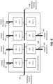
- FIG. 2 illustrates a plan view of metal layer of the substrate 102.
- the substrate 102 includes a first power plane 201, a second power plane 203, a third power plane 205, a fourth power plane 207, a fifth power plane 209 and a sixth power plane 211.
- the first power plane 201, the second power plane 203, the third power plane 205, the fourth power plane 207, the fifth power plane 209 and the sixth power plane 211 are examples of interconnects.
- Each of the power plane is configured to provide an electrical path for an integrated device (e.g., core of an integrated device).
- the first power plane 201 may be configured to be coupled to the first core 140 of the integrated device 104
- the second power plane 203 may be configured to be coupled to the second core 142 of the integrated device 104.
- Each particular power plane is configured to be electrically coupled to a particular power resource.
- a power plane may be located on any metal layer of the substrate 102.
- a power plane may be located on a metal layer of the substrate 102 that is closest to the integrated device 104.
- Each of the power planes may be configured to be electrically coupled to one or more power management integrated devices.
- each of the power planes may be configured to as an electrical path for a particular electrical current through one or more power management integrated devices.
- FIG. 2 illustrates the substrate 102 that includes a plurality of switches 107.
- the plurality of switches 107 is coupled to the first power plane 201 and the second power plane 203.
- the plurality of switches 107 is configured to allow a current traveling through the second power plane 203 to be shared with the first power plane 201. When/if a switch is off, then a current may not flow through that particular switch. When/if a switch is on, then a current may flow through that particular switch. The more switches that are turned on, the more current may flow from the second power plane 203 to the first power plane 201. Thus, the amount of power that is shared may be controlled by controlling the number of switches from the plurality of switches 107 that are turned on.
- FIG. 2 illustrates switches are coupled to the first power plane 201 (e.g., first interconnect) and the second power plane 203 (e.g., 203). However, the switches may be coupled between any of the different power planes illustrated and described in the disclosure.
- the substrate 102 may include power rails and switches may be coupled between power planes and/or power rails.
- the plurality of interconnects 122 may include the power planes (e.g., 201, 203, 205, 207, 209, 211) and/or the power rails.
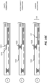
- FIG. 3 illustrates exemplary electrical paths in the package 100 with the switch 107 turned off.
- an electrical path 301 is coupled to the core 140 of the integrated device 104
- an electrical path 303 is coupled to the core 142 of the integrated device 104.
- the electrical path 301 (e.g., first electrical path) includes a first solder interconnect from the plurality of solder interconnects 130, a first plurality of interconnects from the plurality of interconnects 122 (which includes the first power plane 201 (e.g., first power interconnect)), a first solder interconnect from the plurality of solder interconnects 105 and the first core 140.
- the electrical path 303 (e.g., second electrical path) includes a second solder interconnect from the plurality of solder interconnects 130, a second plurality of interconnects from the plurality of interconnects 122 (which includes the second power plane 203 (e.g., second power interconnect)), a second solder interconnect from the plurality of solder interconnects 105 and the second core 142.
- the electrical path 303 may also include the passive device 109.
- FIG. 4 illustrates exemplary electrical paths in the package 100 with the switch 107 turned on.
- the switch 107 may be part of the electrical path 303.
- the switch 107 may be coupled to the plurality of interconnects 122.
- the switch 107 may be coupled to the integrated device 104 (e.g., configured to be electrically coupled to the core 140 of the integrated device).
- the integrated device 104 e.g., configured to be electrically coupled to the core 140 of the integrated device.
- Some power from the second power resource may travel through the second power plane 203 and the first power plane 201.
- the switch 107 is controllable by the integrated device 104 (e.g., controllable by the first core 140 and/or the second core 142).
- the switch 107 may be turned on and off by the integrated device 104. More power may be shared with the first power plane 201 and the first core 140 by turning on additional switches, which provides additional electrical paths for power to travel to the first core 140.
- FIG. 5 illustrates an electrical circuit diagram 500 for the package 100.
- the electrical circuit diagram 500 includes a first circuit 501 and a second circuit 503.
- the first circuit 501 may be an electrical representation of the electrical path 301.
- the second circuit 503 may be an electrical representation of the electrical path 303.
- the first circuit 501 is configured to be electrically coupled to the second circuit 503 through at least one switch 107.
- the first circuit 501 may include first interconnects from the board 190, a first power plane 201 and the first core 140.
- the second circuit 503 may include second interconnects from the board 190, a second power plane 203, the passive device 109, and the second core 142.
- the at least one switch 107 is part of the second circuit 503, which is located in the substrate 102.
- the at least one switch 107 may be located near the solder interconnects 130 (e.g., ball grid array).
- the at least one switch 107 may part of the substrate 102 where the passive device 109 is coupled
- FIG. 6 illustrates an example of the integrated device 104 that includes the first core 140, the second core 142, a third core 143, a fourth core 144, a fifth core 145, a sixth core 146, a seventh core 147 and an eighth core 148.
- the first core 140 is coupled to the first electrical path 301, which is coupled to a first power resource.
- the second core 142 is coupled to the second electrical path 303, which is coupled to a second power resource.
- the second power resource is a shareable power resource.
- the third core 143 is coupled to the third electrical path 603, which is coupled to a third power resource.
- the fourth core 144 is coupled to the fourth electrical path 604, which is coupled to a fourth power resource.
- the second power resource is shareable with the first core 140, the third core 143 and/or the fourth core 144.
- switches e.g., 107 may be used to allow the second power resource to be shareable with the first core 140, the third core 143 and/or the fourth core 144.
- the fifth core 145 is coupled to the fifth electrical path 605, which is coupled to a fifth power resource.
- the sixth core 146 is coupled to the sixth electrical path 606, which is coupled to a sixth power resource.
- the seventh core 147 is coupled to the seventh electrical path 607, which is coupled to a seventh power resource.
- the eighth core 148 is coupled to the eighth electrical path 608, which is coupled to an eighth power resource.
- the eighth power resource is a shareable power resource.
- the eighth power resource is shareable with the fifth core 145, the sixth core 146 and/or the seventh core 147.
- Several switches (e.g., 107) may be used to allow the eighth power resource to be shareable with the fifth core 145, the sixth core 146 and/or the seventh core 147.
- the use of sharing power resources may be applicable between memory and/or cores of an integrated device. (e.g., between two memories, between memory and core of an integrated devices).
- the use of shareable power resources may be applicable between integrated devices of a package. For example, a power resource that is allocated to be used by a first integrated device may be shared with a second integrated device.
- the integrated device e.g., 104, 740, 742 may include a die (e.g., semiconductor bare die).
- the integrated device may include a radio frequency (RF) device, a passive device, a filter, a capacitor, an inductor, an antenna, a transmitter, a receiver, a gallium arsenide (GaAs) based integrated device, a surface acoustic wave (SAW) filters, a bulk acoustic wave (BAW) filter, a light emitting diode (LED) integrated device, a silicon (Si) based integrated device, a silicon carbide (SiC) based integrated device, a memory, power management processor, and/or combinations thereof.
- An integrated device e.g., 104, 740, 742
- Exemplary Package Comprising an Integrated Devices Configured for Shareable Power Resource
- FIGS. 7 and 8 illustrate a package 700 that includes a first integrated device 740 and a second integrated device 742.
- the package 700 is similar to the package 100 of FIG. 1 and FIGS. 3-4 , and thus may include the same components and/or similar components, as the package 100.
- the first integrated device 740 may include at least one core.
- the second integrated device 742 may include at least one core.
- the first integrated device 740 and the second integrated device 742 are coupled to the substrate 102.
- the first integrated device 740 is coupled to the substrate 102 through the plurality of solder interconnects 105.
- the first integrated device 740 may be coupled to the substrate 102 through the plurality of solder interconnects 105 and pillar interconnects.
- the second integrated device 742 is coupled to the substrate 102 through the plurality of solder interconnects 705.
- the second integrated device 742 may be coupled to the substrate 102 through the plurality of solder interconnects 705 and pillar interconnects.
- FIG. 7 illustrates exemplary electrical paths in the package 700 with the switch 107 turned off.
- an electrical path 701 is coupled to the first integrated device 740
- an electrical path 703 is coupled to the second integrated device 742.
- the electrical path 701 (e.g., first electrical path) includes a first solder interconnect from the plurality of solder interconnects 130, a first plurality of interconnects from the plurality of interconnects 122 (which includes the first power plane 201 (e.g., first power interconnect)), a first solder interconnect from the plurality of solder interconnects 105 and the first integrated device 740.
- the electrical path 703 (e.g., second electrical path) includes a second solder interconnect from the plurality of solder interconnects 130, a second plurality of interconnects from the plurality of interconnects 122 (which includes the second power plane 203 (e.g., second power interconnect)), a second solder interconnect from the plurality of solder interconnects 705 and the second integrated device 742.
- the electrical path 703 may also include the passive device 109.
- FIG. 8 illustrates exemplary electrical paths in the package 700 with the switch 107 turned on.
- the switch 107 may be part of the electrical path 703.
- the switch 107 may be coupled to the plurality of interconnects 122.
- the switch 107 may be coupled to the integrated device 740 (e.g., configured to be electrically coupled to the integrated device 740 of the integrated device).
- the switch 107 is turned on, some power from the second power resource travelling through the electrical path 703 is shared and diverted to the first integrated device 740 through the switch 107.
- Some power from the second power resource may travel through the second power plane 203 and the first power plane 201.
- the switch 107 is controllable by the first integrated device 740 and/or the second integrated device 742.
- the switch 107 may be turned on and off by the first integrated device 740 and/or the second integrated device 742. More power may be shared with the first power plane 201 and the first integrated device740 by turning on additional switches, which provides additional electrical paths for power to travel to the first core 140.
- FIG. 9 illustrates an exemplary flow diagram of a method 900 for sharing power resources in a package.
- the method 900 may be implemented by one or more integrated devices.
- the method 900 may be implemented by one or more cores of an integrated devices.
- the method 900 may be implemented by the integrated device 104 of the package 100.
- the method 900 may be implemented by the integrated devices 740 and/or 742 of the package 700.
- the method operates (at 905) one or more cores (e.g., 140, 142) of an integrated device (e.g., 104).
- Operating one or more cores includes reading and executing instructions. Each core may perform separate and/or different functions. In some implementations, the cores may be part of separate integrated devices. Operating one or more cores may also include utilizing one or more memory.
- the method determines (at 910) that at least one core of an integrated device needs and/pr wants more power.
- Different implementations may have different criteria / criterion for determining whether one or more core needs and/or wants more power. For example, when the amount of power that is provided to a core is less than the maximum allowable power, the method may determine that the core needs and/or wants more power. Whether a core needs more power may mean whether a core wants more power and/or may benefit from more power. For example, a core may need and/or want more power when the core is operating at a lower frequency than the maximum frequency. In some implementations, more than one core may need and/or want more power.
- the method 900 may also determine whether there is available shareable power that is allocated for another core. It is noted that not all power that is allocated to a core is shareable to another core. In some implementations, power allocated to a particular core is shareable with another core, when the particular core is operating at less than maximum capacity and/or the particular core is not being utilized. Thus, even if one or more core may need and/or want more power, there may not be power to share from a power resource allocated to another core.
- the method turns on (at 915) at least one switch to share power resource allocated to a particular core to another core of the integrated device.
- the switch may include a transistor.
- turning on a switch may include applying a voltage to a gate interconnect of a transistor.
- the more switches that are turned on the more power is shared with another core of the integrated devices.
- the number of switches that is turned on may vary in real time. That is, the number of switches that are turned on may be different during different times of the operations of one or more cores of the integrated devices. It is noted that none of the switches may be turned on when there is no available power to share.
- the method may determine that no additional power is available to be shared from another core. In such instance, the method may not turn on a switch and/or any additional switches. As an example, the method may turn on a first switch and a second switch. The first switch and the second switch are coupled to a first power interconnect and a second power interconnect of a substrate. The first power interconnect may be coupled to a first core and the second power interconnect may be coupled to a second core. Turning on the first switch and the second switch may result in some of the second power resource to travel from the second power interconnect to the first power interconnect through the first switch and the second switch.
- turning on at least one switch includes turning on some switch and/or all switches between two different power interconnects (e.g., power planes).
- the method may turn off (at 920) at least one switch to stop sharing power resources and/or reduce the sharing of power resources.
- the switch may include a transistor.
- turning off a switch may include stopping a voltage from being applied to a gate interconnect of a transistor. Turning off a particular switch may mean that power may not flow through that particular switch. However, power may still flow between different power interconnects through another switch that is still turned on.
- the method 900 may continually and iteratively check in real time the power requirements of integrated devices and/or cores of integrated devices, and turn on and off one or more switches to provide power resources as needed to the various integrated devices and/or the various cores of integrated devices.
- the criteria / criterion for determining whether or not an integrated device e.g., core of an integrated device
- an integrated device e.g., core of an integrated device
- the criteria / criterion for determining whether or not an integrated device may vary with different implementations. Examples of what may be used to determine whether more power is needed for an integrated device is the strength of the voltage, the strength of the current of the power that is provided to the integrated devices, and/or the operating frequency of the core(s).
- the method 900 may operate an integrated device that includes a first core and a second core, where a first power resource is directed to the first core and a second power resource is directed to the second core.
- the method 900 may determine that the first core of the integrated device needs and/or wants more power.
- the method 900 may turn on at least one switch to reroute some of the second power resource to the first core of the integrated device (when there is available power from the second power resource).
- turning on at least one switch includes turning on some but not all of the switches coupled between a first power interconnect coupled to the first core and a second power interconnect coupled to the second core.
- the method 900 may further determine that the first core of the integrated device does not need more power (e.g., does not need all the power than is provided by the first power resource and some power from the second power resource). The method 900 may turn off the at least one switch to stop the rerouting of some of the second power resource to the first core of the integrated device. The method 900 may further determine that the first core of the integrated device needs further power (e.g., needs further power than what is already provided by the first power resource and some power from the second power resource). The method 900 may turn on more or all of the switches coupled between the first power interconnect coupled to the first core and the second power interconnect coupled to the second core, to reroute more of the second power resource to the first core of the integrated device.
- the method 900 may turn on more or all of the switches coupled between the first power interconnect coupled to the first core and the second power interconnect coupled to the second core, to reroute more of the second power resource to the first core of the integrated device.
- the method 900 may be applicable to cores of the same integrated device, cores of different integrated devices and/or different integrated devices.
- the method 900 may also be applicable to memories of an integrated devices (e.g., between two memories, between a memory and a core of an integrated device).
- one or more core as described above in FIG. 9 may be applicable to one memory.
- the method 900 may be applicable to two or more integrated devices.
- the method 900 may operate a first integrated device and a second integrated device, where a first power resource is directed to the first integrated device and a second power resource is directed to the second integrated device.
- the method 900 may determine that the first integrated device needs and/or wants more power.
- the method 900 may turn on at least one switch to reroute some of the second power resource to the first integrated device.
- turning on at least one switch includes turning on some but not all of the switches coupled between a first power interconnect coupled to the first integrated device and a second power interconnect coupled to the second integrated device.
- the method 900 may further determine that the first integrated device does not need more power (e.g., does not need all the power than is provided by the first power resource and some power from the second power resource).
- the method 900 may turn off the at least one switch to stop the rerouting of some of the second power resource to the first integrated device.
- the method 900 may further determine that the first integrated device needs further power (e.g., needs further power than what is already provided by the first power resource and some power from the second power resource).
- the method 900 may turn on more or all of the switches coupled between the first power interconnect coupled to the first integrated device and the second power interconnect coupled to the second integrated device, to reroute more of the second power resource to the first integrated device.
- fabricating a substrate includes several processes.
- FIGS. 10A-10C illustrate an exemplary sequence for providing or fabricating a substrate that includes a switch for sharing power resources.
- the sequence of FIGS. 10A-10C may be used to provide or fabricate the substrate 102 that includes at least one switch.
- FIGS. 10A-10C may combine one or more stages in order to simplify and/or clarify the sequence for providing or fabricating a substrate.
- the order of the processes may be changed or modified.
- one or more of processes may be replaced or substituted.
- Stage 3 illustrates a state after a gate dielectric layer 176 is formed over the interconnect 1001.
- a deposition process may be used to form the gate dielectric layer 176.
- Different implementations may use different materials for the gate dielectric layer 176.
- the gate dielectric layer 176 may include HfO 2 (hafnium oxide), SiO 2 (silicon dioxide) Al 2 O 3 (aluminum oxide) and/or combinations thereof.
- Stage 6 illustrates a state after a dielectric layer 1020 is formed over the carrier 1000, the switch 107 and the interconnects 1001.
- the dielectric layer 1020 may include polyimide. However, different implementations may use different materials for the dielectric layer 1020.
- the dielectric layer 1020 may include the dielectric layer 1002. A deposition process may be used to form the dielectric layer 1020.
- Stage 7 illustrates a state after a plurality of cavities 1011 is formed in the dielectric layer 1020.
- the plurality of cavities 1011 may be formed using an etching process or laser process.
- Stage 9 illustrates a state after another dielectric layer 1022 is formed over the dielectric layer 1020.
- a deposition process may be used to form the dielectric layer 1022.
- Stage 11 illustrates a state after interconnects 1023 are formed in and over the dielectric layer 1022.
- interconnects 1023 For example, via, pad and/or trace may be formed.
- a plating process may be used to form the interconnects.
- Stage 12 illustrates after the carrier 1000 is decoupled (e.g., removed, grinded out) from the dielectric layer 1020, leaving the substrate 102 (e.g., coreless substrate).
- the coreless substrate is an embedded trace substrate (ETS).
- Stage 11 illustrates the substrate 102 that includes the dielectric layer 1020, the dielectric layer 1022.
- the dielectric layer 1020 and the dielectric layer 1022 may be considered as one dielectric layer (e.g., single dielectric layer).
- the substrate 102 includes the plurality of interconnects 1001, the plurality of interconnects 1013, and the plurality of interconnects 1023.
- the plurality of interconnects 1001, the plurality of interconnects 1013, and the plurality of interconnects 1023 may be represented by the plurality of interconnects 122.
- Some of the interconnects from the substrate 102 may be configured as power interconnects (e.g., power planes) as described in the disclosure.
- a chemical vapor deposition (CVD) process and/or a physical vapor deposition (PVD) process for forming the metal layer(s).
- CVD chemical vapor deposition
- PVD physical vapor deposition
- a sputtering process, a spray coating process, and/or a plating process may be used to form the metal layer(s).
- sequence of FIG. 11 may combine one or more processes in order to simplify and/or clarify the method for providing or fabricating a substrate.
- order of the processes may be changed or modified.
- the method provides (at 1105) a carrier 1000.
- the method forms (at 1110) a metal layer over the carrier 1000.
- the metal layer may be patterned to form interconnects 1001.
- Some of the interconnects 1001 may define a gate interconnect 170, a source interconnect 172 and/or a drain interconnect 174.
- a plating process may be used to form the metal layer and interconnects.
- a dielectric layer may be formed after the interconnects 1001 are formed.
- Stage 1 of FIG. 10A illustrates and describes an example of providing a carrier and forming interconnects.
- the method forms (at 1115) at least one switch 107 that includes a gate dielectric layer 176 and a channel 178.
- One or more deposition process may be used to form the gate dielectric layer 176 and the channel 178.
- the gate dielectric layer 176 may include HfO 2 (hafnium oxide), SiO 2 (silicon dioxide) Al 2 O 3 (aluminum oxide) and/or combinations thereof.
- the channel 178 may include polycrystalline SiGe (silicon germanium), CdSe (Cadmium selenide), IgZo (indium gallium zinc oxide), tungsten (W)-Doped In 2 O 3 (indium oxide) and/or combinations thereof.
- the source interconnect 172 and/or the drain interconnect 174 may be doped.
- the switch may include a transistor. Stages 3-5 of FIG. 10A illustrate and describe an example of forming a channel and a gate dielectric layer.
- the method forms (at 1120) a dielectric layer 1020 over the carrier 1000, the interconnects 1001 and the switch 107.
- the dielectric layer 1020 may include polyimide.
- Forming the dielectric layer may also include forming a plurality of cavities (e.g., 1011) in the dielectric layer 1020.
- the plurality of cavities may be formed using an etching process or laser process.
- Stage 56of FIG. 10A and stage 7 of FIG. 10B illustrates and describes an example of forming a dielectric layer and cavities.
- the method forms (at 1125) interconnects in and over the dielectric layer.
- the interconnects 1113 may formed.
- a plating process may be used to form the interconnects.
- Forming interconnects may include providing a patterned metal layer over and/or in the dielectric layer.
- Stage 8 of FIG. 10B illustrates and describes an example of forming an interconnect.
- the method forms (at 1130) a dielectric layer 1022 over the dielectric layer 1020 and the interconnects 1113.
- the dielectric layer 1022 may include polyimide.
- Forming the dielectric layer may also include forming a plurality of cavities (e.g., 1021) in the dielectric layer 1022.
- the plurality of cavities may be formed using an etching process or laser process.
- Stage 9 of FIG. 10B and stage 10 of FIG. 10C illustrate and describe examples of forming a dielectric layer and a cavity.
- the method forms (at 1135) interconnects in and/or over the dielectric layer.
- the interconnects 1023 may be formed.
- a plating process may be used to form the interconnects.
- Forming interconnects may include providing a patterned metal layer over an in the dielectric layer.
- Stage 11 of FIG. 10C illustrates and describes examples of forming interconnects
- the method may form additional dielectric layer(s) and additional interconnects as described at 1130 and 1135.
- the method may decouple (e.g., remove, grind out) the carrier (e.g., 1100) from the dielectric layer 1020, leaving the substrate.
- the coreless substrate is an embedded trace substrate (ETS).
- ETS embedded trace substrate
- a chemical vapor deposition (CVD) process and/or a physical vapor deposition (PVD) process for forming the metal layer(s).
- CVD chemical vapor deposition
- PVD physical vapor deposition
- a sputtering process, a spray coating process, and/or a plating process may be used to form the metal layer(s).
- FIG. 12 illustrates various electronic devices that may be integrated with any of the aforementioned device, integrated device, integrated circuit (IC) package, integrated circuit (IC) device, semiconductor device, integrated circuit, die, interposer, package, package-on-package (PoP), System in Package (SiP), or System on Chip (SoC).
- a mobile phone device 1202, a laptop computer device 1204, a fixed location terminal device 1206, a wearable device 1208, or automotive vehicle 1210 may include a device 1200 as described herein.
- the device 1200 may be, for example, any of the devices and/or integrated circuit (IC) packages described herein.
- the devices 1202, 1204, 1206 and 1208 and the vehicle 1210 illustrated in FIG. 12 are merely exemplary.
- Other electronic devices may also feature the device 1200 including, but not limited to, a group of devices (e.g., electronic devices) that includes mobile devices, hand-held personal communication systems (PCS) units, portable data units such as personal digital assistants, global positioning system (GPS) enabled devices, navigation devices, set top boxes, music players, video players, entertainment units, fixed location data units such as meter reading equipment, communications devices, smartphones, tablet computers, computers, wearable devices (e.g., watches, glasses), Internet of things (IoT) devices, servers, routers, electronic devices implemented in automotive vehicles (e.g., autonomous vehicles), or any other device that stores or retrieves data or computer instructions, or any combination thereof.
- a group of devices e.g., electronic devices
- devices that includes mobile devices, hand-held personal communication systems (PCS) units, portable data units such as personal digital assistants, global positioning system (GPS) enabled devices, navigation devices, set top boxes, music players, video players, entertainment units, fixed location data units such as meter reading equipment, communications devices, smartphones,
- FIGS. 1-9 , 10A-10C , and/or 11-12 may be rearranged and/or combined into a single component, process, feature or function or embodied in several components, processes, or functions. Additional elements, components, processes, and/or functions may also be added without departing from the disclosure. It should also be noted FIGS. 1-9 , 10A-10C , and/or 11-12 and its corresponding description in the present disclosure is not limited to dies and/or ICs. In some implementations, FIGS. 1-9 , 10A-10C , and/or 11-12 and its corresponding description may be used to manufacture, create, provide, and/or produce devices and/or integrated devices.
- a device may include a die, an integrated device, an integrated passive device (IPD), a die package, an integrated circuit (IC) device, a device package, an integrated circuit (IC) package, a wafer, a semiconductor device, a package-on-package (PoP) device, a heat dissipating device and/or an interposer.
- IPD integrated passive device
- IC integrated circuit
- IC integrated circuit
- IC integrated circuit
- wafer a semiconductor device
- PoP package-on-package
- the figures in the disclosure may represent actual representations and/or conceptual representations of various parts, components, objects, devices, packages, integrated devices, integrated circuits, and/or transistors.
- the figures may not be to scale. In some instances, for purpose of clarity, not all components and/or parts may be shown. In some instances, the position, the location, the sizes, and/or the shapes of various parts and/or components in the figures may be exemplary. In some implementations, various components and/or parts in the figures may be optional.
- One or more processors in the processing system may execute software.
- Software shall be construed broadly to mean instructions, instruction sets, code, code segments, program code, programs, subprograms, software modules, applications, software applications, software packages, routines, subroutines, objects, executables, threads of execution, procedures, functions, etc., whether referred to as software, firmware, middleware, microcode, hardware description language, or otherwise.
- the software may reside on a computer-readable medium.
- the computer-readable medium may be a non-transitory computer-readable medium.
- a non-transitory computer-readable medium includes, by way of example, a magnetic storage device (e.g., hard disk, floppy disk, magnetic strip), an optical disk (e.g., a compact disc (CD) or a digital versatile disc (DVD)), a smart card, a flash memory device (e.g., a card, a stick, or a key drive), a random access memory (RAM), a read only memory (ROM), a programmable ROM (PROM), an erasable PROM (EPROM), an electrically erasable PROM (EEPROM), a register, a removable disk, and any other suitable medium for storing software and/or instructions that may be accessed and read by a computer.
- a magnetic storage device e.g., hard disk, floppy disk, magnetic strip
- an optical disk e.g., a compact disc (CD) or a digital versatile disc (DVD)
- the computer-readable medium may reside in a processing system, external to the processing system, or distributed across multiple entities including the processing system.
- the computer-readable medium may be embodied in a computer program product.
- the computer-readable medium may be part of a memory.
- a computer program product may include a computer-readable medium in packaging materials.
- Coupled is used herein to refer to the direct or indirect coupling (e.g., mechanical coupling) between two objects. For example, if object A physically touches object B, and object B touches object C, then objects A and C may still be considered coupled to one another-even if they do not directly physically touch each other.
- a component that is located on top may be located over a component that is located on a bottom.
- a top component may be considered a bottom component, and vice versa.
- a first component that is located "over" a second component may mean that the first component is located above or below the second component, depending on how a bottom or top is arbitrarily defined.
- a first component may be located over (e.g., above) a first surface of the second component, and a third component may be located over (e.g., below) a second surface of the second component, where the second surface is opposite to the first surface.
- an interconnect is an element or component of a device or package that allows or facilitates an electrical connection between two points, elements and/or components.
- an interconnect may include a trace, a via, a pad, a pillar, a metallization layer, a redistribution layer, and/or an under bump metallization (UBM) layer / interconnect.
- an interconnect may include an electrically conductive material that may be configured to provide an electrical path for a signal (e.g., a data signal), ground and/or power.
- An interconnect may include more than one element or component.
- An interconnect may be defined by one or more interconnects.
- An interconnect may include one or more metal layers.
- An interconnect may be part of a circuit.
- a chemical vapor deposition (CVD) process may be used to form the interconnects.
- PVD physical vapor deposition
- a sputtering process may be used to form the interconnects.
- a spray coating may be used to form the interconnects.
- a package comprising an integrated device and a substrate coupled to the integrated device.
- the integrated device includes a first core and a second core.
- the substrate includes a first power interconnect configured to provide a first electrical path for a first power resource to the first core of the integrated device; a second power interconnect configured to provide a second electrical path for a second power resource to the second core of the integrated device; and a switch coupled to the first power interconnect and the second power interconnect, wherein if the switch is turned on, the switch is configured to enable at least some of the power resource from the second power resource to contribute to the first core of the integrated device.
- Aspect 2 The package of aspect 1, wherein if the switch is turned off, the switch is configured such that the power from the second power resource does not contribute to the first core through the switch.
- Aspect 3 The package of aspects 1 through 2, wherein the switch includes at least one transistor.
- Aspect 4 The package of aspect 3, wherein the at least one transistor comprises a source interconnect, a drain interconnect, a channel, and a gate interconnect.
- Aspect 5 The package of aspects 1 through 4, wherein the first power interconnect includes a first power plane, and wherein the second power interconnect includes a second power plane.
- Aspect 7 The package of aspects 1 through 6, wherein the switch is configured to be controlled by the integrated device.
- Aspect 8 The package of aspects 1 through 7, further comprising a second switch coupled to the first power interconnect and the second power interconnect, wherein if the second switch is turned on, the second switch is configured to enable at least some of the power resource from the second power resource to contribute to the first core of the integrated device.
- Aspect 9 The package of aspects 1 through 7, wherein the integrated device further comprises a third core, wherein the substrate further comprises: a third power interconnect configured to provide a third electrical path for a third power resource to the third core of the integrated device; and a second switch coupled to the third power interconnect and the second power interconnect, wherein if the second switch is turned on, the second switch is configured to enable at least some of the power resource from the second power resource to contribute to the third core of the integrated device.
- Aspect 10 The package of aspects 1 through 9, wherein the first power resource and the second power resource are part of a power grid resource that is configured to be coupled to one or more power management integrated devices.
- Aspect 13 The package of aspect 12, wherein the integrated device is further configured to: determine whether the first core of the integrated device does not need more power; and if it is determined that the first core does not need more power, turn off the switch to stop the rerouting of some of the second power resource to the first core of the integrated device through the switch.
- Aspect 21 The package of aspects 15 through 19, wherein the first power resource includes a first electrical current from a power management integrated device, and wherein the second power resource includes a second electrical current from the power management integrated device.
- Aspect 27 The method of aspect 26, further comprising: determining that the first core of the integrated device does not need more power; and turning off the at least one switch to stop the rerouting of some of the second power resource to the first core of the integrated device through the at least one switch.
- Aspect 28 The method of aspects 26 through 27, wherein turning on at least one switch includes turning on some but not all of the switches coupled between a first power interconnect coupled to the first core and a second power interconnect coupled to the second core.
- Aspect 29 The method of aspect 28, further comprising: determining that the first core of the integrated device needs further power; and turning on all of the switches coupled between the first power interconnect coupled to the first core and the second power interconnect coupled to the second core, to reroute more of the second power resource to the first core of the integrated device through the at least one switch.
- Aspect 30 The method of aspects 26 through 29, wherein the first power resource and the second power resource travel through a power management integrated device.
- a method comprising: operating a first integrated device, wherein a first power resource is directed to the first integrated device; operating a second integrated device, wherein a second power resource is directed to the second integrated device; determining that the first integrated device needs more power; and turning on at least one switch to reroute some of the second power resource to the first integrated device through the at least one switch.
- Aspect 32 The method of aspect 31, further comprising: determining that the first integrated device does not need more power; and turning off the at least one switch to stop the rerouting of some of the second power resource to the first integrated device through the at least one switch.
- Aspect 33 The method of aspects 31 through 32, wherein turning on at least one switch includes turning on some but not all of the switches coupled between a first power interconnect coupled to the first integrated device and a second power interconnect coupled to the second integrated device.
- Aspect 34 The method of aspect 33, further comprising: determining that the first integrated device needs further power; and turning on all of the switches coupled between the first power interconnect coupled to the first integrated device and the second power interconnect coupled to the second integrated device, to reroute more of the second power resource to the first integrated device through the at least one switch.
- Aspect 35 The method of aspects 31 through 34, wherein the first power resource and the second power resource travel through a power management integrated device.
Landscapes
- Semiconductor Integrated Circuits (AREA)
- Structure Of Printed Boards (AREA)
Claims (15)
- Ein Package (100), aufweisend:ein integriertes Bauelement (104), das aufweist:einen ersten Kern (140), undeinen zweiten Kern (142), undein Substrat (102), das mit dem integrierten Bauelement (104) gekoppelt ist, wobei das Substrat (102) aufweist:eine erste Leistungsverbindung, die konfiguriert ist zum Vorsehen eines ersten elektrischen Pfads (301) für eine erste Leistungsressource zu dem ersten Kern (140) des integrierten Bauelements (102),eine zweite Leistungsverbindung, die konfiguriert ist zum Vorsehen eines zweiten elektrischen Pfads (303) für eine zweite Leistungsressource zu dem zweiten Kern (142) des integrierten Bauelements (102), undeinen Schalter (107), der mit der ersten Leistungsverbindung und der zweiten Leistungsverbindung gekoppelt ist, wobei, wenn der Schalter (107) eingeschaltet ist, der Schalter (107) konfiguriert ist, um zu ermöglichen, dass wenigstens ein Teil der Leistungsressource von der zweiten Leistungsressource zu dem ersten Kern (140) des integrierten Bauelements (104) beiträgt.
- Package (100) nach Anspruch 1, wobei, wenn der Schalter (107) ausgeschaltet ist, der Schalter derart konfiguriert ist, dass die Leistung von der zweiten Leistungsressource nicht zu dem ersten Kern (140) durch den Schalter (107) beiträgt.
- Package (100) nach Anspruch 1,wobei die erste Leistungsverbindung eine erste Leistungsebene umfasst, undwobei die zweite Leistungsverbindung eine zweite Leistungsebene umfasst, wobei die erste Leistungsebene und die zweite Leistungsebene auf der gleichen Metallschicht des Substrats angeordnet sind.
- Package (100) nach Anspruch 1, wobei der Schalter konfiguriert ist, um durch das integrierte Bauelement (104) gesteuert zu werden.
- Package (100) nach Anspruch 1, die weiterhin einen zweiten Schalter umfasst, der mit der ersten Leistungsverbindung und der zweiten Leistungsverbindung gekoppelt ist, wobei, wenn der zweite Schalter eingeschaltet ist, der zweite Schalter konfiguriert ist, um zu ermöglichen, dass wenigstens ein Teil der Leistungsressource von der zweiten Leistungsressource zu dem ersten Kern der integrierten Schaltung beiträgt.
- Package (100) nach Anspruch 1, wobei die erste Leistungsressource und die zweite Leistungsressource Teil einer Stromnetzressource sind, die konfiguriert ist, um mit einem oder mehreren integrierten Leistungsverwaltungselementen gekoppelt zu werden.
- Package (100) nach Anspruch 1,wobei die erste Leistungsressource einen ersten elektrischen Strom von einem integrierten Leistungsverwaltungselement enthält, undwobei die zweite Leistungsressource einen zweiten elektrischen Strom von dem integrierten Leistungsverwaltungselement enthält.
- Package (100) nach Anspruch 1, wobei das integrierte Bauelement (104) konfiguriert ist zum:Bestimmen, ob der erste Kern (140) des integrierten Bauelements mehr Leistung benötigt, undwenn bestimmt wird, dass der erste Kern (140) mehr Leistung benötigt, Einschalten des Schalters (107) für das Umlenken eines Teils der zweiten Leistungsressource zu dem ersten Kern (140) des integrierten Bauelements,wobei das integrierte Bauelement weiterhin konfiguriert ist zum:Bestimmen, ob der erste Kern (140) des integrierten Bauelements nicht mehr Leistung benötigt, undwenn bestimmt wird, dass der erste Kern nicht mehr Leistung benötigt, Ausschalten des Schalters (107) für das Stoppen des Umlenkens eines Teils der zweiten Leistungsressource zu dem ersten Kern des integrierten Bauelements durch den Schalter.
- Package (100) nach Anspruch 8, wobei das integrierte Bauelement (104) weiterhin konfiguriert ist zum:Bestimmen, ob der erste Kern des integrierten Bauelements weiterhin Leistung benötigt, undwenn bestimmt wird, dass der erste Kern weiterhin Leistung benötigt, Einschalten eines zweiten Schalters, der zwischen der mit dem ersten Kern gekoppelten ersten Leistungsverbindung und der mit dem zweiten Kern gekoppelten zweiten Leistungsverbindung gekoppelt ist, um mehr der zweiten Leistungsressource zu dem ersten Kern des integrierten Bauelements umzulenken.
- Ein Package (700), aufweisend:ein erstes integriertes Bauelement (740),ein zweites integriertes Bauelement (742), undein Substrat (102), das mit dem ersten integrierten Bauelement (740) und dem zweiten integrierten Bauelement (742) gekoppelt ist, wobei das Substrat (102) aufweist:eine erste Leistungsverbindung, die konfiguriert ist zum Vorsehen eines ersten elektrischen Pfads (701) für eine erste Leistungsressource zu dem ersten integrierten Bauelement (740),eine zweite Leistungsverbindung, die konfiguriert ist zum Vorsehen eines zweiten elektrischen Pfads (703) für eine zweite Leistungsressource zu dem zweiten integrierten Bauelement (742), undeinen Schalter (107), der mit der ersten Leistungsverbindung und der zweiten Leistungsverbindung gekoppelt ist, wobei, wenn der Schalter (107) eingeschaltet ist, der Schalter (107) konfiguriert ist, um zu ermöglichen, dass wenigstens ein Teil der Leistungsressource von der zweiten Leistungsressource zu dem ersten integrierten Bauelement (740) beiträgt.
- Package (700) nach Anspruch 10, wobei, wenn der Schalter (107) ausgeschaltet ist, der Schalter (107) derart konfiguriert ist, dass die Leistung von der zweiten Leistungsressource nicht zu der ersten integrierten Schaltung durch den Schalter (107) beiträgt.
- Package (700) nach Anspruch 10, wobei der Schalter (107) konfiguriert ist, um durch das erste integrierte Bauelement (740) und/oder das zweite integrierte Bauelement (742) gesteuert zu werden.
- Package (700) nach Anspruch 10, wobei das erste integrierte Bauelement (740) konfiguriert ist zum:Bestimmen, ob das erste integrierte Bauelement (740) mehr Leistung benötigt, undwenn bestimmt wird, dass das erste integrierte Bauelement (740) mehr Leistung benötigt, Einschalten des Schalters (107) für das Umlenken eines Teils der zweiten Leistungsressource zu dem ersten integrierten Bauelement,wobei das erste integrierte Bauelement (740) weiterhin konfiguriert ist zum:Bestimmen, ob das erste integrierte Bauelement nicht mehr Leistung benötigt, undwenn bestimmt wird, dass das erste integrierte Bauelement nicht mehr Leistung benötigt, Ausschalten des Schalters für das Stoppen des Umlenkens eines Teils der zweiten Leistungsressource zu dem ersten integrierten Bauelement durch den Schalter,wobei das erste integrierte Bauelement (740) weiterhin konfiguriert ist zum:Bestimmen, ob das erste integrierte Bauelement weiterhin Leistung benötigt, undwenn bestimmt wird, dass das erste integrierte Bauelement weiterhin Leistung benötigt, Einschalten eines zweiten Schalters, der zwischen der mit dem ersten integrierten Bauelement gekoppelten ersten Leistungsverbindung und der mit dem zweiten integrierten Bauelement gekoppelten zweiten Leistungsverbindung gekoppelt ist, um mehr der zweiten Leistungsressource zu dem ersten integrierten Bauelement umzulenken.
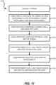
- Ein Verfahren, aufweisend:Betreiben (905) eines integrierten Bauelements, die einen ersten Kern und einen zweiten Kern enthält, wobei eine erste Leistungsressource zu dem ersten Kern gerichtet wird und eine zweite Leistungsressource zu dem zweiten Kern gerichtet wird,Bestimmen (910), dass der erste Kern des integrierten Bauelements mehr Leistung benötigt, undEinschalten (915) wenigstens eines Schalters für das Umlenken eines Teils der zweiten Leistungsressource zu dem ersten Kern des integrierten Bauelements.
- Ein Verfahren, aufweisend:Betreiben (905) eines ersten integrierten Bauelements, wobei eine erste Leistungsressource zu dem ersten integrierten Bauelement gerichtet wird,Betreiben (905) eines zweiten integrierten Bauelements, wobei eine zweite Leistungsressource zu dem zweiten integrierten Bauelement gerichtet wird,Bestimmen (910), dass das erste integrierte Bauelement mehr Leistung benötigt, undEinschalten (915) wenigstens eines Schalters für das Umlenken wenigstens eines Teils der zweiten Leistungsressource zu dem ersten integrierten Bauelement.
Applications Claiming Priority (2)
| Application Number | Priority Date | Filing Date | Title |
|---|---|---|---|
| US17/162,621 US11764186B2 (en) | 2021-01-29 | 2021-01-29 | Package comprising an integrated device configured for shareable power resource |
| PCT/US2021/063630 WO2022164527A1 (en) | 2021-01-29 | 2021-12-15 | Package comprising an integrated device configured for shareable power resource |
Publications (3)
| Publication Number | Publication Date |
|---|---|
| EP4285410A1 EP4285410A1 (de) | 2023-12-06 |
| EP4285410C0 EP4285410C0 (de) | 2025-04-30 |
| EP4285410B1 true EP4285410B1 (de) | 2025-04-30 |
Family
ID=80445787
Family Applications (1)
| Application Number | Title | Priority Date | Filing Date |
|---|---|---|---|
| EP21854901.2A Active EP4285410B1 (de) | 2021-01-29 | 2021-12-15 | Verpackung mit einer integrierten vorrichtung, die für gemeinsam nutzbare leistungsressourcen konfiguriert ist |
Country Status (7)
| Country | Link |
|---|---|
| US (2) | US11764186B2 (de) |
| EP (1) | EP4285410B1 (de) |
| JP (1) | JP7713526B2 (de) |
| KR (1) | KR20230137325A (de) |
| CN (1) | CN116711075A (de) |
| BR (1) | BR112023014301A2 (de) |
| WO (1) | WO2022164527A1 (de) |
Families Citing this family (2)
| Publication number | Priority date | Publication date | Assignee | Title |
|---|---|---|---|---|
| US11764186B2 (en) | 2021-01-29 | 2023-09-19 | Qualcomm Incorporated | Package comprising an integrated device configured for shareable power resource |
| US11978697B2 (en) * | 2021-07-16 | 2024-05-07 | Taiwan Semiconductor Manufacturing Company, Ltd. | Package structure |
Citations (1)
| Publication number | Priority date | Publication date | Assignee | Title |
|---|---|---|---|---|
| US9935052B1 (en) * | 2014-11-26 | 2018-04-03 | Altera Corporation | Power line layout in integrated circuits |
Family Cites Families (11)
| Publication number | Priority date | Publication date | Assignee | Title |
|---|---|---|---|---|
| WO2012031362A1 (en) | 2010-09-07 | 2012-03-15 | Corporation De L ' Ecole Polytechnique De Montreal | Methods, apparatus and system to support large-scale micro- systems including embedded and distributed power supply, thermal regulation, multi-distributed-sensors and electrical signal propagation |
| US9064715B2 (en) | 2010-12-09 | 2015-06-23 | Taiwan Semiconductor Manufacturing Company, Ltd. | Networking packages based on interposers |
| US9633872B2 (en) * | 2013-01-29 | 2017-04-25 | Altera Corporation | Integrated circuit package with active interposer |
| JP2016539504A (ja) | 2013-11-21 | 2016-12-15 | ツェットエフ、フリードリッヒスハーフェン、アクチエンゲゼルシャフトZf Friedrichshafen Ag | 多機能型高電流用回路基板 |
| KR102252643B1 (ko) * | 2014-10-20 | 2021-05-17 | 삼성전자주식회사 | 시스템 온 칩의 전원 경로 제어기 |
| US9287208B1 (en) | 2014-10-27 | 2016-03-15 | Intel Corporation | Architecture for on-die interconnect |
| US10224310B2 (en) | 2015-10-29 | 2019-03-05 | Qualcomm Incorporated | Hybrid three-dimensional integrated circuit reconfigurable thermal aware and dynamic power gating interconnect architecture |
| US10664035B2 (en) | 2017-08-31 | 2020-05-26 | Qualcomm Incorporated | Reconfigurable power delivery networks |
| CN110998835A (zh) | 2017-09-13 | 2020-04-10 | 英特尔公司 | 有源硅桥 |
| US10826492B2 (en) | 2018-08-31 | 2020-11-03 | Xilinx, Inc. | Power gating in stacked die structures |
| US11764186B2 (en) | 2021-01-29 | 2023-09-19 | Qualcomm Incorporated | Package comprising an integrated device configured for shareable power resource |
-
2021
- 2021-01-29 US US17/162,621 patent/US11764186B2/en active Active
- 2021-12-15 JP JP2023544408A patent/JP7713526B2/ja active Active
- 2021-12-15 CN CN202180091319.8A patent/CN116711075A/zh active Pending
- 2021-12-15 BR BR112023014301A patent/BR112023014301A2/pt unknown
- 2021-12-15 EP EP21854901.2A patent/EP4285410B1/de active Active
- 2021-12-15 WO PCT/US2021/063630 patent/WO2022164527A1/en not_active Ceased
- 2021-12-15 KR KR1020237025096A patent/KR20230137325A/ko active Pending
-
2023
- 2023-08-03 US US18/365,063 patent/US12057436B2/en active Active
Patent Citations (1)
| Publication number | Priority date | Publication date | Assignee | Title |
|---|---|---|---|---|
| US9935052B1 (en) * | 2014-11-26 | 2018-04-03 | Altera Corporation | Power line layout in integrated circuits |
Also Published As
| Publication number | Publication date |
|---|---|
| US12057436B2 (en) | 2024-08-06 |
| EP4285410A1 (de) | 2023-12-06 |
| CN116711075A (zh) | 2023-09-05 |
| BR112023014301A2 (pt) | 2023-12-12 |
| KR20230137325A (ko) | 2023-10-04 |
| US20230387077A1 (en) | 2023-11-30 |
| JP2024505471A (ja) | 2024-02-06 |
| US20220246580A1 (en) | 2022-08-04 |
| US11764186B2 (en) | 2023-09-19 |
| EP4285410C0 (de) | 2025-04-30 |
| WO2022164527A1 (en) | 2022-08-04 |
| JP7713526B2 (ja) | 2025-07-25 |
| TW202247369A (zh) | 2022-12-01 |
Similar Documents
| Publication | Publication Date | Title |
|---|---|---|
| US11502049B2 (en) | Package comprising multi-level vertically stacked redistribution portions | |
| US12057436B2 (en) | Package comprising an integrated device configured for shareable power resource | |
| US20220246496A1 (en) | Package having a substrate comprising surface interconnects aligned with a surface of the substrate | |
| US11823983B2 (en) | Package with a substrate comprising pad-on-pad interconnects | |
| WO2017127463A1 (en) | Integrated device package comprising a tunable inductor | |
| EP4591355A1 (de) | Verpackung und vorrichtung mit einer verpackung | |
| US12142561B2 (en) | Integrated device and integrated passive device comprising magnetic material | |
| US20150279774A1 (en) | Space transformer | |
| US20210210452A1 (en) | Integrated passive device (ipd) coupled to front side of integrated device | |
| WO2024064470A1 (en) | Package comprising a flexible substrate | |
| EP4573596A1 (de) | Verpackung mit einem ersten substrat, einem zweiten substrat und einer an eine unterseite des zweiten substrats gekoppelten elektrischen vorrichtung | |
| TWI918803B (zh) | 用於將功率路由至集成裝置的封裝與方法 | |
| EP4406376A1 (de) | Elektronische vorrichtung mit einer elektrobenetzungsvorrichtung | |
| US20250006631A1 (en) | Integrated inductor including magnetic layer | |
| US20250037923A1 (en) | Package comprising a substrate with inductors and a magnetic layer | |
| US12230604B2 (en) | Package comprising stacked integrated devices with overhang | |
| US20250201786A1 (en) | Package comprising integrated devices and a passive device | |
| US20240355781A1 (en) | Integrated device comprising an offset interconnect | |
| US20250096091A1 (en) | Package comprising a substrate with via interconnect with vertical walls | |
| US20250096207A1 (en) | Package comprising a bridge located between metallization portions | |
| US20240105568A1 (en) | Package comprising a substrate with interconnects | |
| WO2025198843A1 (en) | Integrated device comprising extended metallization region for pillar interconnects | |
| WO2026080017A1 (en) | Device comprising an acoustic layer and via interconnect | |
| WO2024030719A1 (en) | Package comprising an integrated device and a first metallization portion coupled to a second metallization portion |
Legal Events
| Date | Code | Title | Description |
|---|---|---|---|
| STAA | Information on the status of an ep patent application or granted ep patent |
Free format text: STATUS: UNKNOWN |
|
| STAA | Information on the status of an ep patent application or granted ep patent |
Free format text: STATUS: THE INTERNATIONAL PUBLICATION HAS BEEN MADE |
|
| PUAI | Public reference made under article 153(3) epc to a published international application that has entered the european phase |
Free format text: ORIGINAL CODE: 0009012 |
|
| STAA | Information on the status of an ep patent application or granted ep patent |
Free format text: STATUS: REQUEST FOR EXAMINATION WAS MADE |
|
| 17P | Request for examination filed |
Effective date: 20230509 |
|
| AK | Designated contracting states |
Kind code of ref document: A1 Designated state(s): AL AT BE BG CH CY CZ DE DK EE ES FI FR GB GR HR HU IE IS IT LI LT LU LV MC MK MT NL NO PL PT RO RS SE SI SK SM TR |
|
| DAV | Request for validation of the european patent (deleted) | ||
| DAX | Request for extension of the european patent (deleted) | ||
| GRAP | Despatch of communication of intention to grant a patent |
Free format text: ORIGINAL CODE: EPIDOSNIGR1 |
|
| STAA | Information on the status of an ep patent application or granted ep patent |
Free format text: STATUS: GRANT OF PATENT IS INTENDED |
|
| INTG | Intention to grant announced |
Effective date: 20241220 |
|
| GRAS | Grant fee paid |
Free format text: ORIGINAL CODE: EPIDOSNIGR3 |
|
| GRAA | (expected) grant |
Free format text: ORIGINAL CODE: 0009210 |
|
| STAA | Information on the status of an ep patent application or granted ep patent |
Free format text: STATUS: THE PATENT HAS BEEN GRANTED |
|
| AK | Designated contracting states |
Kind code of ref document: B1 Designated state(s): AL AT BE BG CH CY CZ DE DK EE ES FI FR GB GR HR HU IE IS IT LI LT LU LV MC MK MT NL NO PL PT RO RS SE SI SK SM TR |
|
| REG | Reference to a national code |
Ref country code: CH Ref legal event code: EP Ref country code: GB Ref legal event code: FG4D |
|
| REG | Reference to a national code |
Ref country code: IE Ref legal event code: FG4D |
|
| REG | Reference to a national code |
Ref country code: DE Ref legal event code: R096 Ref document number: 602021030154 Country of ref document: DE |
|
| U01 | Request for unitary effect filed |
Effective date: 20250519 |
|
| U07 | Unitary effect registered |
Designated state(s): AT BE BG DE DK EE FI FR IT LT LU LV MT NL PT RO SE SI Effective date: 20250523 |
|
| PG25 | Lapsed in a contracting state [announced via postgrant information from national office to epo] |
Ref country code: ES Free format text: LAPSE BECAUSE OF FAILURE TO SUBMIT A TRANSLATION OF THE DESCRIPTION OR TO PAY THE FEE WITHIN THE PRESCRIBED TIME-LIMIT Effective date: 20250430 |
|
| PG25 | Lapsed in a contracting state [announced via postgrant information from national office to epo] |
Ref country code: NO Free format text: LAPSE BECAUSE OF FAILURE TO SUBMIT A TRANSLATION OF THE DESCRIPTION OR TO PAY THE FEE WITHIN THE PRESCRIBED TIME-LIMIT Effective date: 20250730 Ref country code: GR Free format text: LAPSE BECAUSE OF FAILURE TO SUBMIT A TRANSLATION OF THE DESCRIPTION OR TO PAY THE FEE WITHIN THE PRESCRIBED TIME-LIMIT Effective date: 20250731 |
|
| PG25 | Lapsed in a contracting state [announced via postgrant information from national office to epo] |
Ref country code: PL Free format text: LAPSE BECAUSE OF FAILURE TO SUBMIT A TRANSLATION OF THE DESCRIPTION OR TO PAY THE FEE WITHIN THE PRESCRIBED TIME-LIMIT Effective date: 20250430 |
|
| PG25 | Lapsed in a contracting state [announced via postgrant information from national office to epo] |
Ref country code: HR Free format text: LAPSE BECAUSE OF FAILURE TO SUBMIT A TRANSLATION OF THE DESCRIPTION OR TO PAY THE FEE WITHIN THE PRESCRIBED TIME-LIMIT Effective date: 20250430 |
|
| PG25 | Lapsed in a contracting state [announced via postgrant information from national office to epo] |
Ref country code: RS Free format text: LAPSE BECAUSE OF FAILURE TO SUBMIT A TRANSLATION OF THE DESCRIPTION OR TO PAY THE FEE WITHIN THE PRESCRIBED TIME-LIMIT Effective date: 20250731 |
|
| PG25 | Lapsed in a contracting state [announced via postgrant information from national office to epo] |
Ref country code: IS Free format text: LAPSE BECAUSE OF FAILURE TO SUBMIT A TRANSLATION OF THE DESCRIPTION OR TO PAY THE FEE WITHIN THE PRESCRIBED TIME-LIMIT Effective date: 20250830 |
|
| U20 | Renewal fee for the european patent with unitary effect paid |
Year of fee payment: 5 Effective date: 20251112 |
|
| PGFP | Annual fee paid to national office [announced via postgrant information from national office to epo] |
Ref country code: GB Payment date: 20251113 Year of fee payment: 5 |
|
| PG25 | Lapsed in a contracting state [announced via postgrant information from national office to epo] |
Ref country code: SM Free format text: LAPSE BECAUSE OF FAILURE TO SUBMIT A TRANSLATION OF THE DESCRIPTION OR TO PAY THE FEE WITHIN THE PRESCRIBED TIME-LIMIT Effective date: 20250430 |
|
| PG25 | Lapsed in a contracting state [announced via postgrant information from national office to epo] |
Ref country code: CZ Free format text: LAPSE BECAUSE OF FAILURE TO SUBMIT A TRANSLATION OF THE DESCRIPTION OR TO PAY THE FEE WITHIN THE PRESCRIBED TIME-LIMIT Effective date: 20250430 |
|
| PGFP | Annual fee paid to national office [announced via postgrant information from national office to epo] |
Ref country code: IE Payment date: 20251111 Year of fee payment: 5 |
|
| PG25 | Lapsed in a contracting state [announced via postgrant information from national office to epo] |
Ref country code: SK Free format text: LAPSE BECAUSE OF FAILURE TO SUBMIT A TRANSLATION OF THE DESCRIPTION OR TO PAY THE FEE WITHIN THE PRESCRIBED TIME-LIMIT Effective date: 20250430 |
|
| PLBE | No opposition filed within time limit |
Free format text: ORIGINAL CODE: 0009261 |
|
| STAA | Information on the status of an ep patent application or granted ep patent |
Free format text: STATUS: NO OPPOSITION FILED WITHIN TIME LIMIT |
|
| REG | Reference to a national code |
Ref country code: CH Ref legal event code: L10 Free format text: ST27 STATUS EVENT CODE: U-0-0-L10-L00 (AS PROVIDED BY THE NATIONAL OFFICE) Effective date: 20260311 |
|
| 26N | No opposition filed |
Effective date: 20260202 |