EP4283829A1 - Wireless power reception device having detune circuit - Google Patents
Wireless power reception device having detune circuit Download PDFInfo
- Publication number
- EP4283829A1 EP4283829A1 EP22798976.1A EP22798976A EP4283829A1 EP 4283829 A1 EP4283829 A1 EP 4283829A1 EP 22798976 A EP22798976 A EP 22798976A EP 4283829 A1 EP4283829 A1 EP 4283829A1
- Authority
- EP
- European Patent Office
- Prior art keywords
- circuit
- switch
- detuning
- wireless power
- voltage
- Prior art date
- Legal status (The legal status is an assumption and is not a legal conclusion. Google has not performed a legal analysis and makes no representation as to the accuracy of the status listed.)
- Pending
Links
Images





Classifications
-
- H—ELECTRICITY
- H02—GENERATION; CONVERSION OR DISTRIBUTION OF ELECTRIC POWER
- H02J—ELECTRIC POWER NETWORKS; CIRCUIT ARRANGEMENTS OR SYSTEMS FOR SUPPLYING OR DISTRIBUTING ELECTRIC POWER; SYSTEMS FOR STORING ELECTRIC ENERGY
- H02J50/00—Circuit arrangements or systems for wireless supply or distribution of electric power
- H02J50/10—Circuit arrangements or systems for wireless supply or distribution of electric power using inductive coupling
-
- H—ELECTRICITY
- H02—GENERATION; CONVERSION OR DISTRIBUTION OF ELECTRIC POWER
- H02J—ELECTRIC POWER NETWORKS; CIRCUIT ARRANGEMENTS OR SYSTEMS FOR SUPPLYING OR DISTRIBUTING ELECTRIC POWER; SYSTEMS FOR STORING ELECTRIC ENERGY
- H02J50/00—Circuit arrangements or systems for wireless supply or distribution of electric power
- H02J50/10—Circuit arrangements or systems for wireless supply or distribution of electric power using inductive coupling
- H02J50/12—Circuit arrangements or systems for wireless supply or distribution of electric power using inductive coupling of the resonant type
-
- H—ELECTRICITY
- H02—GENERATION; CONVERSION OR DISTRIBUTION OF ELECTRIC POWER
- H02J—ELECTRIC POWER NETWORKS; CIRCUIT ARRANGEMENTS OR SYSTEMS FOR SUPPLYING OR DISTRIBUTING ELECTRIC POWER; SYSTEMS FOR STORING ELECTRIC ENERGY
- H02J7/00—Circuit arrangements for charging or discharging batteries or for supplying loads from batteries
- H02J7/34—Parallel operation in networks using both storage and other DC sources, e.g. providing buffering
- H02J7/345—Parallel operation in networks using both storage and other DC sources, e.g. providing buffering using capacitors as storage or buffering devices
-
- H—ELECTRICITY
- H02—GENERATION; CONVERSION OR DISTRIBUTION OF ELECTRIC POWER
- H02J—ELECTRIC POWER NETWORKS; CIRCUIT ARRANGEMENTS OR SYSTEMS FOR SUPPLYING OR DISTRIBUTING ELECTRIC POWER; SYSTEMS FOR STORING ELECTRIC ENERGY
- H02J7/00—Circuit arrangements for charging or discharging batteries or for supplying loads from batteries
- H02J7/60—Circuit arrangements for charging or discharging batteries or for supplying loads from batteries including safety or protection arrangements
- H02J7/64—Circuit arrangements for charging or discharging batteries or for supplying loads from batteries including safety or protection arrangements against overvoltage
-
- H—ELECTRICITY
- H02—GENERATION; CONVERSION OR DISTRIBUTION OF ELECTRIC POWER
- H02J—ELECTRIC POWER NETWORKS; CIRCUIT ARRANGEMENTS OR SYSTEMS FOR SUPPLYING OR DISTRIBUTING ELECTRIC POWER; SYSTEMS FOR STORING ELECTRIC ENERGY
- H02J7/00—Circuit arrangements for charging or discharging batteries or for supplying loads from batteries
- H02J7/90—Regulation of charging or discharging current or voltage
- H02J7/96—Regulation of charging or discharging current or voltage in response to battery voltage
-
- H—ELECTRICITY
- H02—GENERATION; CONVERSION OR DISTRIBUTION OF ELECTRIC POWER
- H02M—APPARATUS FOR CONVERSION BETWEEN AC AND AC, BETWEEN AC AND DC, OR BETWEEN DC AND DC, AND FOR USE WITH MAINS OR SIMILAR POWER SUPPLY SYSTEMS; CONVERSION OF DC OR AC INPUT POWER INTO SURGE OUTPUT POWER; CONTROL OR REGULATION THEREOF
- H02M7/00—Conversion of AC power input into DC power output; Conversion of DC power input into AC power output
- H02M7/02—Conversion of AC power input into DC power output without possibility of reversal
- H02M7/04—Conversion of AC power input into DC power output without possibility of reversal by static converters
- H02M7/12—Conversion of AC power input into DC power output without possibility of reversal by static converters using discharge tubes with control electrode or semiconductor devices with control electrode
- H02M7/21—Conversion of AC power input into DC power output without possibility of reversal by static converters using discharge tubes with control electrode or semiconductor devices with control electrode using devices of a triode or transistor type requiring continuous application of a control signal
- H02M7/217—Conversion of AC power input into DC power output without possibility of reversal by static converters using discharge tubes with control electrode or semiconductor devices with control electrode using devices of a triode or transistor type requiring continuous application of a control signal using semiconductor devices only
- H02M7/219—Conversion of AC power input into DC power output without possibility of reversal by static converters using discharge tubes with control electrode or semiconductor devices with control electrode using devices of a triode or transistor type requiring continuous application of a control signal using semiconductor devices only in a bridge configuration
Definitions
- the present disclosure relates to a wireless power reception device including a detuning circuit.
- Electronic devices such as smartphones have recently adopted electromagnetic induction-based wireless charging or magnetic resonance-based wireless charging.
- a power transmitting unit (PTU) e.g., a wireless charging pad
- a power receiving unit (PRU) e.g., a smartphone
- the battery of the PRU may be charged by electromagnetic induction or electromagnetic resonance between the transmission coil of the PTU and the reception coil of the PRU.
- the PRU may include a detuning circuit configured to couple one or more additional capacitors to a resonance circuit, when the voltage of received wireless power exceeds a specific level.
- a wireless power reception device for receiving wireless power from a wireless power transmission device may include a first circuit, a first rectifier circuit, a second circuit, a detuning circuit, and a control circuit.
- the first circuit may include a first coil, and a first terminal of the first circuit may be coupled to a ground and to a first terminal of the first rectifier circuit.
- the first rectifier circuit may include a plurality of switches, a first terminal of a first switch and a first terminal of a second switch among the plurality of switches may be coupled to the ground.
- the second circuit may include a second coil. A first terminal of the second circuit may be coupled to the ground and the first terminal of the first circuit.
- a second terminal of the second circuit may be coupled to a first terminal of the detuning circuit.
- the detuning circuit may include at least one detuning capacitor and at least one detuning switch, and a second terminal of the detuning circuit may be coupled to the ground.
- the control circuit In response to a voltage at an output terminal of the first rectifier circuit exceeding a first voltage, the control circuit may be configured to form a closed loop including the first coil, the first switch, and the second switch by controlling the at least one detuning switch to an on state and controlling the first switch and the second switch to the on state.
- a method of controlling a wireless power reception device may include identifying a voltage at an output terminal of a rectifier circuit of the wireless power reception device, controlling at least one detuning switch included in a detuning circuit of the wireless power reception device to an on state, in response to the voltage at the output terminal of the rectifier circuit exceeding a first voltage, and forming a closed loop by a first coil of the wireless power reception device, a first switch of the wireless power reception device, and a second switch of the wireless power reception device by controlling the first switch and the second switch which are coupled to a ground to the on state among a plurality of switches included in the rectifier circuit.
- a wireless power reception device for receiving wireless power from a wireless power transmission device may include a first circuit, a first rectifier circuit, a second circuit, a detuning circuit, a second rectifier circuit, and a control circuit.
- the first circuit may include a first coil, and a first terminal and a second terminal of the first circuit may be coupled to the first rectifier circuit.
- the first rectifier circuit may include a plurality of switches, a first terminal of a first switch and a first terminal of a second switch among the plurality of switches may be coupled to a ground.
- the second circuit may include a second coil. A first terminal of the second circuit may be coupled to the ground. A second terminal of the second circuit may be coupled to a first terminal of the detuning circuit.
- the detuning circuit may include at least one detuning capacitor and at least one detuning switch, and a second terminal of the detuning circuit may be coupled to the ground.
- the second rectifier circuit may be coupled to the second terminal of the first circuit and the first terminal of the detuning circuit, and an output terminal of the second rectifier may be coupled to an output terminal of the first rectifier circuit.
- the control circuit may be configured to control the at least one detuning switch to an on state and control the first switch and the second switch to the on state.
- a wireless power reception device for receiving wireless power from a wireless power transmission device may comprise a first circuit, a first rectifier circuit, a second circuit, a detuning circuit, and a control circuit.
- the first circuit may include a first coil, and a first terminal of the first circuit is coupled to a ground and to a first terminal of the first rectifier circuit.
- the first rectifier circuit may include four switches, and a first terminal of a first switch and a first terminal of a second switch among the four switches are coupled to the ground.
- the second circuit may include a second coil, a first terminal of the second circuit is coupled to the ground and the first terminal of the first circuit, and a second terminal of the second circuit is coupled to a first terminal of the detuning circuit.
- the detuning circuit may include at least one detuning capacitor and at least one detuning switch, and a second terminal of the detuning circuit is coupled to the ground.
- the control circuit may be configured to identify that a voltage at an output terminal of the first rectifier circuit is lower than or equal to a first voltage, while the at least one detuning switch is controlled to the on state, and the first switch and the second switch are controlled to the on state, and control, in response to the voltage at the output terminal of the first rectifier circuit being identified as lower than or equal to the first voltage, the at least one detuning switch to an off state.
- a wireless power reception device having a detuning circuit When the voltage of an output terminal of a rectifier circuit exceeds a first voltage, the wireless power reception device according to various embodiments controls two switches included in the rectifier circuit to an on state, thereby preventing mutual inductance between a first coil included in a first circuit and a second coil included in a second coil from excessively increasing a current flowing through the first coil and a detuning switch.
- FIG. 1 is a circuit diagram illustrating a wireless power reception device according to a comparative example.
- a wireless power reception device 100 includes a resonance circuit including a first coil 112 and a first capacitor 114, a detuning circuit 120, a rectifier circuit 130, a second capacitor 140, and a charger 150, and a load 160.
- a voltage may be induced in the first coil 112 included in the resonance circuit, based on a change in a magnetic field generated by a wireless power transmission device (not shown).
- the induction of a voltage to the first coil 112 included in the resonance circuit based on a change a magnetic field generated by the wireless power transmission device may be expressed as reception of wireless power from the wireless power transmission device at the wireless power reception device 100.
- the voltage induced in the first coil 112 is denoted by V in 111 in FIG. 1 .
- the resistance of a parasitic resistor 113 in the first coil 112 is denoted by R 2 .
- the detuning circuit 120 may include one or more detuning capacitors 121 and 123 and one or more detuning switches 122 and 124.
- the rectifier circuit 130 may include four switches 131, 132, 133, and 134 which form a full bridge structure. Each of the four switches 131, 132, 133, and 134 may be an N-channel metal oxide semiconductor field-effect transistor (MOSFET) and may include a body diode.
- the rectifier circuit 130 may rectify wireless power received from the resonance circuit from alternating current (AC) to direct current (DC) so that a rectified voltage V rec is applied to both ends of the second capacitor 140.
- AC alternating current
- DC direct current
- the load 160 may include a control circuit for generating a drive signal to control the four switches 131, 132, 133, 134 and the detuning switches 122 and 124, a DC/DC converter, a low dropout regulator (LDO), and a battery.
- a control circuit for generating a drive signal to control the four switches 131, 132, 133, 134 and the detuning switches 122 and 124, a DC/DC converter, a low dropout regulator (LDO), and a battery.
- LDO low dropout regulator
- the magnitude of the voltage induced in the first coil 112 may be so high as to damage the wireless power reception device 100.
- the control circuit may then control the detuning switches 122 and 124 from an off state to an on state.
- a voltage equal to or higher than the threshold voltage of a MOSFET included in the detuning switches 122 and 124 may be applied to the gate of the MOSFET.
- V rec 2 1 j ⁇ C md 1 + 1 j ⁇ C md 2 I Qmd
- the detuning capacitors 121 and 123 are required to have large enough capacitances in order to sufficiently reduce the voltage V rec of an output terminal of the rectifier circuit 130.
- the current I coil flowing in the first coil 112 and the current I Qmd flowing in the detuning switches 122 and 124 may increase, as noted from Eq. 1. That is, an overcurrent may flow through the first coil 112 and the detuning switches 122 and 124.
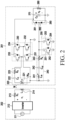
- FIG. 2 is a circuit diagram illustrating a wireless power transmission device and a wireless power reception device according to various embodiments.
- a wireless power transmission device 202 may include a power source 211, an inverter 212, and a transmission coil 214.
- the transmission coil 214 may have a parasitic resistor 213 with a resistance R 1 .
- the power source 211 may output direct current (DC) power, and the inverter 212 may convert the DC power received from the power source 211 into alternating current (AC) power.
- the transmission coil 214 may generate a magnetic field based on an AC voltage received from the inverter 212.
- a wireless power reception device 201 may include a first circuit 220, a first rectifier circuit 230, a second circuit 240, a detuning circuit 250, a second rectifier circuit 260, a capacitor 270, and a load 280.
- the first circuit 220 may include a first coil 221 and a first capacitor 222, and the first coil 221 may have a parasitic resistor 223 with a resistance R 2 .
- a first terminal of the first circuit 220 may be coupled to the ground, a first terminal of the second circuit 240, and a first input terminal of the first rectifier circuit 230.
- an induced electromotive force may be generated in the first coil 221.
- Generation of an induced electromotive force in the first coil 221 may be expressed as reception of wireless power in the first circuit 220 or the wireless power reception device 201.
- a second terminal of the first circuit 220 may be coupled to a second input terminal of the first rectifier circuit 230.
- the first rectifier circuit 230 may include four switches 231, 232, 233, and 234 which form a full bridge structure. Each of the four switches 231, 232, 233, and 234 may be an N-channel MOSFET and have a body diode.
- the first rectifier circuit 230 may rectify the wireless power received from the first circuit 220 from an AC form to a DC form, so that a rectified voltage V o is applied to both terminals of the capacitor 270.
- first terminals of the first switch 231 and the second switch 232 in the first rectifier circuit 230 may be coupled to the ground.
- a second terminal of the first switch 231, as the second input terminal of the first rectifier circuit 230, may be coupled to the second terminal of the first circuit 220, and a second terminal of the second switch 232, as the first input terminal of the first rectifier circuit 230, may be coupled to the first terminal of the first circuit 220.
- a point between the third switch 233 and the fourth switch 234 may be defined as an output terminal of the first rectifier circuit 230.
- a voltage applied to the gates of MOSFETs included in the four switches 231, 232, 233, and 234 may be controlled by a control circuit (not shown). An exemplary structure of the control circuit is described with reference to FIG. 5 .
- the control circuit may control turn-on of the four switches 231, 232, 233, and 234 by applying a voltage equal to or higher than the threshold voltage of the MOSFETs to the gates of the MOSFETs included in the four switches 231, 232, 233, and 234, and/or control turn-off of the four switches 231, 232, 233, and 234 by applying a voltage less than the threshold voltage of the MOSFETs to the gates of the MOSFETs.
- the second circuit 240 may include a second coil 241 and a second capacitor 242.
- the second coil 241 may have a parasitic resistor 243 with a resistance R a .
- the first terminal of the second circuit 240 may be coupled to the first terminal of the first circuit 220 and the ground, and a second terminal of the second circuit 240 may be coupled to the second rectifier circuit 260 and the detuning circuit 250.
- the detuning circuit 250 may include at least one detuning capacitor (e.g., detuning capacitors 251 and 253) and at least one detuning switch (e.g., detuning switches 252 and 254).
- detuning capacitors 251 and 253 and the two detuning switches 252 and 254 are illustrated in FIG. 2 , the number of detuning capacitors and the number of detuning switches included in the detuning circuit 250 are not limited according to various embodiments.
- the number of detuning capacitors included in the detuning circuit 250 may be equal to that of detuning switches included in the detuning circuit 250.
- a first terminal of the detuning circuit 250 may be coupled to the second terminal of the second circuit 240 and the second rectifier circuit 260, and a second terminal of the detuning circuit 250 may be coupled to the ground.
- each of the at least one detuning switch 252 and 254 may be an N-channel MOSFET and have a body diode. According to various embodiments, a voltage applied to the gates of MOSFETs included in the at least one detuning switch 252 and 254 may be controlled by the control circuit.
- the control circuit may control turn-on of the at least one detuning switch 252 and 254 by applying a voltage equal to or higher than the threshold voltage of the MOSFETs to the gates of the MOSFETs included in the at least one detuning switch 252 and 254 or turn-off of the at least one detuning switch 252 and 254 by applying a voltage less than the threshold voltage of the MOSFETs to the gates of the MOSFETs.
- the second rectifier circuit 260 may include two diodes (e.g., 261 and 262) forming a half bridge structure. Alternatively or additionally, the second rectifier circuit 260 may include two MOSFETs forming the half bridge structure. According to various embodiments, an output terminal of the second rectifier circuit 260 may be coupled to the output terminal of the first rectifier circuit 230.
- the load 280 may include a control circuit for generating a drive signal to control the four switches 231, 232, 233, and 234, and at least one detuning switch 252 and 254, a DC/DC converter, an LDO, and a battery.
- FIG. 3 is a flowchart illustrating exemplary operations performed by a wireless power reception device according to various embodiments.
- a control circuit of a wireless power reception device may identify a voltage at an output terminal of a rectifier circuit. For example, referring to FIG. 2 , the control circuit may identify the voltage V o of the output terminals of the first rectifier circuit 230 and the second rectifier circuit 260.
- the control circuit of the wireless power reception device 201 may control a detuning switch to an on state in response to the voltage V o of the output terminal of the rectifier circuit exceeding a first voltage.
- the control circuit may control the detuning switches 252 and 254 to the on state in response to the voltage V o of the output terminal exceeding the first voltage.
- the control circuit of the wireless power reception device 201 may control a first switch and a second switch of the rectifier circuit to the on state.
- the control circuit may control the first switch 231 and the second switch 232 of the first rectifier circuit 230 to the on state.
- the control circuit of the wireless power reception device 201 may control the third switch 233 and the fourth switch 234 of the first rectifier circuit 230 to an off state.
- the first coil 221, a closed-loop including the first switch 231, and the second switch 232 may be formed.
- the first coil 221, the first switch 231, the second switch 232, the first capacitor 222, and the parasitic resistor 223 may form a closed loop.
- FIG. 4A illustrates an equivalent circuit of a wireless power reception device according to various embodiments.
- FIG. 4A illustrates an equivalent circuit of the wireless power reception device 201 of FIG. 2 , when the first switch 231 and the second switch 232 of the first rectifier circuit 230 are controlled to the on state, and the third switch 233 and the fourth switch 234 of the first rectifier circuit 230 are controlled to the off state.
- the components illustrated in FIG. 4A correspond to the components illustrated in FIG. 2 , and similar reference numerals are used for the corresponding components.
- components through which no current flows are indicated by dotted lines (e.g., switches 433 and 434).
- an electromotive force induced in a first coil 421 based on a magnetic field generated by the wireless power transmission device 202 is represented as electromotive force V ind 424.
- V ind 424 an electromotive force induced in a first coil 421 based on a magnetic field generated by the wireless power transmission device 202
- V ind 424 an electromotive force induced in a first coil 421 based on a magnetic field generated by the wireless power transmission device 202
- V ind 424 an electromotive force induced in a first coil 421 based on a magnetic field generated by the wireless power transmission device 202.
- a current may flow in the closed loop including the first coil 421, the first switch 431, and the second switch 432 based on the electromotive force V ind 424 induced in the first coil 421.
- the first coil 421 may form a magnetic field, and an electromotive force may be induced in a second coil 441 based on the formed magnetic field.
- Power may be transferred to a load 480 based on the electromotive force induced in the second coil 441. That is, as the electromotive force is inducted in the second coil 441 based on the magnetic field formed by the current flowing in the closed loop including the first coil 421, the first switch 431 and the second switch 432 of the wireless power reception device 201 may receive wireless power.
- V L j V ind Z 0 R L ⁇ M 2 a z 0 + j ⁇ L 2 a + R a + 1 j ⁇ C s 2 + R L
- Equation 3 M 2a is the mutual inductance between the first coil 421 and the second coil 441.
- Z 0 may be expressed as Eq. 4.
- Z 0 ⁇ M 2 a 2 j ⁇ L 2 + R 2 + 1 j ⁇ C 2
- FIG. 4B illustrates an equivalent circuit of a wireless power reception device according to various embodiments.
- FIG. 4B illustrates an equivalent circuit of the wireless power reception device 201 of FIG. 2 , when the operations of FIG. 3 are performed.
- the components illustrated in FIG. 4B correspond to the components illustrated in FIG. 2 , and similar reference numerals are used for the corresponding components.
- components through which no current flows are indicated by dotted lines (e.g., switches 433 and 434, diodes 461 and 462, capacitor 470, and load 480).
- the first switch 231 and the second switch 232 of the first rectifier circuit 230 may be controlled to the on state
- the third switch 233 and the fourth switch 234 of the first rectifier circuit 230 may be controlled to the off state
- the at least one detuning switch 252 and 254 included in the detuning circuit 250 may be controlled to the on state.
- FIG. 4B is different from FIG. 4A in that the at least one detuning capacitor 451 and 453 may not be ignored.
- the voltage V L applied to the second rectifier circuit 260 is calculated by Eq. 5.
- V L j V ind Z 0 Z cmd ⁇ M 2 a z 0 + j ⁇ L 2 a + R a + 1 j ⁇ C s 2 + z cmd
- M 2a is the mutual inductance between the first coil 421 and the second coil 441.
- Z 0 may be expressed as Eq. 4.
- V L applied to the second rectifier circuit 260 may be approximated by Eq. 6.
- a current I coil flowing through the first coil 421 may be approximated by Eq. 7.
- a current I Qmd flowing through each of the at least one detuning switch 452 and 454 may be approximated by Eq. 8.
- Z 0 may be expressed as Eq. 4.
- Eqs. 7 and 8 A comparison between Eqs. 7 and 8 and Eq. 1 reveals that the current I coil flowing in the first coil 421 and the current I Qmd flowing through each of the at least one of the detuning switches 452 and 454 are smaller than those of Eq. 1 under the action of the mutual inductance between the first coil 421 and the second coil 441 in the circuit of FIG. 4B . Accordingly, the circuit of FIG. 4B may prevent an overcurrent from flowing through the first coil 421 and each of the at least one detuning switch 452 and 454.
- a closed loop including the first coil 421, the first switch 431, and the second switch 432 may be formed.
- the first coil 421, the first switch 431, the second switch 432, the first capacitor 422, and the parasitic resistor 423 may form the closed loop.
- a current may flow in the closed loop including the first coil 421, the first switch 431, and the second switch 432 based on the electromotive force V ind 424 induced in the first coil 421.
- the first coil 421 may form a magnetic field, and an electromotive force may be induced in the second coil 441 based on the formed magnetic field.
- the electromotive force is inducted in the second coil 441 based on the magnetic field formed by the current flowing in the closed loop including the first coil 421, the first switch 431 and the second switch 432 of the wireless power reception device 201 may receive wireless power.
- FIG. 5 illustrates a control circuit of a wireless power reception device (e.g., wireless power reception device 201 of FIG. 2 ) according to various embodiments.
- a control circuit 500 may include a first hysteresis comparator 510, a second hysteresis comparator 520, a multiplexer 530, a microprocessor 540, a first gate driver 550, and a second gate driver 560.
- the first hysteresis comparator 510 may compare a voltage V o at a particular point of the wireless power reception device 201 with a first voltage V high-OVP and a second voltage V low-OVP .
- the first voltage V high-OVP may be higher than the second voltage V low-OVP .
- the particular point of the wireless power reception device 201 may be the output terminal of the first rectifier circuit 230 and the second rectifier circuit 260 of FIG. 2 .
- the first hysteresis comparator 510 may transmit a high output signal V ovp to the multiplexer 530.
- the first hysteresis comparator 510 may transmit a low output signal V ovp to the multiplexer 530.
- the high output signal V ovp may indicate that an overvoltage is being induced in the wireless power reception device 201.
- the second hysteresis comparator 520 may compare the voltage V o at the particular point of the wireless power reception device 201 with a third voltage V high-UV and a fourth voltage V low-UV .
- the third voltage V high-UV may be higher than the fourth voltage V low-UV .
- the particular point of the wireless power reception device 201 may be the output terminal of the first rectifier circuit 230 and the second rectifier circuit 260 of FIG. 2 .
- the second hysteresis comparator 520 may transmit a low output signal Vuv to the multiplexer 530.
- the second hysteresis comparator 520 may transmit a high output signal Vuv to the multiplexer 530.
- the low output signal Vuv may indicate that too low a voltage is being induced in the wireless power reception device 201.
- the microprocessor 540 may transmit an output signal V s2p indicating whether the resonance circuit of the wireless power reception device 201 is to receive wireless power by series resonance or parallel resonance to the multiplexer 530.
- a high output signal V s2p indicates that the resonant circuit of the wireless power reception device 201 is preferably to receive wireless power by parallel resonance
- a low output signal V s2p indicates that the resonance circuit of the wireless power reception device 201 is preferably to receive wireless power by series resonance.
- the first circuit 220 and the second circuit 240 of the wireless power reception device 201 illustrated in FIG. 2 may form a resonance circuit.
- the resonance circuit of the wireless power reception device 201 may receive wireless power by series resonance.
- the resonance circuit of the wireless power reception device 201 receives wireless power by series resonance, this may imply that wireless power is received by an induced electromotive force generated in the first coil 221 and the second coil 241 based on a magnetic field generated by the wireless power transmission device 202.
- the resonance circuit of the wireless power reception device 201 may receive wireless power by parallel resonance.
- the resonance circuit of the wireless power reception device 201 receives wireless power by parallel resonance, this may imply that as an induced electromotive force is generated in the first coil 221 based on a magnetic field generated by the wireless power transmission device 202, and an induced electromotive force is generated in the second coil 241 based on a magnetic field generated by the first coil 221, wireless power is received.
- the first gate driver 550 may output a driving signal for controlling on/off of the at least one detuning switch 252 and 254 included in the detuning circuit (e.g., the detuning circuit 250) based on a control signal from the multiplexer 530.
- the second gate driver 560 may output a driving signal for controlling on/off of the four switches 231, 232, 233 and 234 included in the rectifier circuit (e.g., the first rectifier circuit 230) based on a control signal from the multiplexer 530.
- the multiplexer 530 may control the first gate driver 550 and the second gate driver 560 based on the signal V ovp received from the first hysteresis comparator 510 and the signal V s2p received from the microprocessor 540.
- the multiplexer 530 may control the first gate driver 550 to output a driving signal for controlling the at least one detuning switch 252 and 254 to the on state, and control the second gate driver 560 to output a driving signal for controlling the first switch 231 and the second switch 232 to the on state and the third switch 233 and the fourth switch 234 to the off state among the four switches 231, 232, 233, and 234.
- the multiplexer 530 may control the second gate driver 560 a predetermined time after control of the first gate driver 550.
- the multiplexer 530 may control the first gate driver 550 to output a driving signal for controlling the at least one detuning switch 252 and 254 to the onstate, and control the second gate driver 560 to output a driving signal for controlling the first switch 231 and the second switch 232 to the on state and the third switch 233 and the fourth switch 234 to the off state among the four switches 231, 232, 233, and 234.
- the multiplexer 530 may control the second gate driver 560 a predetermined time after control of the first gate driver 550.
- the multiplexer 530 may control the first gate driver 550 to output a driving signal for controlling the at least one detuning switch 252 and 254 to the off state, and control the second gate driver 560 to output a driving signal for controlling the first switch 231 and the second switch 232 to the on state and the third switch 233 and the fourth switch 234 to the off state among the four switches 231, 232, 233, and 234.
- the multiplexer 530 may control the second gate driver 560 a predetermined time after control of the first gate driver 550.
- the multiplexer 530 may control the first gate driver 550 to output a driving signal for controlling the at least one detuning switch 252 and 254 to the off state, and control the second gate driver 560 to output a driving signal for controlling the four switches 231, 232, 233, and 234 to the off state or controlling the four switches 231, 232, 233, and 234 synchronously.
- the multiplexer 530 may control the first gate driver 550 a predetermined time after control of the second gate driver 560.
- the multiplexer 530 may control the first gate driver 550 and the second gate driver 560, further relying on the signal Vuv received from the second hysteresis comparator 520 in addition to the signal V ovp received from the first hysteresis comparator 510 and the signal V s2p received from the microprocessor 540.
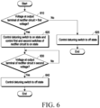
- FIG. 6 illustrates exemplary operations performed by a wireless power reception device according to various embodiments.
- a control circuit e.g., the control circuit 500 of a wireless power reception device (e.g., the wireless power reception device 201) may identify whether a voltage of an output terminal of a rectifier circuit is higher than a first voltage.
- the control circuit 500 may identify whether the voltage V o at the output terminals of the first rectifier circuit 230 and the second rectifier circuit 260 is higher than the first voltage.
- an overvoltage may be applied to the wireless power reception device 201.
- the control circuit 500 of the wireless power reception device 201 may control a detuning switch (e.g., the at least one detuning switch 252 and 254) to the off state in operation 625.
- a detuning switch e.g., the at least one detuning switch 252 and 254
- the control circuit 500 of the wireless power reception device 201 may control switches of the rectifier circuit (e.g., the four switches 231, 232, 233, and 234 of the first rectifier circuit 230) to the off state or synchronously control the switches of the rectifier circuit.
- the control circuit 500 of the wireless power reception device 201 may synchronously control the switches of the rectifier circuit, whereas when the magnitude of received wireless power is smaller than the specific magnitude, the control circuit 500 may control the switches of the rectifier circuit to the off state.
- the control circuit 500 of the wireless power reception device 201 may control the at least one detuning switch 252 and 254 to the off state.
- control circuit 500 of the wireless power reception device 201 may control the first switch 231 and the second switch 232 to the on state and the third switch 233 and the fourth switch 234 to the off state among the switches of the rectifier circuit (e.g., the four switches 231, 232, 233, and 234 of the first rectifier circuit 230).
- the control circuit 500 of the wireless power reception device 201 may control the first switch 231 and the second switch 232 to the on state and the third switch 233 and the fourth switch 234 to the off state among the switches of the rectifier circuit (e.g., the four switches 231, 232, 233, and 234 of the first rectifier circuit 230), after controlling the at least one detuning switch 252 and 254 to the off state.
- the switches of the rectifier circuit e.g., the four switches 231, 232, 233, and 234 of the first rectifier circuit 230
- the control circuit 500 of the wireless power reception device 201 may control a detuning switch (e.g., the at least one detuning switch 252 and 254) to the on state, and control the first switch (e.g., the first switch 231) and the second switch (e.g., the second switch 232) of the rectifier circuit (e.g., the first rectifier circuit 230) to the on state in operation 620.
- a detuning switch e.g., the at least one detuning switch 252 and 254
- the first switch e.g., the first switch 231
- the second switch e.g., the second switch 232
- control circuit 500 of the wireless power reception device 201 may control the first switch 231 and the second switch 232 of the first rectifier circuit 230 to the on state, after controlling the detuning switch (e.g., the at least one detuning switch 252 and 254) to the on state.
- control circuit 500 of the wireless power reception device 201 may control the third switch 233 and the fourth switch 234 to the off state among the four switches 231, 232, 233, and 234 of the first rectifier circuit 230.
- control circuit 500 of the wireless power reception device 201 may identify whether the voltage at the output terminal of the rectifier circuit (e.g., the voltage V o at the output terminal of the first rectifier circuit 230) is less than or equal to a second voltage.
- the second voltage may be lower than the first voltage.
- control circuit 500 of the wireless power reception device 201 may repeat operation 630 until the voltage of the output terminal of the rectifier circuit is identified as less than or equal to the second voltage.
- control circuit 500 of the wireless power reception device 201 may control the detuning switch (e.g., the at least one detuning switch 252 and 254) to the off state in operation 640.
- the detuning switch e.g., the at least one detuning switch 252 and 254
- details of operation 625 may be equally applied to operation 640.
- FIG. 7 is a circuit diagram illustrating a wireless power transmission device and a wireless power reception device according to various embodiments.
- a wireless power transmission device 702 may include a power source 711, an inverter 712, and a transmission coil 714. Details of the power source 211, the inverter 212, and the transmission coil 214 described above with reference to FIG. 2 may be equally applied to the power source 711, the inverter 712, and the transmission coil 714 of FIG. 7 , respectively.
- a wireless power reception device 701 may include a first circuit 720, a first rectifier circuit 730, a second circuit 740, a third circuit 745, a first detuning circuit 750, a second detuning circuit 755, a second rectifier circuit 760, a capacitor 770, and a load 780.
- Details of the first circuit 220, the first rectifier circuit 230, the second circuit 240, the capacitor 270, and the load 280 described above with reference to FIG. 2 may be equally applied to the first circuit 720, the first rectifier circuit 730, the second circuit 740, the capacitor 770, and the load 780 of FIG. 7 , respectively.
- the third circuit 745 may include a third coil 746 and a third capacitor 747, and the third coil 746 may include a parasitic resistor 748 with a resistance R b . Like a second coil 741, the third coil 746 may be magnetically coupled to a first coil 721.
- the third circuit 745 may have a first terminal coupled to the first circuit 720, the second circuit 740, and the ground, and a second terminal coupled to the second detuning circuit 755 and a second input terminal of the second rectifier circuit 760.
- the second detuning circuit 755 may include a second detuning capacitor 756 and a second detuning switch 757. While the second detuning circuit 755 is shown in FIG. 7 as including one second detuning capacitor 756 and one second detuning switch 757, the second detuning circuit 755 may include a plurality of second detuning capacitors 756 and a plurality of second detuning switches 757 according to various embodiments.
- the second circuit 740 may have a first terminal coupled to the first circuit 720, the third circuit 745, and the ground, and a second terminal coupled to the first detuning circuit 750 and a first input terminal of the second rectifier circuit 760.
- the first detuning circuit 750 may include a first detuning capacitor 751 and a first detuning switch 752. While the first detuning circuit 750 is shown in FIG. 7 as including one first detuning capacitor 751 and one first detuning switch 752, the first detuning circuit 750 may include a plurality of first detuning capacitors 751 and a plurality of first detuning switches 752 according to various embodiments.
- the second rectifier circuit 760 may include four switches 761, 762, 763, and 764 which form a full bridge structure.
- a voltage applied to the gates of MOSFETs included in the four switches 761, 762, 763, and 764 may be controlled by a control circuit (e.g., the control circuit 500).
- the control circuit 500 may control the four switches 761, 762, 763, and 764 to the on state by applying a voltage equal to or higher than the threshold voltage of the MOSFETs to the gates of the MOSFETs included in the four switches 761, 762, 763, and 764, or control the four switches 761, 762, 763, and 764 to the off state by applying a voltage lower than the threshold voltage of the MOSFETs to the gates of the MOSFETs. While the four switches 761, 762, 763, and 764 are shown as including MOSFETs in FIG. 7 , the second rectifier circuit 760 may be implemented with four diodes forming a full bridge structure according to various embodiments. According to various embodiments, an output terminal of the second rectifier circuit 760 may be coupled to an output terminal of the first rectifier circuit 730.
- FIGS. 3 and 6 have been described mainly with respect to the wireless power reception device 201 of FIG. 2 , the operations of FIGS. 3 and 6 may also be performed in the wireless power reception device 701 of FIG. 7 according to various embodiments.
- the control circuit 500 may identify a voltage V o at the output terminals of the first rectifier circuit 730 and the second rectifier circuit 760.
- the control circuit 500 may control the first detuning switch 752 and the second detuning switch 757 to the on state.
- the control circuit 500 may control the first switch 731 and the second switch 732 of the first rectifier circuit 730 to the on state. In this case, the control circuit 500 may control the third switch 733 and the fourth switch 734 of the first rectifier circuit 730 to the off state.
- the control circuit 500 may control the four switches 761, 762, 763, and 764 of the second rectifier circuit 760 to the off state or may control the four switches synchronously.
- the control circuit 500 may synchronously control the four switches 761, 762, 763, and 764 in operation 330.
- the control circuit 500 may control the four switches 761, 762, 763, and 764 to the off state in operation 330.
- the control circuit 500 may control the first detuning switch 752 and the second detuning switch 757 to the on state, and control the first switch 731 and the second switch 732 of the first rectifier circuit 730 to the on state.
- the control circuit 500 may control the four switches 761, 762, 763, and 764 of the second rectifier circuit 760 to the off state or synchronously.
- control circuit 500 may control the first detuning switch 752 and the second detuning switch 757 to the off state.
- FIG. 6 may also be applied in the same manner, when the operations of FIG. 6 are performed in the wireless power reception device 701 of FIG. 7 .
- FIG. 8 is a circuit diagram illustrating a wireless power transmission device and a wireless power reception device according to various embodiments.
- a wireless power transmission device 802 may include a power source 811, an inverter 812, and a transmission coil 814.
- the details of the power source 211, the inverter 212, and the transmission coil 214 described before with reference to FIG. 2 may be equally applied to the power source 811, the inverter 812, and the transmission coil 814 of FIG. 8 , respectively.
- the details of the power source 711, the inverter 712, and the transmission coil 714 described before with reference to FIG. 7 may be equally applied to the power source 811, the inverter 812, and the transmission coil 814 of FIG. 8 , respectively.
- a wireless power reception device 801 may include a first circuit 820, a rectifier circuit 830, a second circuit 840, a detuning circuit 850, a capacitor 870, and a load 880.
- the details of the first circuit 220, the first rectifier circuit 230, the second circuit 240, the detuning circuit 250, the capacitor 270, and the load 280 described above with reference to FIG. 2 may be equally applied to the first circuit 820, the rectifier circuit 830, the second circuit 840, the detuning circuit 850, the capacitor 870, and the load 880 of FIG. 8 , respectively.
- the details of the first circuit 720, the first rectifier circuit 730, the second circuit 740, the first detuning circuit 750, the capacitor 770, and the load 780 described above with reference to FIG. 7 may be equally applied to the first circuit 820, the rectifier circuit 830, the second circuit 840, the detuning circuit 850, the capacitor 870, and the load 880 of FIG. 8 , respectively.
- FIGS. 3 and 6 have been described mainly with respect to the wireless power reception device 201 of FIG. 2 and the wireless power reception device 701 of FIG. 7 , the operations of FIGS. 3 and 6 may also be performed in the wireless power reception device 801 of FIG. 8 according to various embodiments.
- a control circuit 500 may identify a voltage V o at an output terminal of the rectifier circuit 830.
- the control circuit 500 may control detuning switches 851 and 853 to the on state.
- the control circuit 500 may control a first switch 731 and a second switch 832 of the rectifier circuit 830 to the on state.
- the control circuit 500 may control a third switch 833 and a fourth switch 834 of the rectifier circuit 830 to the off state.
- the control circuit 500 may control the detuning switches 851 and 853 to the on state, and control the first switch 831 and the second switch 832 of the rectifier circuit 830 to the on state.
- the control circuit 500 may control the detuning switches 851 and 853 to the off state.
- the details of FIG. 6 described before with reference to FIG. 2 and to FIG. 7 may also be applied in the same manner, when the operations of FIG. 6 are performed in the wireless power reception device 801 of FIG. 8 .
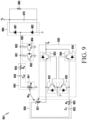
- FIG. 9 is a circuit diagram illustrating a wireless power reception device according to various embodiments.
- a wireless power reception device 901 may include a first circuit 920, a first rectifier circuit 930, a second circuit 940, a detuning circuit 950, a second rectifier circuit 960, a capacitor 970, and a load 980.
- the first circuit 920 may include a first coil 921 and a first capacitor 922, and the first coil 921 may have a parasitic resistor 923 with a resistance R 2 .
- the first circuit 920 may have a first terminal coupled to a first input terminal of the first rectifier circuit 930 and a second terminal coupled to a second input terminal of the first rectifier circuit 930.
- an induced electromotive force may be generated in the first coil 921.
- Generation of an induced electromotive force in the first coil 921 may be expressed as reception of wireless power in the first circuit 920 or the wireless power reception device 901.
- the first rectifier circuit 930 may include four switches 931, 932, 933, and 934 which form a full bridge structure.
- Each of the four switches 931, 932, 933, and 934 may be an N-channel MOSFET and have a body diode.
- the first rectifier circuit 930 may rectify the wireless power received from the first circuit 920 from an AC form to a DC form, so that a rectified voltage V o is applied to both terminals of the capacitor 970.
- first terminals of a first switch 931 and a second switch 932 in the first rectifier circuit 930 may be coupled to the ground.
- a point between the third switch 933 and the fourth switch 934 may be defined as an output terminal of the first rectifier circuit 930.
- a voltage applied to the gates of MOSFETs included in the four switches 931, 932, 933, and 934 may be controlled by a control circuit (e.g., the control circuit 500).
- the control circuit 500 may control the four switches 931, 932, 933, and 934 to the on state by applying a voltage equal to or higher than the threshold voltage of the MOSFETs to the gates of the MOSFETs included in the four switches 931, 932, 933, and 934, or control the four switches 931, 932, 933, and 934 to the off state by applying a voltage lower than the threshold voltage of the MOSFETs to the gates of the MOSFETs.
- the second circuit 940 may include a second coil 941 and a second capacitor 942.
- the second coil 941 may have a parasitic resistor 943 with a resistance R a .
- a first terminal of the second circuit 940 may be coupled to the ground, and a second terminal of the second circuit 940 may be coupled to the second rectifier circuit 960 and the detuning circuit 950.
- the detuning circuit 950 may include at least one detuning capacitor 951 and 953 and at least one detuning switch 952 and 954. Although the two detuning capacitors 951 and 953 and the two detuning switches 952 and 954 are illustrated in FIG. 9 , the number of detuning capacitors and the number of detuning switches included in the detuning circuit 950 are not limited according to various embodiments. According to various embodiments, the number of detuning capacitors included in the detuning circuit 950 may be equal to that of detuning switches included in the detuning circuit 950. According to various embodiments, a first terminal of the detuning circuit 950 may be coupled to a second terminal of the second circuit 940 and the second rectifier circuit 960, and a second terminal of the detuning circuit 950 may be coupled to the ground.
- each of the at least one detuning switch 952 and 954 may be an N-channel MOSFET and have a body diode. According to various embodiments, a voltage applied to the gates of MOSFETs included in the at least one detuning switch 952 and 954 may be controlled by the control circuit 500.
- the control circuit 500 may control the at least one detuning switch 952 and 954 to the on state by applying a voltage equal to or greater than the threshold voltage of the MOSFETs to the gates of the MOSFETs included in the at least one detuning switch 952 and 954 or control the at least one detuning switch 952 and 954 to the off state by applying a voltage less than the threshold voltage of the MOSFETs to the gates of the MOSFETs.
- the second rectifier circuit 960 may include two diodes 961 and 962 forming a half bridge structure. Alternatively or additionally, the second rectifier circuit 960 may include two MOSFETs forming the half bridge structure. According to various embodiments, an output terminal of the second rectifier circuit 960 may be coupled to the output terminal of the first rectifier circuit 930.
- the load 980 may include a control circuit 500 for generating a drive signal to control the four switches 931, 932, 933, and 934, and the at least one detuning switch 952 and 954, a DC/DC converter, an LDO, and a battery.
- FIGS. 3 and 6 have been described mainly with respect to the wireless power reception device 201 of FIG. 2 , the wireless power reception device 701 of FIG. 7 , and the wireless power reception device 801 of FIG. 8 , the operations of FIGS. 3 and 6 may also be performed in the wireless power reception device 901 of FIG. 9 .
- the wireless power reception device 201 for receiving wireless power from the wireless power transmission device 202 may include the first circuit 220, the first rectifier circuit 230, the second circuit 240, the detuning circuit 250, and the control circuit.
- the first circuit 220 may include the first coil 221, and the first terminal of the first circuit 220 may be coupled to the ground and the first terminal of the first rectifier circuit 230.
- the first rectifier circuit 230 may include the plurality of switches 231, 232, 233, and 234, and the first terminal of the first switch 231 and the first terminal of the second switch 232 among the plurality of switches 231, 232, 233, and 234 may be coupled to the ground.
- the second circuit 240 may include the second coil 241.
- the first terminal of the second circuit 240 may be coupled to the ground and the first terminal of the first circuit 220.
- the second terminal of the second circuit 240 may be coupled to the first terminal of the detuning circuit 250.
- the detuning circuit 250 may include the at least one detuning capacitor 251 and 253 and the at least one detuning switch 252 and 254, and the second terminal of the detuning circuit 250 may be coupled to the ground.
- control circuit In response to a voltage at the output terminal of the first rectifier circuit 230 exceeding a first voltage, the control circuit is configured to form a closed loop including the first coil 221, the first switch 231, and the second switch 232 by controlling the at least one detuning switch 252 and 254 to the on state and controlling the first switch 231 and the second switch 232 to the on state.
- the wireless power reception device may be configured to receive the wireless power by an electromotive force induced in the second coil 241 based on a magnetic field formed by a current flowing in the closed loop including the first coil 221, the first switch 231, and the second switch 232.
- control circuit in response to the voltage at the output terminal of the first rectifier circuit 230 exceeding the first voltage, the control circuit may be configured to control the first switch 231 and the second switch 232 to the on state, after controlling the at least one detuning switch 252 and 254 to the on state.
- control circuit may be configured to identify that the voltage at the output terminal of the first rectifier circuit 230 is lower than or equal to a second voltage, while the at least one detuning switch 252 and 254 is controlled to the on state, and the first switch 231 and the second switch 232 are controlled to the on state, and in response to the voltage at the output terminal of the first rectifier circuit 230 being identified as lower than or equal to the second voltage, control the at least one detuning switch 252 and 254 to an off state.
- control circuit in response to the voltage at the output terminal of the first rectifier circuit 230 being identified as lower than or equal to the second voltage, the control circuit is configured to control the plurality of switches 231, 232, 233, and 234 to the off state.
- control circuit in response to the voltage at the output terminal of the first rectifier circuit 230 being identified as lower than or equal to the second voltage, the control circuit may be configured to control the at least one detuning switch 252 and 254 to the off state after controlling the plurality of switches 231, 232, 233, and 234 to the off state.
- control circuit in response to the voltage at the output terminal of the first rectifier circuit 230 being identified as lower than or equal to the second voltage, the control circuit may be configured to control the plurality of switches 231, 232, 233, and 234 synchronously.
- control circuit in response to the voltage at the output terminal of the first rectifier circuit 230 being identified as lower than or equal to the second voltage, the control circuit may be configured to control the at least one detuning switch 252 and 254 to the off state after controlling the plurality of switches 231, 232, 233, and 234 synchronously.
- the wireless power reception device 901 may further include the second rectifier circuit 260 coupled to the second terminal of the second circuit 240 and the first terminal of the at least one detuning circuit 250, and then output terminal of the second rectifier circuit 260 may be coupled to the output terminal of the first rectifier circuit 230.
- the second rectifier circuit 260 may be a half bridge rectifier circuit.
- the wireless power reception device may further include the third circuit 745 including the third coil 746, and the second detuning circuit 755.
- the first terminal of the third circuit 745 may be coupled to the ground, the first terminal of the first circuit 720, and the first terminal of the second circuit 740.
- the second detuning circuit 755 may include the at least one second detuning capacitor 756 and the at least one second detuning switch 757.
- the second terminal of the third circuit 745 may be coupled to the first terminal of the second detuning circuit 755.
- the second terminal of the second detuning circuit 755 may be coupled to the ground.
- the second rectifier circuit 760 may be coupled to the second terminal of the third circuit 745.
- the second rectifier circuit 760 may be a full bridge rectifier circuit.
- the wireless power reception device 901 for receiving wireless power from a wireless power transmission device may include the first circuit 920, the first rectifier circuit 930, the second circuit 940, the detuning circuit 950, the second rectifier circuit 960, and the control circuit.
- the first circuit 920 may include the first coil 921, and the first terminal and the second terminal of the first circuit 920 are coupled to the first rectifier circuit 930.
- the first rectifier circuit 930 may include the plurality of switches 931, 932, 933, and 934, and the first terminal of the first switch 931 and the first terminal of the second switch 932 among the plurality of switches 931, 932, 933, and 934 may be coupled to the ground.
- the second circuit 940 may include the second coil 941.
- the first terminal of the second circuit 940 may be coupled to the ground.
- the second terminal of the second circuit 940 may be coupled to the first terminal of the detuning circuit 950.
- the detuning circuit 950 may include the at least one detuning capacitor 951 and 953 and the at least one detuning switch 952 and 954, and the second terminal of the detuning circuit 950 may be coupled to the ground.
- the second rectifier circuit 960 may be coupled to the second terminal of the first circuit 920 and the first terminal of the detuning circuit 950, and the output terminal of the second rectifier circuit 960 may be coupled to the output terminal of the first rectifier circuit 930.
- control circuit may be configured to control the at least one detuning switch 952 and 954 to an on state and control the first switch 931 and the second switch 932 to the on state.
- a method of controlling the wireless power reception device 201 including the first circuit 220 including the first coil 221 for receiving wireless power, the second circuit 240 including the second coil 241, the rectifier circuit configured to rectify the wireless power, and the detuning circuit 250 coupled to the second circuit 240 may include identifying a voltage at the output terminal of the rectifier circuit of the wireless power reception device 201, controlling the at least one detuning switch 252 and 254 included in the detuning circuit 250 of the wireless power reception device 201 to an on state, in response to the voltage at the output terminal of the rectifier circuit exceeding a first voltage, and forming a closed loop by the first coil 221, the first switch 231, and the second switch 232 by controlling the first switch 231 of the wireless power reception device 201 and the second switch 232 of the wireless power reception device 201 which are coupled to the ground to the on state among the plurality of switches 231, 232, 233, and 234 included in the rectifier circuit.
- the controlling of the first switch 231 and the second switch 232 may comprise controlling the first switch 231 and the second switch 232 to the on state after the controlling of the at least one detuning switch 252 and 254 to the on state.
- the method may further include controlling the third switch and the fourth switch among the plurality of switches 231, 232, 233, and 234 to an off state, in response to the voltage at the output terminal of the rectifier circuit exceeding the first voltage.
- the method may further include identifying that the voltage at the output terminal of the rectifier circuit is lower than or equal to a second voltage, while the at least one detuning switch 252 and 254 is controlled to the on state, and the first switch 231 and the second switch 234 are controlled to the on state, and in response to the voltage at the output terminal of the rectifier circuit being identified as lower than or equal to the second voltage, controlling the at least one detuning switch 252 and 254 to the off state.
- the method may further include controlling the plurality of switches 231, 232, 233, and 234 to the off state, in response to the voltage at the output terminal of the rectifier circuit being identified as lower than or equal to the second voltage.
- the controlling of the at least one detuning switch 252 and 254 to the off state may comprise controlling the at least one detuning switch 252 and 254 to the off state after the controlling of the plurality switches 231, 232, 233, and 234 to the off state.
- the method may further comprise controlling the plurality of switches 231, 232, 233, and 234 synchronously, in response to the voltage at the output terminal of the rectifier circuit being identified as lower than or equal to the second voltage.
- the controlling of the at least one detuning switch 252 and 254 to the off state may comprise controlling the at least one detuning switch 252 and 254 to the off state after the controlling of the plurality of switches 231, 232, 233, and 234 synchronously.
- the wireless power reception device 201 for receiving wireless power from the wireless power transmission device 202 may include the first circuit 220, the first rectifier circuit 230, the second circuit 240, the detuning circuit 250, and the control circuit.
- the first circuit 220 may include the first coil 221, and the first terminal of the first circuit 220 may be coupled to the ground and the first terminal of the first rectifier circuit 230.
- the first rectifier circuit 230 may include the plurality of switches 231, 232, 233, and 234, and the first terminal of the first switch 231 and the first terminal of the second switch 232 among the plurality of switches 231, 232, 233, and 234 may be coupled to the ground.
- the second circuit 240 may include the second coil 241.
- the first terminal of the second circuit 240 may be coupled to the ground and the first terminal of the first circuit 220.
- the second terminal of the second circuit 240 may be coupled to the first terminal of the detuning circuit 250.
- the detuning circuit 250 may include the at least one detuning capacitor 251 and 253 and the at least one detuning switch 252 and 254, and the second terminal of the detuning circuit 250 may be coupled to the ground.
- the control circuit may be configured to identify that the voltage at the output terminal of the first rectifier circuit 230 is lower than or equal to a first voltage, while the at least one detuning switch 252 and 254 is controlled to the on state, and the first switch 231 and the second switch 232 are controlled to the on state, and in response to the voltage at the output terminal of the first rectifier circuit 230 being identified as lower than or equal to the first voltage, control the at least one detuning switch 252 and 254 to an off state.
- the control circuit in response to the voltage at the output terminal of the first rectifier circuit 230 exceeding a second voltage, is configured to form a closed loop including the first coil 221, the first switch 231, and the second switch 232 by controlling the at least one detuning switch 252 and 254 to the on state and controlling the first switch 231 and the second switch 232 to the on state.
- control circuit in response to the voltage at the output terminal of the first rectifier circuit 230 being identified as lower than or equal to the first voltage, the control circuit is configured to control the four switches 231, 232, 233, and 234 to the off state.
- control circuit in response to the voltage at the output terminal of the first rectifier circuit 230 being identified as lower than or equal to the first voltage, the control circuit is configured to control the at least one detuning switch 252 and 254 to the off state after controlling the four switches 231, 232, 233, and 234 to the off state.
- the wireless power reception device may be one of various types of electronic devices.
- the wireless power reception device may include, for example, a portable communication device (e.g., a smartphone), a computer device, a portable multimedia device, a portable medical device, a camera, a wearable device, or a home appliance.
- a portable communication device e.g., a smartphone
- a computer device e.g., a laptop, a desktop, a tablet, or a portable multimedia device.
- a portable medical device e.g., a portable medical device
- camera e.g., a camera
- a wearable device e.g., a portable medical device
- each of such phrases as “A or B”, “at least one of A and B”, “at least one of A or B”, “A, B, or C”, “at least one of A, B, and C”, and “at least one of A, B, or C” may include any one of, or all possible combinations of the items enumerated together in a corresponding one of the phrases.
- such terms as “1st” and “2nd” or “first” and “second” may be used to simply distinguish a corresponding component from another, and does not limit the components in other aspect (e.g., importance or order).
- an element e.g., a first element
- the element may be coupled with the other element directly (e.g., wiredly), wirelessly, or via a third element.
- module may include a unit implemented in hardware, software, or firmware, and may interchangeably be used with other terms, for example, logic, logic block, part, or circuitry.
- a module may be a single integral component, or a minimum unit or part thereof, adapted to perform one or more functions.
- the module may be implemented in a form of an application-specific integrated circuit (ASIC).
- ASIC application-specific integrated circuit
- Various embodiments as set forth herein may be implemented as software (e.g., a program) including one or more instructions that are stored in a storage medium (e.g., an internal memory or an external memory) that is readable by a machine (e.g., an electronic device).
- a processor e.g., the processor 540
- the machine e.g., the electronic device, a wireless power reception device
- the one or more instructions may include a code generated by a complier or a code executable by an interpreter.
- the machine-readable storage medium may be provided in the form of a non-transitory storage medium.
- the term 'non-transitory' simply means that the storage medium is a tangible device, and does not include a signal (e.g., an electromagnetic wave), but this term does not differentiate between where data is semi-permanently stored in the storage medium and where the data is temporarily stored in the storage medium.
- a method may be included and provided in a computer program product.
- the computer program product may be traded as a product between a seller and a buyer.
- the computer program product may be distributed in the form of a machine-readable storage medium (e.g., compact disc read only memory (CD-ROM)), or be distributed (e.g., downloaded or uploaded) online via an application store (e.g., PlayStore TM ), or between two user devices (e.g., smart phones) directly. If distributed online, at least part of the computer program product may be temporarily generated or at least temporarily stored in the machine-readable storage medium, such as memory of the manufacturer's server, a server of the application store, or a relay server.
- CD-ROM compact disc read only memory
- an application store e.g., PlayStore TM
- two user devices e.g., smart phones
- each component e.g., a module or a program of the above-described components may include a single entity or multiple entities, and some of the multiple entities may be separately disposed in different components. According to various embodiments, one or more of the above-described components may be omitted, or one or more other components may be added. Alternatively or additionally, a plurality of components (e.g., modules or programs) may be integrated into a single component. In such a case, according to various embodiments, the integrated component may still perform one or more functions of each of the plurality of components in the same or similar manner as they are performed by a corresponding one of the plurality of components before the integration.
- operations performed by the module, the program, or another component may be carried out sequentially, in parallel, repeatedly, or heuristically, or one or more of the operations may be executed in a different order or omitted, or one or more other operations may be added.
Landscapes
- Engineering & Computer Science (AREA)
- Power Engineering (AREA)
- Computer Networks & Wireless Communication (AREA)
- Rectifiers (AREA)
Abstract
Description
- The present disclosure relates to a wireless power reception device including a detuning circuit.
- Electronic devices such as smartphones have recently adopted electromagnetic induction-based wireless charging or magnetic resonance-based wireless charging. When a power transmitting unit (PTU) (e.g., a wireless charging pad) and a power receiving unit (PRU) (e.g., a smartphone) come into contact with each other or approach within a certain distance, the battery of the PRU may be charged by electromagnetic induction or electromagnetic resonance between the transmission coil of the PTU and the reception coil of the PRU.
- When the PTU induces too high a voltage to the PRU, the PRU may be damaged. The PRU may include a detuning circuit configured to couple one or more additional capacitors to a resonance circuit, when the voltage of received wireless power exceeds a specific level.
- According to various embodiments, a wireless power reception device for receiving wireless power from a wireless power transmission device may include a first circuit, a first rectifier circuit, a second circuit, a detuning circuit, and a control circuit. The first circuit may include a first coil, and a first terminal of the first circuit may be coupled to a ground and to a first terminal of the first rectifier circuit. The first rectifier circuit may include a plurality of switches, a first terminal of a first switch and a first terminal of a second switch among the plurality of switches may be coupled to the ground. The second circuit may include a second coil. A first terminal of the second circuit may be coupled to the ground and the first terminal of the first circuit. A second terminal of the second circuit may be coupled to a first terminal of the detuning circuit. The detuning circuit may include at least one detuning capacitor and at least one detuning switch, and a second terminal of the detuning circuit may be coupled to the ground. In response to a voltage at an output terminal of the first rectifier circuit exceeding a first voltage, the control circuit may be configured to form a closed loop including the first coil, the first switch, and the second switch by controlling the at least one detuning switch to an on state and controlling the first switch and the second switch to the on state.
- According to various embodiments, a method of controlling a wireless power reception device may include identifying a voltage at an output terminal of a rectifier circuit of the wireless power reception device, controlling at least one detuning switch included in a detuning circuit of the wireless power reception device to an on state, in response to the voltage at the output terminal of the rectifier circuit exceeding a first voltage, and forming a closed loop by a first coil of the wireless power reception device, a first switch of the wireless power reception device, and a second switch of the wireless power reception device by controlling the first switch and the second switch which are coupled to a ground to the on state among a plurality of switches included in the rectifier circuit.
- According to various embodiments, a wireless power reception device for receiving wireless power from a wireless power transmission device may include a first circuit, a first rectifier circuit, a second circuit, a detuning circuit, a second rectifier circuit, and a control circuit. The first circuit may include a first coil, and a first terminal and a second terminal of the first circuit may be coupled to the first rectifier circuit. The first rectifier circuit may include a plurality of switches, a first terminal of a first switch and a first terminal of a second switch among the plurality of switches may be coupled to a ground. The second circuit may include a second coil. A first terminal of the second circuit may be coupled to the ground. A second terminal of the second circuit may be coupled to a first terminal of the detuning circuit. The detuning circuit may include at least one detuning capacitor and at least one detuning switch, and a second terminal of the detuning circuit may be coupled to the ground. The second rectifier circuit may be coupled to the second terminal of the first circuit and the first terminal of the detuning circuit, and an output terminal of the second rectifier may be coupled to an output terminal of the first rectifier circuit. In response to a voltage at the output terminal of the first rectifier circuit exceeding a first voltage, the control circuit may be configured to control the at least one detuning switch to an on state and control the first switch and the second switch to the on state.
- According to various embodiments, a wireless power reception device for receiving wireless power from a wireless power transmission device may comprise a first circuit, a first rectifier circuit, a second circuit, a detuning circuit, and a control circuit. The first circuit may include a first coil, and a first terminal of the first circuit is coupled to a ground and to a first terminal of the first rectifier circuit. The first rectifier circuit may include four switches, and a first terminal of a first switch and a first terminal of a second switch among the four switches are coupled to the ground. The second circuit may include a second coil, a first terminal of the second circuit is coupled to the ground and the first terminal of the first circuit, and a second terminal of the second circuit is coupled to a first terminal of the detuning circuit. The detuning circuit may include at least one detuning capacitor and at least one detuning switch, and a second terminal of the detuning circuit is coupled to the ground. The control circuit may be configured to identify that a voltage at an output terminal of the first rectifier circuit is lower than or equal to a first voltage, while the at least one detuning switch is controlled to the on state, and the first switch and the second switch are controlled to the on state, and control, in response to the voltage at the output terminal of the first rectifier circuit being identified as lower than or equal to the first voltage, the at least one detuning switch to an off state.
- According to various embodiments, a wireless power reception device having a detuning circuit is provided. When the voltage of an output terminal of a rectifier circuit exceeds a first voltage, the wireless power reception device according to various embodiments controls two switches included in the rectifier circuit to an on state, thereby preventing mutual inductance between a first coil included in a first circuit and a second coil included in a second coil from excessively increasing a current flowing through the first coil and a detuning switch.
-
-
FIG. 1 is a circuit diagram illustrating a wireless power reception device according to a comparative example. -
FIG. 2 is a circuit diagram illustrating a wireless power transmission device and a wireless power reception device according to various embodiments. -
FIG. 3 is a flowchart illustrating operations performed by a wireless power reception device according to various embodiments. -
FIG. 4A is a diagram illustrating an equivalent circuit of a wireless power reception device according to various embodiments. -
FIG. 4B is a diagram illustrating an equivalent circuit of a wireless power reception device according to various embodiments. -
FIG. 5 is a diagram illustrating a control circuit of a wireless power reception device according to various embodiments. -
FIG. 6 is a flowchart illustrating operations performed by a wireless power reception device according to various embodiments. -
FIG. 7 is a circuit diagram illustrating a wireless power transmission device and a wireless power reception device according to various embodiments. -
FIG. 8 is a circuit diagram illustrating a wireless power transmission device and a wireless power reception device according to various embodiments. -
FIG. 9 is a circuit diagram illustrating a wireless power reception device according to various embodiments. -
FIG. 1 is a circuit diagram illustrating a wireless power reception device according to a comparative example. Referring toFIG. 1 , a wirelesspower reception device 100 includes a resonance circuit including a first coil 112 and afirst capacitor 114, adetuning circuit 120, arectifier circuit 130, asecond capacitor 140, and acharger 150, and aload 160. - A voltage may be induced in the first coil 112 included in the resonance circuit, based on a change in a magnetic field generated by a wireless power transmission device (not shown). The induction of a voltage to the first coil 112 included in the resonance circuit based on a change a magnetic field generated by the wireless power transmission device may be expressed as reception of wireless power from the wireless power transmission device at the wireless
power reception device 100. The voltage induced in the first coil 112 is denoted byV in 111 inFIG. 1 . The resistance of aparasitic resistor 113 in the first coil 112 is denoted by R2. - The
detuning circuit 120 may include one or moredetuning capacitors more detuning switches - The
rectifier circuit 130 may include fourswitches switches rectifier circuit 130 may rectify wireless power received from the resonance circuit from alternating current (AC) to direct current (DC) so that a rectified voltage Vrec is applied to both ends of thesecond capacitor 140. - The
load 160 may include a control circuit for generating a drive signal to control the fourswitches detuning switches - Depending on the positions of the wireless
power reception device 100 and the wireless power transmission device, the magnitude of the voltage induced in the first coil 112 may be so high as to damage the wirelesspower reception device 100. The control circuit may then control thedetuning switches detuning switches detuning switches - When the
detuning switches parasitic resistor 113, thefirst capacitor 114, thedetuning capacitor 123, thedetuning switches detuning capacitor 121. A current Icoil flowing through the first coil 112 and a current IQmd flowing through the detuning switches 122 and 124 are given by Eq. 1.
- The voltage Vrec of an output terminal of the
rectifier circuit 130 is expressed as Eq. 2.
- As noted from Eq. 2, when the detuning switches 122 and 124 are controlled to the on state, the detuning
capacitors rectifier circuit 130. However, when thedetuning capacitors -
FIG. 2 is a circuit diagram illustrating a wireless power transmission device and a wireless power reception device according to various embodiments. - Referring to
FIG. 2 , a wirelesspower transmission device 202 may include apower source 211, aninverter 212, and atransmission coil 214. Thetransmission coil 214 may have aparasitic resistor 213 with a resistance R1. Thepower source 211 may output direct current (DC) power, and theinverter 212 may convert the DC power received from thepower source 211 into alternating current (AC) power. Thetransmission coil 214 may generate a magnetic field based on an AC voltage received from theinverter 212. - According to various embodiments, a wireless
power reception device 201 may include afirst circuit 220, afirst rectifier circuit 230, asecond circuit 240, adetuning circuit 250, asecond rectifier circuit 260, acapacitor 270, and aload 280. - According to various embodiments, the
first circuit 220 may include afirst coil 221 and afirst capacitor 222, and thefirst coil 221 may have aparasitic resistor 223 with a resistance R2. A first terminal of thefirst circuit 220 may be coupled to the ground, a first terminal of thesecond circuit 240, and a first input terminal of thefirst rectifier circuit 230. As the magnitude of the magnetic field generated by thetransmission coil 214 changes, an induced electromotive force may be generated in thefirst coil 221. Generation of an induced electromotive force in thefirst coil 221 may be expressed as reception of wireless power in thefirst circuit 220 or the wirelesspower reception device 201. A second terminal of thefirst circuit 220 may be coupled to a second input terminal of thefirst rectifier circuit 230. - According to various embodiments, the
first rectifier circuit 230 may include fourswitches switches first rectifier circuit 230 may rectify the wireless power received from thefirst circuit 220 from an AC form to a DC form, so that a rectified voltage Vo is applied to both terminals of thecapacitor 270. According to various embodiments, first terminals of thefirst switch 231 and thesecond switch 232 in thefirst rectifier circuit 230 may be coupled to the ground. A second terminal of thefirst switch 231, as the second input terminal of thefirst rectifier circuit 230, may be coupled to the second terminal of thefirst circuit 220, and a second terminal of thesecond switch 232, as the first input terminal of thefirst rectifier circuit 230, may be coupled to the first terminal of thefirst circuit 220. A point between thethird switch 233 and thefourth switch 234 may be defined as an output terminal of thefirst rectifier circuit 230. According to various embodiments, a voltage applied to the gates of MOSFETs included in the fourswitches FIG. 5 . The control circuit may control turn-on of the fourswitches switches switches - According to various embodiments, the
second circuit 240 may include asecond coil 241 and asecond capacitor 242. Thesecond coil 241 may have aparasitic resistor 243 with a resistance Ra. The first terminal of thesecond circuit 240 may be coupled to the first terminal of thefirst circuit 220 and the ground, and a second terminal of thesecond circuit 240 may be coupled to thesecond rectifier circuit 260 and thedetuning circuit 250. - According to various embodiments, the
detuning circuit 250 may include at least one detuning capacitor (e.g., detuningcapacitors 251 and 253) and at least one detuning switch (e.g., detuningswitches 252 and 254). Although the two detuningcapacitors switches FIG. 2 , the number of detuning capacitors and the number of detuning switches included in thedetuning circuit 250 are not limited according to various embodiments. According to various embodiments, the number of detuning capacitors included in thedetuning circuit 250 may be equal to that of detuning switches included in thedetuning circuit 250. According to various embodiments, a first terminal of thedetuning circuit 250 may be coupled to the second terminal of thesecond circuit 240 and thesecond rectifier circuit 260, and a second terminal of thedetuning circuit 250 may be coupled to the ground. - According to various embodiments, each of the at least one
detuning switch detuning switch detuning switch detuning switch detuning switch - According to various embodiments, the
second rectifier circuit 260 may include two diodes (e.g., 261 and 262) forming a half bridge structure. Alternatively or additionally, thesecond rectifier circuit 260 may include two MOSFETs forming the half bridge structure. According to various embodiments, an output terminal of thesecond rectifier circuit 260 may be coupled to the output terminal of thefirst rectifier circuit 230. - According to various embodiments, the
load 280 may include a control circuit for generating a drive signal to control the fourswitches detuning switch -
FIG. 3 is a flowchart illustrating exemplary operations performed by a wireless power reception device according to various embodiments. - In
operation 310, a control circuit of a wireless power reception device (e.g., the wireless power reception device 201) may identify a voltage at an output terminal of a rectifier circuit. For example, referring toFIG. 2 , the control circuit may identify the voltage Vo of the output terminals of thefirst rectifier circuit 230 and thesecond rectifier circuit 260. - In
operation 320, the control circuit of the wirelesspower reception device 201 may control a detuning switch to an on state in response to the voltage Vo of the output terminal of the rectifier circuit exceeding a first voltage. For example, referring toFIG. 2 , the control circuit may control the detuning switches 252 and 254 to the on state in response to the voltage Vo of the output terminal exceeding the first voltage. - In
operation 330, the control circuit of the wirelesspower reception device 201 may control a first switch and a second switch of the rectifier circuit to the on state. For example, referring toFIG. 2 , the control circuit may control thefirst switch 231 and thesecond switch 232 of thefirst rectifier circuit 230 to the on state. According to various embodiments, inoperation 330, the control circuit of the wirelesspower reception device 201 may control thethird switch 233 and thefourth switch 234 of thefirst rectifier circuit 230 to an off state. According to various embodiments, when the control circuit controls thefirst switch 231 and thesecond switch 232 to the on state, thefirst coil 221, a closed-loop including thefirst switch 231, and thesecond switch 232 may be formed. For example, thefirst coil 221, thefirst switch 231, thesecond switch 232, thefirst capacitor 222, and theparasitic resistor 223 may form a closed loop. -
FIG. 4A illustrates an equivalent circuit of a wireless power reception device according to various embodiments. In particular,FIG. 4A illustrates an equivalent circuit of the wirelesspower reception device 201 ofFIG. 2 , when thefirst switch 231 and thesecond switch 232 of thefirst rectifier circuit 230 are controlled to the on state, and thethird switch 233 and thefourth switch 234 of thefirst rectifier circuit 230 are controlled to the off state. The components illustrated inFIG. 4A correspond to the components illustrated inFIG. 2 , and similar reference numerals are used for the corresponding components. InFIG. 4A , components through which no current flows are indicated by dotted lines (e.g., switches 433 and 434). - In
FIG. 4A , an electromotive force induced in afirst coil 421 based on a magnetic field generated by the wirelesspower transmission device 202 is represented aselectromotive force V ind 424. As described above with reference tooperation 330 ofFIG. 3 , when the control circuit controls afirst switch 431 and asecond switch 432 to the on state, a closed loop including thefirst coil 421, thefirst switch 431, and thesecond switch 432 may be formed. For example, thefirst coil 421, thefirst switch 431, thesecond switch 432, afirst capacitor 422, and aparasitic resistor 423 may form the closed loop. - According to various embodiments, a current may flow in the closed loop including the
first coil 421, thefirst switch 431, and thesecond switch 432 based on theelectromotive force V ind 424 induced in thefirst coil 421. Based on the current flowing in the closed loop, thefirst coil 421 may form a magnetic field, and an electromotive force may be induced in asecond coil 441 based on the formed magnetic field. Power may be transferred to aload 480 based on the electromotive force induced in thesecond coil 441. That is, as the electromotive force is inducted in thesecond coil 441 based on the magnetic field formed by the current flowing in the closed loop including thefirst coil 421, thefirst switch 431 and thesecond switch 432 of the wirelesspower reception device 201 may receive wireless power. - Referring to
FIG. 4A , since the at least onedetuning switch detuning circuit 250 is controlled to be the off state, the at least onedetuning capacitor detuning circuit 250 may be ignored. Referring toFIG. 4A , a voltage VL applied to thesecond rectifier circuit 460 is calculated by Eq. 3.
- In Equation 3, M2a is the mutual inductance between the
first coil 421 and thesecond coil 441. - In Eq. 3, Z0 may be expressed as Eq. 4.

-
FIG. 4B illustrates an equivalent circuit of a wireless power reception device according to various embodiments. In particular,FIG. 4B illustrates an equivalent circuit of the wirelesspower reception device 201 ofFIG. 2 , when the operations ofFIG. 3 are performed. The components illustrated inFIG. 4B correspond to the components illustrated inFIG. 2 , and similar reference numerals are used for the corresponding components. InFIG. 4B , components through which no current flows are indicated by dotted lines (e.g., switches 433 and 434,diodes capacitor 470, and load 480). - Referring to
FIG. 4B , thefirst switch 231 and thesecond switch 232 of thefirst rectifier circuit 230 may be controlled to the on state, thethird switch 233 and thefourth switch 234 of thefirst rectifier circuit 230 may be controlled to the off state, and the at least onedetuning switch detuning circuit 250 may be controlled to the on state.FIG. 4B is different fromFIG. 4A in that the at least onedetuning capacitor FIG. 4B , the voltage VL applied to thesecond rectifier circuit 260 is calculated by Eq. 5.
- In Eq. 5, M2a is the mutual inductance between the
first coil 421 and thesecond coil 441. In Eq. 5, Z0 may be expressed as Eq. 4. - In the circuit of
FIG. 4B , the voltage VL applied to thesecond rectifier circuit 260 may be approximated by Eq. 6.
- A comparison between Eqs. 6 and 5 and Eq. 3 reveals that since the equivalent impedance Zcmd of the
detuning capacitors second rectifier circuit 460 decreases in the circuit ofFIG. 4B , compared to the circuit ofFIG. 4A . - In the circuit of
FIG. 4B , a current Icoil flowing through thefirst coil 421 may be approximated by Eq. 7.
- In the circuit of
FIG. 4B , a current IQmd flowing through each of the at least onedetuning switch 
- In Eq. 8, Z0 may be expressed as Eq. 4.
- A comparison between Eqs. 7 and 8 and Eq. 1 reveals that the current Icoil flowing in the
first coil 421 and the current IQmd flowing through each of the at least one of the detuning switches 452 and 454 are smaller than those of Eq. 1 under the action of the mutual inductance between thefirst coil 421 and thesecond coil 441 in the circuit ofFIG. 4B . Accordingly, the circuit ofFIG. 4B may prevent an overcurrent from flowing through thefirst coil 421 and each of the at least onedetuning switch - As described above with reference to
FIG. 4A , since the control circuit controls thefirst switch 431 and thesecond switch 432 to the on state, a closed loop including thefirst coil 421, thefirst switch 431, and thesecond switch 432 may be formed. For example, thefirst coil 421, thefirst switch 431, thesecond switch 432, thefirst capacitor 422, and theparasitic resistor 423 may form the closed loop. - According to various embodiments, a current may flow in the closed loop including the
first coil 421, thefirst switch 431, and thesecond switch 432 based on theelectromotive force V ind 424 induced in thefirst coil 421. Based on the current flowing in the closed loop, thefirst coil 421 may form a magnetic field, and an electromotive force may be induced in thesecond coil 441 based on the formed magnetic field. As the electromotive force is inducted in thesecond coil 441 based on the magnetic field formed by the current flowing in the closed loop including thefirst coil 421, thefirst switch 431 and thesecond switch 432 of the wirelesspower reception device 201 may receive wireless power. -
FIG. 5 illustrates a control circuit of a wireless power reception device (e.g., wirelesspower reception device 201 ofFIG. 2 ) according to various embodiments. According to various embodiments, acontrol circuit 500 may include afirst hysteresis comparator 510, asecond hysteresis comparator 520, amultiplexer 530, amicroprocessor 540, afirst gate driver 550, and asecond gate driver 560. - According to various embodiments, the
first hysteresis comparator 510 may compare a voltage Vo at a particular point of the wirelesspower reception device 201 with a first voltage Vhigh-OVP and a second voltage Vlow-OVP. The first voltage Vhigh-OVP may be higher than the second voltage Vlow-OVP. For example, the particular point of the wirelesspower reception device 201 may be the output terminal of thefirst rectifier circuit 230 and thesecond rectifier circuit 260 ofFIG. 2 . When the voltage Vo is higher than the first voltage Vhigh-OVP, thefirst hysteresis comparator 510 may transmit a high output signal Vovp to themultiplexer 530. When the voltage Vo falls to or below the second voltage Vlow-OVP after the high output signal Vovp is transmitted to themultiplexer 530, thefirst hysteresis comparator 510 may transmit a low output signal Vovp to themultiplexer 530. The high output signal Vovp may indicate that an overvoltage is being induced in the wirelesspower reception device 201. - According to various embodiments, the
second hysteresis comparator 520 may compare the voltage Vo at the particular point of the wirelesspower reception device 201 with a third voltage Vhigh-UV and a fourth voltage Vlow-UV. The third voltage Vhigh-UV may be higher than the fourth voltage Vlow-UV. For example, the particular point of the wirelesspower reception device 201 may be the output terminal of thefirst rectifier circuit 230 and thesecond rectifier circuit 260 ofFIG. 2 . When the voltage Vo falls down to or below the fourth voltage Viow-uv, thesecond hysteresis comparator 520 may transmit a low output signal Vuv to themultiplexer 530. When the voltage Vo rises above the third voltage Vhigh-UV after the low output signal Vuv is transmitted to themultiplexer 530, thesecond hysteresis comparator 520 may transmit a high output signal Vuv to themultiplexer 530. The low output signal Vuv may indicate that too low a voltage is being induced in the wirelesspower reception device 201. - According to various embodiments, the
microprocessor 540 may transmit an output signal Vs2p indicating whether the resonance circuit of the wirelesspower reception device 201 is to receive wireless power by series resonance or parallel resonance to themultiplexer 530. For example, a high output signal Vs2p indicates that the resonant circuit of the wirelesspower reception device 201 is preferably to receive wireless power by parallel resonance, and a low output signal Vs2p indicates that the resonance circuit of the wirelesspower reception device 201 is preferably to receive wireless power by series resonance. - According to various embodiments, the
first circuit 220 and thesecond circuit 240 of the wirelesspower reception device 201 illustrated inFIG. 2 may form a resonance circuit. In the example ofFIG. 2 , when the fourswitches first rectifier circuit 230 are synchronously controlled according to the waveform of an input voltage, or the fourswitches power reception device 201 may receive wireless power by series resonance. When it is said that the resonance circuit of the wirelesspower reception device 201 receives wireless power by series resonance, this may imply that wireless power is received by an induced electromotive force generated in thefirst coil 221 and thesecond coil 241 based on a magnetic field generated by the wirelesspower transmission device 202. In the example ofFIG. 2 , when thefirst switch 231 and thesecond switch 232 are controlled to the on state, and thethird switch 233 and thefourth switch 234 are controlled to the off state among the fourswitches first rectifier circuit 230, the resonance circuit of the wirelesspower reception device 201 may receive wireless power by parallel resonance. When it is said that the resonance circuit of the wirelesspower reception device 201 receives wireless power by parallel resonance, this may imply that as an induced electromotive force is generated in thefirst coil 221 based on a magnetic field generated by the wirelesspower transmission device 202, and an induced electromotive force is generated in thesecond coil 241 based on a magnetic field generated by thefirst coil 221, wireless power is received. - According to various embodiments, the
first gate driver 550 may output a driving signal for controlling on/off of the at least onedetuning switch multiplexer 530. - According to various embodiments, the
second gate driver 560 may output a driving signal for controlling on/off of the fourswitches multiplexer 530. - According to various embodiments, the
multiplexer 530 may control thefirst gate driver 550 and thesecond gate driver 560 based on the signal Vovp received from thefirst hysteresis comparator 510 and the signal Vs2p received from themicroprocessor 540. According to various embodiments, upon receipt of the high signal Vovp and the high signal Vs2p, themultiplexer 530 may control thefirst gate driver 550 to output a driving signal for controlling the at least onedetuning switch second gate driver 560 to output a driving signal for controlling thefirst switch 231 and thesecond switch 232 to the on state and thethird switch 233 and thefourth switch 234 to the off state among the fourswitches first switch 231 and thesecond switch 232 to the on state and thethird switch 233 and thefourth switch 234 to the off state among the fourswitches detuning switch multiplexer 530 may control the second gate driver 560 a predetermined time after control of thefirst gate driver 550. - According to various embodiments, upon receipt of the high signal Vovp and the low signal Vs2p, the
multiplexer 530 may control thefirst gate driver 550 to output a driving signal for controlling the at least onedetuning switch second gate driver 560 to output a driving signal for controlling thefirst switch 231 and thesecond switch 232 to the on state and thethird switch 233 and thefourth switch 234 to the off state among the fourswitches first switch 231 and thesecond switch 232 to the on state and thethird switch 233 and thefourth switch 234 to the off state among the fourswitches detuning switch multiplexer 530 may control the second gate driver 560 a predetermined time after control of thefirst gate driver 550. - According to various embodiments, upon receipt of the low signal Vovp and the high signal Vs2p, the
multiplexer 530 may control thefirst gate driver 550 to output a driving signal for controlling the at least onedetuning switch second gate driver 560 to output a driving signal for controlling thefirst switch 231 and thesecond switch 232 to the on state and thethird switch 233 and thefourth switch 234 to the off state among the fourswitches first switch 231 and thesecond switch 232 to the on state and thethird switch 233 and thefourth switch 234 to the off state among the fourswitches detuning switch multiplexer 530 may control the second gate driver 560 a predetermined time after control of thefirst gate driver 550. - According to various embodiments, upon receipt of the low signal Vovp and the high signal Vs2p, the
multiplexer 530 may control thefirst gate driver 550 to output a driving signal for controlling the at least onedetuning switch second gate driver 560 to output a driving signal for controlling the fourswitches switches detuning switch switches switches multiplexer 530 may control the first gate driver 550 a predetermined time after control of thesecond gate driver 560. - According to various embodiments, the
multiplexer 530 may control thefirst gate driver 550 and thesecond gate driver 560, further relying on the signal Vuv received from thesecond hysteresis comparator 520 in addition to the signal Vovp received from thefirst hysteresis comparator 510 and the signal Vs2p received from themicroprocessor 540. -
FIG. 6 illustrates exemplary operations performed by a wireless power reception device according to various embodiments. Inoperation 610, a control circuit (e.g., the control circuit 500) of a wireless power reception device (e.g., the wireless power reception device 201) may identify whether a voltage of an output terminal of a rectifier circuit is higher than a first voltage. For example, referring toFIG. 2 , thecontrol circuit 500 may identify whether the voltage Vo at the output terminals of thefirst rectifier circuit 230 and thesecond rectifier circuit 260 is higher than the first voltage. According to various embodiments, when the voltage of the output terminal of the rectifier circuit is higher than the first voltage, an overvoltage may be applied to the wirelesspower reception device 201. - When the voltage of the output terminal of the rectifier circuit is not higher than the first voltage, the
control circuit 500 of the wirelesspower reception device 201 may control a detuning switch (e.g., the at least onedetuning switch 252 and 254) to the off state inoperation 625. According to various embodiments, inoperation 625, thecontrol circuit 500 of the wirelesspower reception device 201 may control switches of the rectifier circuit (e.g., the fourswitches control circuit 500 of the wirelesspower reception device 201 may synchronously control the switches of the rectifier circuit, whereas when the magnitude of received wireless power is smaller than the specific magnitude, thecontrol circuit 500 may control the switches of the rectifier circuit to the off state. According to various embodiments, inoperation 625, after controlling the switches of the rectifier circuit (e.g., the fourswitches control circuit 500 of the wirelesspower reception device 201 may control the at least onedetuning switch - Alternatively or additionally, according to various embodiments, in
operation 625, thecontrol circuit 500 of the wirelesspower reception device 201 may control thefirst switch 231 and thesecond switch 232 to the on state and thethird switch 233 and thefourth switch 234 to the off state among the switches of the rectifier circuit (e.g., the fourswitches operation 625, thecontrol circuit 500 of the wirelesspower reception device 201 may control thefirst switch 231 and thesecond switch 232 to the on state and thethird switch 233 and thefourth switch 234 to the off state among the switches of the rectifier circuit (e.g., the fourswitches detuning switch - When the voltage of the output terminal of the rectifier circuit is higher than the first voltage, the
control circuit 500 of the wirelesspower reception device 201 may control a detuning switch (e.g., the at least onedetuning switch 252 and 254) to the on state, and control the first switch (e.g., the first switch 231) and the second switch (e.g., the second switch 232) of the rectifier circuit (e.g., the first rectifier circuit 230) to the on state inoperation 620. According to various embodiments, thecontrol circuit 500 of the wirelesspower reception device 201 may control thefirst switch 231 and thesecond switch 232 of thefirst rectifier circuit 230 to the on state, after controlling the detuning switch (e.g., the at least onedetuning switch 252 and 254) to the on state. According to various embodiments, thecontrol circuit 500 of the wirelesspower reception device 201 may control thethird switch 233 and thefourth switch 234 to the off state among the fourswitches first rectifier circuit 230. - In
operation 630, thecontrol circuit 500 of the wirelesspower reception device 201 may identify whether the voltage at the output terminal of the rectifier circuit (e.g., the voltage Vo at the output terminal of the first rectifier circuit 230) is less than or equal to a second voltage. According to various embodiments, the second voltage may be lower than the first voltage. - When the voltage of the output terminal of the rectifier circuit is higher than the second voltage in
operation 630, thecontrol circuit 500 of the wirelesspower reception device 201 may repeatoperation 630 until the voltage of the output terminal of the rectifier circuit is identified as less than or equal to the second voltage. - When the voltage of the output terminal of the rectifier circuit is identified as less than or equal to the second voltage in
operation 630, thecontrol circuit 500 of the wirelesspower reception device 201 may control the detuning switch (e.g., the at least onedetuning switch 252 and 254) to the off state inoperation 640. According to various embodiments, details ofoperation 625 may be equally applied tooperation 640. -
FIG. 7 is a circuit diagram illustrating a wireless power transmission device and a wireless power reception device according to various embodiments. - Referring to
FIG. 7 , a wirelesspower transmission device 702 may include apower source 711, aninverter 712, and atransmission coil 714. Details of thepower source 211, theinverter 212, and thetransmission coil 214 described above with reference toFIG. 2 may be equally applied to thepower source 711, theinverter 712, and thetransmission coil 714 ofFIG. 7 , respectively. - According to various embodiments, a wireless
power reception device 701 may include afirst circuit 720, afirst rectifier circuit 730, asecond circuit 740, athird circuit 745, afirst detuning circuit 750, asecond detuning circuit 755, asecond rectifier circuit 760, acapacitor 770, and aload 780. Details of thefirst circuit 220, thefirst rectifier circuit 230, thesecond circuit 240, thecapacitor 270, and theload 280 described above with reference toFIG. 2 may be equally applied to thefirst circuit 720, thefirst rectifier circuit 730, thesecond circuit 740, thecapacitor 770, and theload 780 ofFIG. 7 , respectively. - According to various embodiments, the
third circuit 745 may include athird coil 746 and athird capacitor 747, and thethird coil 746 may include aparasitic resistor 748 with a resistance Rb. Like asecond coil 741, thethird coil 746 may be magnetically coupled to afirst coil 721. Thethird circuit 745 may have a first terminal coupled to thefirst circuit 720, thesecond circuit 740, and the ground, and a second terminal coupled to thesecond detuning circuit 755 and a second input terminal of thesecond rectifier circuit 760. - According to various embodiments, the
second detuning circuit 755 may include asecond detuning capacitor 756 and asecond detuning switch 757. While thesecond detuning circuit 755 is shown inFIG. 7 as including onesecond detuning capacitor 756 and onesecond detuning switch 757, thesecond detuning circuit 755 may include a plurality ofsecond detuning capacitors 756 and a plurality of second detuning switches 757 according to various embodiments. - According to various embodiments, the
second circuit 740 may have a first terminal coupled to thefirst circuit 720, thethird circuit 745, and the ground, and a second terminal coupled to thefirst detuning circuit 750 and a first input terminal of thesecond rectifier circuit 760. - According to various embodiments, the
first detuning circuit 750 may include afirst detuning capacitor 751 and afirst detuning switch 752. While thefirst detuning circuit 750 is shown inFIG. 7 as including onefirst detuning capacitor 751 and onefirst detuning switch 752, thefirst detuning circuit 750 may include a plurality offirst detuning capacitors 751 and a plurality of first detuning switches 752 according to various embodiments. - According to various embodiments, the
second rectifier circuit 760 may include fourswitches switches control circuit 500 may control the fourswitches switches switches switches FIG. 7 , thesecond rectifier circuit 760 may be implemented with four diodes forming a full bridge structure according to various embodiments. According to various embodiments, an output terminal of thesecond rectifier circuit 760 may be coupled to an output terminal of thefirst rectifier circuit 730. - Although the operations of
FIGS. 3 and6 have been described mainly with respect to the wirelesspower reception device 201 ofFIG. 2 , the operations ofFIGS. 3 and6 may also be performed in the wirelesspower reception device 701 ofFIG. 7 according to various embodiments. - For example, when the operations of
FIG. 3 are performed by the wirelesspower reception device 701 ofFIG. 7 , inoperation 310, thecontrol circuit 500 may identify a voltage Vo at the output terminals of thefirst rectifier circuit 730 and thesecond rectifier circuit 760. Inoperation 320, thecontrol circuit 500 may control thefirst detuning switch 752 and thesecond detuning switch 757 to the on state. Inoperation 330, thecontrol circuit 500 may control thefirst switch 731 and thesecond switch 732 of thefirst rectifier circuit 730 to the on state. In this case, thecontrol circuit 500 may control thethird switch 733 and thefourth switch 734 of thefirst rectifier circuit 730 to the off state. Further, inoperation 330, thecontrol circuit 500 may control the fourswitches second rectifier circuit 760 to the off state or may control the four switches synchronously. When the magnitude of power received at the wirelesspower reception device 701 is equal to or greater than a specific level, thecontrol circuit 500 may synchronously control the fourswitches operation 330. When the magnitude of the received power is less than the specific level, thecontrol circuit 500 may control the fourswitches operation 330. - For example, when the operations of
FIG. 6 are performed in the wirelesspower reception device 701 ofFIG. 7 , inoperation 620, thecontrol circuit 500 may control thefirst detuning switch 752 and thesecond detuning switch 757 to the on state, and control thefirst switch 731 and thesecond switch 732 of thefirst rectifier circuit 730 to the on state. Inoperation 620, thecontrol circuit 500 may control the fourswitches second rectifier circuit 760 to the off state or synchronously. - In
operations control circuit 500 may control thefirst detuning switch 752 and thesecond detuning switch 757 to the off state. - In addition, the details of
FIG. 6 described before with reference toFIG. 2 may also be applied in the same manner, when the operations ofFIG. 6 are performed in the wirelesspower reception device 701 ofFIG. 7 . -
FIG. 8 is a circuit diagram illustrating a wireless power transmission device and a wireless power reception device according to various embodiments. - Referring to
FIG. 8 , a wirelesspower transmission device 802 may include apower source 811, aninverter 812, and atransmission coil 814. The details of thepower source 211, theinverter 212, and thetransmission coil 214 described before with reference toFIG. 2 may be equally applied to thepower source 811, theinverter 812, and thetransmission coil 814 ofFIG. 8 , respectively. Alternatively or additionally, the details of thepower source 711, theinverter 712, and thetransmission coil 714 described before with reference toFIG. 7 may be equally applied to thepower source 811, theinverter 812, and thetransmission coil 814 ofFIG. 8 , respectively. - According to various embodiments, a wireless
power reception device 801 may include afirst circuit 820, a rectifier circuit 830, a second circuit 840, adetuning circuit 850, acapacitor 870, and aload 880. The details of thefirst circuit 220, thefirst rectifier circuit 230, thesecond circuit 240, thedetuning circuit 250, thecapacitor 270, and theload 280 described above with reference toFIG. 2 may be equally applied to thefirst circuit 820, the rectifier circuit 830, the second circuit 840, thedetuning circuit 850, thecapacitor 870, and theload 880 ofFIG. 8 , respectively. Alternatively or additionally, the details of thefirst circuit 720, thefirst rectifier circuit 730, thesecond circuit 740, thefirst detuning circuit 750, thecapacitor 770, and theload 780 described above with reference toFIG. 7 may be equally applied to thefirst circuit 820, the rectifier circuit 830, the second circuit 840, thedetuning circuit 850, thecapacitor 870, and theload 880 ofFIG. 8 , respectively. - While the operations of
FIGS. 3 and6 have been described mainly with respect to the wirelesspower reception device 201 ofFIG. 2 and the wirelesspower reception device 701 ofFIG. 7 , the operations ofFIGS. 3 and6 may also be performed in the wirelesspower reception device 801 ofFIG. 8 according to various embodiments. - For example, when the operations of
FIG. 3 are performed in the wirelesspower reception device 801 ofFIG. 8 , inoperation 310, acontrol circuit 500 may identify a voltage Vo at an output terminal of the rectifier circuit 830. Inoperation 320, thecontrol circuit 500 may control detuningswitches operation 330, thecontrol circuit 500 may control afirst switch 731 and asecond switch 832 of the rectifier circuit 830 to the on state. In this case, thecontrol circuit 500 may control athird switch 833 and afourth switch 834 of the rectifier circuit 830 to the off state. - For example, when the operations of
FIG. 6 are performed in the wirelesspower reception device 801 ofFIG. 8 , inoperation 620, thecontrol circuit 500 may control the detuning switches 851 and 853 to the on state, and control thefirst switch 831 and thesecond switch 832 of the rectifier circuit 830 to the on state. Inoperations control circuit 500 may control the detuning switches 851 and 853 to the off state. In addition, the details ofFIG. 6 described before with reference toFIG. 2 and toFIG. 7 may also be applied in the same manner, when the operations ofFIG. 6 are performed in the wirelesspower reception device 801 ofFIG. 8 . -
FIG. 9 is a circuit diagram illustrating a wireless power reception device according to various embodiments. - According to various embodiments, a wireless
power reception device 901 may include afirst circuit 920, afirst rectifier circuit 930, asecond circuit 940, adetuning circuit 950, asecond rectifier circuit 960, acapacitor 970, and aload 980. - According to various embodiments, the
first circuit 920 may include afirst coil 921 and afirst capacitor 922, and thefirst coil 921 may have aparasitic resistor 923 with a resistance R2. Thefirst circuit 920 may have a first terminal coupled to a first input terminal of thefirst rectifier circuit 930 and a second terminal coupled to a second input terminal of thefirst rectifier circuit 930. As the magnitude of a magnetic field generated by the transmission coil 914 changes, an induced electromotive force may be generated in thefirst coil 921. Generation of an induced electromotive force in thefirst coil 921 may be expressed as reception of wireless power in thefirst circuit 920 or the wirelesspower reception device 901. - According to various embodiments, the
first rectifier circuit 930 may include fourswitches switches first rectifier circuit 930 may rectify the wireless power received from thefirst circuit 920 from an AC form to a DC form, so that a rectified voltage Vo is applied to both terminals of thecapacitor 970. According to various embodiments, first terminals of afirst switch 931 and asecond switch 932 in thefirst rectifier circuit 930 may be coupled to the ground. A point between thethird switch 933 and thefourth switch 934 may be defined as an output terminal of thefirst rectifier circuit 930. - According to various embodiments, a voltage applied to the gates of MOSFETs included in the four
switches control circuit 500 may control the fourswitches switches switches - According to various embodiments, the
second circuit 940 may include asecond coil 941 and asecond capacitor 942. Thesecond coil 941 may have a parasitic resistor 943 with a resistance Ra. A first terminal of thesecond circuit 940 may be coupled to the ground, and a second terminal of thesecond circuit 940 may be coupled to thesecond rectifier circuit 960 and thedetuning circuit 950. - According to various embodiments, the
detuning circuit 950 may include at least onedetuning capacitor detuning switch capacitors switches FIG. 9 , the number of detuning capacitors and the number of detuning switches included in thedetuning circuit 950 are not limited according to various embodiments. According to various embodiments, the number of detuning capacitors included in thedetuning circuit 950 may be equal to that of detuning switches included in thedetuning circuit 950. According to various embodiments, a first terminal of thedetuning circuit 950 may be coupled to a second terminal of thesecond circuit 940 and thesecond rectifier circuit 960, and a second terminal of thedetuning circuit 950 may be coupled to the ground. - According to various embodiments, each of the at least one
detuning switch detuning switch control circuit 500. Thecontrol circuit 500 may control the at least onedetuning switch detuning switch detuning switch - According to various embodiments, the
second rectifier circuit 960 may include twodiodes second rectifier circuit 960 may include two MOSFETs forming the half bridge structure. According to various embodiments, an output terminal of thesecond rectifier circuit 960 may be coupled to the output terminal of thefirst rectifier circuit 930. - According to various embodiments, the
load 980 may include acontrol circuit 500 for generating a drive signal to control the fourswitches detuning switch - While the operations of
FIGS. 3 and6 have been described mainly with respect to the wirelesspower reception device 201 ofFIG. 2 , the wirelesspower reception device 701 ofFIG. 7 , and the wirelesspower reception device 801 ofFIG. 8 , the operations ofFIGS. 3 and6 may also be performed in the wirelesspower reception device 901 ofFIG. 9 . - According to various embodiments, the wireless
power reception device 201 for receiving wireless power from the wirelesspower transmission device 202 may include thefirst circuit 220, thefirst rectifier circuit 230, thesecond circuit 240, thedetuning circuit 250, and the control circuit. Thefirst circuit 220 may include thefirst coil 221, and the first terminal of thefirst circuit 220 may be coupled to the ground and the first terminal of thefirst rectifier circuit 230. Thefirst rectifier circuit 230 may include the plurality ofswitches first switch 231 and the first terminal of thesecond switch 232 among the plurality ofswitches second circuit 240 may include thesecond coil 241. The first terminal of thesecond circuit 240 may be coupled to the ground and the first terminal of thefirst circuit 220. The second terminal of thesecond circuit 240 may be coupled to the first terminal of thedetuning circuit 250. Thedetuning circuit 250 may include the at least onedetuning capacitor detuning switch detuning circuit 250 may be coupled to the ground. In response to a voltage at the output terminal of thefirst rectifier circuit 230 exceeding a first voltage, the control circuit is configured to form a closed loop including thefirst coil 221, thefirst switch 231, and thesecond switch 232 by controlling the at least onedetuning switch first switch 231 and thesecond switch 232 to the on state. - According to various embodiments, when the control circuit controls the
first switch 231 and thesecond switch 232 to the on state, the wireless power reception device may be configured to receive the wireless power by an electromotive force induced in thesecond coil 241 based on a magnetic field formed by a current flowing in the closed loop including thefirst coil 221, thefirst switch 231, and thesecond switch 232. - According to various embodiments, in response to the voltage at the output terminal of the
first rectifier circuit 230 exceeding the first voltage, the control circuit may be configured to control thefirst switch 231 and thesecond switch 232 to the on state, after controlling the at least onedetuning switch - According to various embodiments, the control circuit may be configured to identify that the voltage at the output terminal of the
first rectifier circuit 230 is lower than or equal to a second voltage, while the at least onedetuning switch first switch 231 and thesecond switch 232 are controlled to the on state, and in response to the voltage at the output terminal of thefirst rectifier circuit 230 being identified as lower than or equal to the second voltage, control the at least onedetuning switch - According to various embodiments, in response to the voltage at the output terminal of the
first rectifier circuit 230 being identified as lower than or equal to the second voltage, the control circuit is configured to control the plurality ofswitches - According to various embodiments, in response to the voltage at the output terminal of the
first rectifier circuit 230 being identified as lower than or equal to the second voltage, the control circuit may be configured to control the at least onedetuning switch switches - According to various embodiments, in response to the voltage at the output terminal of the
first rectifier circuit 230 being identified as lower than or equal to the second voltage, the control circuit may be configured to control the plurality ofswitches - According to various embodiments, in response to the voltage at the output terminal of the
first rectifier circuit 230 being identified as lower than or equal to the second voltage, the control circuit may be configured to control the at least onedetuning switch switches - According to various embodiments, the wireless
power reception device 901 may further include thesecond rectifier circuit 260 coupled to the second terminal of thesecond circuit 240 and the first terminal of the at least onedetuning circuit 250, and then output terminal of thesecond rectifier circuit 260 may be coupled to the output terminal of thefirst rectifier circuit 230. - According to various embodiments, the
second rectifier circuit 260 may be a half bridge rectifier circuit. - According to various embodiments, the wireless power reception device may further include the
third circuit 745 including thethird coil 746, and thesecond detuning circuit 755. The first terminal of thethird circuit 745 may be coupled to the ground, the first terminal of thefirst circuit 720, and the first terminal of thesecond circuit 740. Thesecond detuning circuit 755 may include the at least onesecond detuning capacitor 756 and the at least onesecond detuning switch 757. The second terminal of thethird circuit 745 may be coupled to the first terminal of thesecond detuning circuit 755. The second terminal of thesecond detuning circuit 755 may be coupled to the ground. Thesecond rectifier circuit 760 may be coupled to the second terminal of thethird circuit 745. Thesecond rectifier circuit 760 may be a full bridge rectifier circuit. - According to various embodiments, the wireless
power reception device 901 for receiving wireless power from a wireless power transmission device may include thefirst circuit 920, thefirst rectifier circuit 930, thesecond circuit 940, thedetuning circuit 950, thesecond rectifier circuit 960, and the control circuit. Thefirst circuit 920 may include thefirst coil 921, and the first terminal and the second terminal of thefirst circuit 920 are coupled to thefirst rectifier circuit 930. Thefirst rectifier circuit 930 may include the plurality ofswitches first switch 931 and the first terminal of thesecond switch 932 among the plurality ofswitches second circuit 940 may include thesecond coil 941. The first terminal of thesecond circuit 940 may be coupled to the ground. The second terminal of thesecond circuit 940 may be coupled to the first terminal of thedetuning circuit 950. Thedetuning circuit 950 may include the at least onedetuning capacitor detuning switch detuning circuit 950 may be coupled to the ground. Thesecond rectifier circuit 960 may be coupled to the second terminal of thefirst circuit 920 and the first terminal of thedetuning circuit 950, and the output terminal of thesecond rectifier circuit 960 may be coupled to the output terminal of thefirst rectifier circuit 930. In response to a voltage at the output terminal of thefirst rectifier circuit 930 exceeding a first voltage, the control circuit may be configured to control the at least onedetuning switch first switch 931 and thesecond switch 932 to the on state. - According to various embodiments, a method of controlling the wireless
power reception device 201 including thefirst circuit 220 including thefirst coil 221 for receiving wireless power, thesecond circuit 240 including thesecond coil 241, the rectifier circuit configured to rectify the wireless power, and thedetuning circuit 250 coupled to thesecond circuit 240 may include identifying a voltage at the output terminal of the rectifier circuit of the wirelesspower reception device 201, controlling the at least onedetuning switch detuning circuit 250 of the wirelesspower reception device 201 to an on state, in response to the voltage at the output terminal of the rectifier circuit exceeding a first voltage, and forming a closed loop by thefirst coil 221, thefirst switch 231, and thesecond switch 232 by controlling thefirst switch 231 of the wirelesspower reception device 201 and thesecond switch 232 of the wirelesspower reception device 201 which are coupled to the ground to the on state among the plurality ofswitches - According to various embodiments, the controlling of the
first switch 231 and thesecond switch 232 may comprise controlling thefirst switch 231 and thesecond switch 232 to the on state after the controlling of the at least onedetuning switch - According to various embodiments, the method may further include controlling the third switch and the fourth switch among the plurality of
switches - According to various embodiments, the method may further include identifying that the voltage at the output terminal of the rectifier circuit is lower than or equal to a second voltage, while the at least one
detuning switch first switch 231 and thesecond switch 234 are controlled to the on state, and in response to the voltage at the output terminal of the rectifier circuit being identified as lower than or equal to the second voltage, controlling the at least onedetuning switch - According to various embodiments, the method may further include controlling the plurality of
switches - According to various embodiments, the controlling of the at least one
detuning switch detuning switch - According to various embodiments, the method may further comprise controlling the plurality of
switches - According to various embodiments, the controlling of the at least one
detuning switch detuning switch switches - According to various embodiments, the wireless
power reception device 201 for receiving wireless power from the wirelesspower transmission device 202 may include thefirst circuit 220, thefirst rectifier circuit 230, thesecond circuit 240, thedetuning circuit 250, and the control circuit. Thefirst circuit 220 may include thefirst coil 221, and the first terminal of thefirst circuit 220 may be coupled to the ground and the first terminal of thefirst rectifier circuit 230. Thefirst rectifier circuit 230 may include the plurality ofswitches first switch 231 and the first terminal of thesecond switch 232 among the plurality ofswitches second circuit 240 may include thesecond coil 241. The first terminal of thesecond circuit 240 may be coupled to the ground and the first terminal of thefirst circuit 220. The second terminal of thesecond circuit 240 may be coupled to the first terminal of thedetuning circuit 250. Thedetuning circuit 250 may include the at least onedetuning capacitor detuning switch detuning circuit 250 may be coupled to the ground. The control circuit may be configured to identify that the voltage at the output terminal of thefirst rectifier circuit 230 is lower than or equal to a first voltage, while the at least onedetuning switch first switch 231 and thesecond switch 232 are controlled to the on state, and in response to the voltage at the output terminal of thefirst rectifier circuit 230 being identified as lower than or equal to the first voltage, control the at least onedetuning switch - According to various embodiments, in response to the voltage at the output terminal of the
first rectifier circuit 230 exceeding a second voltage, the control circuit is configured to form a closed loop including thefirst coil 221, thefirst switch 231, and thesecond switch 232 by controlling the at least onedetuning switch first switch 231 and thesecond switch 232 to the on state. - According to various embodiments, in response to the voltage at the output terminal of the
first rectifier circuit 230 being identified as lower than or equal to the first voltage, the control circuit is configured to control the fourswitches - According to various embodiments, in response to the voltage at the output terminal of the
first rectifier circuit 230 being identified as lower than or equal to the first voltage, the control circuit is configured to control the at least onedetuning switch switches - The wireless power reception device according to various embodiments may be one of various types of electronic devices. The wireless power reception device may include, for example, a portable communication device (e.g., a smartphone), a computer device, a portable multimedia device, a portable medical device, a camera, a wearable device, or a home appliance. According to an embodiment of the disclosure, the wireless power reception device is not limited to those described above.
- It should be appreciated that various embodiments of the disclosure and the terms used therein are not intended to limit the technological features set forth herein to particular embodiments and include various changes, equivalents, or replacements for a corresponding embodiment. With regard to the description of the drawings, similar reference numerals may be used to refer to similar or related elements. It is to be understood that a singular form of a noun corresponding to an item may include one or more of the things, unless the relevant context clearly indicates otherwise. As used herein, each of such phrases as "A or B", "at least one of A and B", "at least one of A or B", "A, B, or C", "at least one of A, B, and C", and "at least one of A, B, or C" may include any one of, or all possible combinations of the items enumerated together in a corresponding one of the phrases. As used herein, such terms as "1st" and "2nd" or "first" and "second" may be used to simply distinguish a corresponding component from another, and does not limit the components in other aspect (e.g., importance or order). It is to be understood that if an element (e.g., a first element) is referred to, with or without the term "operatively" or "communicatively", as "coupled with", "coupled to", "connected with", or "connected to" another element (e.g., a second element), it means that the element may be coupled with the other element directly (e.g., wiredly), wirelessly, or via a third element.
- As used in connection with various embodiments of the disclosure, the term "module" may include a unit implemented in hardware, software, or firmware, and may interchangeably be used with other terms, for example, logic, logic block, part, or circuitry. A module may be a single integral component, or a minimum unit or part thereof, adapted to perform one or more functions. For example, according to an embodiment, the module may be implemented in a form of an application-specific integrated circuit (ASIC).
- Various embodiments as set forth herein may be implemented as software (e.g., a program) including one or more instructions that are stored in a storage medium (e.g., an internal memory or an external memory) that is readable by a machine (e.g., an electronic device). For example, a processor (e.g., the processor 540) of the machine (e.g., the electronic device, a wireless power reception device) may invoke at least one of the one or more instructions stored in the storage medium, and execute it, with or without using one or more other components under the control of the processor. This allows the machine to be operated to perform at least one function according to the at least one instruction invoked. The one or more instructions may include a code generated by a complier or a code executable by an interpreter. The machine-readable storage medium may be provided in the form of a non-transitory storage medium. Wherein, the term 'non-transitory' simply means that the storage medium is a tangible device, and does not include a signal (e.g., an electromagnetic wave), but this term does not differentiate between where data is semi-permanently stored in the storage medium and where the data is temporarily stored in the storage medium.
- According to an embodiment, a method according to various embodiments of the disclosure may be included and provided in a computer program product. The computer program product may be traded as a product between a seller and a buyer. The computer program product may be distributed in the form of a machine-readable storage medium (e.g., compact disc read only memory (CD-ROM)), or be distributed (e.g., downloaded or uploaded) online via an application store (e.g., PlayStore™), or between two user devices (e.g., smart phones) directly. If distributed online, at least part of the computer program product may be temporarily generated or at least temporarily stored in the machine-readable storage medium, such as memory of the manufacturer's server, a server of the application store, or a relay server.
- According to various embodiments, each component (e.g., a module or a program) of the above-described components may include a single entity or multiple entities, and some of the multiple entities may be separately disposed in different components. According to various embodiments, one or more of the above-described components may be omitted, or one or more other components may be added. Alternatively or additionally, a plurality of components (e.g., modules or programs) may be integrated into a single component. In such a case, according to various embodiments, the integrated component may still perform one or more functions of each of the plurality of components in the same or similar manner as they are performed by a corresponding one of the plurality of components before the integration. According to various embodiments, operations performed by the module, the program, or another component may be carried out sequentially, in parallel, repeatedly, or heuristically, or one or more of the operations may be executed in a different order or omitted, or one or more other operations may be added.
Claims (15)
- A wireless power reception device for receiving wireless power from a wireless power transmission device, the wireless power reception device comprising:a first circuit, a first rectifier circuit, a second circuit, a detuning circuit, and a control circuit,wherein the first circuit includes a first coil, and a first terminal of the first circuit is coupled to a ground and to a first terminal of the first rectifier circuit,wherein the first rectifier circuit includes a plurality of switches, and a first terminal of a first switch and a first terminal of a second switch among the plurality of switches are coupled to the ground,wherein the second circuit includes a second coil, a first terminal of the second circuit is coupled to the ground and the first terminal of the first circuit, and a second terminal of the second circuit is coupled to a first terminal of the detuning circuit,wherein the detuning circuit includes at least one detuning capacitor and at least one detuning switch, and a second terminal of the detuning circuit is coupled to the ground, andwherein in response to a voltage at an output terminal of the first rectifier circuit exceeding a first voltage, the control circuit is configured to form a closed loop including the first coil, the first switch, and the second switch by controlling the at least one detuning switch to an on state and controlling the first switch and the second switch to the on state.
- The wireless power reception device of claim 1, wherein the wireless power reception device is configured to receive, when the control circuit controls the first switch and the second switch to the on state, the wireless power by an electromotive force induced in the second coil based on a magnetic field formed by a current flowing in the closed loop including the first coil, the first switch, and the second switch.
- The wireless power reception device of claim 1, wherein the control circuit is configured to control, in response to the voltage at the output terminal of the first rectifier circuit exceeding the first voltage, the first switch and the second switch to the on state, after controlling the at least one detuning switch to the on state.
- The wireless power reception device of claim 1, wherein the control circuit is configured to:identify that the voltage at the output terminal of the first rectifier circuit is lower than or equal to a second voltage, while the at least one detuning switch is controlled to the on state, and the first switch and the second switch are controlled to the on state, andcontrol, in response to the voltage at the output terminal of the first rectifier circuit being identified as lower than or equal to the second voltage, the at least one detuning switch to an off state.
- The wireless power reception device of claim 4, wherein the control circuit is configured to control, in response to the voltage at the output terminal of the first rectifier circuit being identified as lower than or equal to the second voltage, the plurality of switches to the off state.
- The wireless power reception device of claim 5, wherein the control circuit is configured to control, in response to the voltage at the output terminal of the first rectifier circuit being identified as lower than or equal to the second voltage, the at least one detuning switch to the off state after controlling the plurality of switches to the off state.
- The wireless power reception device of claim 4, wherein the control circuit is configured to control, in response to the voltage at the output terminal of the first rectifier circuit being identified as lower than or equal to the second voltage, the plurality of switches synchronously.
- The wireless power reception device of claim 7, wherein the control circuit is configured to control, in response to the voltage at the output terminal of the first rectifier circuit being identified as lower than or equal to the second voltage, the at least one detuning switch to the off state after controlling the plurality of switches synchronously.
- The wireless power reception device of claim 1, further comprising a second rectifier circuit coupled to the second terminal of the second circuit and the first terminal of the detuning circuit, and
wherein an output terminal of the second rectifier circuit is coupled to the output terminal of the first rectifier circuit. - The wireless power reception device of claim 9, wherein the second rectifier circuit is a half bridge rectifier circuit.
- The wireless power reception device of claim 9, further comprising a third circuit including a third coil, and a second detuning circuit,wherein a first terminal of the third circuit is coupled to the ground, the first terminal of the first circuit, and the first terminal of the second circuit,wherein the second detuning circuit includes at least one second detuning capacitor and at least one second detuning switch,wherein a second terminal of the third circuit is coupled to a first terminal of the second detuning circuit,wherein a second terminal of the second detuning circuit is coupled to the ground,wherein the second rectifier circuit is coupled to the second terminal of the third circuit, andwherein the second rectifier circuit is a full bridge rectifier circuit.
- A method of controlling a wireless power reception device, comprising:identifying a voltage at an output terminal of a rectifier circuit of the wireless power reception device,controlling, in response to the voltage at the output terminal of the rectifier circuit exceeding a first voltage, at least one detuning switch included in a detuning circuit of the wireless power reception device to an on state, andforming a closed loop by a first coil of the wireless power reception device, a first switch of the wireless power reception device, and a second switch of the wireless power reception device by controlling the first switch and the second switch which are coupled to a ground to the on state among a plurality of switches included in the rectifier circuit.
- The method of claim 12, wherein the controlling of the first switch and the second switch comprises controlling the first switch and the second switch to the on state after the controlling of the at least one detuning switch to the on state.
- The method of claim 12, further comprising controlling a third switch and a fourth switch among the plurality of switches to an off state, in response to the voltage at the output terminal of the rectifier circuit exceeding the first voltage.
- The method of claim 12, further comprising:identifying that the voltage at the output terminal of the rectifier circuit is lower than or equal to a second voltage, while the at least one detuning switch is controlled to the on state, and the first switch and the second switch are controlled to the on state, andcontrolling, in response to the voltage at the output terminal of the rectifier circuit being identified as lower than or equal to the second voltage, the at least one detuning switch to an off state.
Applications Claiming Priority (2)
| Application Number | Priority Date | Filing Date | Title |
|---|---|---|---|
| KR1020210057666A KR20220150550A (en) | 2021-05-04 | 2021-05-04 | Wireless power receiving device including detuning circuit |
| PCT/KR2022/001723 WO2022234929A1 (en) | 2021-05-04 | 2022-02-04 | Wireless power reception device having detune circuit |
Publications (2)
| Publication Number | Publication Date |
|---|---|
| EP4283829A1 true EP4283829A1 (en) | 2023-11-29 |
| EP4283829A4 EP4283829A4 (en) | 2024-07-31 |
Family
ID=83900726
Family Applications (1)
| Application Number | Title | Priority Date | Filing Date |
|---|---|---|---|
| EP22798976.1A Pending EP4283829A4 (en) | 2021-05-04 | 2022-02-04 | WIRELESS POWER RECEIVING DEVICE HAVING DISTURNING CIRCUIT |
Country Status (2)
| Country | Link |
|---|---|
| US (1) | US12040629B2 (en) |
| EP (1) | EP4283829A4 (en) |
Families Citing this family (1)
| Publication number | Priority date | Publication date | Assignee | Title |
|---|---|---|---|---|
| CN113381520B (en) * | 2021-05-31 | 2022-11-08 | 电子科技大学 | 2.4G microwave wireless single-phase AC-AC conversion circuit |
Family Cites Families (23)
| Publication number | Priority date | Publication date | Assignee | Title |
|---|---|---|---|---|
| US9634730B2 (en) | 2007-07-09 | 2017-04-25 | Qualcomm Incorporated | Wireless energy transfer using coupled antennas |
| US8374545B2 (en) | 2009-09-02 | 2013-02-12 | Qualcomm Incorporated | De-tuning in wireless power reception |
| KR20160145841A (en) | 2009-11-17 | 2016-12-20 | 애플 인크. | Wireless power utilization in a local computing environment |
| JP5551465B2 (en) | 2010-02-16 | 2014-07-16 | Necトーキン株式会社 | Contactless power transmission and communication system |
| US8934857B2 (en) | 2010-05-14 | 2015-01-13 | Qualcomm Incorporated | Controlling field distribution of a wireless power transmitter |
| CN102947124B (en) | 2010-05-19 | 2017-02-08 | 高通股份有限公司 | Adaptive wireless energy transfer system |
| JP5860458B2 (en) | 2011-06-02 | 2016-02-16 | 株式会社アドバンテスト | Wireless power receiving device, wireless power feeding device and wireless power feeding system, automatic tuning assist circuit |
| US9071284B2 (en) * | 2011-10-21 | 2015-06-30 | Qualcomm Incorporated | Load impedance detection for static or dynamic adjustment of passive loads |
| US9508487B2 (en) | 2011-10-21 | 2016-11-29 | Qualcomm Incorporated | Systems and methods for limiting voltage in wireless power receivers |
| KR102042498B1 (en) | 2012-01-11 | 2019-11-11 | 삼성전자주식회사 | Overvoltage protecting device for resonance wireless power receiving apparatus and controlling method thereof |
| US10305393B2 (en) | 2013-09-12 | 2019-05-28 | Auckland Uniservices Limited | Resonant power supply with self tuning |
| TWI513135B (en) * | 2013-11-18 | 2015-12-11 | 立錡科技股份有限公司 | Power management unit and its application wireless power system |
| KR101837121B1 (en) | 2015-03-05 | 2018-03-09 | 주식회사 맵스 | Dual band Wireless Power Receiving Unit |
| DE112016001489T5 (en) * | 2015-03-31 | 2018-01-04 | Tdk Corporation | WIRELESS ENERGY RECEIVING DEVICE AND WIRELESS POWER TRANSMISSION DEVICE |
| US9717917B2 (en) * | 2016-01-06 | 2017-08-01 | Syntilla Medical LLC | Charging system incorporating independent charging and communication with multiple implanted devices |
| KR102196897B1 (en) | 2016-04-04 | 2020-12-31 | 애플 인크. | Inductive power transmitter |
| KR101846954B1 (en) | 2016-06-13 | 2018-04-10 | 주식회사 맵스 | Wireless power transmitting unit capable auto-tunning in response to impedance variance of load |
| US10608471B2 (en) | 2016-09-16 | 2020-03-31 | Integrated Device Technology, Inc. | Multimode wireless power receiver circuit |
| CN208078737U (en) | 2017-10-24 | 2018-11-09 | 佛山市顺德区美的电热电器制造有限公司 | Induction wireless power supply system and its load sudden change protection circuit and separate type cooking apparatus |
| KR102433977B1 (en) | 2017-10-31 | 2022-08-22 | 한국전자통신연구원 | Wireless power receiving apparatus controlling output voltage |
| US10651687B2 (en) * | 2018-02-08 | 2020-05-12 | Massachusetts Institute Of Technology | Detuning for a resonant wireless power transfer system including cryptography |
| US11075515B2 (en) | 2018-06-05 | 2021-07-27 | Nuvolta Technologies (Hefei) Co., Ltd. | Overvoltage protection device and method thereof |
| CN111668941A (en) * | 2019-03-05 | 2020-09-15 | 恩智浦美国有限公司 | Overvoltage protection circuitry for wireless power receivers |
-
2022
- 2022-02-04 EP EP22798976.1A patent/EP4283829A4/en active Pending
- 2022-03-01 US US17/683,614 patent/US12040629B2/en active Active
Also Published As
| Publication number | Publication date |
|---|---|
| US12040629B2 (en) | 2024-07-16 |
| US20220360110A1 (en) | 2022-11-10 |
| EP4283829A4 (en) | 2024-07-31 |
Similar Documents
| Publication | Publication Date | Title |
|---|---|---|
| TWI590563B (en) | Wireless charging circuit, wireless charging system and semiconductor device | |
| EP2637317B1 (en) | Wireless power transmitter, wireless power receiver, and method of wirelessly receiving power | |
| US12519325B2 (en) | Electronic device for carrying out overvoltage protection operation and control method therefor | |
| US10411762B2 (en) | Electronic apparatus | |
| JP5551465B2 (en) | Contactless power transmission and communication system | |
| JP6918526B2 (en) | Non-contact power transmission equipment and non-contact power transmission equipment | |
| EP3157118A1 (en) | Power-transmitting device and contactless power-supplying system | |
| US10097029B2 (en) | Wireless charging transmitter | |
| US12407189B2 (en) | Electronic device receiving wireless power | |
| US10879737B2 (en) | Control device, power receiving device, and electronic device | |
| CN108988498B (en) | Non-contact power receiving apparatus and non-contact power receiving method | |
| EP4283829A1 (en) | Wireless power reception device having detune circuit | |
| US12500452B2 (en) | Electronic device wirelessly receiving power, and operating method therefor | |
| JP2019514322A (en) | System and apparatus for inductive charging of handheld devices | |
| KR19980702933A (en) | Integrated circuit full-wave rectifier | |
| KR102801374B1 (en) | Electronic device receiving wireless power | |
| US20170149353A1 (en) | High speed synchronous rectifier | |
| KR102921099B1 (en) | Electronic device receiving wireless power | |
| KR102865713B1 (en) | Wireless power receiver and method performed by wireless power receiver | |
| KR20220150550A (en) | Wireless power receiving device including detuning circuit | |
| CN110401266B (en) | Wireless charging receiving end circuit and electronic equipment with wireless charging function | |
| KR101944387B1 (en) | Method for controlling operation of an antenna both for wireless power transmission and data transmission using magnetic stripe transmission and a device for the same | |
| KR20200014065A (en) | Wireless power receiving apparatus and control method thereof |
Legal Events
| Date | Code | Title | Description |
|---|---|---|---|
| STAA | Information on the status of an ep patent application or granted ep patent |
Free format text: STATUS: THE INTERNATIONAL PUBLICATION HAS BEEN MADE |
|
| PUAI | Public reference made under article 153(3) epc to a published international application that has entered the european phase |
Free format text: ORIGINAL CODE: 0009012 |
|
| STAA | Information on the status of an ep patent application or granted ep patent |
Free format text: STATUS: REQUEST FOR EXAMINATION WAS MADE |
|
| 17P | Request for examination filed |
Effective date: 20230823 |
|
| AK | Designated contracting states |
Kind code of ref document: A1 Designated state(s): AL AT BE BG CH CY CZ DE DK EE ES FI FR GB GR HR HU IE IS IT LI LT LU LV MC MK MT NL NO PL PT RO RS SE SI SK SM TR |
|
| REG | Reference to a national code |
Ref country code: DE Ref legal event code: R079 Free format text: PREVIOUS MAIN CLASS: H02J0050100000 Ipc: H02J0050120000 |
|
| A4 | Supplementary search report drawn up and despatched |
Effective date: 20240628 |
|
| RIC1 | Information provided on ipc code assigned before grant |
Ipc: H02M 7/219 20060101ALI20240624BHEP Ipc: H02J 50/12 20160101AFI20240624BHEP |
|
| DAV | Request for validation of the european patent (deleted) | ||
| DAX | Request for extension of the european patent (deleted) | ||
| STAA | Information on the status of an ep patent application or granted ep patent |
Free format text: STATUS: EXAMINATION IS IN PROGRESS |
|
| 17Q | First examination report despatched |
Effective date: 20250203 |
|
| GRAP | Despatch of communication of intention to grant a patent |
Free format text: ORIGINAL CODE: EPIDOSNIGR1 |
|
| STAA | Information on the status of an ep patent application or granted ep patent |
Free format text: STATUS: GRANT OF PATENT IS INTENDED |
|
| RIC1 | Information provided on ipc code assigned before grant |
Ipc: H02J 50/12 20160101AFI20260310BHEP Ipc: H02M 7/219 20060101ALI20260310BHEP Ipc: H02J 7/64 20260101ALN20260310BHEP Ipc: H02J 7/96 20260101ALN20260310BHEP |
|
| INTG | Intention to grant announced |
Effective date: 20260320 |