EP4283349A1 - Optical component and optical system, in particular for microlithography - Google Patents
Optical component and optical system, in particular for microlithography Download PDFInfo
- Publication number
- EP4283349A1 EP4283349A1 EP23172459.2A EP23172459A EP4283349A1 EP 4283349 A1 EP4283349 A1 EP 4283349A1 EP 23172459 A EP23172459 A EP 23172459A EP 4283349 A1 EP4283349 A1 EP 4283349A1
- Authority
- EP
- European Patent Office
- Prior art keywords
- optical component
- layer system
- reflectivity
- wavelength
- optical
- Prior art date
- Legal status (The legal status is an assumption and is not a legal conclusion. Google has not performed a legal analysis and makes no representation as to the accuracy of the status listed.)
- Pending
Links
Images







Classifications
-
- G—PHYSICS
- G02—OPTICS
- G02B—OPTICAL ELEMENTS, SYSTEMS OR APPARATUS
- G02B5/00—Optical elements other than lenses
-
- G—PHYSICS
- G03—PHOTOGRAPHY; CINEMATOGRAPHY; ANALOGOUS TECHNIQUES USING WAVES OTHER THAN OPTICAL WAVES; ELECTROGRAPHY; HOLOGRAPHY
- G03F—PHOTOMECHANICAL PRODUCTION OF TEXTURED OR PATTERNED SURFACES, e.g. FOR PRINTING, FOR PROCESSING OF SEMICONDUCTOR DEVICES; MATERIALS THEREFOR; ORIGINALS THEREFOR; APPARATUS SPECIALLY ADAPTED THEREFOR
- G03F7/00—Photomechanical, e.g. photolithographic, production of textured or patterned surfaces, e.g. printing surfaces; Materials therefor, e.g. comprising photoresists; Apparatus specially adapted therefor
- G03F7/70—Microphotolithographic exposure; Apparatus therefor
- G03F7/70216—Mask projection systems
- G03F7/70316—Details of optical elements, e.g. of Bragg reflectors, extreme ultraviolet [EUV] multilayer or bilayer mirrors or diffractive optical elements
-
- G—PHYSICS
- G02—OPTICS
- G02B—OPTICAL ELEMENTS, SYSTEMS OR APPARATUS
- G02B5/00—Optical elements other than lenses
- G02B5/20—Filters
- G02B5/28—Interference filters
- G02B5/283—Interference filters designed for the ultraviolet
-
- G—PHYSICS
- G02—OPTICS
- G02B—OPTICAL ELEMENTS, SYSTEMS OR APPARATUS
- G02B1/00—Optical elements characterised by the material of which they are made; Optical coatings for optical elements
- G02B1/10—Optical coatings produced by application to, or surface treatment of, optical elements
-
- G—PHYSICS
- G03—PHOTOGRAPHY; CINEMATOGRAPHY; ANALOGOUS TECHNIQUES USING WAVES OTHER THAN OPTICAL WAVES; ELECTROGRAPHY; HOLOGRAPHY
- G03F—PHOTOMECHANICAL PRODUCTION OF TEXTURED OR PATTERNED SURFACES, e.g. FOR PRINTING, FOR PROCESSING OF SEMICONDUCTOR DEVICES; MATERIALS THEREFOR; ORIGINALS THEREFOR; APPARATUS SPECIALLY ADAPTED THEREFOR
- G03F7/00—Photomechanical, e.g. photolithographic, production of textured or patterned surfaces, e.g. printing surfaces; Materials therefor, e.g. comprising photoresists; Apparatus specially adapted therefor
- G03F7/70—Microphotolithographic exposure; Apparatus therefor
- G03F7/70058—Mask illumination systems
- G03F7/7015—Details of optical elements
Definitions
- the invention relates to an optical component and an optical system.
- the invention is advantageously applicable in a laser light source, for example, but also in other applications, and in particular it can be used in a microlithographic projection exposure apparatus.
- Microlithography is used to produce microstructured, electronic components.
- the microlithography process is carried out in what is known as a projection exposure apparatus, which has an illumination device and a projection lens.
- a projection exposure apparatus which has an illumination device and a projection lens.
- a substrate for example a silicon
- a projection exposure apparatus designed for operation in the DUV range (e.g., at operating wavelengths of less than 250 nm, in particular less than 200 nm)
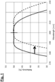
- the aforementioned laser light sources which changes - as indicated in the merely exemplary diagram of Figure 13 - ultimately correspond in terms of their effect on the reflection or transmission behaviour to a shift of the effective wavelength of the electromagnetic radiation incident on the relevant component.
- the optical component which as a rule is designed for the respective operating wavelength of the optical system (e.g., 193 nm), then no longer exhibits its optimal behaviour in the case of this shift of the effective wavelength, with the result that the performance of the optical system is also impaired, wherein, for instance in the aforementioned example of the laser light source, the respectively provided source power is subjected to unwanted fluctuations.
- an optical component comprises:
- the invention is based on the concept of designing the respective wavelength-dependent reflectivity curves of layer systems present on different optical surfaces of a component in such a way that, even in the case of a drift of the respective reflectivity behaviour of the relevant layer systems, which is caused for example by the surroundings of the component and in particular by contamination or degradation, the resultant summated reflectivity behaviour of the optical component remains at least largely constant or at least only deviates slightly from a desired linear reflectivity curve with respect to the wavelength.
- the present invention takes the approach of matching the layer systems situated on at least two optical surfaces of a component to one another, in such a way that the respective wavelength-dependent reflectivity curves - which are consciously allowed for each individual relevant layer system - at least partially compensate one another with the result that, for the totality of the relevant layer systems or the respective optical component, a spectral drift in the reflection behaviour, which is problematic in view of the performance of the optical system, no longer occurs or only still occurs to a small extent.
- a constant operating wavelength e.g., a laser light source
- the reflectivity of the second layer system may also equal zero, in the case of which the resultant reflectivity within the specified wavelength range corresponds to the reflectivity of the first layer system.
- the wavelength dependencies of the first and the second reflectivity curve at least partially compensate one another in such a way that the relative deviation from a desired reflectivity curve which is linear or constant with respect to the wavelength is no more than 3%, in particular no more than 2% within the specified wavelength range for a resultant summated reflectivity for the first layer system and the at least one second layer system.
- a resultant summated reflectivity for the first layer system and the at least one second layer system is constant within the specified wavelength range apart from a maximum relative variation of 5%, in particular apart from a maximum relative variation of 3%, more particularly apart from a maximum relative variation of 2%.
- a maximum variation of the reflectivity for the resultant reflectivity curve within the specified wavelength range is less than the respective maximum variation of the reflectivity, within the specified wavelength range, for the first wavelength-dependent reflectivity curve and for the second wavelength-dependent reflectivity curve.
- the reflectivity as a function of the wavelength, within the specified wavelength range varies by at least 5%, in particular by at least 10% in relation to the maximum reflectivity according to an embodiment.
- the optical component further comprises at least one third layer system with a third wavelength-dependent reflectivity curve.
- the relative deviation within the specified wavelength range from a desired linear reflectivity curve is no more than 5%, in particular no more than 3%, more particularly no more than 2% according to an embodiment.
- the specified wavelength range extends for a given operating wavelength ⁇ 0 from 0.95 ⁇ 0 to 1.05 ⁇ 0 , in particular from 0.9 ⁇ 0 to 1.1 ⁇ 0 , more particularly from 0.8 ⁇ 0 to 1.2 ⁇ 0 , and more particularly from 0.7 ⁇ 0 to 1.3 ⁇ 0 .
- the optical component comprises at least one beam splitter.
- the optical component comprises an output coupling element for output coupling a component beam from the optical beam path of an optical system.
- the optical component comprises a deflection element for deflecting a component beam in the optical beam path of an optical system.
- the optical component is designed for an operating wavelength ranging from 100 nm to 700 nm.
- the invention also relates to an optical system, in particular for microlithography, comprising an optical component in accordance with the above-described features.
- the optical component can be arranged within a laser light source (without however the invention being restricted thereto).
- the present invention in particular proceeds from the idea that - as already explained at the outset on the basis of the diagram in Figure 13 - a degradation in the material of an optical component such as a beam splitter, for example, ultimately corresponds in terms of its effect on the reflection behaviour of the optical component to a shift of the effective wavelength which, without suitable countermeasures, is accompanied by an impairment of the performance of the relevant optical component (which of course was initially constructed in a targeted manner for the specific operating wavelength of the respective optical system).
- an allowance is made for these circumstances by virtue of a substantially plateau-shaped wavelength-dependent reflectivity curve for the component overall being sought after for the relevant optical component even over a relatively large wavelength range - despite its intended use only for a specific operating wavelength (of 193 nm, for example) - since, as indicated in Figure 1 , a consequence of this plateau-shaped curve is that the aforementioned degradation-related shift of the effective wavelength no longer leads to an impairment in the optical reflection behaviour.
- the substantially constant performance of the optical component in view of the reflection behaviour is achieved overall according to the invention by virtue of at least two layer systems situated on different surfaces of the optical component having in a certain sense opposing wavelength-dependent reflectivity curves and consequently being "pitted against one another" in respect of their respective degradation effect or being matched to one another within the meaning of a mutual compensation.
- the concept according to the invention can be realized in an optical component in the form of an optical beam splitter, for example as is used in a laser light source or in other optical systems, especially for microlithography.
- a beam splitter 200 can be constructed from a first layer system 210 and a second layer system 220, with Figure 2 further indicating, for an incident light beam with the intensity I 0 , the occurrence of both a reflected intensity component I R and a transmitted intensity component I T .
- r 1 and r 2 denote the respective partial reflectivities of the first and the second layer system 210, 220.
- Figure 3a now shows a possible wavelength-dependent reflectivity curve for the first layer system 210
- Figure 3b shows a wavelength-dependent reflectivity curve for the second layer system 220 suitable according to the invention for obtaining the desired compensation effect.
- Figures 3a-3b significant variations of the individual wavelength-dependent reflectivity curves are definitely "allowed" in the process, with however these wavelength-dependent variations (including the intermediate extremals present in the specific example) running precisely counter or complementary to one another.
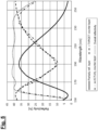
- Figure 4 shows a further example for the matching to one another according to the invention of two layer systems of an optical component such as an optical beam splitter, for example, with the reflectivity curve (illustrated using dashed lines) of the second layer system once again running precisely counter to the reflectivity curve (illustrated using a solid line) of the first layer system.
- an optical component such as an optical beam splitter
- Table 1 shows a possible layer design for a first layer system
- Table 2 shows a suitable layer design of a second layer system suitable for obtaining the desired compensation effect.
- Table 1 Material Layer thickness [ ⁇ /4] LaF 3 1 MgF 2 1 LaF 3 1 MgF 2 1 LaF 3 1
- Table 2 Material Layer thickness [ ⁇ /4] LaF 3 1.82 MgF 2 1.54 LaF 3 1.69 MgF 2 0.99 LaF 3 1.01 MgF 2 1.85 LaF 3 1.05 MgF 2 1.02 LaF 3 0.99
- Figure 5 shows the corresponding wavelength-dependent reflectivity curves, with both the desired target profile for an ideal compensation effect and the actual profile in fact realized by the specific layer design being illustrated for the second layer system.
- a largely plateau-shaped curve over a comparatively broad wavelength range from approximately 160 nm to 240 nm is achieved for the resultant overall reflectivity.
- Table 3 shows a further possible layer design of a first layer system
- Table 4 shows a layer design of a correspondingly matched second layer system suitable for obtaining the compensation effect according to the invention.
- Table 3 Material Layer thickness [ ⁇ /4] LaF 3 1 MgF 2 2 LaF 3 1 MgF 2 1 LaF 3 1 MgF 2 1 LaF 3 1.1
- Table 4 Material Layer thickness [ ⁇ /4] LaF 3 0.31 MgF 2 1.25 LaF 3 1.02 MgF 2 1.99 LaF 3 0.99 MgF 2 1.68 LaF 3 1.43
- Figure 6 shows the respective wavelength-dependent reflectivity curves for the exemplary embodiment of Table 3 to Table 4.
- FIG. 7 shows, only in a schematic illustration, an optical component 700 made up of two partial components 701, 702, with the partial component 701 yet again being an optical beam splitter and the partial component 702 being a mirror. Consequently, a total of three optically effective surfaces or layer systems 710, 720, 730 present at these surfaces are available for the component 700, which surfaces or layer systems can be matched to one another in respect of their respective wavelength-dependent reflectivity curves for the purpose of obtaining the compensation effect according to the invention.
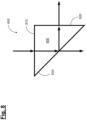
- Figure 8 shows, as a further application example, an optical component 800 with three optically effective surfaces or layer systems 810, 820, 830 situated thereon.
- the optical component 800 selectively acts as a deflection mirror (for the portion reflected at the layer system 830 and transmitted through the layer system 820) or as an output coupling element (for the portion transmitted through the layer system 830).
- the layer systems 820 and 830 can be matched to one another according to the invention in such a way that the ratio of the portions transmitted there in each case remains constant over a sufficiently broad wavelength range.
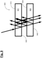
- Figure 9 shows a further example of an optical component 900 which is made up of two partial components 901, 902, each in the form of a beam splitter. Consequently, a total of four optically effective surfaces or layer systems 910, 920, 930 and 940 situated thereon are available for the purpose of obtaining the compensation effect according to the invention.
- Figure 10 shows an optical component 1000 in the form of a deflection or output coupling element, wherein three different optical surfaces or layer systems 1010, 1020, 1030 situated thereon are available, of which however the layer system 1010 is passed through twice in accordance with the indicated beam path.
- the optical component 1000 can be used to output couple two different component beams (corresponding to the portion transmitted through the layer system 1020 and the portion transmitted through the layer system 1030).
- all three layer systems or else only two of these layer systems can be matched to one another, in the manner according to the invention, in respect of their wavelength-dependent reflectivity curve.
- Figure 11 shows a structure, possible in principle, of a microlithographic projection exposure apparatus 1100 designed for operation in the DUV.
- the projection exposure apparatus 1100 in accordance with Figure 11 comprises an illumination device 1110 and a projection lens 1120.
- the illumination device 1110 serves for illuminating a structure-bearing mask (reticle) 1115 with light from a light source unit 1105 comprising a laser light source for example in the form of an ArF excimer laser for an operating wavelength of 193 nm (or else in the form of a KrF excimer laser for an operating wavelength of 248 nm) and also a beam shaping optical unit that generates a parallel light beam.
- the laser light source can be designed in the manner according to the invention.
- the illumination device 1110 comprises an optical unit 1111 which, inter alia, comprises a deflection mirror 1112 in the example illustrated.
- the optical unit 1111 can comprise for example a diffractive optical element (DOE) and a zoom-axicon system for producing different illumination settings (i.e., intensity distributions in a pupil plane of the illumination device 1110).
- DOE diffractive optical element
- zoom-axicon system for producing different illumination settings (i.e., intensity distributions in a pupil plane of the illumination device 1110).
- a light mixing device (not illustrated) is situated in the beam path downstream of the optical unit 1111 in the light propagation direction, which light mixing device can have for example, in a manner known per se, an arrangement composed of micro-optical elements which is suitable for attaining light mixing, and a lens-element group 1113, downstream of which there is a field plane with a reticle masking system (REMA), which is imaged by a REMA lens 1114, disposed downstream in the light propagation direction, onto the structure-bearing mask (reticle) 1115 arranged in a further field plane and which thereby delimits the illuminated region on the reticle.
- a reticle masking system REMA lens
- the structure-bearing mask 1115 is imaged onto a substrate provided with a light-sensitive layer (photoresist) or onto a wafer 1130.
- the projection lens 1120 can be designed for immersion operation, in which case an immersion medium is situated upstream of the wafer, or the light-sensitive layer thereof, in relation to the light propagation direction.
- it can have for example a numerical aperture NA greater than 0.85, in particular greater than 1.1.
- Figure 12a indicates, purely schematically, a laser 1210 having a beam splitter 1211 inserted therein as an exemplary application of the present invention.
- beam splitters may also be used in an optical pulse stretcher or else for the purpose of output coupling a component beam, for example for beam measurement purposes.
- Figure 12b indicates, likewise purely schematically, a microscope 1220 (e.g., for wafer inspection) having a beam splitter 1221 inserted therein as a further exemplary application of the invention.
Landscapes
- Physics & Mathematics (AREA)
- General Physics & Mathematics (AREA)
- Optics & Photonics (AREA)
- Optical Elements Other Than Lenses (AREA)
- Exposure And Positioning Against Photoresist Photosensitive Materials (AREA)
Abstract
Description
- This application claims priority of German
Patent Application DE 10 2022 113 164.5 filed on May 24, 2022 . The content of this application is hereby incorporated by reference. - The invention relates to an optical component and an optical system. The invention is advantageously applicable in a laser light source, for example, but also in other applications, and in particular it can be used in a microlithographic projection exposure apparatus.
- Microlithography is used to produce microstructured, electronic components. The microlithography process is carried out in what is known as a projection exposure apparatus, which has an illumination device and a projection lens. The image of a mask (= reticle) illuminated by means of the illumination device is projected in this case by means of the projection lens onto a substrate (for example a silicon wafer) that is coated with a light-sensitive layer (photoresist) and arranged in the image plane of the projection lens in order to transfer the mask structure to the light-sensitive coating of the substrate.
- In a projection exposure apparatus designed for operation in the DUV range (e.g., at operating wavelengths of less than 250 nm, in particular less than 200 nm), use is typically made of laser light sources in the form of excimer lasers, in particular krypton fluoride excimer lasers at an operating wavelength of 248 nm or argon fluoride excimer lasers at an operating wavelength of 193 nm.
- Existing challenges within the scope of the development of projection exposure apparatuses relate, inter alia, to ever more stringent requirements in respect of accuracy for the microlithographic production of ever smaller structures and the positioning thereof on the wafer.
- A problem arising in optical components, for example in the aforementioned laser light sources but also in the illumination device, in the projection lens or in other optical systems, is that degradation in the material of the components caused by the respective ambient conditions (e.g., by being bombarded with electromagnetic radiation, ions, etc.) leads to changes in the respective optical properties which, in turn, are accompanied by an impairment of the performance of the optical system comprising the relevant component.
- For instance, depending on the ambient conditions, unwanted changes in the wavelength-dependent reflection or transmission curve arise in beam splitters used in optical systems such as, for example, the aforementioned laser light sources, which changes - as indicated in the merely exemplary diagram of
Figure 13 - ultimately correspond in terms of their effect on the reflection or transmission behaviour to a shift of the effective wavelength of the electromagnetic radiation incident on the relevant component. The optical component, which as a rule is designed for the respective operating wavelength of the optical system (e.g., 193 nm), then no longer exhibits its optimal behaviour in the case of this shift of the effective wavelength, with the result that the performance of the optical system is also impaired, wherein, for instance in the aforementioned example of the laser light source, the respectively provided source power is subjected to unwanted fluctuations. - Regarding the prior art, reference is only made by way of example to
EP 3 111 257 B1 . - It is an object of the present invention to provide an optical component and an optical system which enable operation that is as stable as possible even under varying use conditions while avoiding the problems described above to at least some extent.
- This object is achieved by means of the optical component in accordance with the features of
independent patent Claim 1 and the optical system in accordance with the features of alternative independent patent Claim 13. - According to the invention, an optical component comprises:
- a first layer system which exhibits a first wavelength-dependent reflectivity curve when electromagnetic radiation impinges thereon; and
- at least one second layer system which exhibits a second wavelength-dependent reflectivity curve when electromagnetic radiation impinges thereon;
- wherein the first layer system and the second layer system are arranged on different optical surfaces; and
- wherein the wavelength dependencies of the first and the second reflectivity curve at least partially compensate one another in such a way that the relative deviation from a desired reflectivity curve which is linear or constant with respect to the wavelength is no more than 5% within the specified wavelength range for a resultant summated reflectivity for the first layer system and the at least one second layer system.
- In particular, the invention is based on the concept of designing the respective wavelength-dependent reflectivity curves of layer systems present on different optical surfaces of a component in such a way that, even in the case of a drift of the respective reflectivity behaviour of the relevant layer systems, which is caused for example by the surroundings of the component and in particular by contamination or degradation, the resultant summated reflectivity behaviour of the optical component remains at least largely constant or at least only deviates slightly from a desired linear reflectivity curve with respect to the wavelength.
- In other words, the present invention takes the approach of matching the layer systems situated on at least two optical surfaces of a component to one another, in such a way that the respective wavelength-dependent reflectivity curves - which are consciously allowed for each individual relevant layer system - at least partially compensate one another with the result that, for the totality of the relevant layer systems or the respective optical component, a spectral drift in the reflection behaviour, which is problematic in view of the performance of the optical system, no longer occurs or only still occurs to a small extent.
- By virtue of the invention allowing deliberate reversible structural changes and, accompanying these, spectral shifts in the reflection behaviour for each individual layer system of the aforementioned layer systems, it is possible as a result to ensure a stable and largely constant operation at all times even in the case of ambient conditions which are comparatively problematic in view of the risk of degradation or contamination (e.g., in the wavelength range from 100 nm to 700 nm, in particular from 100 nm to 400 nm, on account of the comparatively highly energetic electromagnetic radiation and the optionally present atmosphere in the respective optical system) and especially also in the case of fluctuations in these ambient conditions over time, since, as described above, the relevant layer systems are in a certain sense "pitted" against one another in view of the effects of the said changes during operation.
- According to the invention, the disadvantage of increased outlay for the construction of the respective layer design on different surfaces of the optical component in view of mutual compensation in relation to the respective wavelength-dependent reflectivity curve even in the case of an optical system with in actual fact a constant operating wavelength (e.g., a laser light source) is consciously accepted since, in return, this construction can account for the effects of degradation or reversible structural changes within the meaning of the shift of the effective wavelength in the reflection behaviour described at the outset.
- The reflectivity of the second layer system may also equal zero, in the case of which the resultant reflectivity within the specified wavelength range corresponds to the reflectivity of the first layer system.
- According to an embodiment the wavelength dependencies of the first and the second reflectivity curve at least partially compensate one another in such a way that the relative deviation from a desired reflectivity curve which is linear or constant with respect to the wavelength is no more than 3%, in particular no more than 2% within the specified wavelength range for a resultant summated reflectivity for the first layer system and the at least one second layer system.
- According to an embodiment, a resultant summated reflectivity for the first layer system and the at least one second layer system is constant within the specified wavelength range apart from a maximum relative variation of 5%, in particular apart from a maximum relative variation of 3%, more particularly apart from a maximum relative variation of 2%.
- According to an embodiment, a maximum variation of the reflectivity for the resultant reflectivity curve within the specified wavelength range is less than the respective maximum variation of the reflectivity, within the specified wavelength range, for the first wavelength-dependent reflectivity curve and for the second wavelength-dependent reflectivity curve.
- In the first reflectivity curve of the first layer system, the reflectivity as a function of the wavelength, within the specified wavelength range, varies by at least 5%, in particular by at least 10% in relation to the maximum reflectivity according to an embodiment.
- According to an embodiment, the optical component further comprises at least one third layer system with a third wavelength-dependent reflectivity curve.
- For a resultant summated reflectivity for the first layer system, the second layer system and the third layer system, the relative deviation within the specified wavelength range from a desired linear reflectivity curve is no more than 5%, in particular no more than 3%, more particularly no more than 2% according to an embodiment.
- According to an embodiment, the specified wavelength range extends for a given operating wavelength λ0 from 0.95∗λ0 to 1.05∗λ0, in particular from 0.9∗λ0 to 1.1∗λ0, more particularly from 0.8∗λ0 to 1.2∗λ0, and more particularly from 0.7∗λ0 to 1.3∗λ0.
- According to an embodiment, the optical component comprises at least one beam splitter.
- According to an embodiment, the optical component comprises an output coupling element for output coupling a component beam from the optical beam path of an optical system.
- According to an embodiment, the optical component comprises a deflection element for deflecting a component beam in the optical beam path of an optical system.
- According to an embodiment, the optical component is designed for an operating wavelength ranging from 100 nm to 700 nm.
- Further, the invention also relates to an optical system, in particular for microlithography, comprising an optical component in accordance with the above-described features. In particular, the optical component can be arranged within a laser light source (without however the invention being restricted thereto).
- Further embodiments of the invention are evident from the description and the dependent claims.
- The invention will be explained in greater detail below on the basis of an exemplary embodiment that is illustrated in the accompanying figures.
- In the figures:
- Figure 1
- shows a diagram for explaining a concept underlying the present invention;
- Figure 2
- shows a schematic illustration of the basic possible structure of a beam splitter in which the present invention can be realized;
- Figures 3a-6
- show diagrams for explaining possible embodiments of the present invention;
- Figures 7-10
- show schematic illustrations of exemplary optical components in which the present invention can be realized;
- Figure 11
- shows a schematic illustration for explaining the possible structure of a microlithographic projection exposure apparatus designed for operation in the DUV;
- Figures 12a-12b
- show schematic illustrations of exemplary applications of the invention; and
- Figure 13
- shows a diagram for explaining a problem occurring in accordance with the prior art.
- Embodiments of the present invention are explained hereinafter with reference to the diagrams in
Figures 3a-6 and also the schematic illustrations inFigure 2 andFigures 7-10 . - What is common to the embodiments described hereinafter is that - in view of the object of avoiding a change in the optical performance occurring due to a degradation during operation of an optical component or an optical system comprising this component - at least two layer systems situated on different surfaces of the relevant optical component are matched to one another in terms of their respective wavelength-dependent reflectivity behaviour so that, in respect of the effects of a degradation or structural change, an at least partial compensation effect and, overall, a largely constant reflectivity behaviour of the optical component are obtained.
- In so doing, the present invention in particular proceeds from the idea that - as already explained at the outset on the basis of the diagram in
Figure 13 - a degradation in the material of an optical component such as a beam splitter, for example, ultimately corresponds in terms of its effect on the reflection behaviour of the optical component to a shift of the effective wavelength which, without suitable countermeasures, is accompanied by an impairment of the performance of the relevant optical component (which of course was initially constructed in a targeted manner for the specific operating wavelength of the respective optical system). According to the invention, an allowance is made for these circumstances by virtue of a substantially plateau-shaped wavelength-dependent reflectivity curve for the component overall being sought after for the relevant optical component even over a relatively large wavelength range - despite its intended use only for a specific operating wavelength (of 193 nm, for example) - since, as indicated inFigure 1 , a consequence of this plateau-shaped curve is that the aforementioned degradation-related shift of the effective wavelength no longer leads to an impairment in the optical reflection behaviour. - As described below on the basis of various embodiments with reference to
Figure 2 toFigure 10 , the substantially constant performance of the optical component in view of the reflection behaviour is achieved overall according to the invention by virtue of at least two layer systems situated on different surfaces of the optical component having in a certain sense opposing wavelength-dependent reflectivity curves and consequently being "pitted against one another" in respect of their respective degradation effect or being matched to one another within the meaning of a mutual compensation. - In particular (but without the invention being restricted thereto), the concept according to the invention can be realized in an optical component in the form of an optical beam splitter, for example as is used in a laser light source or in other optical systems, especially for microlithography. According to the purely schematic illustration in
Figure 2 , such abeam splitter 200 can be constructed from afirst layer system 210 and asecond layer system 220, withFigure 2 further indicating, for an incident light beam with the intensity I0, the occurrence of both a reflected intensity component IR and a transmitted intensity component IT. Both the overall reflectivity resulting for thebeam splitter 200 and the corresponding overall transmissivity are composed of the respective properties of the twolayer systems 
second layer system - For the exemplary realization of the concept according to the invention,
Figure 3a now shows a possible wavelength-dependent reflectivity curve for thefirst layer system 210, andFigure 3b shows a wavelength-dependent reflectivity curve for thesecond layer system 220 suitable according to the invention for obtaining the desired compensation effect. As is evident fromFigures 3a-3b , significant variations of the individual wavelength-dependent reflectivity curves are definitely "allowed" in the process, with however these wavelength-dependent variations (including the intermediate extremals present in the specific example) running precisely counter or complementary to one another. -
Figure 4 shows a further example for the matching to one another according to the invention of two layer systems of an optical component such as an optical beam splitter, for example, with the reflectivity curve (illustrated using dashed lines) of the second layer system once again running precisely counter to the reflectivity curve (illustrated using a solid line) of the first layer system. - To illustrate a specific exemplary embodiment, Table 1 shows a possible layer design for a first layer system, and Table 2 shows a suitable layer design of a second layer system suitable for obtaining the desired compensation effect.
Table 1: Material Layer thickness [λ/4] LaF3 1 MgF 21 LaF 31 MgF 21 LaF 31 Table 2: Material Layer thickness [λ/4] LaF3 1.82 MgF2 1.54 LaF3 1.69 MgF2 0.99 LaF3 1.01 MgF2 1.85 LaF3 1.05 MgF2 1.02 LaF3 0.99 - In this respect,
Figure 5 shows the corresponding wavelength-dependent reflectivity curves, with both the desired target profile for an ideal compensation effect and the actual profile in fact realized by the specific layer design being illustrated for the second layer system. As is evident fromFigure 5 , a largely plateau-shaped curve over a comparatively broad wavelength range from approximately 160 nm to 240 nm is achieved for the resultant overall reflectivity. - As a further specific exemplary embodiment, Table 3 shows a further possible layer design of a first layer system, and Table 4 shows a layer design of a correspondingly matched second layer system suitable for obtaining the compensation effect according to the invention.
Table 3: Material Layer thickness [λ/4] LaF3 1 MgF 22 LaF 31 MgF 21 LaF 31 MgF 21 LaF3 1.1 Table 4: Material Layer thickness [λ/4] LaF3 0.31 MgF2 1.25 LaF3 1.02 MgF2 1.99 LaF3 0.99 MgF2 1.68 LaF3 1.43 - In a manner analogous to
Figure 5 ,Figure 6 shows the respective wavelength-dependent reflectivity curves for the exemplary embodiment of Table 3 to Table 4. - The invention is not restricted to the realization with two mutually matched layer systems on an optical component.
Figure 7 shows, only in a schematic illustration, anoptical component 700 made up of twopartial components partial component 701 yet again being an optical beam splitter and thepartial component 702 being a mirror. Consequently, a total of three optically effective surfaces orlayer systems component 700, which surfaces or layer systems can be matched to one another in respect of their respective wavelength-dependent reflectivity curves for the purpose of obtaining the compensation effect according to the invention. -
Figure 8 shows, as a further application example, anoptical component 800 with three optically effective surfaces orlayer systems optical component 800 selectively acts as a deflection mirror (for the portion reflected at thelayer system 830 and transmitted through the layer system 820) or as an output coupling element (for the portion transmitted through the layer system 830). In this case, depending on the specific use scenario, thelayer systems - In a schematic illustration,
Figure 9 shows a further example of anoptical component 900 which is made up of twopartial components layer systems - As a further possible exemplary application,
Figure 10 shows anoptical component 1000 in the form of a deflection or output coupling element, wherein three different optical surfaces orlayer systems layer system 1010 is passed through twice in accordance with the indicated beam path. As indicated inFigure 10 , theoptical component 1000 can be used to output couple two different component beams (corresponding to the portion transmitted through thelayer system 1020 and the portion transmitted through the layer system 1030). Moreover, depending on the specific use scenario, all three layer systems or else only two of these layer systems can be matched to one another, in the manner according to the invention, in respect of their wavelength-dependent reflectivity curve. -
Figure 11 shows a structure, possible in principle, of a microlithographicprojection exposure apparatus 1100 designed for operation in the DUV. - The
projection exposure apparatus 1100 in accordance withFigure 11 comprises anillumination device 1110 and aprojection lens 1120. Theillumination device 1110 serves for illuminating a structure-bearing mask (reticle) 1115 with light from alight source unit 1105 comprising a laser light source for example in the form of an ArF excimer laser for an operating wavelength of 193 nm (or else in the form of a KrF excimer laser for an operating wavelength of 248 nm) and also a beam shaping optical unit that generates a parallel light beam. In this case, the laser light source can be designed in the manner according to the invention. - The
illumination device 1110 comprises anoptical unit 1111 which, inter alia, comprises adeflection mirror 1112 in the example illustrated. Theoptical unit 1111 can comprise for example a diffractive optical element (DOE) and a zoom-axicon system for producing different illumination settings (i.e., intensity distributions in a pupil plane of the illumination device 1110). A light mixing device (not illustrated) is situated in the beam path downstream of theoptical unit 1111 in the light propagation direction, which light mixing device can have for example, in a manner known per se, an arrangement composed of micro-optical elements which is suitable for attaining light mixing, and a lens-element group 1113, downstream of which there is a field plane with a reticle masking system (REMA), which is imaged by aREMA lens 1114, disposed downstream in the light propagation direction, onto the structure-bearing mask (reticle) 1115 arranged in a further field plane and which thereby delimits the illuminated region on the reticle. By means of theprojection lens 1120, the structure-bearingmask 1115 is imaged onto a substrate provided with a light-sensitive layer (photoresist) or onto awafer 1130. In particular, theprojection lens 1120 can be designed for immersion operation, in which case an immersion medium is situated upstream of the wafer, or the light-sensitive layer thereof, in relation to the light propagation direction. Furthermore, it can have for example a numerical aperture NA greater than 0.85, in particular greater than 1.1. -
Figure 12a indicates, purely schematically, alaser 1210 having abeam splitter 1211 inserted therein as an exemplary application of the present invention. By way of example, beam splitters may also be used in an optical pulse stretcher or else for the purpose of output coupling a component beam, for example for beam measurement purposes.Figure 12b indicates, likewise purely schematically, a microscope 1220 (e.g., for wafer inspection) having abeam splitter 1221 inserted therein as a further exemplary application of the invention. - Even though the invention has also been described on the basis of specific embodiments, numerous variations and alternative embodiments will be apparent to a person skilled in the art, for example by the combination and/or exchange of features of individual embodiments. Accordingly, it goes without saying for a person skilled in the art that such variations and alternative embodiments are concomitantly encompassed by the present invention, and the scope of the invention is restricted only within the meaning of the appended patent claims and the equivalents thereof.
Claims (14)
- Optical component, comprising:• a first layer system (210, 710, 810, 910, 1010) which exhibits a first wavelength-dependent reflectivity curve when electromagnetic radiation impinges thereon; and• at least one second layer system (220, 720, 820, 920, 1020) which exhibits a second wavelength-dependent reflectivity curve when electromagnetic radiation impinges thereon;• wherein the first layer system (210, 710, 810, 910, 1010) and the second layer system (220, 720, 820, 920, 1020) are arranged on different optical surfaces; and• wherein the wavelength dependencies of the first and the second reflectivity curve at least partially compensate one another in such a way that the relative deviation from a desired reflectivity curve which is linear or constant with respect to the wavelength is no more than 5% within the specified wavelength range for a resultant summated reflectivity for the first layer system (210, 710, 810, 910, 1010) and the at least one second layer system (220, 720, 820, 920, 1020).
- Optical component according to Claim 1, characterized in that the wavelength dependencies of the first and the second reflectivity curve at least partially compensate one another in such a way that the relative deviation from a desired reflectivity curve which is linear or constant with respect to the wavelength is no more than 3%, in particular no more than 2% within the specified wavelength range for a resultant summated reflectivity for the first layer system (210, 710, 810, 910, 1010) and the at least one second layer system (220, 720, 820, 920, 1020).
- Optical component according to Claim 1 or 2, characterized in that a resultant summated reflectivity for the first layer system (210, 710, 810, 910, 1010) and the at least one second layer system (220, 720, 820, 920, 1020) is constant within the specified wavelength range apart from a maximum relative variation of 5%, in particular apart from a maximum relative variation of 3%, more particularly apart from a maximum relative variation of 2%.
- Optical component according to any of Claims 1 to 3, characterized in that a maximum variation of the reflectivity for the resultant reflectivity curve within the specified wavelength range is less than the respective maximum variation of the reflectivity, within the specified wavelength range, for the first wavelength-dependent reflectivity curve and for the second wavelength-dependent reflectivity curve.
- Optical component according to any of the preceding claims, characterized in that, in the first reflectivity curve of the first layer system (210, 710, 810, 910, 1010), the reflectivity as a function of the wavelength, within the specified wavelength range, varies by at least 5%, in particular by at least 10% in relation to the maximum reflectivity.
- Optical component according to any of the preceding claims, characterized in that the said optical component further comprises at least one third layer system (730, 830, 930, 1030) with a third wavelength-dependent reflectivity curve.
- Optical component according to Claim 6, characterized in that for a resultant summated reflectivity for the first layer system (710, 810, 910, 1010), the second layer system (720, 820, 920, 1020) and the third layer system (730, 830, 930, 1030), the relative deviation within the specified wavelength range from a desired linear reflectivity curve is no more than 5%, in particular no more than 3%, more particularly no more than 2%.
- Optical component according to any of the preceding claims, characterized in that the specified wavelength range extends for a given operating wavelength λ0 from 0.95∗λ0 to 1.05∗λ0, in particular from 0.9∗λ0 to 1.1∗λ0, more particularly from 0.8∗λ0 to 1.2∗λ0, and more particularly from 0.7∗λ0 to 1.3∗λ0.
- Optical component according to any of the preceding claims, characterized in that the said optical component comprises at least one beam splitter.
- Optical component according to any of the preceding claims, characterized in that the said optical component comprises an output coupling element for output coupling a component beam from the optical beam path of an optical system.
- Optical component according to any of the preceding claims, characterized in that the said optical component comprises a deflection element for deflecting a component beam in the optical beam path of an optical system.
- Optical component according to any of the preceding claims, characterized in that the said optical component is designed for an operating wavelength ranging from 100 nm to 700 nm.
- Optical system, in particular for microlithography, comprising an optical component according to any of the preceding claims.
- Optical system according to Claim 13, characterized in that the optical component is arranged within a laser light source.
Applications Claiming Priority (1)
| Application Number | Priority Date | Filing Date | Title |
|---|---|---|---|
| DE102022113164.5A DE102022113164B4 (en) | 2022-05-24 | 2022-05-24 | Optical component and optical system, especially for microlithography |
Publications (1)
| Publication Number | Publication Date |
|---|---|
| EP4283349A1 true EP4283349A1 (en) | 2023-11-29 |
Family
ID=86331152
Family Applications (1)
| Application Number | Title | Priority Date | Filing Date |
|---|---|---|---|
| EP23172459.2A Pending EP4283349A1 (en) | 2022-05-24 | 2023-05-09 | Optical component and optical system, in particular for microlithography |
Country Status (5)
| Country | Link |
|---|---|
| US (1) | US12468230B2 (en) |
| EP (1) | EP4283349A1 (en) |
| JP (2) | JP2023182537A (en) |
| CN (1) | CN117111188A (en) |
| DE (1) | DE102022113164B4 (en) |
Cited By (1)
| Publication number | Priority date | Publication date | Assignee | Title |
|---|---|---|---|---|
| WO2026052255A1 (en) * | 2024-09-09 | 2026-03-12 | Carl Zeiss Smt Gmbh | Optical element having a coating, optical arrangement and method of producing an optical element |
Citations (3)
| Publication number | Priority date | Publication date | Assignee | Title |
|---|---|---|---|---|
| DE10248707A1 (en) * | 2002-10-18 | 2004-05-13 | Tuilaser Ag | Highly reflective mirror for an excimer laser comprises a substrate, a first highly reflective layer system formed on the inner side of the substrate, and a second highly reflective layer system formed on the outer side of the substrate |
| US20120224265A1 (en) * | 2011-03-03 | 2012-09-06 | Clark Stephan R | Supporting a substrate within an optical component |
| US20130250405A1 (en) * | 2011-10-20 | 2013-09-26 | 3M Innovative Properties Company | Multilayer stack combinations with interleaved overlapping harmonics for wide visible-infrared coverage |
Family Cites Families (6)
| Publication number | Priority date | Publication date | Assignee | Title |
|---|---|---|---|---|
| JP2005189395A (en) | 2003-12-25 | 2005-07-14 | Nikon Corp | Transmission type dispersion compensation filter |
| US20080266651A1 (en) | 2007-04-24 | 2008-10-30 | Katsuhiko Murakami | Optical apparatus, multilayer-film reflective mirror, exposure apparatus, and device |
| DE102010060558B3 (en) | 2010-11-15 | 2012-03-29 | Leica Microsystems Cms Gmbh | Optic element has beam splitter layer whose reflected exit light beam, and compensation layer arrangements whose transmitted exit light beam, are within predetermined wavelength range agreeing spectral energy distributions |
| JP6093753B2 (en) * | 2011-03-23 | 2017-03-08 | カール・ツァイス・エスエムティー・ゲーエムベーハー | EUV mirror mechanism, optical system with EUV mirror mechanism, and method of operating an optical system with EUV mirror mechanism |
| US10295707B2 (en) | 2014-02-27 | 2019-05-21 | Corning Incorporated | Durability coating for oxide films for metal fluoride optics |
| US11269901B2 (en) | 2020-01-16 | 2022-03-08 | International Business Machines Corporation | Cognitive test advisor facility for identifying test repair actions |
-
2022
- 2022-05-24 DE DE102022113164.5A patent/DE102022113164B4/en active Active
-
2023
- 2023-05-09 EP EP23172459.2A patent/EP4283349A1/en active Pending
- 2023-05-22 US US18/321,244 patent/US12468230B2/en active Active
- 2023-05-23 CN CN202310586839.7A patent/CN117111188A/en active Pending
- 2023-05-24 JP JP2023085155A patent/JP2023182537A/en active Pending
-
2025
- 2025-08-14 JP JP2025135044A patent/JP2026009870A/en active Pending
Patent Citations (3)
| Publication number | Priority date | Publication date | Assignee | Title |
|---|---|---|---|---|
| DE10248707A1 (en) * | 2002-10-18 | 2004-05-13 | Tuilaser Ag | Highly reflective mirror for an excimer laser comprises a substrate, a first highly reflective layer system formed on the inner side of the substrate, and a second highly reflective layer system formed on the outer side of the substrate |
| US20120224265A1 (en) * | 2011-03-03 | 2012-09-06 | Clark Stephan R | Supporting a substrate within an optical component |
| US20130250405A1 (en) * | 2011-10-20 | 2013-09-26 | 3M Innovative Properties Company | Multilayer stack combinations with interleaved overlapping harmonics for wide visible-infrared coverage |
Cited By (1)
| Publication number | Priority date | Publication date | Assignee | Title |
|---|---|---|---|---|
| WO2026052255A1 (en) * | 2024-09-09 | 2026-03-12 | Carl Zeiss Smt Gmbh | Optical element having a coating, optical arrangement and method of producing an optical element |
Also Published As
| Publication number | Publication date |
|---|---|
| US20230384687A1 (en) | 2023-11-30 |
| CN117111188A (en) | 2023-11-24 |
| DE102022113164B4 (en) | 2025-07-10 |
| DE102022113164A1 (en) | 2023-11-30 |
| US12468230B2 (en) | 2025-11-11 |
| JP2023182537A (en) | 2023-12-26 |
| JP2026009870A (en) | 2026-01-21 |
Similar Documents
| Publication | Publication Date | Title |
|---|---|---|
| US5789734A (en) | Exposure apparatus that compensates for spherical aberration of an image forming device | |
| US8451430B2 (en) | Illumination optical system, exposure apparatus, and device manufacturing method | |
| KR20060120629A (en) | Exposure method and apparatus, and device manufacturing method | |
| US5796524A (en) | Catadioptric optical system and exposure apparatus using the same | |
| EP1293834A2 (en) | Illumination apparatus | |
| EP1865362B1 (en) | Reflective loop system producing incoherent radiation | |
| JP3605047B2 (en) | Illumination apparatus, exposure apparatus, device manufacturing method and device | |
| JP3762323B2 (en) | Exposure equipment | |
| US12468230B2 (en) | Optical component and optical system, in particular for microlithography | |
| US8947635B2 (en) | Illumination optical system, exposure apparatus, and device manufacturing method | |
| US8164739B2 (en) | Controlling fluctuations in pointing, positioning, size or divergence errors of a beam of light for optical apparatus | |
| JP5819386B2 (en) | High numerical aperture catadioptric objective without obscuration and its applications | |
| US8982481B2 (en) | Catadioptric objective for scatterometry | |
| US7079321B2 (en) | Illumination system and method allowing for varying of both field height and pupil | |
| US7518707B2 (en) | Exposure apparatus | |
| KR100992302B1 (en) | Optical system, exposure apparatus and device manufacturing method | |
| JP3958261B2 (en) | Optical system adjustment method | |
| US6765649B2 (en) | Exposure apparatus and method | |
| KR102746191B1 (en) | Method for manufacturing exposure apparatus and articles | |
| US20240255856A1 (en) | Optical component group, in particular for use in an illumination device of a microlithographic projection exposure apparatus | |
| JP5396885B2 (en) | Shielding unit, illumination optical system, exposure apparatus, and device manufacturing method | |
| JP4819419B2 (en) | Imaging optical system, exposure apparatus, and device manufacturing method | |
| JP2007189079A (en) | Illumination optical system, exposure apparatus having the illumination optical system, and device manufacturing method | |
| JP2007188927A (en) | Exposure apparatus, exposure method, and device manufacturing method |
Legal Events
| Date | Code | Title | Description |
|---|---|---|---|
| PUAI | Public reference made under article 153(3) epc to a published international application that has entered the european phase |
Free format text: ORIGINAL CODE: 0009012 |
|
| STAA | Information on the status of an ep patent application or granted ep patent |
Free format text: STATUS: THE APPLICATION HAS BEEN PUBLISHED |
|
| AK | Designated contracting states |
Kind code of ref document: A1 Designated state(s): AL AT BE BG CH CY CZ DE DK EE ES FI FR GB GR HR HU IE IS IT LI LT LU LV MC ME MK MT NL NO PL PT RO RS SE SI SK SM TR |
|
| STAA | Information on the status of an ep patent application or granted ep patent |
Free format text: STATUS: REQUEST FOR EXAMINATION WAS MADE |
|
| 17P | Request for examination filed |
Effective date: 20240306 |
|
| RBV | Designated contracting states (corrected) |
Designated state(s): AL AT BE BG CH CY CZ DE DK EE ES FI FR GB GR HR HU IE IS IT LI LT LU LV MC ME MK MT NL NO PL PT RO RS SE SI SK SM TR |
|
| STAA | Information on the status of an ep patent application or granted ep patent |
Free format text: STATUS: EXAMINATION IS IN PROGRESS |
|
| 17Q | First examination report despatched |
Effective date: 20250602 |