EP4283249A1 - Method for reducing impact of phase grating asymmetry on position measurement precision - Google Patents
Method for reducing impact of phase grating asymmetry on position measurement precision Download PDFInfo
- Publication number
- EP4283249A1 EP4283249A1 EP21920627.3A EP21920627A EP4283249A1 EP 4283249 A1 EP4283249 A1 EP 4283249A1 EP 21920627 A EP21920627 A EP 21920627A EP 4283249 A1 EP4283249 A1 EP 4283249A1
- Authority
- EP
- European Patent Office
- Prior art keywords
- grating
- asymmetric
- diffraction
- asymmetry
- phase
- Prior art date
- Legal status (The legal status is an assumption and is not a legal conclusion. Google has not performed a legal analysis and makes no representation as to the accuracy of the status listed.)
- Withdrawn
Links
Images


Classifications
-
- G—PHYSICS
- G01—MEASURING; TESTING
- G01B—MEASURING LENGTH, THICKNESS OR SIMILAR LINEAR DIMENSIONS; MEASURING ANGLES; MEASURING AREAS; MEASURING IRREGULARITIES OF SURFACES OR CONTOURS
- G01B11/00—Measuring arrangements characterised by the use of optical techniques
- G01B11/24—Measuring arrangements characterised by the use of optical techniques for measuring contours or curvatures
-
- G—PHYSICS
- G01—MEASURING; TESTING
- G01B—MEASURING LENGTH, THICKNESS OR SIMILAR LINEAR DIMENSIONS; MEASURING ANGLES; MEASURING AREAS; MEASURING IRREGULARITIES OF SURFACES OR CONTOURS
- G01B11/00—Measuring arrangements characterised by the use of optical techniques
-
- G—PHYSICS
- G01—MEASURING; TESTING
- G01B—MEASURING LENGTH, THICKNESS OR SIMILAR LINEAR DIMENSIONS; MEASURING ANGLES; MEASURING AREAS; MEASURING IRREGULARITIES OF SURFACES OR CONTOURS
- G01B21/00—Measuring arrangements or details thereof, where the measuring technique is not covered by the other groups of this subclass, unspecified or not relevant
- G01B21/02—Measuring arrangements or details thereof, where the measuring technique is not covered by the other groups of this subclass, unspecified or not relevant for measuring length, width, or thickness
- G01B21/04—Measuring arrangements or details thereof, where the measuring technique is not covered by the other groups of this subclass, unspecified or not relevant for measuring length, width, or thickness by measuring coordinates of points
- G01B21/045—Correction of measurements
-
- G—PHYSICS
- G03—PHOTOGRAPHY; CINEMATOGRAPHY; ANALOGOUS TECHNIQUES USING WAVES OTHER THAN OPTICAL WAVES; ELECTROGRAPHY; HOLOGRAPHY
- G03F—PHOTOMECHANICAL PRODUCTION OF TEXTURED OR PATTERNED SURFACES, e.g. FOR PRINTING, FOR PROCESSING OF SEMICONDUCTOR DEVICES; MATERIALS THEREFOR; ORIGINALS THEREFOR; APPARATUS SPECIALLY ADAPTED THEREFOR
- G03F7/00—Photomechanical, e.g. photolithographic, production of textured or patterned surfaces, e.g. printing surfaces; Materials therefor, e.g. comprising photoresists; Apparatus specially adapted therefor
- G03F7/70—Microphotolithographic exposure; Apparatus therefor
- G03F7/70691—Handling of masks or workpieces
- G03F7/70775—Position control, e.g. interferometers or encoders for determining the stage position
-
- G—PHYSICS
- G01—MEASURING; TESTING
- G01D—MEASURING NOT SPECIALLY ADAPTED FOR A SPECIFIC VARIABLE; ARRANGEMENTS FOR MEASURING TWO OR MORE VARIABLES NOT COVERED IN A SINGLE OTHER SUBCLASS; TARIFF METERING APPARATUS; MEASURING OR TESTING NOT OTHERWISE PROVIDED FOR
- G01D5/00—Mechanical means for transferring the output of a sensing member; Means for converting the output of a sensing member to another variable where the form or nature of the sensing member does not constrain the means for converting; Transducers not specially adapted for a specific variable
- G01D5/26—Mechanical means for transferring the output of a sensing member; Means for converting the output of a sensing member to another variable where the form or nature of the sensing member does not constrain the means for converting; Transducers not specially adapted for a specific variable characterised by optical transfer means, i.e. using infrared, visible, or ultraviolet light
- G01D5/32—Mechanical means for transferring the output of a sensing member; Means for converting the output of a sensing member to another variable where the form or nature of the sensing member does not constrain the means for converting; Transducers not specially adapted for a specific variable characterised by optical transfer means, i.e. using infrared, visible, or ultraviolet light with attenuation or whole or partial obturation of beams of light
- G01D5/34—Mechanical means for transferring the output of a sensing member; Means for converting the output of a sensing member to another variable where the form or nature of the sensing member does not constrain the means for converting; Transducers not specially adapted for a specific variable characterised by optical transfer means, i.e. using infrared, visible, or ultraviolet light with attenuation or whole or partial obturation of beams of light the beams of light being detected by photocells
- G01D5/36—Forming the light into pulses
- G01D5/38—Forming the light into pulses by diffraction gratings
Definitions
- the present disclosure relates to the technical fields of semiconductors, integrated circuits, and precision measurement, and in particular to a method of reducing an impact of phase grating asymmetry on a position measurement accuracy.
- Phase grating position measurement technology has the characteristics of high measurement accuracy and less environmental impact, which is widely used in the fields of integrated circuits, precision processing, and precision measurement.
- This technology uses spatially coherent light to irradiate a phase grating to generate diffraction beams at all orders, and enables +m diffraction order and - m diffraction order to interfere, then scans the phase grating to generate a measurement signal with sine change, and finally obtains the position information of the grating by fitting the measurement signal.
- phase grating structure changes due to the impact of etching, deposition, chemical mechanical polishing, and a temperature change during the processing and subsequent processing of the phase grating.
- a principle of phase grating position measurement an asymmetric change in the grating structure leads to a measurement error. Therefore, it is desired to analyze the impact of grating asymmetry on the measurement accuracy and reduce such impact.
- a scanning electron microscope and the like are generally used to accurately measure a morphology of the grating, and then a diffraction field of the asymmetric grating is calculated by rigorously solving Maxwell's equations, such as Rigorous Coupled Wave Analysis (RCWA) or Finite Difference Time Domain (FDTD), so that the impact of asymmetry on the position measurement accuracy may be obtained, and the impact of asymmetry on the position measurement accuracy may be further reduced.
- Maxwell's equations such as Rigorous Coupled Wave Analysis (RCWA) or Finite Difference Time Domain (FDTD)
- the scanning electron microscopy has a strict environmental requirement and a slow measurement speed, and is destructive.
- the method of rigorously solving Maxwell's equations has a high accuracy, it takes a long time. Therefore, the method requires a lot of time and is expensive.
- the main objective of the present disclosure is to provide a method of reducing an impact of phase grating asymmetry on a position measurement accuracy, so as to partially solve at least one of the above-mentioned technical problems.
- a method of reducing an impact of phase grating asymmetry on a position measurement accuracy including:
- the establishing the asymmetric grating simulation model includes:
- the method further includes a step for verification, and the step for verification includes verifying a corrected position error curve, so as to determine the weight is valid within the determined asymmetry change range.
- phase grating position measurement is: an incident beam with a wavelength ⁇ is vertically incident on a phase grating to generate a diffraction beam at each order, +m diffraction order and -m diffraction order are interfered by an optical module; a periodic measurement signal is generated by scanning the phase grating; and position information of the phase grating is obtained from the measurement signal.
- V is a signal contrast ratio
- a m is an amplitude of the + m th diffraction order
- a -m is an amplitude of the -m th diffraction order
- ⁇ x m is a position error
- ⁇ ⁇ m is a phase after grating diffraction
- d is a grating period.
- the obtaining the diffraction field of the asymmetric grating includes analyzing a diffraction field of a top tilted grating, and then deducing the diffraction field of the asymmetric grating.
- the asymmetric grating model includes a top, a bottom, a sidewall, and a vertex angle each having symmetry.
- a weight vector ⁇ w m ⁇ of the diffraction order is orthogonal to a position error vector ⁇ x m ⁇ , and a sum of w m is 1, so as to reduce an asymmetric position error.
- the method of reducing an impact of phase grating asymmetry on the position measurement accuracy in the present disclosure has at least part of following beneficial effects with respect to the prior art.
- the method proposed by the present disclosure does not require measuring the morphology of the grating, but only needs to determine the asymmetry change range of the grating according to the processing accuracy, so as to reduce the impact of asymmetry change within the range on the position measurement accuracy.
- the method proposed by the present disclosure has strong process adaptability. Different asymmetries are caused by different process flows, and the asymmetries at different positions on the same silicon wafer are also inconsistent. However, the method may reduce the impact of asymmetry change within the range on the position measurement accuracy according to the change range.
- the method proposed by the present disclosure has low cost and strong real-time performance. Since the method does not require additional hardware to complete testing, the method avoids measuring asymmetry by means of scanning electron microscopy and process testing verification, thereby reducing costs. In addition, since the asymmetry change range may be determined in advance according to the process flow and the processing accuracy, thereby reducing the impact of asymmetry on the position measurement accuracy, the method has strong real-time performance.
- the present disclosure proposes a method of reducing an impact of phase grating asymmetry on the position measurement accuracy.
- the method first determines an approximate morphology of a grating according to a design value of a phase grating and a range of grating processing. Then, according to the scalar diffraction theory, a grating analysis model is established to obtain the impact of asymmetric change on the measurement accuracy within the processing range. According to sensitivity differences of different diffraction orders to the asymmetric change, weights are assigned to measurement positions of different diffraction orders to reduce the impact of asymmetry on the position measurement accuracy.
- the method does not require measuring the morphology of the grating, but only needs to determine the asymmetry change range of the grating according to a processing accuracy, so as to reduce the impact of asymmetry change within the range on the position measurement accuracy.
- a schematic flowchart of a method of reducing an impact of phase grating asymmetry on a position measurement accuracy includes following steps.
- a change range of an asymmetric grating structure is determined.
- an asymmetry change range is determined, as shown in FIG. 2 .
- a grating design period d 16 ⁇ m
- a groove depth h 200 nm
- a gating ridge width fd 8 ⁇ m.
- a range of asymmetry of the top tilt is determined to be ⁇ h ⁇ [-30 nm, 30 nm].
- a principle of a phase grating position sensor is: an incident beam with a wavelength ⁇ is vertically incident on the phase grating to generate a diffraction beam at each order, and +m diffraction order and -m diffraction order are interfered by an optical module.
- a periodic measurement signal is generated by scanning the phase grating. Position information of the phase grating is obtained from the measurement signal.
- a m is an amplitude of the + m th diffraction order
- ⁇ m is a phase after grating diffraction
- d is a grating period
- x is a scanning motion position.
- a -m is an amplitude of the -m th diffraction order
- ⁇ - m is a phase after grating diffraction.
- phase grating is a symmetric grating
- a m A -m
- ⁇ m ⁇ - m
- the contrast ratio V of the measurement signal is 1, and the position x 0 of the grating may be accurately obtained.
- phase grating is an asymmetric grating
- a m ⁇ A -m and ⁇ m ⁇ ⁇ -m
- phase grating is the asymmetric grating, not only the contrast ratio V of the measurement signal is reduced, but also the measurement position error is caused.
- the method In order to analyze the impact of asymmetry on the measurement accuracy, it is desired to obtain a form of a diffraction field of the asymmetric grating.
- the method first analyzes a diffraction field of the top tilted grating, and then deduces the diffraction field of any asymmetric grating.
- FIG. 3 A top tilted asymmetric grating structure is shown in FIG. 3 .
- d is a grating period
- l is a width of the gating ridge
- f is a duty cycle and defined as l / d
- h is a height of a grating ridge center
- ⁇ h is an asymmetric height. It is assumed that the grating has infinite periods along the x-axis and extends infinitely perpendicular to the plane of the paper.
- ⁇ is an incident wavelength
- r is a reflection coefficient of a grating material.
- each of the bottom, the sidewall, and the vertex angle of the asymmetric grating G is asymmetric, as shown in FIG. 4 .
- the entire ridge are divided into four parts, G1, G2, G3, and G4 respectively, center positions of G1, G2, G3, and G4 are x 1 , x 2 , x 3 , and x 4 respectively, and the widths are f 1 d, f 2 d, f 3 d, and f 4 d, respectively.
- E m G 1 , E m G 2 , E m G 3 and E m G 4 are diffraction fields of phase gratings composed of G1, G2, G3, and G4, respectively, as shown in FIG. 5 .
- E m G 1 , E m G 2 , E m G 3 and E m G 4 may be calculated by a diffraction field E m of the top tilt mark.
- equation (12) the diffraction field E m G of the grating G may be calculated.
- any asymmetric grating diffraction field may be obtained, and then the signal contrast ratio V and the position error ⁇ x may be calculated by using equation (4) and equation (7).
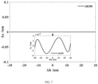
- the position error of each diffraction order may be obtained by simulation when the top tilt asymmetry changes in a range of [-30 nm, 30 nm], as shown in FIG. 7 . It may be seen that when the asymmetry changes, there are differences in the position errors of each diffraction order. The higher the diffraction order, the smaller the position error ⁇ x caused by the asymmetry; and the greater the asymmetry, the greater the position error of each diffraction order.
- the position error ⁇ x is a function of diffraction order m, and thus different m has different ⁇ x . Therefore, ⁇ x caused by the asymmetry may be reduced according to the difference.
- a weight vector ⁇ w m ⁇ of the diffraction order is orthogonal to a position error vector ⁇ x m ⁇ , and a sum of w m is guaranteed to be 1.
- the corrected position error is shown in FIG. 6 .
- the maximum position error is less than 4 ⁇ 10 -8 nm, which may be ignored.
Landscapes
- Physics & Mathematics (AREA)
- General Physics & Mathematics (AREA)
- Length Measuring Devices By Optical Means (AREA)
- Exposure Of Semiconductors, Excluding Electron Or Ion Beam Exposure (AREA)
Abstract
Description
- The present disclosure relates to the technical fields of semiconductors, integrated circuits, and precision measurement, and in particular to a method of reducing an impact of phase grating asymmetry on a position measurement accuracy.
- Phase grating position measurement technology has the characteristics of high measurement accuracy and less environmental impact, which is widely used in the fields of integrated circuits, precision processing, and precision measurement. This technology uses spatially coherent light to irradiate a phase grating to generate diffraction beams at all orders, and enables +m diffraction order and - m diffraction order to interfere, then scans the phase grating to generate a measurement signal with sine change, and finally obtains the position information of the grating by fitting the measurement signal. With the continuous development of application fields, especially the continuous shrinking of technological nodes in the field of integrated circuits, higher requirements are put forward for the measurement accuracy of a grating position sensor. However, a phase grating structure changes due to the impact of etching, deposition, chemical mechanical polishing, and a temperature change during the processing and subsequent processing of the phase grating. According to a principle of phase grating position measurement, an asymmetric change in the grating structure leads to a measurement error. Therefore, it is desired to analyze the impact of grating asymmetry on the measurement accuracy and reduce such impact.
- When analyzing the impact of grating asymmetry on the position measurement accuracy, a scanning electron microscope and the like are generally used to accurately measure a morphology of the grating, and then a diffraction field of the asymmetric grating is calculated by rigorously solving Maxwell's equations, such as Rigorous Coupled Wave Analysis (RCWA) or Finite Difference Time Domain (FDTD), so that the impact of asymmetry on the position measurement accuracy may be obtained, and the impact of asymmetry on the position measurement accuracy may be further reduced. However, different grating marks have different asymmetries, and the same grating mark may also result in different asymmetric changes due to factors such as clamping. Meanwhile, the scanning electron microscopy has a strict environmental requirement and a slow measurement speed, and is destructive. Although the method of rigorously solving Maxwell's equations has a high accuracy, it takes a long time. Therefore, the method requires a lot of time and is expensive.
- In view of the above, the main objective of the present disclosure is to provide a method of reducing an impact of phase grating asymmetry on a position measurement accuracy, so as to partially solve at least one of the above-mentioned technical problems.
- In order to achieve the above-mentioned objectives, as an aspect of the present disclosure, there is provided a method of reducing an impact of phase grating asymmetry on a position measurement accuracy, including:
- determining an asymmetry change range according to a phase grating design value and a processing accuracy, and then determining an asymmetric grating structure;
- establishing an asymmetric grating simulation model;
- inputting the asymmetric grating structure into the asymmetric grating simulation model, and simulating a position error curve of each diffraction order within the asymmetry change range; and
- determining a weight of each diffraction order according to an obtained difference in position error of each diffraction order, so as to reduce an impact of an asymmetric change.
- The establishing the asymmetric grating simulation model includes:
- deducing, according to a principle of phase grating position measurement, a calculation equation for the impact of asymmetry on the measurement accuracy;
- establishing, according to a scalar diffraction theory, an asymmetric grating model to obtain a diffraction field of an asymmetric grating, and then obtaining the impact of asymmetry on the position measurement accuracy according to the calculation equation.
- The method further includes a step for verification, and the step for verification includes verifying a corrected position error curve, so as to determine the weight is valid within the determined asymmetry change range.
- The principle of phase grating position measurement is: an incident beam with a wavelength λ is vertically incident on a phase grating to generate a diffraction beam at each order, +m diffraction order and -m diffraction order are interfered by an optical module; a periodic measurement signal is generated by scanning the phase grating; and position information of the phase grating is obtained from the measurement signal.
- The calculation equation for the impact of asymmetry on the measurement accuracy is:

- The obtaining the diffraction field of the asymmetric grating includes analyzing a diffraction field of a top tilted grating, and then deducing the diffraction field of the asymmetric grating.
- The diffraction field of the top tilted grating is expressed as:

- The asymmetric grating model includes a top, a bottom, a sidewall, and a vertex angle each having symmetry.
- A ridge of the asymmetric grating model is divided into four parts, G1, G2, G3, and G4 respectively, and the diffraction field of the asymmetric grating is expressed as:

- wherein


- wherein h1, h2, h3 and h4 represent heights of grating ridges in G1, G2, G3, and G4, respectively, x1, x2, x3, and x 4 represent center positions of G1, G2, G3, and G4, respectively, and f1, f2, f3, and f4 represent duty cycles of G1, G2, G3, and G4, respectively.
- A weight vector {wm } of the diffraction order is orthogonal to a position error vector {Δxm }, and a sum of wm is 1, so as to reduce an asymmetric position error.
- Based on the above-mentioned technical solution, it may be seen that the method of reducing an impact of phase grating asymmetry on the position measurement accuracy in the present disclosure has at least part of following beneficial effects with respect to the prior art.
- The method proposed by the present disclosure does not require measuring the morphology of the grating, but only needs to determine the asymmetry change range of the grating according to the processing accuracy, so as to reduce the impact of asymmetry change within the range on the position measurement accuracy.
- The method proposed by the present disclosure has strong process adaptability. Different asymmetries are caused by different process flows, and the asymmetries at different positions on the same silicon wafer are also inconsistent. However, the method may reduce the impact of asymmetry change within the range on the position measurement accuracy according to the change range.
- The method proposed by the present disclosure has low cost and strong real-time performance. Since the method does not require additional hardware to complete testing, the method avoids measuring asymmetry by means of scanning electron microscopy and process testing verification, thereby reducing costs. In addition, since the asymmetry change range may be determined in advance according to the process flow and the processing accuracy, thereby reducing the impact of asymmetry on the position measurement accuracy, the method has strong real-time performance.
- For a more complete understanding of the present disclosure and its advantages, reference is now made to the following description in combination with the accompanying drawings.
-
FIG. 1 shows a schematic flowchart of a method of reducing an impact of phase grating asymmetry on a position measurement accuracy of the present disclosure. -
FIG. 2 shows a schematic diagram of determining an asymmetric grating structure. -
FIG. 3 shows a schematic diagram of a top tilted grating structure within a period. -
FIG. 4 shows a schematic diagram of an asymmetric grating structure. -
FIG. 5 shows a schematic diagram of a decomposition of a mark structure. -
FIG. 6 shows a position error of each diffraction order when a top tilt asymmetry changes in a range of [-30 nm, 30 nm]. -
FIG. 7 shows a position error curve when a top tilt asymmetry changes in a range of [-30 nm, 30 nm] after assigning weights to measurement positions of different diffraction orders. - In order to make the objectives, technical solutions, and advantages of the present disclosure more apparent and understandable, the present disclosure is further described in detail in combination with specific embodiments and with reference to the accompanying drawings.
- The present disclosure proposes a method of reducing an impact of phase grating asymmetry on the position measurement accuracy. The method first determines an approximate morphology of a grating according to a design value of a phase grating and a range of grating processing. Then, according to the scalar diffraction theory, a grating analysis model is established to obtain the impact of asymmetric change on the measurement accuracy within the processing range. According to sensitivity differences of different diffraction orders to the asymmetric change, weights are assigned to measurement positions of different diffraction orders to reduce the impact of asymmetry on the position measurement accuracy. The method does not require measuring the morphology of the grating, but only needs to determine the asymmetry change range of the grating according to a processing accuracy, so as to reduce the impact of asymmetry change within the range on the position measurement accuracy.
- As shown in
FIG. 1 , a schematic flowchart of a method of reducing an impact of phase grating asymmetry on a position measurement accuracy includes following steps. - According to a phase grating design value and a processing accuracy, an asymmetry change range is determined, as shown in
FIG. 2 . For example, a grating design period d = 16 µm, a groove depth h = 200 nm, and a gating ridge width fd = 8 µm. According to the processing accuracy, assuming that the grating only has the asymmetry with a top tilt, a range of asymmetry of the top tilt is determined to be Δh ∈ [-30 nm, 30 nm]. - Firstly, according to a principle of phase grating position measurement, a calculation equation for an impact of asymmetry on the measurement accuracy is deduced. Then, according to a scalar diffraction theory, an asymmetric grating model is established to obtain a diffraction field of an asymmetric grating, and then the impact of asymmetry on the position measurement accuracy is obtained according to the calculation equation.
- A principle of a phase grating position sensor is: an incident beam with a wavelength λ is vertically incident on the phase grating to generate a diffraction beam at each order, and +m diffraction order and -m diffraction order are interfered by an optical module. A periodic measurement signal is generated by scanning the phase grating. Position information of the phase grating is obtained from the measurement signal.
- Assuming a position of the phase grating is x0, the incident beam is a parallel beam with a unit amplitude, and an initial phase is 0, then a complex amplitude of the +mth diffraction order is:

- Am is an amplitude of the +mth diffraction order, ϕ m is a phase after grating diffraction, d is a grating period, and x is a scanning motion position.
- A complex amplitude of the -mth diffraction order is:

- A-m is an amplitude of the -mth diffraction order, ϕ-m is a phase after grating diffraction. An interference light intensity is:

- A contrast ratio of the measurement signal is:

- Let Δϕm = ϕm - ϕ-m, then the position of the grating is:

- When the phase grating is a symmetric grating, Am = A-m and ϕ m = ϕ-m , then equation (5) is expressed as:

- At this point, the contrast ratio V of the measurement signal is 1, and the position x0 of the grating may be accurately obtained.
- When the phase grating is an asymmetric grating, Am ≠ A-m and ϕ m ≠ ϕ -m, then a resulting position error is:

- Therefore, when the phase grating is the asymmetric grating, not only the contrast ratio V of the measurement signal is reduced, but also the measurement position error is caused.
- In order to analyze the impact of asymmetry on the measurement accuracy, it is desired to obtain a form of a diffraction field of the asymmetric grating. According to the scalar diffraction theory, the method first analyzes a diffraction field of the top tilted grating, and then deduces the diffraction field of any asymmetric grating.
- A top tilted asymmetric grating structure is shown in
FIG. 3 . d is a grating period, l is a width of the gating ridge, f is a duty cycle and defined as l/d, h is a height of a grating ridge center, and Δh is an asymmetric height. It is assumed that the grating has infinite periods along the x-axis and extends infinitely perpendicular to the plane of the paper. - A coordinate system as shown in
FIG. 3 is established, and the grating structure is expressed as:

n is a positive integer. A reflection function of the grating may be expressed as:

- λ is an incident wavelength, and r is a reflection coefficient of a grating material. According to the scalar diffraction theory, when the incident beam is a plane wave with a unit amplitude, the diffraction field of the mth diffraction order may be expressed as:

- By substituting equation (9) into equation (10), it may be obtained that:

m ≠ 0. - It is assumed that each of the bottom, the sidewall, and the vertex angle of the asymmetric grating G is asymmetric, as shown in
FIG. 4 . The entire ridge are divided into four parts, G1, G2, G3, and G4 respectively, center positions of G1, G2, G3, and G4 are x1, x2, x3, and x 4 respectively, and the widths are f1d, f2d, f3d, and f4d, respectively. - According to the Fourier's theorem, a diffraction field


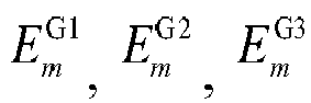

FIG. 5 .


- By substituting equation (11) and equation (13) into equation (12), the diffraction field

- According to the equation in
step 2, the position error of each diffraction order may be obtained by simulation when the top tilt asymmetry changes in a range of [-30 nm, 30 nm], as shown inFIG. 7 . It may be seen that when the asymmetry changes, there are differences in the position errors of each diffraction order. The higher the diffraction order, the smaller the position error Δx caused by the asymmetry; and the greater the asymmetry, the greater the position error of each diffraction order. - In order to improve the measurement accuracy, it is desired to control the position error caused by asymmetry. According to equation (7), the position error Δx is a function of diffraction order m, and thus different m has different Δx. Therefore, Δx caused by the asymmetry may be reduced according to the difference.
- Assuming that a position measurement sensor may collect measurement signals from the 1st diffraction order to the nth diffraction order, each diffraction order m results in a position error of Δxm , and an actual position of the grating is x 0, then the measurement result of the mth diffraction order is:

- Let a measurement result x of the grating position be:

- By substituting equation (14) into equation (15), it may be obtained that:

- Therefore, when there is no position error, i.e., x = x 0, it is required that:

- Therefore, in order to reduce an asymmetric position error, it is desired that a weight vector {wm} of the diffraction order is orthogonal to a position error vector {Δxm }, and a sum of wm is guaranteed to be 1. Based on the method, it may be determined that {wm } = {0, 0.0817, -0.8872, 0.5107, 1.2947}, where m = 1, 3, 5, 7, 9.
- Using the weight, the corrected position error is shown in
FIG. 6 . When the top tilt asymmetry changes within a range of [-30 nm, 30 nm], the maximum position error is less than 4 × 10⁻⁸ nm, which may be ignored. - The specific embodiments described above further explain objectives, technical solutions and beneficial effects of the present disclosure in detail. It should be understood that the specific embodiments described above are only specific embodiments of the present disclosure, and should not be used to limit the present disclosure. Any modifications, equivalent substitutions, improvements and the like made within the spirit and principle of the present disclosure should be included in the protection scope of the present disclosure.
Claims (10)
- A method of reducing an impact of phase grating asymmetry on a position measurement accuracy, comprising:determining an asymmetry change range according to a phase grating design value and a processing accuracy, and then determining an asymmetric grating structure;establishing an asymmetric grating simulation model;inputting the asymmetric grating structure into the asymmetric grating simulation model, and simulating a position error curve of each diffraction order within the asymmetry change range; anddetermining a weight of each diffraction order according to an obtained difference in position error of each diffraction order, so as to reduce an impact of an asymmetric change.
- The method according to claim 1, wherein the establishing the asymmetric grating simulation model comprises:deducing, according to a principle of phase grating position measurement, a calculation equation for the impact of asymmetry on the measurement accuracy;establishing, according to a scalar diffraction theory, an asymmetric grating model to obtain a diffraction field of an asymmetric grating, and then obtaining the impact of asymmetry on the position measurement accuracy according to the calculation equation.
- The method according to claim 1, further comprising a step for verification, wherein the step for verification comprises verifying a corrected position error curve, so as to determine the weight is valid within the determined asymmetry change range.
- The method according to claim 2, wherein the principle of phase grating position measurement is: an incident beam with a wavelength λ is vertically incident on a phase grating to generate a diffraction beam at each order, +m diffraction order and -m diffraction order are interfered by an optical module; a periodic measurement signal is generated by scanning the phase grating; and position information of the phase grating is obtained from the measurement signal.
- The method according to claim 2, wherein the calculation equation for the impact of asymmetry on the measurement accuracy is:

- The method according to claim 2, wherein the obtaining the diffraction field of the asymmetric grating comprises analyzing a diffraction field of a top tilted grating, and then deducing the diffraction field of the asymmetric grating.
- The method according to claim 6, wherein the diffraction field of the top tilted grating is expressed as:

- The method according to claim 2, wherein the asymmetric grating model comprises a top, a bottom, a sidewall, and a vertex angle each having symmetry.
- The method according to claim 8, wherein a ridge of the asymmetric grating model is divided into four parts, G1, G2, G3, and G4 respectively, and the diffraction field of the asymmetric grating is expressed as:
 wherein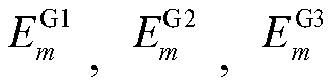

 wherein h 1, h2, h3 and h 4 represent heights of grating ridges in G1, G2, G3, and G4, respectively, x1, x2, x3, and x 4 represent center positions of G1, G2, G3, and G4, respectively, and f1, f2, f3 , and f4 represent duty cycles of G1, G2, G3, and G4, respectively.
 - The method according to claim 5, wherein a weight vector {wm } of the diffraction order is orthogonal to a position error vector {Δxm }, and a sum of wm is 1, so as to reduce an asymmetric position error.
Applications Claiming Priority (2)
| Application Number | Priority Date | Filing Date | Title |
|---|---|---|---|
| CN202110084779.XA CN112833790B (en) | 2021-01-21 | 2021-01-21 | A Method for Reducing the Influence of Phase Grating Asymmetry on Position Measurement Accuracy |
| PCT/CN2021/118791 WO2022156249A1 (en) | 2021-01-21 | 2021-09-16 | Method for reducing impact of phase grating asymmetry on position measurement precision |
Publications (2)
| Publication Number | Publication Date |
|---|---|
| EP4283249A1 true EP4283249A1 (en) | 2023-11-29 |
| EP4283249A4 EP4283249A4 (en) | 2025-07-02 |
Family
ID=75929344
Family Applications (1)
| Application Number | Title | Priority Date | Filing Date |
|---|---|---|---|
| EP21920627.3A Withdrawn EP4283249A4 (en) | 2021-01-21 | 2021-09-16 | Method for reducing the impact of phase grating asymmetry on position measurement precision |
Country Status (4)
| Country | Link |
|---|---|
| EP (1) | EP4283249A4 (en) |
| JP (1) | JP7623506B2 (en) |
| CN (1) | CN112833790B (en) |
| WO (1) | WO2022156249A1 (en) |
Families Citing this family (5)
| Publication number | Priority date | Publication date | Assignee | Title |
|---|---|---|---|---|
| CN112833790B (en) * | 2021-01-21 | 2023-03-14 | 中国科学院微电子研究所 | A Method for Reducing the Influence of Phase Grating Asymmetry on Position Measurement Accuracy |
| CN116222422B (en) * | 2023-01-17 | 2025-09-23 | 中国科学院微电子研究所 | Phase grating position measurement system and method for measuring structural parameters |
| CN116105599B (en) * | 2023-01-17 | 2025-10-24 | 中国科学院微电子研究所 | Error detection method and device for asymmetric grating marks |
| CN118818761B (en) * | 2024-09-05 | 2025-08-12 | 南京工业职业技术大学 | An optimization method for the simulation model of non-ideal volume holographic grating |
| CN121409092B (en) * | 2025-12-26 | 2026-03-27 | 歌尔光学科技有限公司 | Laser interferometer, measurement method thereof, optical detection system, and storage medium |
Family Cites Families (12)
| Publication number | Priority date | Publication date | Assignee | Title |
|---|---|---|---|---|
| JP3550605B2 (en) * | 1995-09-25 | 2004-08-04 | 株式会社ニコン | Position detection method, exposure method using the same, semiconductor device using the exposure method, method for manufacturing liquid crystal display element or thin-film magnetic head, position detection apparatus, and exposure apparatus having the same |
| US7515279B2 (en) * | 2001-03-02 | 2009-04-07 | Nanometrics Incorporated | Line profile asymmetry measurement |
| EP1431833A3 (en) * | 2002-12-16 | 2009-04-15 | ASML Netherlands B.V. | Lithographic apparatus, device manufacturing method, and device manufactured thereby |
| EP1678466A4 (en) * | 2003-09-12 | 2008-07-30 | Accent Optical Tech Inc | Line profile asymmetry measurement |
| WO2010145951A2 (en) * | 2009-06-17 | 2010-12-23 | Asml Netherlands B.V. | Method of overlay measurement, lithographic apparatus, inspection apparatus, processing apparatus and lithographic processing cell |
| WO2017032534A2 (en) | 2015-08-27 | 2017-03-02 | Asml Netherlands B.V. | Lithographic apparatus and device manufacturing method |
| DE102016210434A1 (en) * | 2016-06-13 | 2017-12-14 | Dr. Johannes Heidenhain Gmbh | Optical position measuring device |
| US11187995B2 (en) * | 2016-11-23 | 2021-11-30 | Asml Netherlands B.V. | Metrology using a plurality of metrology target measurement recipes |
| WO2019063245A1 (en) * | 2017-09-28 | 2019-04-04 | Asml Netherlands B.V. | Lithographic method |
| CN110967948B (en) * | 2019-11-29 | 2021-08-13 | 中国科学院微电子研究所 | Alignment Error Measurement Method |
| CN111610586B (en) * | 2020-06-24 | 2022-04-29 | 中国科学院微电子研究所 | Design method and system for a diffraction grating |
| CN112833790B (en) * | 2021-01-21 | 2023-03-14 | 中国科学院微电子研究所 | A Method for Reducing the Influence of Phase Grating Asymmetry on Position Measurement Accuracy |
-
2021
- 2021-01-21 CN CN202110084779.XA patent/CN112833790B/en active Active
- 2021-09-16 JP JP2023544410A patent/JP7623506B2/en active Active
- 2021-09-16 EP EP21920627.3A patent/EP4283249A4/en not_active Withdrawn
- 2021-09-16 WO PCT/CN2021/118791 patent/WO2022156249A1/en not_active Ceased
Also Published As
| Publication number | Publication date |
|---|---|
| WO2022156249A1 (en) | 2022-07-28 |
| JP7623506B2 (en) | 2025-01-28 |
| CN112833790A (en) | 2021-05-25 |
| EP4283249A4 (en) | 2025-07-02 |
| CN112833790B (en) | 2023-03-14 |
| JP2024503910A (en) | 2024-01-29 |
Similar Documents
| Publication | Publication Date | Title |
|---|---|---|
| CN112833790B (en) | A Method for Reducing the Influence of Phase Grating Asymmetry on Position Measurement Accuracy | |
| US10732516B2 (en) | Process robust overlay metrology based on optical scatterometry | |
| US5164790A (en) | Simple CD measurement of periodic structures on photomasks | |
| TWI596736B (en) | Like device scattering overlay | |
| US8472013B2 (en) | Refractive index distribution measurement method and apparatus that measure transmission wavefronts of a test object immersed in different media having refractive index lower than that of the test object | |
| US8142965B2 (en) | Method and system for measuring in patterned structures | |
| TW201830161A (en) | Design and correction using stack difference | |
| US12235097B2 (en) | Diffractive optical element for a test interferometer | |
| US8004679B2 (en) | Target design and methods for scatterometry overlay determination | |
| CN114264632B (en) | An in-situ calibration method for the polarization effect of the objective lens in an angle-resolved scatterometer | |
| CN107917665B (en) | Method and apparatus for determining the position of a light spot | |
| US9646804B2 (en) | Method for calibration of a CD-SEM characterisation technique | |
| CN101331378A (en) | Selecting identity cell configurations for repeating structures in optical metrology | |
| US7430052B2 (en) | Method for correlating the line width roughness of gratings and method for measurement | |
| CN107345788A (en) | A kind of directional light low-light spot optical critical dimension analytical equipment and detection method | |
| KR101059690B1 (en) | Refractive index measurement system and method for flat media using interference between transmitted and reflected light | |
| US7777880B2 (en) | Metrological characterisation of microelectronic circuits | |
| Silver et al. | Comparison of measured optical image profiles of silicon lines with two different theoretical models | |
| CN112987504A (en) | Focus calibration system and focus calibration method based on light beam scanning angle modulation | |
| US12541154B2 (en) | Optical method and apparatus for quickly realizing precise calibration of lithography system | |
| JPH07134013A (en) | Surface shape measuring method and projection exposure apparatus | |
| Scholze et al. | Use of EUV scatterometry for the characterization of line profiles and line roughness on photomasks | |
| US6057914A (en) | Method for detecting and identifying a lens aberration by measurement of sidewall angles by atomic force microscopy | |
| CN110967948A (en) | Alignment Error Measurement Method | |
| Murnane et al. | Developed photoresist metrology using scatterometry |
Legal Events
| Date | Code | Title | Description |
|---|---|---|---|
| STAA | Information on the status of an ep patent application or granted ep patent |
Free format text: STATUS: THE INTERNATIONAL PUBLICATION HAS BEEN MADE |
|
| PUAI | Public reference made under article 153(3) epc to a published international application that has entered the european phase |
Free format text: ORIGINAL CODE: 0009012 |
|
| STAA | Information on the status of an ep patent application or granted ep patent |
Free format text: STATUS: REQUEST FOR EXAMINATION WAS MADE |
|
| 17P | Request for examination filed |
Effective date: 20230821 |
|
| AK | Designated contracting states |
Kind code of ref document: A1 Designated state(s): AL AT BE BG CH CY CZ DE DK EE ES FI FR GB GR HR HU IE IS IT LI LT LU LV MC MK MT NL NO PL PT RO RS SE SI SK SM TR |
|
| DAV | Request for validation of the european patent (deleted) | ||
| DAX | Request for extension of the european patent (deleted) | ||
| A4 | Supplementary search report drawn up and despatched |
Effective date: 20250602 |
|
| RIC1 | Information provided on ipc code assigned before grant |
Ipc: G03F 7/00 20060101ALI20250526BHEP Ipc: G03F 9/00 20060101ALI20250526BHEP Ipc: G01B 11/00 20060101AFI20250526BHEP |
|
| STAA | Information on the status of an ep patent application or granted ep patent |
Free format text: STATUS: THE APPLICATION HAS BEEN WITHDRAWN |
|
| 18W | Application withdrawn |
Effective date: 20250916 |