EP4282094B1 - Kohärenter empfänger mit niedrigen durch voa induzierten phasenänderungen - Google Patents
Kohärenter empfänger mit niedrigen durch voa induzierten phasenänderungen Download PDFInfo
- Publication number
- EP4282094B1 EP4282094B1 EP23715651.8A EP23715651A EP4282094B1 EP 4282094 B1 EP4282094 B1 EP 4282094B1 EP 23715651 A EP23715651 A EP 23715651A EP 4282094 B1 EP4282094 B1 EP 4282094B1
- Authority
- EP
- European Patent Office
- Prior art keywords
- voa
- signal
- path
- phase change
- coherent receiver
- Prior art date
- Legal status (The legal status is an assumption and is not a legal conclusion. Google has not performed a legal analysis and makes no representation as to the accuracy of the status listed.)
- Active
Links
Images






Classifications
-
- H—ELECTRICITY
- H04—ELECTRIC COMMUNICATION TECHNIQUE
- H04B—TRANSMISSION
- H04B10/00—Transmission systems employing electromagnetic waves other than radio-waves, e.g. infrared, visible or ultraviolet light, or employing corpuscular radiation, e.g. quantum communication
- H04B10/60—Receivers
- H04B10/61—Coherent receivers
Definitions
- a short p-i-n junction VOA providing attenuation of light through carrier injection, i.e., a CI-VOA, will change the phase of an incoming signal (i.e., introduce chirp) in addition to providing attenuation.
- Another existing approach includes using a Mach Zehnder interferometer (MZI) with a phase changing element in each arm (i.e., one each for the X and Y channels). By changing the relative phase difference between the arms of the MZI, one can produce a variable attenuator.
- MZI Mach Zehnder interferometer
- a CI-VOA, placed in each arm can produce just enough phase shift (at least ⁇ ) without causing too much intrinsic absorption.
- a coherent receiver includes a receive signal, SIG, path including i) an input configured to connect a receive signal, ii) one or more signal paths connected to the input and to one or more optical hybrids, and iii) at least one first variable optical attenuator, VOA; and a local oscillator, LO, signal path including an input configured to connect to an LO and the one or more optical hybrids;
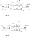
- the optical receiver includes a VOA-induced phase change compensation mechanism that reduces any VOA-induced phase change in a SIG-LO beat signal due to the at least one first VOA being in the signal path, wherein the VOA-induced phase change compensation mechanism includes one or more of at least one second VOA in the LO path before the one or more optical hybrids, the at least one second VOA configured to add a LO phase change to the LO path to at least partially compensate for the VOA-induced phase change in the signal path due to the at least one first VOA, and a chirp-free Mach-Zehnder
- the at least one VOA (first VOA) and the at least one tandem VOA (second VOA) can each be a same type of VOA.
- the at least one VOA and the at least one tandem VOA can each be a different type of VOA.
- the at least one VOA and the at least one tandem VOA can each be any of a current injection VOA (CI-VOA) and a chirped Mach-Zehnder (MZ) interferometer (MZI) VOA (MZI-VOA).
- CI-VOA current injection VOA
- MZI Mach-Z interferometer
- the at least one VOA and the at least one tandem VOA can each be controlled with a same control signal.
- the at least one VOA and the at least one tandem VOA can each be controlled with independent control signals.
- the at least one VOA and the at least one tandem VOA cam each include different phase versus attenuation characteristics, which are configured appropriately.
- the at least one VOA and the at least one tandem VOA can each have their attenuation set based to provide a same amplitude of a corresponding beat signal.
- the one or more signal paths can include two signal paths, one for an X-polarization and one for a Y-polarization, wherein the VOA in each of the one or more signal paths include a VOA(X) and a VOA(Y).
- the VOA-induced phase change compensation mechanism can include at least one tandem VOA in the LO path.
- the at least one tandem VOA can include two VOAs including a LO VOA(X) and a LO VOA(Y) in the LO signal path.
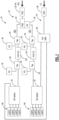
- FIG. 1 is a block diagram of a coherent optical receiver 10 with internal VOAs 12X, 12Y on the X and Y receive signal path.
- the coherent optical receiver 10 can be referred to as an ultra-high bandwidth (UHB) ICR.
- the coherent optical receiver 10 includes a receive signal (SIG) path 14 and a LO signal path 16.
- the receive signal path 14 includes an X-polarization signal path 18X and a Y-polarization signal path 18Y.
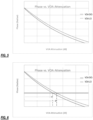
- FIGS. 2A - 2D are graphs of characteristics of a typical VOA using a p-i-n junction in carrier injection mode (forward voltage operation). These can be referred to herein as current-injection VOAs (CI-VOA).
- the VOAs provide attenuation of light through carrier injection when the junction is forward biased.
- the intrinsic region is located at the center of the waveguide where light is travelling.
- the presence of injected carriers in the waveguide also has the consequence of changing the refractive index (as implied from Soref's equations, see Soref et al., "Electrooptical effects in silicon.” IEEE J. Quantum Electron., 23.1 (1987): 123-129 , referred to herein as Soref et al.).
- a significant phase change close to 10 rads would be obtained for an attenuation of 20 dB.
- R is the photodiode responsivity
- P s is the optical power from the SIG port entering the balanced pair of HSPD (high-speed photodiodes)
- P LO is the optical power from the Local Oscillator (LO) port
- ⁇ s and ⁇ LO are respectively the optical (angular) frequency of the incoming signal
- LO Local Oscillator
- ⁇ s and ⁇ LO are the phase of these optical signals. Note that these phases include the phase noise on both SIG and LO lasers, the phase modulation on the received signal from the SIG port, and the VOA-induced phase change.
- VOA 42 in the LO signal path 16 is somewhat restricting the attenuation on the X and Y channels to be the same. If one wants to keep adjusting the X and Y channel's attenuation independently, one can use two VOAs 42X, 42Y in the LO path, after the X-Y splitter (1 ⁇ 2 MMI 38) in the LO signal path 16, as illustrated in FIG. 4 .
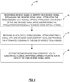
- FIG. 8 is a flowchart of a process 80 for VOA-induced phase change cancelation.
- the process 80 can be implemented in the coherent receiver 10 or the like.
- the process 80 includes receiving a receive signal at an input of a receive signal path having one or more signal paths, attenuating the receive signal via a variable optical attenuator (VOA) in each the one or more signal paths, and providing the attenuated receive signals to one or more optical hybrids (step 82); receiving a local oscillator (LO) signal, attenuating the LO signal with one or more complementary VOAs, and providing the attenuated LO signal to the one or more optical hybrids (step 84); and setting the one or more complementary VOAs to substantially cancel any phase changes from the VOA in each of the one or more signal paths (step 86).
- VOA variable optical attenuator
- a coherent receiver includes a receive signal path including i) an input configured to connect a receive signal, ii) one or more signal paths connected to the input and to one or more optical hybrids, and iii) a variable optical attenuator (VOA) in each of the one or more signal paths; and a local oscillator (LO) signal path including i) an input configured to connect to an LO and the one or more optical hybrids, and ii) one or more complementary VOAs located between the input and the one or more optical hybrids, wherein the one or more complementary VOAs are configured to substantially cancel any phase changes from the VOA in each of the one or more signal paths.
- LO local oscillator
- the VOA in each of the one or more signal paths and the one or more complementary VOAs can each be controlled with a same control signal.
- the VOA in each of the one or more signal paths and the one or more complementary VOAs can each be controlled with independent control signals.
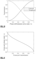
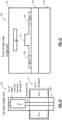
- FIG. 18 shows diagrams of an embodiment of a single arm 204, 206 of the MZI VOA 200 with combined p-i-n and resistive heater (electrical connections).
- the side doped sections (p++ and n++) forming the p-i-n junctions are re-used as resistive heaters.
- the resistive part can extend past the p-i-n section.
- the junction and heater controls are now interlinked, adding complexity to the control loops, but simplifying the silicon photonics implementation.
- the resistor values are to be carefully engineered by playing with dopant levels (e.g., using a plurality) and form factors (affecting sheet resistance values). The resistor values need not be all identical.
- the VOAs 12, 42 in the coherent optical receiver 10 can utilize the MZI VOA 200.
- the coherent optical receiver 10 includes the VOA 42 that when actuated generates a very low [SIG ⁇ LO] phase perturbation.
- the VOA-induced phase change compensation mechanism includes at least one tandem VOA in the LO path.
- the at least one VOA and the at least one tandem VOA can each be a same type of VOA or each be a different type of VOA.
- the at least one VOA and the at least one tandem VOA can each be any of a current injection VOA (CI-VOA) and a chirped Mach-Zehnder (MZ) interferometer (MZI) VOA (MZI-VOA).
- CI-VOA current injection VOA
- MZI Mach-Z interferometer
- the at least one VOA and the at least one tandem VOA can each be controlled with a same control signal.
- the at least one VOA and the at least one tandem VOA can also each be controlled with independent control signals.
- FIG. 20 is a flowchart of a process 300 for a coherent receiver having low variable optical attenuator (VOA)-induced phase changes.
- the process 300 includes receiving a receive signal at an input of a receive signal path having one or more signal paths, attenuating the receive signal via at least one variable optical attenuator (VOA), and providing the attenuated receive signals to one or more optical hybrids (step 302); receiving a local oscillator (LO) signal, and providing the attenuated LO signal to the one or more optical hybrids (step 304); and compensating any VOA-induced phase change in a SIG-LO beat signal due to the at least one VOA (step 306).
- VOA variable optical attenuator
- the compensating can include (1) tandem VOAs for attenuating the LO signal such that the LO signal experiences similar VOA-induced phase change as the attenuated receive signals, or (2) utilizing a chirp-free Mach-Zehnder (MZ) interferometer for the attenuating.
- tandem VOAs for attenuating the LO signal such that the LO signal experiences similar VOA-induced phase change as the attenuated receive signals
- MZ Mach-Zehnder
- VOA induced phase change can be provides in units of rad RMS sec or rad Peak sec , and these can be related, e.g., rad Peak sec can be 2 - 4 times larger than rad RMS sec .
- RMS root mean square
- RAD radians
- FIG. 1 i.e., VOA only on the SIG path and not the LO path, can have a VOA induced phase change on the order of hundreds of thousands of these values, and this can be beyond the ability of a coherent DSP to track.
- the chirp Mach-Zehnder (MZ) interferometer on the SIG path described herein can have a VOA induced phase change on the order of tens of thousands of these values, a significant improvement from the Cl-VOA only on the SIG path, and typically well within the ability of a coherent DSP to track.
- the tandem VOA approach i.e., VOA on both the SIG path and the LO path, and the chirp-free MZ on the SIG path approach can have a VOA induced phase change on the order of thousands of these values.
- processors such as microprocessors; Central Processing Units (CPUs); Digital Signal Processors (DSPs): customized processors such as Network Processors (NPs) or Network Processing Units (NPUs), Graphics Processing Units (GPUs), or the like; Field-Programmable Gate Arrays (FPGAs); and the like along with unique stored program instructions (including both software and firmware) for control thereof to implement, in conjunction with certain non-processor circuits, some, most, or all of the functions of the methods and/or systems described herein.
- processors such as microprocessors; Central Processing Units (CPUs); Digital Signal Processors (DSPs): customized processors such as Network Processors (NPs) or Network Processing Units (NPUs), Graphics Processing Units (GPUs), or the like; Field-Programmable Gate Arrays (FPGAs); and the like along with unique stored program instructions (including both software and firmware) for control thereof to implement, in conjunction with certain non-processor circuits, some, most, or all
- circuitry configured to
- logic configured to
- some embodiments may include a non-transitory computer-readable medium having instructions stored thereon for programming a computer, server, appliance, device, at least one processor, circuit/circuitry, etc. to perform functions as described and claimed herein.
- Examples of such non-transitory computer-readable medium include, but are not limited to, a hard disk, an optical storage device, a magnetic storage device, a Read-Only Memory (ROM), a Programmable ROM (PROM), an Erasable PROM (EPROM), an Electrically EPROM (EEPROM), Flash memory, and the like.
- software can include instructions executable by one or more processors (e.g., any type of programmable circuitry or logic) that, in response to such execution, cause the one or more processors to perform a set of operations, steps, methods, processes, algorithms, functions, techniques, etc. as described herein for the various embodiments.
- processors e.g., any type of programmable circuitry or logic
Landscapes
- Physics & Mathematics (AREA)
- Electromagnetism (AREA)
- Engineering & Computer Science (AREA)
- Computer Networks & Wireless Communication (AREA)
- Signal Processing (AREA)
- Optical Communication System (AREA)
- Optical Modulation, Optical Deflection, Nonlinear Optics, Optical Demodulation, Optical Logic Elements (AREA)
Claims (13)
- Kohärenter Empfänger (10), umfassend:einen Empfangssignal-, SIG-, Pfad (14), der i) einen Eingang, der so konfiguriert ist, dass er ein optisches Empfangssignal verbindet, ii) einen oder mehrere Signalpfade, die mit dem Eingang und mit einem oder mehreren optischen Hybriden (32) verbunden sind, und iii) mindestens einen ersten variablen optischen Dämpfer, VOA, (12) beinhaltet; undeinen lokalen Oszillator-, LO-, Signalpfad (16), der einen Eingang beinhaltet, der so konfiguriert ist, dass er mit einem LO und dem einen oder den mehreren optischen Hybriden (32) verbunden werden kann;wobei der kohärente Empfänger (10) einen Kompensationsmechanismus für VOA-induzierte Phasenänderungen beinhaltet, der so konfiguriert ist, dass er jede VOA-induzierte Phasenänderung in einem SIG-LO-Schwebungssignal, die durch den mindestens einen ersten VOA (12), der sich im Signalpfad (14) befindet, bedingt ist, reduziert, wobei der Kompensationsmechanismus für VOA-induzierte Phasenänderungen eines oder mehrere von (1) mindestens einem zweiten VOA (42) im LO-Pfad (16) vor dem einen oder den mehreren optischen Hybriden (32), wobei der mindestens eine zweite VOA (42) so konfiguriert ist, dass er eine LO-Phasenänderung zum LO-Pfad (16) hinzufügt, um die VOA-induzierte Phasenänderung im Signalpfad (14), die durch den mindestens einen ersten VOA (12) bedingt ist, mindestens teilweise zu kompensieren, und (2) ein chirpfreies Mach-Zehnder-, MZ-, Interferometer beinhaltet, welches den mindestens einen ersten VOA (12) im Signalpfad (14) bildet.
- Kohärenter Empfänger (10) nach Anspruch 1, wobei der Kompensationsmechanismus für VOA-induzierte Phasenänderungen den mindestens einen zweiten VOA (42) im LO-Pfad (16) vor dem einen oder den mehreren optischen Hybriden (32) beinhaltet.
- Kohärenter Empfänger (10) nach Anspruch 2, wobei der mindestens eine erste VOA (12) und der mindestens eine zweite VOA (42) jeweils derselbe VOA-Typ sind.
- Kohärenter Empfänger (10) nach Anspruch 2, wobei der mindestens eine erste VOA (12) und der mindestens eine zweite VOA (42) jeweils ein unterschiedlicher VOA-Typ sind.
- Kohärenter Empfänger (10) nach einem der Ansprüche 2 bis 4, wobei der mindestens eine erste VOA (12) und der mindestens eine zweite VOA (42) jeweils einer von einem Strominjektions-VOA, CI-VOA, und einem gechirpten Mach-Zehnder-, MZ, Interferometer-, MZI, VOA, MZI-VOA, sind.
- Kohärenter Empfänger (10) nach einem der Ansprüche 2 bis 5, wobei der mindestens eine erste VOA (12) und der mindestens eine zweite VOA (42) jeweils so konfiguriert sind, dass sie mit einem von demselben Steuersignal und unabhängigen Steuersignalen gesteuert werden können.
- Kohärenter Empfänger (10) nach einem der Ansprüche 2 bis 6, wobei der mindestens eine erste VOA (12) und der mindestens eine zweite VOA (42) jeweils unterschiedliche Phasen-/Dämpfungseigenschaften beinhalten, die entsprechend konfiguriert sind.
- Kohärenter Empfänger (10) nach einem der Ansprüche 2 bis 7, wobei die Dämpfung des mindestens einen ersten VOA (12) und des mindestens einen zweiten VOA (42) jeweils darauf basierend eingestellt wird, dass sie dieselbe Amplitude eines entsprechenden Schwebungssignals bereitstellen.
- Kohärenter Empfänger (10) nach einem der Ansprüche 2 bis 8, wobei der eine oder die mehreren Signalpfade (14, 16) zwei Signalpfade, einen für eine X-Polarisation und einen für eine Y-Polarisation, beinhalten,
wobei der VOA in jedem des einen oder der mehreren Signalpfade einen VOA(X) und einen VOA(Y) beinhaltet. - Kohärenter Empfänger (10) nach Anspruch 9, wobei der mindestens eine zweite VOA (42) zwei VOAs beinhaltet, die einen LO VOA(X) und einen LO VOA(Y) im LO-Signalpfad (14) beinhalten.
- Kohärenter Empfänger (10) nach Anspruch 1, wobei das chirpfreie Mach-Zehnder- (MZ-) Interferometer beinhalteteinen p-i-n-Übergangsphasenschieber (212) zur schnellen Phasensteuerung, undeinen thermischen Phasenschieber, TPS, (202) zur langsamen Phasensteuerung.
- Kohärenter Empfänger (10) nach einem der Ansprüche 1 bis 10, wobei der Kompensationsmechanismus für VOA-induzierte Phasenänderungen so konfiguriert ist, dass er die VOA-induzierte Phasenänderung auf innerhalb von Tausenden oder weniger von


- Verfahren (300), das folgende Schritte umfasst:Empfangen (302) eines Empfangssignals an einem Eingang eines Empfangssignalpfads (14), der einen oder mehrere Signalpfade aufweist, Dämpfen des Empfangssignals über mindestens einen ersten variablen optischen Dämpfer (VOA) (12), und Bereitstellen der gedämpften Empfangssignale für einen oder mehrere optische Hybride;Empfangen (304) eines lokalen Oszillator-, LO-, Signals und Bereitstellen des gedämpften LO-Signals für den einen oder die mehreren optischen Hybride über einen LO-Pfad (14); undKompensieren (306) jeder VOA-induzierten Phasenänderung in einem SIG-LO-Schwebungssignal, die durch den mindestens einen ersten VOA (12), der sich im Signalpfad (14) befindet, bedingt ist, über einen oder mehrere (1) mindestens eines zweiten VOA (42) im LO-Pfad (14) vor einem oder mehreren optischen Hybriden (32), wobei der mindestens eine zweite VOA so konfiguriert ist, dass er eine LO-Phasenänderung zum LO-Pfad hinzufügt, um die VOA-induzierte Phasenänderung im Signalpfad, die durch den mindestens einen ersten VOA bedingt ist, mindestens teilweise zu kompensieren, und (2) eines chirpfreien Mach-Zehnder-, MZ-, Interferometers, welches den mindestens einen ersten VOA (12) im Signalpfad (14) bildet.
Applications Claiming Priority (2)
| Application Number | Priority Date | Filing Date | Title |
|---|---|---|---|
| US17/696,948 US12149291B2 (en) | 2022-03-17 | 2022-03-17 | Coherent receiver having low VOA-induced phase changes |
| PCT/US2023/015142 WO2023177640A1 (en) | 2022-03-17 | 2023-03-13 | Coherent receiver having low voa-induced phase changes |
Publications (2)
| Publication Number | Publication Date |
|---|---|
| EP4282094A1 EP4282094A1 (de) | 2023-11-29 |
| EP4282094B1 true EP4282094B1 (de) | 2024-07-10 |
Family
ID=87975507
Family Applications (1)
| Application Number | Title | Priority Date | Filing Date |
|---|---|---|---|
| EP23715651.8A Active EP4282094B1 (de) | 2022-03-17 | 2023-03-13 | Kohärenter empfänger mit niedrigen durch voa induzierten phasenänderungen |
Country Status (2)
| Country | Link |
|---|---|
| EP (1) | EP4282094B1 (de) |
| CN (1) | CN119156787B (de) |
Citations (1)
| Publication number | Priority date | Publication date | Assignee | Title |
|---|---|---|---|---|
| US20040008965A1 (en) * | 2002-07-09 | 2004-01-15 | Nortel Networks Limited | Current tuned Mach-Zehnder optical attenuator |
Family Cites Families (6)
| Publication number | Priority date | Publication date | Assignee | Title |
|---|---|---|---|---|
| JP5326584B2 (ja) * | 2009-01-09 | 2013-10-30 | 富士通株式会社 | 遅延処理装置,信号増幅装置,光電変換装置,アナログ/デジタル変換装置,受信装置および受信方法 |
| US8406621B2 (en) * | 2009-10-29 | 2013-03-26 | Teraxion Inc. | Method and apparatus for measuring a factor characterizing a balanced detection device |
| CN104487891B (zh) * | 2012-07-30 | 2018-09-28 | 富士通光器件株式会社 | 光接收回路 |
| CN203327014U (zh) * | 2013-03-15 | 2013-12-04 | 昂纳信息技术(深圳)有限公司 | 一种集成可调光衰减器的集成相关接收器 |
| CN107430312A (zh) * | 2015-03-09 | 2017-12-01 | 住友电工光电子器件创新株式会社 | 相干接收器 |
| CN111490827B (zh) * | 2019-04-08 | 2021-10-12 | Nano科技(北京)有限公司 | 单体集成相干收发器 |
-
2023
- 2023-03-13 EP EP23715651.8A patent/EP4282094B1/de active Active
- 2023-03-13 CN CN202380041294.XA patent/CN119156787B/zh active Active
Patent Citations (1)
| Publication number | Priority date | Publication date | Assignee | Title |
|---|---|---|---|---|
| US20040008965A1 (en) * | 2002-07-09 | 2004-01-15 | Nortel Networks Limited | Current tuned Mach-Zehnder optical attenuator |
Non-Patent Citations (1)
| Title |
|---|
| GAUDEN D ET AL: "Variable optical attenuator based on thermally tuned Mach-Zehnder interferometer within a twin core fiber", OPTICS COMMUNICATIONS, ELSEVIER, AMSTERDAM, NL, vol. 231, no. 1-6, 15 February 2004 (2004-02-15), pages 213 - 216, XP027338580, ISSN: 0030-4018, [retrieved on 20040123] * |
Also Published As
| Publication number | Publication date |
|---|---|
| EP4282094A1 (de) | 2023-11-29 |
| CN119156787B (zh) | 2025-06-13 |
| CA3210052A1 (en) | 2023-09-17 |
| CN119156787A (zh) | 2024-12-17 |
Similar Documents
| Publication | Publication Date | Title |
|---|---|---|
| Zhu et al. | Silicon integrated microwave photonic beamformer | |
| Xie et al. | Seven-bit reconfigurable optical true time delay line based on silicon integration | |
| Jeong et al. | Novel Optical 90 ^∘ Hybrid Consisting of a Paired Interference Based 2 \,*\, 4 MMI Coupler, a Phase Shifter and a 2 \,*\, 2 MMI Coupler | |
| Rasras et al. | Demonstration of a tunable microwave-photonic notch filter using low-loss silicon ring resonators | |
| US6751002B2 (en) | Method and apparatus for semiconductor-based integrated polarization modulator/compensator | |
| Joergensen et al. | Wavelength conversion by optimized monolithic integrated Mach-Zehnder interferometer | |
| Zanetto et al. | Dithering‐based real‐time control of cascaded silicon photonic devices by means of non‐invasive detectors | |
| Suzuki et al. | Slow-light-based variable symbol-rate silicon photonics DQPSK receiver | |
| US20170090268A1 (en) | Chirp suppressed ring resonator | |
| US10901153B2 (en) | Null bias mach-zehnder interferometer with ring resonators | |
| US20200145739A1 (en) | Low-crosstalk electro-optical mach-zehnder switch | |
| Chang et al. | Differential microring modulators for intensity and phase modulation: theory and experiments | |
| EP3650925B1 (de) | Optischer schalter mit mach-zehnder interferometer | |
| WO2016149289A1 (en) | Differential ring modulator | |
| Urick et al. | Microwave phase shifting using coherent photonic integrated circuits | |
| US20090074426A1 (en) | Monolithic dqpsk receiver | |
| Morton et al. | All-optical linearized Mach-Zehnder modulator | |
| Guo et al. | Integrated Self-Coherent Optical Transceivers for Data Center Applications Based on Thin-Film Lithium Niobate Platform | |
| Melikyan et al. | Inter-polarization mixers for coherent detection of optical signals | |
| US12149291B2 (en) | Coherent receiver having low VOA-induced phase changes | |
| CA3210052C (en) | Coherent receiver having low voa-induced phase changes | |
| CA2308638A1 (en) | Optical wavelength converter | |
| EP4282094A1 (de) | Kohärenter empfänger mit niedrigen durch voa induzierten änderungen | |
| Kurata et al. | Heterogeneously integrated PLC with low-loss spot-size converter and newly developed waveplate PBS for DC-DP-16QAM receiver | |
| Kang et al. | A hybrid electroabsorption modulator device for generation of high spectral-efficiency optical modulation formats |
Legal Events
| Date | Code | Title | Description |
|---|---|---|---|
| STAA | Information on the status of an ep patent application or granted ep patent |
Free format text: STATUS: UNKNOWN |
|
| STAA | Information on the status of an ep patent application or granted ep patent |
Free format text: STATUS: THE INTERNATIONAL PUBLICATION HAS BEEN MADE |
|
| PUAI | Public reference made under article 153(3) epc to a published international application that has entered the european phase |
Free format text: ORIGINAL CODE: 0009012 |
|
| STAA | Information on the status of an ep patent application or granted ep patent |
Free format text: STATUS: REQUEST FOR EXAMINATION WAS MADE |
|
| STAA | Information on the status of an ep patent application or granted ep patent |
Free format text: STATUS: EXAMINATION IS IN PROGRESS |
|
| 17P | Request for examination filed |
Effective date: 20230822 |
|
| AK | Designated contracting states |
Kind code of ref document: A1 Designated state(s): AL AT BE BG CH CY CZ DE DK EE ES FI FR GB GR HR HU IE IS IT LI LT LU LV MC ME MK MT NL NO PL PT RO RS SE SI SK SM TR |
|
| 17Q | First examination report despatched |
Effective date: 20231123 |
|
| P01 | Opt-out of the competence of the unified patent court (upc) registered |
Effective date: 20240108 |
|
| GRAP | Despatch of communication of intention to grant a patent |
Free format text: ORIGINAL CODE: EPIDOSNIGR1 |
|
| STAA | Information on the status of an ep patent application or granted ep patent |
Free format text: STATUS: GRANT OF PATENT IS INTENDED |
|
| DAV | Request for validation of the european patent (deleted) | ||
| DAX | Request for extension of the european patent (deleted) | ||
| INTG | Intention to grant announced |
Effective date: 20240429 |
|
| GRAS | Grant fee paid |
Free format text: ORIGINAL CODE: EPIDOSNIGR3 |
|
| GRAA | (expected) grant |
Free format text: ORIGINAL CODE: 0009210 |
|
| STAA | Information on the status of an ep patent application or granted ep patent |
Free format text: STATUS: THE PATENT HAS BEEN GRANTED |
|
| AK | Designated contracting states |
Kind code of ref document: B1 Designated state(s): AL AT BE BG CH CY CZ DE DK EE ES FI FR GB GR HR HU IE IS IT LI LT LU LV MC ME MK MT NL NO PL PT RO RS SE SI SK SM TR |
|
| REG | Reference to a national code |
Ref country code: CH Ref legal event code: EP |
|
| REG | Reference to a national code |
Ref country code: DE Ref legal event code: R096 Ref document number: 602023000228 Country of ref document: DE |
|
| REG | Reference to a national code |
Ref country code: NL Ref legal event code: FP |
|
| REG | Reference to a national code |
Ref country code: LT Ref legal event code: MG9D |
|
| PG25 | Lapsed in a contracting state [announced via postgrant information from national office to epo] |
Ref country code: PT Free format text: LAPSE BECAUSE OF FAILURE TO SUBMIT A TRANSLATION OF THE DESCRIPTION OR TO PAY THE FEE WITHIN THE PRESCRIBED TIME-LIMIT Effective date: 20241111 |
|
| REG | Reference to a national code |
Ref country code: AT Ref legal event code: MK05 Ref document number: 1702961 Country of ref document: AT Kind code of ref document: T Effective date: 20240710 |
|
| PG25 | Lapsed in a contracting state [announced via postgrant information from national office to epo] |
Ref country code: PT Free format text: LAPSE BECAUSE OF FAILURE TO SUBMIT A TRANSLATION OF THE DESCRIPTION OR TO PAY THE FEE WITHIN THE PRESCRIBED TIME-LIMIT Effective date: 20241111 |
|
| PG25 | Lapsed in a contracting state [announced via postgrant information from national office to epo] |
Ref country code: NO Free format text: LAPSE BECAUSE OF FAILURE TO SUBMIT A TRANSLATION OF THE DESCRIPTION OR TO PAY THE FEE WITHIN THE PRESCRIBED TIME-LIMIT Effective date: 20241010 |
|
| PG25 | Lapsed in a contracting state [announced via postgrant information from national office to epo] |
Ref country code: GR Free format text: LAPSE BECAUSE OF FAILURE TO SUBMIT A TRANSLATION OF THE DESCRIPTION OR TO PAY THE FEE WITHIN THE PRESCRIBED TIME-LIMIT Effective date: 20241011 Ref country code: FI Free format text: LAPSE BECAUSE OF FAILURE TO SUBMIT A TRANSLATION OF THE DESCRIPTION OR TO PAY THE FEE WITHIN THE PRESCRIBED TIME-LIMIT Effective date: 20240710 Ref country code: PL Free format text: LAPSE BECAUSE OF FAILURE TO SUBMIT A TRANSLATION OF THE DESCRIPTION OR TO PAY THE FEE WITHIN THE PRESCRIBED TIME-LIMIT Effective date: 20240710 |
|
| PG25 | Lapsed in a contracting state [announced via postgrant information from national office to epo] |
Ref country code: BG Free format text: LAPSE BECAUSE OF FAILURE TO SUBMIT A TRANSLATION OF THE DESCRIPTION OR TO PAY THE FEE WITHIN THE PRESCRIBED TIME-LIMIT Effective date: 20240710 |
|
| PG25 | Lapsed in a contracting state [announced via postgrant information from national office to epo] |
Ref country code: LV Free format text: LAPSE BECAUSE OF FAILURE TO SUBMIT A TRANSLATION OF THE DESCRIPTION OR TO PAY THE FEE WITHIN THE PRESCRIBED TIME-LIMIT Effective date: 20240710 |
|
| PG25 | Lapsed in a contracting state [announced via postgrant information from national office to epo] |
Ref country code: IS Free format text: LAPSE BECAUSE OF FAILURE TO SUBMIT A TRANSLATION OF THE DESCRIPTION OR TO PAY THE FEE WITHIN THE PRESCRIBED TIME-LIMIT Effective date: 20241110 Ref country code: AT Free format text: LAPSE BECAUSE OF FAILURE TO SUBMIT A TRANSLATION OF THE DESCRIPTION OR TO PAY THE FEE WITHIN THE PRESCRIBED TIME-LIMIT Effective date: 20240710 |
|
| PG25 | Lapsed in a contracting state [announced via postgrant information from national office to epo] |
Ref country code: HR Free format text: LAPSE BECAUSE OF FAILURE TO SUBMIT A TRANSLATION OF THE DESCRIPTION OR TO PAY THE FEE WITHIN THE PRESCRIBED TIME-LIMIT Effective date: 20240710 |
|
| PG25 | Lapsed in a contracting state [announced via postgrant information from national office to epo] |
Ref country code: RS Free format text: LAPSE BECAUSE OF FAILURE TO SUBMIT A TRANSLATION OF THE DESCRIPTION OR TO PAY THE FEE WITHIN THE PRESCRIBED TIME-LIMIT Effective date: 20241010 Ref country code: ES Free format text: LAPSE BECAUSE OF FAILURE TO SUBMIT A TRANSLATION OF THE DESCRIPTION OR TO PAY THE FEE WITHIN THE PRESCRIBED TIME-LIMIT Effective date: 20240710 |
|
| PG25 | Lapsed in a contracting state [announced via postgrant information from national office to epo] |
Ref country code: RS Free format text: LAPSE BECAUSE OF FAILURE TO SUBMIT A TRANSLATION OF THE DESCRIPTION OR TO PAY THE FEE WITHIN THE PRESCRIBED TIME-LIMIT Effective date: 20241010 Ref country code: PL Free format text: LAPSE BECAUSE OF FAILURE TO SUBMIT A TRANSLATION OF THE DESCRIPTION OR TO PAY THE FEE WITHIN THE PRESCRIBED TIME-LIMIT Effective date: 20240710 Ref country code: NO Free format text: LAPSE BECAUSE OF FAILURE TO SUBMIT A TRANSLATION OF THE DESCRIPTION OR TO PAY THE FEE WITHIN THE PRESCRIBED TIME-LIMIT Effective date: 20241010 Ref country code: LV Free format text: LAPSE BECAUSE OF FAILURE TO SUBMIT A TRANSLATION OF THE DESCRIPTION OR TO PAY THE FEE WITHIN THE PRESCRIBED TIME-LIMIT Effective date: 20240710 Ref country code: IS Free format text: LAPSE BECAUSE OF FAILURE TO SUBMIT A TRANSLATION OF THE DESCRIPTION OR TO PAY THE FEE WITHIN THE PRESCRIBED TIME-LIMIT Effective date: 20241110 Ref country code: HR Free format text: LAPSE BECAUSE OF FAILURE TO SUBMIT A TRANSLATION OF THE DESCRIPTION OR TO PAY THE FEE WITHIN THE PRESCRIBED TIME-LIMIT Effective date: 20240710 Ref country code: GR Free format text: LAPSE BECAUSE OF FAILURE TO SUBMIT A TRANSLATION OF THE DESCRIPTION OR TO PAY THE FEE WITHIN THE PRESCRIBED TIME-LIMIT Effective date: 20241011 Ref country code: FI Free format text: LAPSE BECAUSE OF FAILURE TO SUBMIT A TRANSLATION OF THE DESCRIPTION OR TO PAY THE FEE WITHIN THE PRESCRIBED TIME-LIMIT Effective date: 20240710 Ref country code: ES Free format text: LAPSE BECAUSE OF FAILURE TO SUBMIT A TRANSLATION OF THE DESCRIPTION OR TO PAY THE FEE WITHIN THE PRESCRIBED TIME-LIMIT Effective date: 20240710 Ref country code: BG Free format text: LAPSE BECAUSE OF FAILURE TO SUBMIT A TRANSLATION OF THE DESCRIPTION OR TO PAY THE FEE WITHIN THE PRESCRIBED TIME-LIMIT Effective date: 20240710 Ref country code: AT Free format text: LAPSE BECAUSE OF FAILURE TO SUBMIT A TRANSLATION OF THE DESCRIPTION OR TO PAY THE FEE WITHIN THE PRESCRIBED TIME-LIMIT Effective date: 20240710 |
|
| REG | Reference to a national code |
Ref country code: DE Ref legal event code: R097 Ref document number: 602023000228 Country of ref document: DE |
|
| PG25 | Lapsed in a contracting state [announced via postgrant information from national office to epo] |
Ref country code: RO Free format text: LAPSE BECAUSE OF FAILURE TO SUBMIT A TRANSLATION OF THE DESCRIPTION OR TO PAY THE FEE WITHIN THE PRESCRIBED TIME-LIMIT Effective date: 20240710 Ref country code: SM Free format text: LAPSE BECAUSE OF FAILURE TO SUBMIT A TRANSLATION OF THE DESCRIPTION OR TO PAY THE FEE WITHIN THE PRESCRIBED TIME-LIMIT Effective date: 20240710 Ref country code: DK Free format text: LAPSE BECAUSE OF FAILURE TO SUBMIT A TRANSLATION OF THE DESCRIPTION OR TO PAY THE FEE WITHIN THE PRESCRIBED TIME-LIMIT Effective date: 20240710 |
|
| PG25 | Lapsed in a contracting state [announced via postgrant information from national office to epo] |
Ref country code: EE Free format text: LAPSE BECAUSE OF FAILURE TO SUBMIT A TRANSLATION OF THE DESCRIPTION OR TO PAY THE FEE WITHIN THE PRESCRIBED TIME-LIMIT Effective date: 20240710 |
|
| PG25 | Lapsed in a contracting state [announced via postgrant information from national office to epo] |
Ref country code: CZ Free format text: LAPSE BECAUSE OF FAILURE TO SUBMIT A TRANSLATION OF THE DESCRIPTION OR TO PAY THE FEE WITHIN THE PRESCRIBED TIME-LIMIT Effective date: 20240710 |
|
| PG25 | Lapsed in a contracting state [announced via postgrant information from national office to epo] |
Ref country code: SK Free format text: LAPSE BECAUSE OF FAILURE TO SUBMIT A TRANSLATION OF THE DESCRIPTION OR TO PAY THE FEE WITHIN THE PRESCRIBED TIME-LIMIT Effective date: 20240710 Ref country code: IT Free format text: LAPSE BECAUSE OF FAILURE TO SUBMIT A TRANSLATION OF THE DESCRIPTION OR TO PAY THE FEE WITHIN THE PRESCRIBED TIME-LIMIT Effective date: 20240710 |
|
| PLBE | No opposition filed within time limit |
Free format text: ORIGINAL CODE: 0009261 |
|
| STAA | Information on the status of an ep patent application or granted ep patent |
Free format text: STATUS: NO OPPOSITION FILED WITHIN TIME LIMIT |
|
| 26N | No opposition filed |
Effective date: 20250411 |
|
| PG25 | Lapsed in a contracting state [announced via postgrant information from national office to epo] |
Ref country code: SE Free format text: LAPSE BECAUSE OF FAILURE TO SUBMIT A TRANSLATION OF THE DESCRIPTION OR TO PAY THE FEE WITHIN THE PRESCRIBED TIME-LIMIT Effective date: 20240710 |
|
| PG25 | Lapsed in a contracting state [announced via postgrant information from national office to epo] |
Ref country code: MC Free format text: LAPSE BECAUSE OF FAILURE TO SUBMIT A TRANSLATION OF THE DESCRIPTION OR TO PAY THE FEE WITHIN THE PRESCRIBED TIME-LIMIT Effective date: 20240710 |
|
| PG25 | Lapsed in a contracting state [announced via postgrant information from national office to epo] |
Ref country code: LU Free format text: LAPSE BECAUSE OF NON-PAYMENT OF DUE FEES Effective date: 20250313 |
|
| REG | Reference to a national code |
Ref country code: BE Ref legal event code: MM Effective date: 20250331 |
|
| PG25 | Lapsed in a contracting state [announced via postgrant information from national office to epo] |
Ref country code: BE Free format text: LAPSE BECAUSE OF NON-PAYMENT OF DUE FEES Effective date: 20250331 |
|
| PG25 | Lapsed in a contracting state [announced via postgrant information from national office to epo] |
Ref country code: IE Free format text: LAPSE BECAUSE OF NON-PAYMENT OF DUE FEES Effective date: 20250313 |
|
| PGFP | Annual fee paid to national office [announced via postgrant information from national office to epo] |
Ref country code: DE Payment date: 20260319 Year of fee payment: 4 |
|
| PGFP | Annual fee paid to national office [announced via postgrant information from national office to epo] |
Ref country code: NL Payment date: 20260319 Year of fee payment: 4 |
|
| PGFP | Annual fee paid to national office [announced via postgrant information from national office to epo] |
Ref country code: FR Payment date: 20260323 Year of fee payment: 4 |