EP4280456A1 - Low noise amplifier (lna) with distortion and noise cancellation - Google Patents
Low noise amplifier (lna) with distortion and noise cancellation Download PDFInfo
- Publication number
- EP4280456A1 EP4280456A1 EP23174050.7A EP23174050A EP4280456A1 EP 4280456 A1 EP4280456 A1 EP 4280456A1 EP 23174050 A EP23174050 A EP 23174050A EP 4280456 A1 EP4280456 A1 EP 4280456A1
- Authority
- EP
- European Patent Office
- Prior art keywords
- distortion
- path
- amplifier
- noise
- cancellation
- Prior art date
- Legal status (The legal status is an assumption and is not a legal conclusion. Google has not performed a legal analysis and makes no representation as to the accuracy of the status listed.)
- Pending
Links
Images



Classifications
-
- H—ELECTRICITY
- H03—ELECTRONIC CIRCUITRY
- H03F—AMPLIFIERS
- H03F1/00—Details of amplifiers with only discharge tubes, only semiconductor devices or only unspecified devices as amplifying elements
- H03F1/26—Modifications of amplifiers to reduce influence of noise generated by amplifying elements
-
- H—ELECTRICITY
- H03—ELECTRONIC CIRCUITRY
- H03F—AMPLIFIERS
- H03F1/00—Details of amplifiers with only discharge tubes, only semiconductor devices or only unspecified devices as amplifying elements
- H03F1/08—Modifications of amplifiers to reduce detrimental influences of internal impedances of amplifying elements
- H03F1/22—Modifications of amplifiers to reduce detrimental influences of internal impedances of amplifying elements by use of cascode coupling, i.e. earthed cathode or emitter stage followed by earthed grid or base stage respectively
- H03F1/223—Modifications of amplifiers to reduce detrimental influences of internal impedances of amplifying elements by use of cascode coupling, i.e. earthed cathode or emitter stage followed by earthed grid or base stage respectively with MOSFET's
-
- H—ELECTRICITY
- H03—ELECTRONIC CIRCUITRY
- H03F—AMPLIFIERS
- H03F1/00—Details of amplifiers with only discharge tubes, only semiconductor devices or only unspecified devices as amplifying elements
- H03F1/32—Modifications of amplifiers to reduce non-linear distortion
- H03F1/3223—Modifications of amplifiers to reduce non-linear distortion using feed-forward
-
- H—ELECTRICITY
- H03—ELECTRONIC CIRCUITRY
- H03F—AMPLIFIERS
- H03F1/00—Details of amplifiers with only discharge tubes, only semiconductor devices or only unspecified devices as amplifying elements
- H03F1/56—Modifications of input or output impedances, not otherwise provided for
-
- H—ELECTRICITY
- H03—ELECTRONIC CIRCUITRY
- H03F—AMPLIFIERS
- H03F3/00—Amplifiers with only discharge tubes or only semiconductor devices as amplifying elements
- H03F3/189—High-frequency amplifiers, e.g. radio frequency amplifiers
- H03F3/19—High-frequency amplifiers, e.g. radio frequency amplifiers with semiconductor devices only
- H03F3/195—High-frequency amplifiers, e.g. radio frequency amplifiers with semiconductor devices only in integrated circuits
-
- H—ELECTRICITY
- H03—ELECTRONIC CIRCUITRY
- H03F—AMPLIFIERS
- H03F3/00—Amplifiers with only discharge tubes or only semiconductor devices as amplifying elements
- H03F3/20—Power amplifiers, e.g. Class B amplifiers, Class C amplifiers
- H03F3/21—Power amplifiers, e.g. Class B amplifiers, Class C amplifiers with semiconductor devices only
- H03F3/211—Power amplifiers, e.g. Class B amplifiers, Class C amplifiers with semiconductor devices only using a combination of several amplifiers
-
- H—ELECTRICITY
- H03—ELECTRONIC CIRCUITRY
- H03F—AMPLIFIERS
- H03F2200/00—Indexing scheme relating to amplifiers
- H03F2200/294—Indexing scheme relating to amplifiers the amplifier being a low noise amplifier [LNA]
-
- H—ELECTRICITY
- H03—ELECTRONIC CIRCUITRY
- H03F—AMPLIFIERS
- H03F2200/00—Indexing scheme relating to amplifiers
- H03F2200/357—Indexing scheme relating to amplifiers the amplifier comprising MOS which are biased in the weak inversion region
-
- H—ELECTRICITY
- H03—ELECTRONIC CIRCUITRY
- H03F—AMPLIFIERS
- H03F2200/00—Indexing scheme relating to amplifiers
- H03F2200/451—Indexing scheme relating to amplifiers the amplifier being a radio frequency amplifier
Definitions
- the technology of the disclosure relates generally to low noise amplifiers, such as may be found in receivers or transceivers.
- an LNA may have distortion cancellation that is orthogonally implemented relative to noise cancellation such that changes to the distortion cancellation do not affect the noise cancellation.
- cancellation circuitry is added in parallel to a main or primary LNA path.
- the cancellation circuitry may include an initial impedance matching amplifier that effectuates noise cancellation and a second amplifier that effectuates distortion cancellation. Variations in the placement and composition of the second amplifier are provided. By providing a second path that allows for independent control of noise and distortion cancellation, overall performance of the LNA is improved.
- a power amplifier (PA) module comprising a first path coupling an input node and an output node, the first path comprising an LNA.
- the PA module also comprises a second path coupling the input and output nodes.
- the second path is electrically parallel to the first path.
- the second path comprises cancellation circuitry.
- the cancellation circuitry comprises a noise cancellation circuit and a distortion cancellation circuit.
- a low noise amplifying system comprises a first signal path comprising an amplifying path.
- the low noise amplifying system also comprises a second signal path comprising a cancellation path configured to cancel noise and distortion independently.
- Devices in the amplifying path are configured to create distortion having a first value and a first sign, and devices in the second signal path are configured to create distortion having approximately the first value and a second sign opposite the first sign.
- an LNA may have distortion cancellation that is orthogonally implemented relative to noise cancellation such that changes to the distortion cancellation do not affect the noise cancellation.
- cancellation circuitry is added in parallel to a main or primary LNA path.
- the cancellation circuitry may include an initial impedance matching amplifier that effectuates noise cancellation and a second amplifier that effectuates distortion cancellation. Variations in the placement and composition of the second amplifier are provided. By providing a second path that allows for independent control of noise and distortion cancellation, overall performance of the LNA is improved.
- an LNA normally has desired performance characteristics with “low noise,” generally linear operation over the frequencies of interest, and a generally low-power use profile (particularly for mobile computing applications). Competing against these desired performance characteristics are the inherent non-linearities and noise of the transistors used to provide the main amplification within the LNA.
- Traditional approaches are typically current intensive and use relatively large inductors to compensate for the noise. Such approaches are expensive and may compromise desired power consumption levels. Likewise, such approaches typically compensate for noise at the expense of distortion or vice versa as the compensation circuitry is shared, leading to compromises in cancellation.
- Example aspects of the present disclosure provide an inductor-less technique to provide independent or orthogonal control of circuitry to provide distortion cancellation and noise cancellation.
- This cancellation circuitry is provided in a path parallel to the main LNA path and may take a variety of configurations.
- Figure 1 is a block diagram of an amplifier module 100 that may operate as an LNA stage within a receive chain of a transceiver or the like.
- the amplifier module 100 includes an input node 102 and an output node 104.
- the amplifier module 100 further includes a primary, main, or first path 106 between the input node 102 and the output node 104.
- the amplifier module 100 further includes a second path 108 between the input node 102 and the output node 104.
- the first path 106 and the second path 108 may be joined at the output node 104 through a summation circuit 110.
- the first path 106 may include a main LNA 112.
- the second path 108 may include cancellation circuitry 114.
- the use of the second path 108 and cancellation circuitry 114 allows for the elimination of off-chip inductors, thereby saving space and power. Further, the use of the second path 108 allows for current reuse, as will be explained in greater detail below. More details are provided in subsequent Figures.
- the cancellation circuitry 114 may include a noise canceling amplifier 200 (also referred to as Zamp in the Figures), which provides impedance matching such that the main LNA 112 presents a standard impedance (e.g., 50 ohms( ⁇ )) at the input node 102.
- the cancellation circuitry 114 may further include a distortion canceling amplifier 202, which may provide opposite sign distortion relative to the main LNA 112.
- the summation circuit 110 occurs after the main LNA 112.
- Figure 2B illustrates an alternate amplifier module 100' where a summation circuit 110' is provided within the circuitry of the main LNA 112'. More detail about this possible configuration is provided below with reference to Figure 8 .
- This use of the first path 106 and the second path 108 is consistent with the theories of the present disclosure.
- the second path 108 may include the noise canceling amplifier 200 as previously described.
- the distortion canceling amplifier 202 is instantiated by a distortion canceling amplifier chain 300 having a first distortion canceling amplifier 302 electrically in series with a second distortion canceling amplifier 304.
- the first distortion canceling amplifier 302 may cancel second order distortion from the main LNA 112
- the second distortion canceling amplifier 304 may cancel third order distortion from the main LNA 112. While it is contemplated that the first distortion canceling amplifier 302 may cancel second order distortion, the first distortion canceling amplifier 302 may instead cancel third order distortion, and the second distortion canceling amplifier 304 cancel second order distortion.
- both second and third order distortion may be addressed independently (i.e., orthogonally) from one another and independently of the noise canceling amplifier 200.
- Figure 4 provides another example of the second path 108.
- the distortion canceling amplifier 202 is instantiated by a distortion canceling amplifier chain 400 having a first distortion canceling amplifier 402 electrically in parallel with a second distortion canceling amplifier 404.
- the first distortion canceling amplifier 402 may cancel second order distortion from the main LNA 112
- the second distortion canceling amplifier 404 may cancel third order distortion from the main LNA 112.
- Figure 5 provides still another example of the second path 108.
- the distortion canceling amplifier 202 is instantiated by a distortion canceling amplifier chain 500, having a first distortion canceling amplifier 502 electrically in parallel with a second distortion canceling amplifier 504, while both are electrically in series with a third distortion canceling amplifier 506.
- the first distortion canceling amplifier 502 may cancel third order distortion from the main LNA 112
- the second distortion canceling amplifier 504 may cancel second or third order distortion from the main LNA 112.
- the third distortion canceling amplifier 506 may cancel second or third order distortion from the main LNA 112 with the understanding that at least one of the second or third distortion canceling amplifiers 504, 506 cancel second order distortion such that the distortion canceling amplifier chain 500 cancels both second and third order distortion of the main LNA 112.
- the noise canceling amplifier 200 may be formed from a variety of different circuits, two of which are set forth as noise canceling amplifiers 200A and 200B in Figures 6A and 6B , respectively.
- the noise canceling amplifier 200A is in a shunt feedback arrangement where a resistor 600 provides a feedback loop for a shunt feedback amplifier 602.
- the noise canceling amplifier 200B is a common gate transistor arrangement where a gate 604 is coupled to ground 606.
- FETs n-type field effect transistors
- PFETs p-type FETs
- the present disclosure is not limited to a specific material and may be silicon carbide (SiC), gallium arsenide (GaAs), gallium nitride (GaN), silicon (Si), germanium (Ge), or the like.
- the distortion canceling amplifier 202 may likewise be formed from a variety of different circuits, two of which are set forth as distortion canceling amplifiers 202A and 202B in Figures 7A and 7B , respectively.
- the distortion canceling amplifier 202A is a source following amplifier 700
- the distortion canceling amplifier 202B is a common source amplifier 702.
- the particular material or type of FET may be varied as needed or desired without departing from the present disclosure.
- any amplifiers discussed herein may be single ended, differential, quadrature, or the like.
- the devices operate at different current levels. That is, a device with a high gain, low noise has a high current density and may be considered strongly inverted. Conversely, a device to cancel such strongly inverted devices should be weakly inverted and have relatively low current density.
- Figure 8 provides a hybrid view of a specific implementation of an amplifier module 800 based on the amplifier module 100' of Figure 2B .
- the main LNA 112' is formed from cascoded amplifiers 802(1)-802(2), with a node 804 therebetween that acts as the summation circuit 110' where currents are summed. More specifically, a cancellation current Icancel is provided by the second path 108 to the node 804 and summed with the cascode current of the main LNA 112'.
- the second path 108 includes the noise canceling amplifier 200B, with the gate 604 coupled to ground 606 through a bias network 806.
- the noise distortion canceling amplifier 200B may be alternating current (AC) coupled through a capacitor 808.
- a drain 810 of the noise canceling amplifier 200B is coupled to a variable Zload 812 and to the gate of the distortion canceling amplifier 202A.
- the distortion canceling amplifier 202A generates the cancellation current Icancel that is provided to the main LNA 112'.
- the noise canceling amplifier 200B may be in a high inversion state, while the distortion canceling amplifier 202A is in a weak inversion state. This arrangement also allows the current to be reused between the amplifiers 200B, 202A.
- the current used by the second path 108 is substantially smaller than the current used by the first path 106 (e.g., a 90-10 split being contemplated). This current splitting is desirable because the most current is used to support the signal of interest rather than to cancel noise and distortion.
- Figure 9 is a circuit-level diagram of the amplifier module 100 using the arrangement of the distortion canceling amplifier chain 300 of Figure 3 . While a specific circuit is illustrated, it should be appreciated that there are other ways to achieve the same functionality. Figure 9 is included to show possession of a working circuit.
- the main LNA 112 includes a cascode amplifier 1000 in addition to a main amplifier 1002 and another cascode amplifier 1004.
- the second path 108 has a noise canceling amplifier 200 and a distortion canceling amplifier 202, which may, for example, cancel second order distortion.
- the cascode amplifier 1000 may also be considered part of the second path 108 and may provide additional distortion cancellation.
- More current reuse may be provided by changing the noise canceling amplifier from a grounded gate to a floating gate, as is better seen in Figure 11 .
- the amplifier module 1100 of Figure 11 is the same as the amplifier module 800 of Figure 8 , but the gate 604 is also coupled to the summation circuit 110' through a capacitor 1102, thereby forming feedback for the input impedance of the noise canceling amplifier 200B.
- the gate 604 is also coupled to the summation circuit 110' through a capacitor 1102, thereby forming feedback for the input impedance of the noise canceling amplifier 200B.
- current is reused within the noise canceling amplifier 200B, again reducing overall current use by the second path 108.
- an additional cascode amplifier 802(3) may be added without departing from the present disclosure.
- a power amplifier module 1200 includes a noise canceling amplifier 200, which may be a shunt feedback amplifier 602 with an additional capacitor 1202 parallel to the resistor 600. Equivalently, the shunt feedback amplifier 602 may be replaced by a circuit 1204. The output from the distortion canceling amplifier 202B is summed in a summation circuit 110", which is an inverting transformer. Alternatively, the summation circuit 110" may be replaced with inductors 110′′′.
- an LNA may have distortion cancellation that is orthogonally implemented relative to noise cancellation such that changes to the distortion cancellation do not affect the noise cancellation.
- cancellation circuitry is added in parallel to a main or primary LNA path.
- the cancellation circuitry may include an initial impedance matching amplifier that effectuates noise cancellation and a second amplifier that effectuates distortion cancellation. Variations in the placement and composition of the second amplifier are provided. By providing a second path that allows for independent control of noise and distortion cancellation, overall performance of the LNA is improved.
- a power amplifier (PA) module comprising: a first path coupling an input node and an output node, the first path comprising a low noise amplifier (LNA); and a second path coupling the input node and the output node, the second path electrically parallel to the first path, the second path comprising cancellation circuitry comprising: a noise cancellation circuit; and a distortion cancellation circuit.
- LNA low noise amplifier
- Clause 2 The PA module of clause 1, wherein the noise cancellation circuit comprises a noise canceling amplifier configured to adjust an impedance presented at the input node.
- Clause 4 The PA of clause 2 or 3, wherein the noise canceling amplifier comprises a shunt feedback amplifier.
- the distortion cancellation circuit comprises a distortion canceling amplifier electrically serially following the noise cancellation circuit.
- the distortion cancellation circuit comprises a first distortion canceling amplifier electrically in parallel with a second distortion canceling amplifier, wherein the first distortion canceling amplifier cancels second order distortion in the LNA and the second distortion canceling amplifier cancels third order distortion in the LNA.
- Clause 7 The PA of clause 6, wherein the distortion cancellation circuit comprises a third distortion canceling amplifier electrically in series with the first and second distortion canceling amplifiers and electrically in parallel with the noise cancellation circuit.
- the distortion cancellation circuit comprises a first distortion canceling amplifier electrically in series with a second distortion canceling amplifier, wherein the first distortion canceling amplifier is electrically in parallel with the noise cancellation circuit.
- the LNA comprises an n-type field effect transistor (FET) (NFET) configured to be biased in a strong inversion.
- FET field effect transistor
- Clause 12 The PA of clause 11, wherein the second path comprises one or more p-type FETs (PFETs) configured to be biased in a weak inversion to create opposite sign distortion.
- PFETs p-type FETs
- Clause 13 The PA of clause 11 or 12, wherein the second path uses one or more NFETs biased in a weak inversion to create opposite sign distortion.
- a low noise amplifying system comprising: a first signal path comprising an amplifying path; and a second signal path comprising a cancellation path configured to cancel noise and distortion independently, wherein devices in the amplifying path are configured to create distortion having a first value and a first sign and devices in the second signal path are configured to create distortion having approximately the first value and a second sign opposite the first sign.
- Clause 15 The low noise amplifying system of clause 14, wherein the second signal path comprises two or more separate stages to achieve independent noise and distortion cancellation.
- Clause 16 The low noise amplifying system of clause 14 or 15, wherein the second signal path comprises a first stage configured to cancel second order distortion of the amplifying path and a second stage configured to cancel third order distortion of the amplifying path.
- aspects of the present disclosure may incorporate some form of temperature compensation to assist in biasing the amplifiers properly. That is, amplifiers may operate differently at different temperatures. Accordingly, having, for example, a bandgap temperature reference may allow operation to be adjusted as needed to maintain desired operation.
Landscapes
- Engineering & Computer Science (AREA)
- Power Engineering (AREA)
- Physics & Mathematics (AREA)
- Nonlinear Science (AREA)
- Microelectronics & Electronic Packaging (AREA)
- Amplifiers (AREA)
Abstract
Description
- The present application claims priority to
U.S. Provisional Patent Application Serial No. 63/375,064, filed on September 9, 2022 - The present application claims priority to
U.S. Provisional Patent Application Serial No. 63/342,678, filed on May 17, 2022 - The present application claims priority to
U.S. Provisional Patent Application Serial No. 63400,502, filed on August 24, 2022 - The present application also claims priority to
U.S. Patent Application Serial No. 18/298,426, entitled INDUCTORLESS SELF-TUNED INPUT-MATCHING LOW-NOISE AMPLIFIER WITH VERY LOW NOISE FIGURE AND Gm BOOST and filed April 11, 2023 U.S. Patent Application Serial No. 18/298,426 claims the benefit ofU.S. Provisional Patent Application Serial No. 63/375,064, filed September 9, 2022 U.S. Provisional Patent Application Serial No. 63/400,502, filed August 24, 2022 U.S. Provisional Patent Application Serial No. 63/342,678, filed May 17, 2022 - The present application also claims priority to
U.S. Patent Application Serial No. 18/133,143, entitled "LOW NOISE AMPLIFIER (LNA) WITH DISTORTION AND NOISE CANCELLATION," and filed April 11, 2023 - The technology of the disclosure relates generally to low noise amplifiers, such as may be found in receivers or transceivers.
- Computing devices abound in modern society, and more particularly, mobile communication devices have become increasingly common. The prevalence of these mobile communication devices is driven in part by the many functions that are now enabled on such devices. Increased processing capabilities in such devices mean that mobile communication devices have evolved from pure communication tools into sophisticated mobile entertainment centers, thus enabling enhanced user experiences. With the advent of the myriad functions available to such devices, there has been increased pressure to find ways to improve data transfer, such as by increasing data transfer rates. One prevalent way to increase data transfer rates is through increasing the carrier frequency over which data is transferred, as evidenced by the frequency ranges used by Fifth Generation-New Radio (5G-NR) cellular technologies compared to earlier generations of cellular technologies. With these elevated frequencies, additional demands are placed on amplifiers in both the transmit and receive chains of transceivers. These additional demands provide room for innovation.
- Particular aspects are set out in the appended independent claims. Various optional embodiments are set out in the dependent claims.
- Aspects disclosed in the detailed description include low noise amplifiers (LNAs) with distortion and noise cancellation. In an example aspect, an LNA may have distortion cancellation that is orthogonally implemented relative to noise cancellation such that changes to the distortion cancellation do not affect the noise cancellation. In further example aspects, cancellation circuitry is added in parallel to a main or primary LNA path. The cancellation circuitry may include an initial impedance matching amplifier that effectuates noise cancellation and a second amplifier that effectuates distortion cancellation. Variations in the placement and composition of the second amplifier are provided. By providing a second path that allows for independent control of noise and distortion cancellation, overall performance of the LNA is improved.
- In this regard, in one aspect, a power amplifier (PA) module is disclosed. The PA module comprises a first path coupling an input node and an output node, the first path comprising an LNA. The PA module also comprises a second path coupling the input and output nodes. The second path is electrically parallel to the first path. The second path comprises cancellation circuitry. The cancellation circuitry comprises a noise cancellation circuit and a distortion cancellation circuit.
- In another aspect, a low noise amplifying system is disclosed. The low noise amplifying system comprises a first signal path comprising an amplifying path. The low noise amplifying system also comprises a second signal path comprising a cancellation path configured to cancel noise and distortion independently. Devices in the amplifying path are configured to create distortion having a first value and a first sign, and devices in the second signal path are configured to create distortion having approximately the first value and a second sign opposite the first sign.
-
-
Figure 1 is a block diagram of an example amplifier module having two paths, where a first path includes a low noise amplifier (LNA) stage, and a second path includes cancellation circuitry according to example aspects of the present disclosure; -
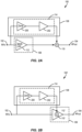
Figure 2A is a more detailed diagram of the amplifier module ofFigure 1 with noise cancellation circuitry and distortion cancellation circuitry illustrated in the second path along with a summation point after the LNA stage; -
Figure 2B is a more detailed diagram of the amplifier module ofFigure 1 with noise cancellation circuitry and distortion cancellation circuitry illustrated in the second path along with a summation point within the LNA stage; -
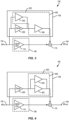
Figure 3 is a more detailed diagram of the amplifier module ofFigure 2A with two distortion cancellation circuits in series to cancel second and third order distortion; -
Figure 4 is a more detailed diagram of the amplifier module ofFigure 2A with two distortion cancellation circuits in parallel to cancel second and third order distortion; -
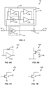
Figure 5 is a more detailed diagram of the amplifier module ofFigure 2A with three distortion cancellation circuits to cancel second and third order distortion; -
Figure 6A is a first example aspect of a noise cancellation circuit; -
Figure 6B is a second example aspect of a noise cancellation circuit; -
Figure 7A is a first example aspect of a distortion cancellation circuit; -
Figure 7B is a second example aspect of a distortion cancellation circuit; -
Figure 8 is a block diagram of the amplifier module ofFigure 2B showing how an interior summation may be arranged; -
Figure 9 is a circuit diagram of the amplifier module ofFigure 3 provided to facilitate how such a structure may be instantiated; -
Figure 10 is a block diagram of an example aspect where additional distortion cancellation is provided by a cascode element within the LNA stage; -
Figure 11 is a block diagram of an alternate aspect of the amplifier module ofFigure 8 with current reuse highlighted; and -
Figure 12 is a block diagram showing details of an inductor-based summation circuit for the amplifier module ofFigure 2A . - The embodiments set forth below represent the necessary information to enable those skilled in the art to practice the embodiments and illustrate the best mode of practicing the embodiments. Upon reading the following description in light of the accompanying drawing figures, those skilled in the art will understand the concepts of the disclosure and will recognize applications of these concepts not particularly addressed herein. It should be understood that these concepts and applications fall within the scope of the disclosure and the accompanying claims.
- It will be understood that although the terms first, second, etc. may be used herein to describe various elements, these elements should not be limited by these terms. These terms are only used to distinguish one element from another. For example, a first element could be termed a second element, and similarly, a second element could be termed a first element without departing from the scope of the present disclosure. As used herein, the term "and/or" includes any and all combinations of one or more of the associated listed items.
- It will be understood that when an element such as a layer, region, or substrate is referred to as being "on" or extending "onto" another element, it can be directly on or extend directly onto the other element, or intervening elements may also be present. In contrast, no intervening elements are present when an element is referred to as being "directly on" or extending "directly onto" another element. Likewise, it will be understood that when an element such as a layer, region, or substrate is referred to as being "over" or extending "over" another element, it can be directly over or extend directly over the other element, or intervening elements may also be present. In contrast, no intervening elements are present when an element is referred to as being "directly over" or extending "directly over" another element. It will also be understood that when an element is referred to as being "connected" or "coupled" to another element, it can be directly connected or coupled to the other element, or intervening elements may be present. In contrast, no intervening elements are present when an element is referred to as being "directly connected" or "directly coupled" to another element.
- Relative terms such as "below" or "above" or "upper" or "lower" or "horizontal" or "vertical" may be used herein to describe a relationship of one element, layer, or region to another element, layer, or region as illustrated in the Figures. It will be understood that these terms and those discussed above are intended to encompass different orientations of the device in addition to the orientation depicted in the Figures.
- The terminology used herein is for the purpose of describing particular embodiments only and is not intended to be limiting of the disclosure. As used herein, the singular forms "a," "an," and "the" are intended to include the plural forms as well unless the context clearly indicates otherwise. It will be further understood that the terms "comprises," "comprising," "includes," and/or "including," when used herein, specify the presence of stated features, integers, steps, operations, elements, and/or components, but do not preclude the presence or addition of one or more other features, integers, steps, operations, elements, components, and/or groups thereof.
- Unless otherwise defined, all terms (including technical and scientific terms) used herein have the same meaning as commonly understood by one of ordinary skill in the art to which this disclosure belongs. It will be further understood that terms used herein should be interpreted as having a meaning that is consistent with their meaning in the context of this specification and the relevant art and will not be interpreted in an idealized or overly formal sense unless expressly so defined herein.
- Aspects disclosed in the detailed description include low noise amplifiers (LNAs) with distortion and noise cancellation. In an example aspect, an LNA may have distortion cancellation that is orthogonally implemented relative to noise cancellation such that changes to the distortion cancellation do not affect the noise cancellation. In further example aspects, cancellation circuitry is added in parallel to a main or primary LNA path. The cancellation circuitry may include an initial impedance matching amplifier that effectuates noise cancellation and a second amplifier that effectuates distortion cancellation. Variations in the placement and composition of the second amplifier are provided. By providing a second path that allows for independent control of noise and distortion cancellation, overall performance of the LNA is improved.
- It should be appreciated that normally an LNA has desired performance characteristics with "low noise," generally linear operation over the frequencies of interest, and a generally low-power use profile (particularly for mobile computing applications). Competing against these desired performance characteristics are the inherent non-linearities and noise of the transistors used to provide the main amplification within the LNA. Traditional approaches are typically current intensive and use relatively large inductors to compensate for the noise. Such approaches are expensive and may compromise desired power consumption levels. Likewise, such approaches typically compensate for noise at the expense of distortion or vice versa as the compensation circuitry is shared, leading to compromises in cancellation.
- Example aspects of the present disclosure provide an inductor-less technique to provide independent or orthogonal control of circuitry to provide distortion cancellation and noise cancellation. This cancellation circuitry is provided in a path parallel to the main LNA path and may take a variety of configurations.
- In this regard,
Figure 1 is a block diagram of anamplifier module 100 that may operate as an LNA stage within a receive chain of a transceiver or the like. Theamplifier module 100 includes aninput node 102 and anoutput node 104. Theamplifier module 100 further includes a primary, main, orfirst path 106 between theinput node 102 and theoutput node 104. Theamplifier module 100 further includes asecond path 108 between theinput node 102 and theoutput node 104. Thefirst path 106 and thesecond path 108 may be joined at theoutput node 104 through asummation circuit 110. - With continued reference to
Figure 1 , thefirst path 106 may include amain LNA 112. Similarly, thesecond path 108 may includecancellation circuitry 114. The use of thesecond path 108 andcancellation circuitry 114 allows for the elimination of off-chip inductors, thereby saving space and power. Further, the use of thesecond path 108 allows for current reuse, as will be explained in greater detail below. More details are provided in subsequent Figures. - In this regard,
Figure 2A provides some additional detail about thecancellation circuitry 114. Specifically, thecancellation circuitry 114 may include a noise canceling amplifier 200 (also referred to as Zamp in the Figures), which provides impedance matching such that themain LNA 112 presents a standard impedance (e.g., 50 ohms(Ω)) at theinput node 102. Thecancellation circuitry 114 may further include adistortion canceling amplifier 202, which may provide opposite sign distortion relative to themain LNA 112. As withFigure 1 , thesummation circuit 110 occurs after themain LNA 112. - In contrast,
Figure 2B illustrates an alternate amplifier module 100' where a summation circuit 110' is provided within the circuitry of the main LNA 112'. More detail about this possible configuration is provided below with reference toFigure 8 . This use of thefirst path 106 and thesecond path 108 is consistent with the theories of the present disclosure. -
Figure 3 provides more detail about theamplifier module 100. Specifically, thesecond path 108 may include thenoise canceling amplifier 200 as previously described. Thedistortion canceling amplifier 202 is instantiated by a distortion cancelingamplifier chain 300 having a firstdistortion canceling amplifier 302 electrically in series with a seconddistortion canceling amplifier 304. In a first example aspect, the firstdistortion canceling amplifier 302 may cancel second order distortion from themain LNA 112, and the seconddistortion canceling amplifier 304 may cancel third order distortion from themain LNA 112. While it is contemplated that the firstdistortion canceling amplifier 302 may cancel second order distortion, the firstdistortion canceling amplifier 302 may instead cancel third order distortion, and the seconddistortion canceling amplifier 304 cancel second order distortion. By having twodistortion canceling amplifiers noise canceling amplifier 200. -
Figure 4 provides another example of thesecond path 108. Thedistortion canceling amplifier 202 is instantiated by a distortion cancelingamplifier chain 400 having a firstdistortion canceling amplifier 402 electrically in parallel with a seconddistortion canceling amplifier 404. In a first example aspect, the firstdistortion canceling amplifier 402 may cancel second order distortion from themain LNA 112, and the seconddistortion canceling amplifier 404 may cancel third order distortion from themain LNA 112. -
Figure 5 provides still another example of thesecond path 108. Thedistortion canceling amplifier 202 is instantiated by a distortion cancelingamplifier chain 500, having a firstdistortion canceling amplifier 502 electrically in parallel with a seconddistortion canceling amplifier 504, while both are electrically in series with a thirddistortion canceling amplifier 506. In a first example aspect, the firstdistortion canceling amplifier 502 may cancel third order distortion from themain LNA 112, and the seconddistortion canceling amplifier 504 may cancel second or third order distortion from themain LNA 112. The thirddistortion canceling amplifier 506 may cancel second or third order distortion from themain LNA 112 with the understanding that at least one of the second or thirddistortion canceling amplifiers amplifier chain 500 cancels both second and third order distortion of themain LNA 112. - It should be appreciated that the
noise canceling amplifier 200 may be formed from a variety of different circuits, two of which are set forth asnoise canceling amplifiers Figures 6A and 6B , respectively. Thenoise canceling amplifier 200A is in a shunt feedback arrangement where aresistor 600 provides a feedback loop for ashunt feedback amplifier 602. In contrast, thenoise canceling amplifier 200B is a common gate transistor arrangement where agate 604 is coupled toground 606. It should be appreciated that n-type field effect transistors (FETs) (NFETs) or p-type FETs (PFETs) may be used, or a combination (i.e., complementary) may be used. Likewise, the present disclosure is not limited to a specific material and may be silicon carbide (SiC), gallium arsenide (GaAs), gallium nitride (GaN), silicon (Si), germanium (Ge), or the like. - It should further be appreciated that the
distortion canceling amplifier 202 may likewise be formed from a variety of different circuits, two of which are set forth asdistortion canceling amplifiers Figures 7A and 7B , respectively. Thedistortion canceling amplifier 202A is asource following amplifier 700, while thedistortion canceling amplifier 202B is acommon source amplifier 702. Again, the particular material or type of FET may be varied as needed or desired without departing from the present disclosure. Likewise, any amplifiers discussed herein may be single ended, differential, quadrature, or the like. - In general, to effectuate distortion cancellation, the devices operate at different current levels. That is, a device with a high gain, low noise has a high current density and may be considered strongly inverted. Conversely, a device to cancel such strongly inverted devices should be weakly inverted and have relatively low current density.
-
Figure 8 provides a hybrid view of a specific implementation of anamplifier module 800 based on the amplifier module 100' ofFigure 2B . The main LNA 112' is formed from cascoded amplifiers 802(1)-802(2), with a node 804 therebetween that acts as the summation circuit 110' where currents are summed. More specifically, a cancellation current Icancel is provided by thesecond path 108 to the node 804 and summed with the cascode current of the main LNA 112'. - With continued reference to
Figure 8 , thesecond path 108 includes thenoise canceling amplifier 200B, with thegate 604 coupled toground 606 through abias network 806. Further, the noisedistortion canceling amplifier 200B may be alternating current (AC) coupled through acapacitor 808. Adrain 810 of thenoise canceling amplifier 200B is coupled to avariable Zload 812 and to the gate of thedistortion canceling amplifier 202A. Thedistortion canceling amplifier 202A generates the cancellation current Icancel that is provided to the main LNA 112'. As shown, thenoise canceling amplifier 200B may be in a high inversion state, while thedistortion canceling amplifier 202A is in a weak inversion state. This arrangement also allows the current to be reused between theamplifiers second path 108 is substantially smaller than the current used by the first path 106 (e.g., a 90-10 split being contemplated). This current splitting is desirable because the most current is used to support the signal of interest rather than to cancel noise and distortion. -
Figure 9 is a circuit-level diagram of theamplifier module 100 using the arrangement of the distortion cancelingamplifier chain 300 ofFigure 3 . While a specific circuit is illustrated, it should be appreciated that there are other ways to achieve the same functionality.Figure 9 is included to show possession of a working circuit. - Note that it is also possible to use some of the cascode amplifiers of the
main LNA 112 to provide additional distortion (e.g., third order distortion), as better seen inFigure 10 , where themain LNA 112 includes acascode amplifier 1000 in addition to amain amplifier 1002 and anothercascode amplifier 1004. Thesecond path 108 has anoise canceling amplifier 200 and adistortion canceling amplifier 202, which may, for example, cancel second order distortion. Thecascode amplifier 1000 may also be considered part of thesecond path 108 and may provide additional distortion cancellation. - More current reuse may be provided by changing the noise canceling amplifier from a grounded gate to a floating gate, as is better seen in
Figure 11 . In most regards, theamplifier module 1100 ofFigure 11 is the same as theamplifier module 800 ofFigure 8 , but thegate 604 is also coupled to the summation circuit 110' through acapacitor 1102, thereby forming feedback for the input impedance of thenoise canceling amplifier 200B. By providing this linkage, current is reused within thenoise canceling amplifier 200B, again reducing overall current use by thesecond path 108. Note that an additional cascode amplifier 802(3) may be added without departing from the present disclosure. - While the aspects discussed above have contemplated a
summation circuit 110, 110' that is current summation based, the present disclosure is not so limited. It is also possible to sum through a transformer, as illustrated inFigure 12 . Specifically, apower amplifier module 1200 includes anoise canceling amplifier 200, which may be ashunt feedback amplifier 602 with an additional capacitor 1202 parallel to theresistor 600. Equivalently, theshunt feedback amplifier 602 may be replaced by acircuit 1204. The output from thedistortion canceling amplifier 202B is summed in asummation circuit 110", which is an inverting transformer. Alternatively, thesummation circuit 110" may be replaced withinductors 110‴. - Therefore, from one perspective, there have been described low noise amplifiers (LNAs). In one aspect, an LNA may have distortion cancellation that is orthogonally implemented relative to noise cancellation such that changes to the distortion cancellation do not affect the noise cancellation. In further example aspects, cancellation circuitry is added in parallel to a main or primary LNA path. The cancellation circuitry may include an initial impedance matching amplifier that effectuates noise cancellation and a second amplifier that effectuates distortion cancellation. Variations in the placement and composition of the second amplifier are provided. By providing a second path that allows for independent control of noise and distortion cancellation, overall performance of the LNA is improved.
- Further examples are set out in the following numbered clauses.
-
Clause 1. A power amplifier (PA) module comprising: a first path coupling an input node and an output node, the first path comprising a low noise amplifier (LNA); and a second path coupling the input node and the output node, the second path electrically parallel to the first path, the second path comprising cancellation circuitry comprising: a noise cancellation circuit; and a distortion cancellation circuit. -
Clause 2. The PA module ofclause 1, wherein the noise cancellation circuit comprises a noise canceling amplifier configured to adjust an impedance presented at the input node. -
Clause 3. The PA ofclause 2, wherein the noise canceling amplifier comprises a common gate transistor. - Clause 4. The PA of
clause - Clause 5. The PA of any preceding clause, wherein the distortion cancellation circuit comprises a distortion canceling amplifier electrically serially following the noise cancellation circuit.
- Clause 6. The PA of any preceding clause, wherein the distortion cancellation circuit comprises a first distortion canceling amplifier electrically in parallel with a second distortion canceling amplifier, wherein the first distortion canceling amplifier cancels second order distortion in the LNA and the second distortion canceling amplifier cancels third order distortion in the LNA.
- Clause 7. The PA of clause 6, wherein the distortion cancellation circuit comprises a third distortion canceling amplifier electrically in series with the first and second distortion canceling amplifiers and electrically in parallel with the noise cancellation circuit.
- Clause 8. The PA of any preceding clause, wherein the distortion cancellation circuit comprises a first distortion canceling amplifier electrically in series with a second distortion canceling amplifier, wherein the first distortion canceling amplifier is electrically in parallel with the noise cancellation circuit.
- Clause 9. The PA of any preceding clause, further comprising a summation circuit summing current from the first path with current from the second path.
- Clause 10. The PA of any preceding clause, further comprising a summation circuit within the LNA, the summation circuit summing current from the first path with current from the second path.
- Clause 11. The PA of any preceding clause, wherein the LNA comprises an n-type field effect transistor (FET) (NFET) configured to be biased in a strong inversion.
- Clause 12. The PA of clause 11, wherein the second path comprises one or more p-type FETs (PFETs) configured to be biased in a weak inversion to create opposite sign distortion.
- Clause 13. The PA of clause 11 or 12, wherein the second path uses one or more NFETs biased in a weak inversion to create opposite sign distortion.
- Clause 14. A low noise amplifying system comprising: a first signal path comprising an amplifying path; and a second signal path comprising a cancellation path configured to cancel noise and distortion independently, wherein devices in the amplifying path are configured to create distortion having a first value and a first sign and devices in the second signal path are configured to create distortion having approximately the first value and a second sign opposite the first sign.
- Clause 15. The low noise amplifying system of clause 14, wherein the second signal path comprises two or more separate stages to achieve independent noise and distortion cancellation.
- Clause 16. The low noise amplifying system of clause 14 or 15, wherein the second signal path comprises a first stage configured to cancel second order distortion of the amplifying path and a second stage configured to cancel third order distortion of the amplifying path.
- While not specifically illustrated, aspects of the present disclosure may incorporate some form of temperature compensation to assist in biasing the amplifiers properly. That is, amplifiers may operate differently at different temperatures. Accordingly, having, for example, a bandgap temperature reference may allow operation to be adjusted as needed to maintain desired operation.
- It is also noted that the operational steps described in any of the example aspects herein are described to provide examples and discussion. The operations described may be performed in numerous different sequences other than the illustrated sequences. Furthermore, operations described in a single operational step may actually be performed in a number of different steps. Additionally, one or more operational steps discussed in the example aspects may be combined. It is to be understood that the operational steps illustrated in the flowchart diagrams may be subject to numerous different modifications, as will be readily apparent to one of skill in the art. Those of skill in the art will also understand that information and signals may be represented using any of a variety of different technologies and techniques. For example, data, instructions, commands, information, signals, bits, symbols, and chips that may be referenced throughout the above description may be represented by voltages, currents, electromagnetic waves, magnetic fields or particles, optical fields or particles, or any combination thereof.
- The previous description of the disclosure is provided to enable any person skilled in the art to make or use the disclosure. Various modifications to the disclosure will be readily apparent to those skilled in the art, and the generic principles defined herein may be applied to other variations. Thus, the disclosure is not intended to be limited to the examples and designs described herein but is to be accorded the widest scope consistent with the principles and novel features disclosed herein.
Claims (15)
- A power amplifier (PA) module comprising:a first path coupling an input node and an output node, the first path comprising a low noise amplifier (LNA); anda second path coupling the input node and the output node, the second path electrically parallel to the first path, the second path comprising cancellation circuitry comprising:a noise cancellation circuit; anda distortion cancellation circuit.
- The PA module of claim 1, wherein the noise cancellation circuit comprises a noise canceling amplifier configured to adjust an impedance presented at the input node.
- The PA of claim 2, wherein the noise canceling amplifier comprises a common gate transistor.
- The PA of claim 2 or 3, wherein the noise canceling amplifier comprises a shunt feedback amplifier.
- The PA of any preceding claim, wherein the distortion cancellation circuit comprises a distortion canceling amplifier electrically serially following the noise cancellation circuit.
- The PA of any preceding claim, wherein the distortion cancellation circuit comprises a first distortion canceling amplifier electrically in parallel with a second distortion canceling amplifier, wherein the first distortion canceling amplifier cancels second order distortion in the LNA and the second distortion canceling amplifier cancels third order distortion in the LNA.
- The PA of claim 6, wherein the distortion cancellation circuit comprises a third distortion canceling amplifier electrically in series with the first and second distortion canceling amplifiers and electrically in parallel with the noise cancellation circuit.
- The PA of any preceding claim, wherein the distortion cancellation circuit comprises a first distortion canceling amplifier electrically in series with a second distortion canceling amplifier, wherein the first distortion canceling amplifier is electrically in parallel with the noise cancellation circuit.
- The PA of any preceding claim, further comprising a summation circuit summing current from the first path with current from the second path.
- The PA of any preceding claim, further comprising a summation circuit within the LNA, the summation circuit summing current from the first path with current from the second path.
- The PA of any preceding claim, wherein the LNA comprises an n-type field effect transistor (FET) (NFET) configured to be biased in a strong inversion.
- The PA of claim 11, wherein the second path comprises one or more p-type FETs (PFETs) configured to be biased in a weak inversion to create opposite sign distortion and/or uses one or more NFETs biased in a weak inversion to create opposite sign distortion.
- A low noise amplifying system comprising:a first signal path comprising an amplifying path; anda second signal path comprising a cancellation path configured to cancel noise and distortion independently,wherein devices in the amplifying path are configured to create distortion having a first value and a first sign and devices in the second signal path are configured to create distortion having approximately the first value and a second sign opposite the first sign.
- The low noise amplifying system of claim 13, wherein the second signal path comprises two or more separate stages to achieve independent noise and distortion cancellation.
- The low noise amplifying system of claim 13 or 14, wherein the second signal path comprises a first stage configured to cancel second order distortion of the amplifying path and a second stage configured to cancel third order distortion of the amplifying path.
Applications Claiming Priority (5)
| Application Number | Priority Date | Filing Date | Title |
|---|---|---|---|
| US202263342678P | 2022-05-17 | 2022-05-17 | |
| US202263400502P | 2022-08-24 | 2022-08-24 | |
| US202263375064P | 2022-09-09 | 2022-09-09 | |
| US18/298,426 US12633880B2 (en) | 2023-04-11 | Inductorless self-tuned input-matching low-noise amplifier with very low noise figure and Gm boost | |
| US18/133,143 US12562696B2 (en) | 2022-05-17 | 2023-04-11 | Low noise amplifier (LNA) with distortion and noise cancellation |
Publications (1)
| Publication Number | Publication Date |
|---|---|
| EP4280456A1 true EP4280456A1 (en) | 2023-11-22 |
Family
ID=86330758
Family Applications (1)
| Application Number | Title | Priority Date | Filing Date |
|---|---|---|---|
| EP23174050.7A Pending EP4280456A1 (en) | 2022-05-17 | 2023-05-17 | Low noise amplifier (lna) with distortion and noise cancellation |
Country Status (2)
| Country | Link |
|---|---|
| US (1) | US12562696B2 (en) |
| EP (1) | EP4280456A1 (en) |
Families Citing this family (2)
| Publication number | Priority date | Publication date | Assignee | Title |
|---|---|---|---|---|
| WO2025170495A1 (en) * | 2024-02-07 | 2025-08-14 | Telefonaktiebolaget Lm Ericsson (Publ) | Low-noise amplifier circuit for full-duplex transceiver |
| CN118868810B (en) * | 2024-09-26 | 2024-12-31 | 合肥灿芯科技有限公司 | Novel dual-mode low-noise amplifier |
Citations (2)
| Publication number | Priority date | Publication date | Assignee | Title |
|---|---|---|---|---|
| US20180298426A1 (en) | 2013-03-14 | 2018-10-18 | Gen-Probe Incorporated | Systems and methods for performing assays |
| US10903798B2 (en) * | 2018-01-04 | 2021-01-26 | Short Circuit Technologies Llc | Ultrawideband very low noise amplifier with noise reduction and current reuse |
Family Cites Families (7)
| Publication number | Priority date | Publication date | Assignee | Title |
|---|---|---|---|---|
| JP4199185B2 (en) | 2004-03-01 | 2008-12-17 | パナソニック株式会社 | Transmitting apparatus and wireless communication apparatus |
| GB2442773A (en) | 2006-10-11 | 2008-04-16 | Tandberg Television Asa | Canceling distortion |
| JP5063528B2 (en) * | 2008-08-21 | 2012-10-31 | 株式会社オーディオテクニカ | Noise cancellation system |
| US8258877B2 (en) | 2009-03-18 | 2012-09-04 | University Of Southern California | Feed-back and feed-forward systems and methods to reduce oscillator phase-noise |
| CN103414439B (en) * | 2013-07-26 | 2016-08-31 | 江苏科技大学 | A Fully Differential Power Current Amplifier with Noise Cancellation Circuit |
| US9524712B2 (en) * | 2014-09-03 | 2016-12-20 | Intel Corporation | Adaptive filtering for wired speaker amplifiers |
| KR102262208B1 (en) | 2019-05-07 | 2021-06-07 | 조선대학교 산학협력단 | Resistive wideband low noise amplifier with noise canceller |
-
2023
- 2023-04-11 US US18/133,143 patent/US12562696B2/en active Active
- 2023-05-17 EP EP23174050.7A patent/EP4280456A1/en active Pending
Patent Citations (2)
| Publication number | Priority date | Publication date | Assignee | Title |
|---|---|---|---|---|
| US20180298426A1 (en) | 2013-03-14 | 2018-10-18 | Gen-Probe Incorporated | Systems and methods for performing assays |
| US10903798B2 (en) * | 2018-01-04 | 2021-01-26 | Short Circuit Technologies Llc | Ultrawideband very low noise amplifier with noise reduction and current reuse |
Non-Patent Citations (2)
| Title |
|---|
| HENG ZHANG ET AL: "Linearization Techniques for CMOS Low Noise Amplifiers: A Tutorial", IEEE TRANSACTIONS ON CIRCUITS AND SYSTEMS I: REGULAR PAPERS, IEEE, US, vol. 58, no. 1, 30 December 2010 (2010-12-30), pages 22 - 36, XP011340986, ISSN: 1549-8328, DOI: 10.1109/TCSI.2010.2055353 * |
| PANG-HSING CHEN ET AL: "A Highly Linear Broadband CMOS LNA with Noise Cancellation", 2012 SPRING CONGRESS ON ENGINEERING AND TECHNOLOGY, IEEE, 27 May 2012 (2012-05-27), pages 1 - 4, XP032473050, ISBN: 978-1-4577-1965-3, DOI: 10.1109/SCET.2012.6342110 * |
Also Published As
| Publication number | Publication date |
|---|---|
| US20230378920A1 (en) | 2023-11-23 |
| US12562696B2 (en) | 2026-02-24 |
Similar Documents
| Publication | Publication Date | Title |
|---|---|---|
| CN105409116B (en) | Amplifier with Configurable Mutual Coupled Source Degeneration Inductor | |
| US12081243B2 (en) | Low noise amplifiers with combined outputs | |
| CN104335483B (en) | Multiple-Input Multiple-Output (MIMO) Low Noise Amplifier for Carrier Aggregation | |
| CN105009448B (en) | Amplifier with multiple outputs and configurable degeneration inductor | |
| CN105009447B (en) | With inductance decline, configurable gain and the matched amplifier of input | |
| JP6272817B2 (en) | Multi-antenna wireless device with power amplifier with different characteristics | |
| US12562696B2 (en) | Low noise amplifier (LNA) with distortion and noise cancellation | |
| CN105103442A (en) | Amplifiers with boosted or deboosted source degeneration inductance | |
| CN105075114A (en) | Split amplifier with improved linearity | |
| EP1418668A1 (en) | High isolation/high speed buffer amplifier | |
| US9509256B2 (en) | Linearized gate capacitance in power amplifiers | |
| KR101543818B1 (en) | Front end for rf transmitting-receiving systems with implicit directional control and time-multiplexing method in submicron technology | |
| CN113644881B (en) | Receiver front-end architecture for in-band carrier aggregation | |
| US12191816B2 (en) | Complementary balanced low-noise amplifier circuit | |
| CN117081510A (en) | Low Noise Amplifier (LNA) with distortion and noise cancellation | |
| HK40098009A (en) | Low noise amplifier (lna) with distortion and noise cancellation | |
| US7332964B2 (en) | Gain-step transconductor | |
| CN119561508A (en) | Unit amplifier circuit, amplifier and receiving circuit |
Legal Events
| Date | Code | Title | Description |
|---|---|---|---|
| PUAI | Public reference made under article 153(3) epc to a published international application that has entered the european phase |
Free format text: ORIGINAL CODE: 0009012 |
|
| STAA | Information on the status of an ep patent application or granted ep patent |
Free format text: STATUS: THE APPLICATION HAS BEEN PUBLISHED |
|
| AK | Designated contracting states |
Kind code of ref document: A1 Designated state(s): AL AT BE BG CH CY CZ DE DK EE ES FI FR GB GR HR HU IE IS IT LI LT LU LV MC ME MK MT NL NO PL PT RO RS SE SI SK SM TR |
|
| STAA | Information on the status of an ep patent application or granted ep patent |
Free format text: STATUS: REQUEST FOR EXAMINATION WAS MADE |
|
| 17P | Request for examination filed |
Effective date: 20240517 |
|
| RBV | Designated contracting states (corrected) |
Designated state(s): AL AT BE BG CH CY CZ DE DK EE ES FI FR GB GR HR HU IE IS IT LI LT LU LV MC ME MK MT NL NO PL PT RO RS SE SI SK SM TR |