EP4280104A1 - Card-type medium and card-type medium manufacturing method - Google Patents
Card-type medium and card-type medium manufacturing method Download PDFInfo
- Publication number
- EP4280104A1 EP4280104A1 EP21919522.9A EP21919522A EP4280104A1 EP 4280104 A1 EP4280104 A1 EP 4280104A1 EP 21919522 A EP21919522 A EP 21919522A EP 4280104 A1 EP4280104 A1 EP 4280104A1
- Authority
- EP
- European Patent Office
- Prior art keywords
- card
- joining material
- conductive joining
- circuit board
- intermediate spacer
- Prior art date
- Legal status (The legal status is an assumption and is not a legal conclusion. Google has not performed a legal analysis and makes no representation as to the accuracy of the status listed.)
- Granted
Links
Images



Classifications
-
- G—PHYSICS
- G06—COMPUTING OR CALCULATING; COUNTING
- G06K—GRAPHICAL DATA READING; PRESENTATION OF DATA; RECORD CARRIERS; HANDLING RECORD CARRIERS
- G06K19/00—Record carriers for use with machines and with at least a part designed to carry digital markings
- G06K19/06—Record carriers for use with machines and with at least a part designed to carry digital markings characterised by the kind of the digital marking, e.g. shape, nature, code
- G06K19/067—Record carriers with conductive marks, printed circuits or semiconductor circuit elements, e.g. credit or identity cards also with resonating or responding marks without active components
- G06K19/07—Record carriers with conductive marks, printed circuits or semiconductor circuit elements, e.g. credit or identity cards also with resonating or responding marks without active components with integrated circuit chips
- G06K19/077—Constructional details, e.g. mounting of circuits in the carrier
- G06K19/07745—Mounting details of integrated circuit chips
-
- B—PERFORMING OPERATIONS; TRANSPORTING
- B42—BOOKBINDING; ALBUMS; FILES; SPECIAL PRINTED MATTER
- B42D—BOOKS; BOOK COVERS; LOOSE LEAVES; PRINTED MATTER CHARACTERISED BY IDENTIFICATION OR SECURITY FEATURES; PRINTED MATTER OF SPECIAL FORMAT OR STYLE NOT OTHERWISE PROVIDED FOR; DEVICES FOR USE THEREWITH AND NOT OTHERWISE PROVIDED FOR; MOVABLE-STRIP WRITING OR READING APPARATUS
- B42D25/00—Information-bearing cards or sheet-like structures characterised by identification or security features; Manufacture thereof
- B42D25/30—Identification or security features, e.g. for preventing forgery
- B42D25/305—Associated digital information
-
- B—PERFORMING OPERATIONS; TRANSPORTING
- B42—BOOKBINDING; ALBUMS; FILES; SPECIAL PRINTED MATTER
- B42D—BOOKS; BOOK COVERS; LOOSE LEAVES; PRINTED MATTER CHARACTERISED BY IDENTIFICATION OR SECURITY FEATURES; PRINTED MATTER OF SPECIAL FORMAT OR STYLE NOT OTHERWISE PROVIDED FOR; DEVICES FOR USE THEREWITH AND NOT OTHERWISE PROVIDED FOR; MOVABLE-STRIP WRITING OR READING APPARATUS
- B42D25/00—Information-bearing cards or sheet-like structures characterised by identification or security features; Manufacture thereof
- B42D25/30—Identification or security features, e.g. for preventing forgery
- B42D25/313—Fingerprints
-
- G—PHYSICS
- G06—COMPUTING OR CALCULATING; COUNTING
- G06K—GRAPHICAL DATA READING; PRESENTATION OF DATA; RECORD CARRIERS; HANDLING RECORD CARRIERS
- G06K19/00—Record carriers for use with machines and with at least a part designed to carry digital markings
- G06K19/06—Record carriers for use with machines and with at least a part designed to carry digital markings characterised by the kind of the digital marking, e.g. shape, nature, code
- G06K19/067—Record carriers with conductive marks, printed circuits or semiconductor circuit elements, e.g. credit or identity cards also with resonating or responding marks without active components
- G06K19/07—Record carriers with conductive marks, printed circuits or semiconductor circuit elements, e.g. credit or identity cards also with resonating or responding marks without active components with integrated circuit chips
- G06K19/0716—Record carriers with conductive marks, printed circuits or semiconductor circuit elements, e.g. credit or identity cards also with resonating or responding marks without active components with integrated circuit chips at least one of the integrated circuit chips comprising a sensor or an interface to a sensor
- G06K19/0718—Record carriers with conductive marks, printed circuits or semiconductor circuit elements, e.g. credit or identity cards also with resonating or responding marks without active components with integrated circuit chips at least one of the integrated circuit chips comprising a sensor or an interface to a sensor the sensor being of the biometric kind, e.g. fingerprint sensors
-
- G—PHYSICS
- G06—COMPUTING OR CALCULATING; COUNTING
- G06K—GRAPHICAL DATA READING; PRESENTATION OF DATA; RECORD CARRIERS; HANDLING RECORD CARRIERS
- G06K19/00—Record carriers for use with machines and with at least a part designed to carry digital markings
- G06K19/06—Record carriers for use with machines and with at least a part designed to carry digital markings characterised by the kind of the digital marking, e.g. shape, nature, code
- G06K19/067—Record carriers with conductive marks, printed circuits or semiconductor circuit elements, e.g. credit or identity cards also with resonating or responding marks without active components
- G06K19/07—Record carriers with conductive marks, printed circuits or semiconductor circuit elements, e.g. credit or identity cards also with resonating or responding marks without active components with integrated circuit chips
- G06K19/077—Constructional details, e.g. mounting of circuits in the carrier
- G06K19/0772—Physical layout of the record carrier
-
- G—PHYSICS
- G06—COMPUTING OR CALCULATING; COUNTING
- G06K—GRAPHICAL DATA READING; PRESENTATION OF DATA; RECORD CARRIERS; HANDLING RECORD CARRIERS
- G06K19/00—Record carriers for use with machines and with at least a part designed to carry digital markings
- G06K19/06—Record carriers for use with machines and with at least a part designed to carry digital markings characterised by the kind of the digital marking, e.g. shape, nature, code
- G06K19/067—Record carriers with conductive marks, printed circuits or semiconductor circuit elements, e.g. credit or identity cards also with resonating or responding marks without active components
- G06K19/07—Record carriers with conductive marks, printed circuits or semiconductor circuit elements, e.g. credit or identity cards also with resonating or responding marks without active components with integrated circuit chips
- G06K19/077—Constructional details, e.g. mounting of circuits in the carrier
- G06K19/0772—Physical layout of the record carrier
- G06K19/07722—Physical layout of the record carrier the record carrier being multilayered, e.g. laminated sheets
-
- G—PHYSICS
- G06—COMPUTING OR CALCULATING; COUNTING
- G06K—GRAPHICAL DATA READING; PRESENTATION OF DATA; RECORD CARRIERS; HANDLING RECORD CARRIERS
- G06K19/00—Record carriers for use with machines and with at least a part designed to carry digital markings
- G06K19/06—Record carriers for use with machines and with at least a part designed to carry digital markings characterised by the kind of the digital marking, e.g. shape, nature, code
- G06K19/067—Record carriers with conductive marks, printed circuits or semiconductor circuit elements, e.g. credit or identity cards also with resonating or responding marks without active components
- G06K19/07—Record carriers with conductive marks, printed circuits or semiconductor circuit elements, e.g. credit or identity cards also with resonating or responding marks without active components with integrated circuit chips
- G06K19/077—Constructional details, e.g. mounting of circuits in the carrier
- G06K19/07743—External electrical contacts
-
- H—ELECTRICITY
- H05—ELECTRIC TECHNIQUES NOT OTHERWISE PROVIDED FOR
- H05K—PRINTED CIRCUITS; CASINGS OR CONSTRUCTIONAL DETAILS OF ELECTRIC APPARATUS; MANUFACTURE OF ASSEMBLAGES OF ELECTRICAL COMPONENTS
- H05K1/00—Printed circuits
- H05K1/02—Details
- H05K1/09—Use of materials for the conductive, e.g. metallic pattern
-
- H—ELECTRICITY
- H05—ELECTRIC TECHNIQUES NOT OTHERWISE PROVIDED FOR
- H05K—PRINTED CIRCUITS; CASINGS OR CONSTRUCTIONAL DETAILS OF ELECTRIC APPARATUS; MANUFACTURE OF ASSEMBLAGES OF ELECTRICAL COMPONENTS
- H05K1/00—Printed circuits
- H05K1/18—Printed circuits structurally associated with non-printed electric components
- H05K1/182—Printed circuits structurally associated with non-printed electric components associated with components mounted in printed circuit boards [PCB], e.g. insert-mounted components [IMC]
- H05K1/183—Printed circuits structurally associated with non-printed electric components associated with components mounted in printed circuit boards [PCB], e.g. insert-mounted components [IMC] associated with components mounted in and supported by recessed areas of the PCBs
-
- H—ELECTRICITY
- H05—ELECTRIC TECHNIQUES NOT OTHERWISE PROVIDED FOR
- H05K—PRINTED CIRCUITS; CASINGS OR CONSTRUCTIONAL DETAILS OF ELECTRIC APPARATUS; MANUFACTURE OF ASSEMBLAGES OF ELECTRICAL COMPONENTS
- H05K1/00—Printed circuits
- H05K1/18—Printed circuits structurally associated with non-printed electric components
- H05K1/182—Printed circuits structurally associated with non-printed electric components associated with components mounted in printed circuit boards [PCB], e.g. insert-mounted components [IMC]
- H05K1/185—Printed circuits structurally associated with non-printed electric components associated with components mounted in printed circuit boards [PCB], e.g. insert-mounted components [IMC] associated with components encapsulated in the insulating substrate of the PCBs; associated with components incorporated in internal layers of multilayer circuit boards
- H05K1/186—Printed circuits structurally associated with non-printed electric components associated with components mounted in printed circuit boards [PCB], e.g. insert-mounted components [IMC] associated with components encapsulated in the insulating substrate of the PCBs; associated with components incorporated in internal layers of multilayer circuit boards manufactured by mounting on or connecting to patterned circuits before or during embedding
-
- H—ELECTRICITY
- H05—ELECTRIC TECHNIQUES NOT OTHERWISE PROVIDED FOR
- H05K—PRINTED CIRCUITS; CASINGS OR CONSTRUCTIONAL DETAILS OF ELECTRIC APPARATUS; MANUFACTURE OF ASSEMBLAGES OF ELECTRICAL COMPONENTS
- H05K2201/00—Indexing scheme relating to printed circuits covered by H05K1/00
- H05K2201/04—Assemblies of printed circuits
- H05K2201/049—PCB for one component, e.g. for mounting onto mother PCB
-
- H—ELECTRICITY
- H05—ELECTRIC TECHNIQUES NOT OTHERWISE PROVIDED FOR
- H05K—PRINTED CIRCUITS; CASINGS OR CONSTRUCTIONAL DETAILS OF ELECTRIC APPARATUS; MANUFACTURE OF ASSEMBLAGES OF ELECTRICAL COMPONENTS
- H05K2201/00—Indexing scheme relating to printed circuits covered by H05K1/00
- H05K2201/20—Details of printed circuits not provided for in H05K2201/01 - H05K2201/10
- H05K2201/2036—Permanent spacer or stand-off in a printed circuit or printed circuit assembly
-
- H—ELECTRICITY
- H05—ELECTRIC TECHNIQUES NOT OTHERWISE PROVIDED FOR
- H05K—PRINTED CIRCUITS; CASINGS OR CONSTRUCTIONAL DETAILS OF ELECTRIC APPARATUS; MANUFACTURE OF ASSEMBLAGES OF ELECTRICAL COMPONENTS
- H05K2203/00—Indexing scheme relating to apparatus or processes for manufacturing printed circuits covered by H05K3/00
- H05K2203/04—Soldering or other types of metallurgic bonding
- H05K2203/047—Soldering with different solders, e.g. two different solders on two sides of the PCB
Definitions
- intermediate spacers are interposed when attaching, to a circuit board embedded in a card body, exposed components such as a contact terminal and a fingerprint sensor that are disposed so as to be partially exposed on a card surface.
- exposed components such as a contact terminal and a fingerprint sensor that are disposed so as to be partially exposed on a card surface.
- the exposed components may be positioned with lower precision due to relative displacement of the exposed components and the intermediate spacers.
- the joint-forming temperature of a joining material can be determined, for example, by conducting various tests on card-type media in which different temperatures have been applied to the joining material and examining whether electrical joining and mechanical joining satisfy predetermined requirements.
- electrical conduction is checked and in addition, tests are conducted based on 5.8 dynamic bending stress and 5.9 dynamic torsional stress specified in JIS X 6305-1 (Identification cards test methods - Part 1: General characteristics) and based on IEC 60749-25 (Semiconductor devices - Mechanical and climatic test methods - Part 25: Temperature cycling).
- the card substrate 401 is formed from an electrically conductive metal material such as stainless steel or a titanium alloy.
- the thickness of the card substrate 401 in the card thickness direction Dt is between 100 ⁇ m and 500 ⁇ m, inclusive, for example.
- the card substrate 401 may be formed of a plastic substrate.
- the circuit board 40 includes a flexible circuit board.
- the circuit board 40 includes a base substrate 40a including insulating materials such as polyethylene terephthalate (PET), polyethylene naphthalate (PEN), polycarbonate (PC), polyimide (PI), and glass epoxy.
- PET polyethylene terephthalate
- PEN polyethylene naphthalate
- PC polycarbonate
- PI polyimide
- glass epoxy glass epoxy
- a predetermined wiring pattern formed of a thin conductive film of aluminum, copper, or the like by etching or the like is disposed on a surface of the base substrate 40a of the circuit board 40.
- a wiring pattern is disposed on a front-surface-10f-side surface of the base substrate 40a, for example.
- connecting electrodes made of copper foils or the like are formed on the front surface and the back surface of an insulating base substrate made of glass epoxy or the like.
- the connecting electrodes on the front surface and the back surface of the intermediate spacer 471 are electrically connected by a through-hole, a via, or the like formed by copper plating or the like.
- the intermediate spacer 471 is electrically connected to the circuit board 40 and the fingerprint sensor 21 via the connecting electrodes.
- the first conductive joining material 451a may be, for example, Ag paste having a joint-forming temperature of 220°C
- the second conductive joining material 451b may be, for example, anisotropic solder having a joint-forming temperature of 180°C or lower.
- the second conductive joining material 451b is the same material as the conductive joining material 450a, which joins the IC chip 31.
- the antenna 50 is formed along a periphery of the circuit board 40 and formed in the shape of a rectangle when viewed in the card thickness direction Dt. A single turn or two or more turns of the antenna 50 are formed along the periphery of the circuit board 40.
- the antenna 50 may be formed, for example, as a portion of the wiring pattern formed on the circuit board 40. Note that the antenna 50 may be separate from the circuit board 40. When the antenna 50 and the circuit board 40 are separate, the antenna 50 may be formed, for example, by positioning a sheet metal, a metallic foil, or a metal line formed into a predetermined antenna shape. In this case, the antenna 50 and the wiring pattern on the circuit board 40 are joined together by soldering, welding, pressure welding, or the like.
- the fingerprint sensor 21, which is relatively likely to be thin is joined to the circuit board 40 using the intermediate spacer 471, and the contact terminal 22, which is relatively likely to be thick, is directly joined to the circuit board 40; thus, each exposed component 20 can be positioned with high precision while the increase in the number of components in the IC card 1 is minimized.
- the combination of the joint-forming temperatures of the conductive joining materials is not limited as long as the combination is appropriate for the combination of manufacturing steps.
- the j oint-forming temperature of the first conductive joining material 451a may be higher than the joint-forming temperature of the second conductive joining material 451b
- the j oint-forming temperature of the second conductive joining material 452b may be higher than the joint-forming temperature of the first conductive joining material 452a.
- the fingerprint sensor 21 is joined to the circuit board 40 in the joining method shown in Fig. 3
- the contact terminal 23 is joined to the circuit board 40 in the joining method shown in Fig. 5 .
Landscapes
- Engineering & Computer Science (AREA)
- Microelectronics & Electronic Packaging (AREA)
- Computer Hardware Design (AREA)
- Physics & Mathematics (AREA)
- General Physics & Mathematics (AREA)
- Theoretical Computer Science (AREA)
- Manufacturing & Machinery (AREA)
- Automation & Control Theory (AREA)
- Combinations Of Printed Boards (AREA)
- Credit Cards Or The Like (AREA)
Abstract
Description
- The present invention relates to card-type media and card-type medium manufacturing methods.
- The present application claims priority to
Japanese Patent Application No. 2021-004389 filed January 14, 2021 - Conventionally, many kinds of card-type media have been developed, such as credit cards, cash cards, prepaid cards, membership cards, gift cards, and membership passes. Furthermore, recent years have seen a growth in popularity of card-type media in which integrated circuit (IC) modules including communication functions are embedded to provide various functions (hereinafter also referred to as "IC cards"). Such IC cards including communication functions also perform contactless communication with a reader/writer using a communication technique involving electromagnetic induction such as radio-frequency identification (RFID).
- In an IC card, a circuit board and elements such as an antenna and an IC module mounted on the circuit board are embedded in a card body. For example, Patent Literature (PTL) 1 discloses a configuration including: a secure element and a fingerprint processing unit that are connected to a flexible circuit board; and a contact pad electrically connected to the secure element. In the configuration disclosed in PTL 1, the contact pad is disposed so as to be exposed on a surface (front surface) of a card body. The contact pad fits into an opening formed in the surface of the card body.
- PTL 1:
JP 2019-511058 A - There are cases where, for the purpose of vertical alignment, intermediate spacers are interposed when attaching, to a circuit board embedded in a card body, exposed components such as a contact terminal and a fingerprint sensor that are disposed so as to be partially exposed on a card surface. However, in such cases, the exposed components may be positioned with lower precision due to relative displacement of the exposed components and the intermediate spacers.
- The present invention has been conceived in view of the aforementioned circumstances and provides a card-type medium having a structure that allows more precise positioning of an exposed component that is attached to a circuit board with an intermediate spacer interposed therebetween, and a method for manufacturing the card-type medium.
- A card-type medium according to an aspect of the present invention includes: a card body; an exposed component that is accommodated inside an opening formed in a front surface of the card body and is disposed so as to be partially exposed on the front surface; and a circuit board that is embedded in the card body and to which the exposed component is attached. The exposed component includes a first exposed component that is attached to the circuit board with an intermediate spacer interposed therebetween. The first exposed component and the intermediate spacer are joined together by a first conductive joining material. The circuit board and the intermediate spacer are joined together by a second conductive joining material. A j oint-forming temperature of the first conductive joining material and a j oint-forming temperature of the second conductive joining material are different from each other.
- A card-type medium manufacturing method according to an aspect of the present invention is a method for manufacturing the above-described card-type medium including a configuration in which the joint-forming temperature of the first conductive joining material is higher than the j oint-forming temperature of the second conductive material. The method includes: joining the first exposed component and the intermediate spacer by the first conductive joining material; and joining, by the second conductive joining material, the circuit board and the intermediate spacer joined to the first exposed component.
- A card-type medium manufacturing method according to an aspect of the present invention is a method for manufacturing the above-described card-type medium including a configuration in which the j oint-forming temperature of the second conductive joining material is higher than the j oint-forming temperature of the first conductive material. The card-type medium manufacturing method includes: joining the circuit board and the intermediate spacer by the second conductive joining material; and joining, by the first conductive joining material, the first exposed component and the intermediate spacer joined to the circuit board.
- According to the above-described aspects of the present invention, it is possible to provide a card-type medium and a card-type medium manufacturing method in which structural components can be stably disposed at desired positions.
-
-
Fig. 1 is an external view of an IC card according to an embodiment of the present invention, when viewed from the front. -
Fig. 2 is a cross-sectional view of the IC card according to the embodiment of the present invention. -
Fig. 3 is a cross-sectional view showing a part of processes according to the embodiment of the present invention in which an exposed component is joined. -
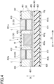
Fig. 4 is a cross-sectional view of an IC card according to a first modification of the embodiment of the present invention. -
Fig. 5 is a cross-sectional view showing a part of processes according to a second modification of the embodiment of the present invention in which an exposed component is joined. - In the present embodiment, a joint-forming temperature of a joining material refers to the minimum temperature at which joining is successful with the joining material. For example, the joint-forming temperature of a metal joining material such as solder is substantially synonymous with the melting point thereof. The joint-forming temperature of a material including conductive particles dispersed in a thermoplastic resin such as anisotropic solder is a temperature depending on the physical properties of the resin and the conductive particles included.
- The joint-forming temperature of a joining material can be determined, for example, by conducting various tests on card-type media in which different temperatures have been applied to the joining material and examining whether electrical joining and mechanical joining satisfy predetermined requirements. In the present embodiment, electrical conduction is checked and in addition, tests are conducted based on 5.8 dynamic bending stress and 5.9 dynamic torsional stress specified in JIS X 6305-1 (Identification cards test methods - Part 1: General characteristics) and based on IEC 60749-25 (Semiconductor devices - Mechanical and climatic test methods - Part 25: Temperature cycling).
- With reference to
Figs. 1 to 5 , an IC card according to an embodiment of the present invention will be described.Fig. 1 is an external view of the IC card according to the embodiment of the present invention, when viewed from the front.Fig. 2 is a cross-sectional view of the IC card according to the embodiment of the present invention. An IC card 1 according to the present embodiment shown inFig. 1 andFig. 2 is a dual interface IC card including acontact terminal 22 which is a contact interface and an antenna 50 (refer toFig. 2 ) which is a contactless interface. Furthermore, the IC card 1 according to the present embodiment includes a biometric authentication function using afingerprint sensor 21. As shown inFig. 1 andFig. 2 , the IC card 1 (the card-type medium) includes acard body 10, an exposedcomponent 20, an encapsulated component 30, acircuit board 40, and anantenna 50. In the present embodiment, the exposedcomponent 20 includes thefingerprint sensor 21 and thecontact terminal 22. - The
card body 10 is in the shape of a plate and formed in the shape of a rectangle when viewed in a card thickness direction Dt (refer toFig. 2 ) orthogonal to afront surface 10f of thecard body 10. The card thickness direction Dt is perpendicular to thefront surface 10f and aback surface 10g of thecard body 10. Note that thefront surface 10f is a surface located at the top inFig. 2 among the surfaces of thecard body 10 in the card thickness direction Dt. Note that theback surface 10g is a surface located at the bottom inFig. 2 among the surfaces of thecard body 10 in the card thickness direction Dt. In the following description, "thefront surface 10f side" refers to an area at the top inFig. 2 , and "theback surface 10g side" refers to an area at the bottom inFig. 2 . - The
card body 10 is formed so that the thickness thereof in the card thickness direction Dt is approximately 0.5 to 1.0 mm, for example. When the IC card 1 is a credit card, thecard body 10 has a thickness of 0.76 mm. As shown inFig. 2 , thecard boy 10 is formed by stacking a plurality of sheet-shaped card substrates - An
opening 410 which accommodates the exposedcomponent 20 is formed in thecard substrate 401 disposed on thefront surface 10f side in thecard body 10. In the present embodiment, twoopenings 410 are formed. Thefingerprint sensor 21 and thecontact terminal 22 are accommodated in theopenings 410. Theopenings 410 are formed penetrating thecard substrate 401 in the card thickness direction Dt. - In the present embodiment, the
card substrate 401 is formed from an electrically conductive metal material such as stainless steel or a titanium alloy. The thickness of thecard substrate 401 in the card thickness direction Dt is between 100 µm and 500 µm, inclusive, for example. Thecard substrate 401 may be formed of a plastic substrate. - In the
card substrate 401, arecess 420 is formed in asubstrate back surface 401g facing theback surface 10g side in the card thickness direction Dt. Therecess 420 is formed so as to be depressed from thesubstrate back surface 401g toward thefront surface 10f in the card thickness direction Dt. The encapsulated component 30 is accommodated in therecess 420. When thecard substrate 401 is formed from a metal material, theopenings 410 and therecess 420 are formed by laser beam machining, cutting, or the like. - The
card substrate 402, which is disposed on theback surface 10g side in thecard body 10, is formed of an insulating plastic substrate including a polyester-based material such as amorphous polyester, a vinyl chloride-based material such as PVC (polyvinyl chloride), a polycarbonate-based material, PET-G (polyethylene terephthalate copolymer), or the like, for example. - An
external resin layer 403 and anexternal resin layer 404 are formed on a front-surface-10f-side surface of thecard substrate 401 and a back-surface-10g-side surface of thecard substrate 402, respectively. Theexternal resin layer 403 forms thefront surface 10f of thecard body 10. Theexternal resin layer 403 forms theback surface 10g of thecard body 10. Theexternal resin layer 403 covers the entire front-surface-10f-side surface of thecard substrate 401 except theopening 410. Theexternal resin layer 404 covers the entire back-surface-10g-side surface of thecard substrate 402. The external resin layers 403, 404 are formed by lamination (of films), for example. - In the present embodiment, the
card substrate 401 and thecard substrate 402 are integrated through converting processes using heat press laminates, adhesives, and the like. Thecard substrate 401 and thecard substrate 402 may be integrated through cold press lamination using a two-component curable resin, a normal temperature curable resin, or a UV (ultraviolet) curable resin. In the present embodiment, aferrite layer 405 is disposed between thecard substrate 401 and thecard substrate 402. - The
circuit board 40 is embedded in thecard body 10. In the present embodiment, thecircuit board 40 is located between thecard substrate 401 and thecard substrate 402 in the card thickness direction Dt. More specifically, thecircuit board 40 is sandwiched between theferrite layer 405 and thecard substrate 402 in the card thickness direction Dt. Although not shown in the drawings, thecircuit board 40 is disposed on the inner side of the outer edge of thecard body 10 when viewed in the card thickness direction Dt. Although not shown in the drawings, thecircuit board 40 has a rectangular outline when viewed in the card thickness direction Dt. The thickness of thecircuit board 40 in the card thickness direction Dt is between 15 µm and 50 µm, inclusive, for example. In the present embodiment, thecircuit board 40 is disposed in a plane orthogonal to the card thickness direction Dt, along a front-surface-10f-side surface of thecard substrate 402 which is disposed on theback surface 10g side in thecard body 10. - In the present embodiment, the
circuit board 40 includes a flexible circuit board. Thecircuit board 40 includes abase substrate 40a including insulating materials such as polyethylene terephthalate (PET), polyethylene naphthalate (PEN), polycarbonate (PC), polyimide (PI), and glass epoxy. Although not shown in the drawings, a predetermined wiring pattern formed of a thin conductive film of aluminum, copper, or the like by etching or the like is disposed on a surface of thebase substrate 40a of thecircuit board 40. In the present embodiment, a wiring pattern is disposed on a front-surface-10f-side surface of thebase substrate 40a, for example. - The encapsulated component 30 is embedded in the
card body 10. In the present embodiment, the IC card 1 includes an IC chip 31 as the encapsulated component 30. The IC chip 31 is joined to aboard front surface 40f of thecircuit board 40 which faces thefront surface 10f side. The IC chip 31 is accommodated in therecess 420. A gap is provided between the IC chip 31 and an inner side surface of therecess 420. In the present embodiment, the IC chip 31 is joined by a conductive joiningmaterial 450a to a front-surface-10f-side surface (theboard front surface 40f) of thecircuit board 40. The conductive joiningmaterial 450a is, for example, anisotropic solder having a joint-forming temperature of 180°C or lower. In the present invention, the anisotropic solder refers to a material in which conductive solder particles are dispersed in a thermoplastic resin. - The IC chip 31 is what is called a secure IC microcomputer and includes, for example: a fingerprint authentication function using the
fingerprint sensor 21; and a communication function that performs external communication via thecontact terminal 22 or theantenna 50. As the IC chip 31, a chip having a known configuration with a contact communication function and a contactless communication function can be used. Although not shown in the drawings, the IC chip 31 is formed in the shape of a rectangle when viewed in the card thickness direction Dt. - The IC chip 31 is electrically connected to the
fingerprint sensor 21, thecontact terminal 22, and theantenna 50 via the wiring pattern formed on thecircuit board 40. Specifically, thecircuit board 40 includes: a fingerprint sensor wiring part that electrically connects the IC chip 31 and thefingerprint sensor 21; a contact terminal wiring part that electrically connects the IC chip 31 and thecontact terminal 22; and an antenna wiring part that electrically connects the IC chip 31 and theantenna 50. - The exposed
component 20 is accommodated inside theopening 410 formed in thefront surface 10f of thecard body 10 and is disposed so as to be partially exposed on thefront surface 10f. As mentioned above, in the present embodiment, the exposedcomponent 20 includes the fingerprint sensor 21 (the first exposed component) and the contact terminal 22 (the second exposed component). Thefingerprint sensor 21 and thecontact terminal 22 are mounted on theboard front surface 40f of thecircuit board 40. In other words, the exposedcomponent 20 is attached to thecircuit board 40. - In the present embodiment, the
fingerprint sensor 21 is the first exposed component that is attached to thecircuit board 40 via anintermediate spacer 471. Thefingerprint sensor 21 is formed in the shape of a rectangle when viewed in the card thickness direction Dt. Although not shown in the drawings, thefingerprint sensor 21 has a configuration in which a protective film is provided so as to cover multiple electrodes. As shown inFig. 1 , thefingerprint sensor 21 is disposed on one side (the RH side) of a center portion of thefront surface 10f of thecard body 10 in a longitudinal direction D1 of thecard body 10. - In the
intermediate spacer 471, connecting electrodes (not shown in the drawings) made of copper foils or the like are formed on the front surface and the back surface of an insulating base substrate made of glass epoxy or the like. The connecting electrodes on the front surface and the back surface of theintermediate spacer 471 are electrically connected by a through-hole, a via, or the like formed by copper plating or the like. Theintermediate spacer 471 is electrically connected to thecircuit board 40 and thefingerprint sensor 21 via the connecting electrodes. - With the
intermediate spacer 471, even when the component thickness of thefingerprint sensor 21 in the card thickness direction Dt and the component thickness of thecontact terminal 22 in the card thickness direction Dt are different, the surface position of thefingerprint sensor 21 in the card thickness direction Dt and the surface position of thecontact terminal 22 in the card thickness direction Dt can be aligned by selecting the height of theintermediate spacer 471. - The
fingerprint sensor 21 and theintermediate spacer 471 are joined together by a first conductive joiningmaterial 451a. Thecircuit board 40 and theintermediate spacer 471 are joined together by a second conductive joiningmaterial 451b. The joint-forming temperature of the first conductive joiningmaterial 451a and the joint-forming temperature of the second conductive joiningmaterial 451b are different from each other. In the present embodiment, the joint-forming temperature of the first conductive joiningmaterial 451a is higher than the joint-forming temperature of the second conductive joiningmaterial 451b. The first conductive joiningmaterial 451a may be, for example, Ag paste having a joint-forming temperature of 220°C, and the second conductive joiningmaterial 451b may be, for example, anisotropic solder having a joint-forming temperature of 180°C or lower. In the present embodiment, the second conductive joiningmaterial 451b is the same material as the conductive joiningmaterial 450a, which joins the IC chip 31. - The joint-forming temperature of the first conductive joining
material 451a is lower than the upper temperature limits of thefingerprint sensor 21 and theintermediate spacer 471 which are joined together. For example, in the present embodiment, when glass epoxy is used for thefingerprint sensor 21 and theintermediate spacer 471, a material having a joint-forming temperature of 250°C or lower is selected as the first conductive joiningmaterial 451a. The joint-forming temperature of the first conductive joiningmaterial 451a is preferably between 200°C and 250°C, inclusive. The joint-forming temperature of the second conductive joiningmaterial 451b is lower than the upper temperature limit of thecircuit board 40. The joint-forming temperature of the second conductive joiningmaterial 451b may be, for example, between 120°C and 180°C, inclusive. The joint-forming temperature of the second conductive joiningmaterial 451b is preferably between 120°C and 170°C, inclusive. The difference between the joint-forming temperature of the first conductive joiningmaterial 451a and the joint-forming temperature of the second conductive joiningmaterial 451b may be, for example, 20°C or higher. The difference between the j oint-forming temperature of the first conductive joiningmaterial 451a and the joint-forming temperature of the second conductive joiningmaterial 451b is preferably 30°C or higher. - Furthermore, card dimensions are specified in standards; for example, when the IC card 1 is a credit card, the thickness of the
card body 10 is 0.76 mm. Therefore, there are appropriate ranges for the thickness of the first conductive joiningmaterial 451a and the thickness of the second conductive joiningmaterial 451b. In the present embodiment, the thickness of the first conductive joiningmaterial 451a is preferably between 5 µm and 100 µm, inclusive, and the thickness of the second conductive joiningmaterial 451b is preferably between 5 µm and 100 µm, inclusive. - In the present embodiment, the
contact terminal 22 is a second exposed component that is directly joined to thecircuit board 40. Thecontact terminal 22 is formed in the shape of a rectangle when viewed in the card thickness direction Dt. Thecontact terminal 22 can contact and electrically connect to an external contact terminal provided on a contact-type terminal device such as an automated teller machine. Thecontact terminal 22 is obtained by forming, by etching or the like, a conductor pattern on a surface of an insulating substrate made of glass epoxy, polyimide (PI), or the like, and then performing a plating process thereon using nickel, palladium, gold, or the like. In the present embodiment, thecontact terminal 22 is disposed on the other side (the LH side) of the center portion of thefront surface 10f of thecard body 10 in the longitudinal direction D1 along thefront surface 10f of thecard body 10. - In the present embodiment, the
contact terminal 22 is joined by a conductive joiningmaterial 450b to the front-surface-10f-side surface (theboard front surface 40f) of thecircuit board 40. In the present embodiment, the conductive joiningmaterial 450b, which is the same material as the second conductive joiningmaterial 451b, may be, for example, anisotropic solder having a joint-forming temperature of 180°C or lower. - The
fingerprint sensor 21, thecontact terminal 22, and theintermediate spacer 471 are disposed so that a gap C is formed between each of these and the inner peripheral surface of theopening 410. When a metal material is used for thecard body 10, the gap C is set by design so that no electrical short circuit occurs between the exposedcomponent 20, theintermediate spacer 471, each of the conductive joining materials, and thecard body 10. - The
antenna 50 is formed along a periphery of thecircuit board 40 and formed in the shape of a rectangle when viewed in the card thickness direction Dt. A single turn or two or more turns of theantenna 50 are formed along the periphery of thecircuit board 40. Theantenna 50 may be formed, for example, as a portion of the wiring pattern formed on thecircuit board 40. Note that theantenna 50 may be separate from thecircuit board 40. When theantenna 50 and thecircuit board 40 are separate, theantenna 50 may be formed, for example, by positioning a sheet metal, a metallic foil, or a metal line formed into a predetermined antenna shape. In this case, theantenna 50 and the wiring pattern on thecircuit board 40 are joined together by soldering, welding, pressure welding, or the like. - Next, a method for manufacturing the IC card 1 according to the present embodiment will be described.
Fig. 3 is a cross-sectional view showing a part of processes in which thefingerprint sensor 21 as the first exposed component is joined. The method for manufacturing the IC card 1 according to the present embodiment includes: a first joining step for joining thefingerprint sensor 21 and theintermediate spacer 471 together by the first conductive joiningmaterial 451a; and a second joining step for joining together, by the second conductive joiningmaterial 451b, thecircuit board 40 and theintermediate spacer 471 joined to thefingerprint sensor 21. Specifically, after a step (upstream process) in which thefingerprint sensor 21 and theintermediate spacer 471 are joined together by the first conductive joiningmaterial 451a is performed, a step (downstream process) in which theintermediate spacer 471 and thecircuit board 40 are joined together by the second conductive joiningmaterial 451b is performed. - As shown in
Fig. 3 , in the second joining step, a joined body obtained by joining thefingerprint sensor 21 and theintermediate spacer 471 moves toward thecircuit board 40 from above, and thus theintermediate spacer 471 is joined to theboard front surface 40f. Theintermediate spacer 471 and theboard front surface 40f are joined together using the second conductive joiningmaterial 451b. Theintermediate spacer 471 and theboard front surface 40f are brought into contact with each other via the second conductive joiningmaterial 451b heated into a state in which a joint can be formed, and then when the second conductive joiningmaterial 451b is cured, theintermediate spacer 471 and theboard front surface 40f are thereby joined together. - At the time of joining the
intermediate spacer 471 and thecircuit board 40 together by the second conductive joiningmaterial 451b, heat needs to be applied to change the second conductive joiningmaterial 451b into the state in which a joint can be formed. Therefore, conventionally, with the heat applied at the time of joining theintermediate spacer 471 and thecircuit board 40, the first conductive joiningmaterial 451a for joining thefingerprint sensor 21 and theintermediate spacer 471 may be at least partially melted, which may result in displacement of thefingerprint sensor 21 and theintermediate spacer 471. Thus, thefingerprint sensor 21 may be placed offset relative to thecircuit board 40. - Regarding this issue, in the IC card 1 according to the present embodiment, the
fingerprint sensor 21 as the first exposed component and theintermediate spacer 471 are joined together by the first conductive joiningmaterial 451a, thecircuit board 40 and theintermediate spacer 471 are joined together by the second conductive joiningmaterial 451b, and the j oint-forming temperature of the first conductive joiningmaterial 451a and the joint-forming temperature of the second conductive joiningmaterial 451b are different from each other. Therefore, the upstream process is performed first in which out of the first conductive joiningmaterial 451a and the second conductive joiningmaterial 451b, a conductive joining material having a higher joint-forming temperature is used for joining, followed by the downstream process in which out of the first conductive joiningmaterial 451a and the second conductive joiningmaterial 451b, a conductive joining material having a lower joint-forming temperature is used for joining. This allows the downstream process to be performed at a temperature lower than the temperature required in the upstream process to achieve joining with the conductive joining material. Therefore, for example, the conductive joining material used for the joining in the upstream process can be kept from being melted when heat is applied in the downstream process. Thus, for example, the joint between members joined in the upstream process can be kept from becoming loose or disengaged even when heat is applied in the downstream process. This means that in the downstream process in which the conductive joining material having a lower joint-forming temperature is used, heat is applied so as to reach a temperature at which the conductive joining material having a lower joint-forming temperature changes into the state in which a joint can be formed while the conductive joining material having a higher joint-forming temperature is not melted; thus, a joint can be formed in the downstream process while the joint between the members joined in the upstream process is kept from becoming loose or disengaged. Thus, the downstream process can be performed while the joint formed in the upstream process is maintained, and even when theintermediate spacer 471 is used, relative displacement of the exposedcomponent 20 and theintermediate spacer 471 can be minimized. Therefore, according to the present embodiment, the exposedcomponent 20, which is attached to thecircuit board 40 with theintermediate spacer 471 interposed therebetween, can be positioned with improved precision. Furthermore, since the exposedcomponent 20 can be positioned with improved precision, the interference of the exposedcomponent 20 with the inner side surface of theopening 410 can be minimized. - Specifically, in the IC card 1 according to the present embodiment, the joint-forming temperature of the first conductive joining
material 451a is higher than the joint-forming temperature of the second conductive joiningmaterial 451b. Therefore, as mentioned above, after a step (upstream process) in which thefingerprint sensor 21 as the first exposed component and theintermediate spacer 471 are joined together by the first conductive joiningmaterial 451a is performed, a step (downstream process) in which theintermediate spacer 471 joined to thefingerprint sensor 21 and thecircuit board 40 are joined together by the second conductive joiningmaterial 451b is performed; thus, theintermediate spacer 471 and thecircuit board 40 can be joined together by the second conductive joiningmaterial 451b while the joint between thefingerprint sensor 21 and theintermediate spacer 471 is kept from becoming loose or disengaged. Thus, thefingerprint sensor 21 upon attachment can be kept from being displaced relative to thecircuit board 40. Therefore, thefingerprint sensor 21, which is attached to thecircuit board 40 with theintermediate spacer 471 interposed therebetween, can be positioned with improved precision. Furthermore, in the downstream process, thefingerprint sensor 21 and theintermediate spacer 471 can be handled as one component to be mounted; therefore, thefingerprint sensor 21 can be easily mounted relative to thecircuit board 40. - The difference between the joint-forming temperature of the first conductive joining
material 451a and the joint-forming temperature of the second conductive joiningmaterial 451b may be, for example, 20°C or higher. The difference between the joint-forming temperature of the first conductive joiningmaterial 451a and the joint-forming temperature of the second conductive joiningmaterial 451b is preferably 30°C or higher. When two different conductive joining materials having such a temperature difference is used, the temperature to be applied to form a joint in the downstream process can be set sufficiently lower than the joint-forming temperature of the first conductive joiningmaterial 451a. Therefore, heating of the second conductive joiningmaterial 451b has less impact on the first conductive joiningmaterial 451a. Thus, for example, the joint between the members joined in the upstream process can be more favorably kept from becoming loose or disengaged even when heat is applied in the downstream process to form a joint using the second conductive joiningmaterial 451b. - In the IC card 1 according to the present embodiment, the exposed
component 20 includes thecontact terminal 22 as the second exposed component that is directly joined to thecircuit board 40. In other words, in the present embodiment, a portion of the exposedcomponent 20 is attached to thecircuit board 40 without using theintermediate spacer 471. Therefore, the total number of components and the number of steps at the time of manufacture can be set smaller than when theintermediate spacer 471 is used for every exposedcomponent 20. - In the IC card 1 according to the present embodiment, the first exposed component includes the
fingerprint sensor 21, and the second exposed component includes thecontact terminal 22. Thefingerprint sensor 21 is more likely to be thinner than thecontact terminal 22. Therefore, theintermediate spacer 471 is likely to be required to vertically align thefingerprint sensor 21 and thecontact terminal 22. Regarding this issue, in the present embodiment, as mentioned above, thefingerprint sensor 21 can be kept from being displaced even when theintermediate spacer 471 is used, and thus thefingerprint sensor 21 can be positioned with high precision. Thus, when the first exposed component is thefingerprint sensor 21, the aforementioned advantageous effect of being able to position the exposedcomponent 20 with improved precision can be more useful. - In contrast, the
contact terminal 22 is more likely to be thicker than thefingerprint sensor 21. Therefore, even when theintermediate spacer 471 is not used in attaching thecontact terminal 22 to thecircuit board 40, thecontact terminal 22 can be easily vertically aligned with thefingerprint sensor 21 attached to thecircuit board 40 with theintermediate spacer 471 interposed therebetween. Therefore, theintermediate spacer 471 need not be used for thecontact terminal 22, and the increase in the number of components in the IC card 1 can be minimized. - As described above, the
fingerprint sensor 21, which is relatively likely to be thin, is joined to thecircuit board 40 using theintermediate spacer 471, and thecontact terminal 22, which is relatively likely to be thick, is directly joined to thecircuit board 40; thus, each exposedcomponent 20 can be positioned with high precision while the increase in the number of components in the IC card 1 is minimized. -
Fig. 4 is a cross-sectional view of an IC card 2 according to a first modification. - In the above-described embodiment, the
fingerprint sensor 21 is joined to thecircuit board 40 with theintermediate spacer 471 interposed therebetween, and thecontact terminal 22 is directly joined to thecircuit board 40; however, how the exposed components is joined is not limited to this embodiment. Acontact terminal 23 may also be attached to thecircuit board 40 with anintermediate spacer 472 interposed therebetween, as shown inFig. 4 . In other words, the exposedcomponent 20 is not required to include the second exposed component that is directly joined to thecircuit board 40. In the present modification, thecontact terminal 23 is the first exposed component. The other features of thecontact terminal 23 are the same as those of thecontact terminal 22. Theintermediate spacer 472 is substantially the same as theintermediate spacer 471 used for thefingerprint sensor 21, for example. - In the present modification, the
contact terminal 23 is joined to theintermediate spacer 472 by a first conductive joiningmaterial 452a, as shown inFig. 4 . Furthermore, theintermediate spacer 472 is joined to thecircuit board 40 by a second conductive joiningmaterial 452b. In the present modification, the joint-forming temperature of the first conductive joiningmaterial 452a is higher than the joint-forming temperature of the second conductive joiningmaterial 452b. Therefore, using a joining method that is substantially the same as a method for joining thefingerprint sensor 21 described in the above embodiment, thecontact terminal 23, which is attached to thecircuit board 40 with theintermediate spacer 472 interposed therebetween, can be positioned with improved precision. - The first conductive joining
material 452a is, for example, the same material as the first conductive joiningmaterial 451a, which joins thefingerprint sensor 21 and theintermediate spacer 471 together. The second conductive joiningmaterial 452b is, for example, the same material as the second conductive joiningmaterial 451b, which joins theintermediate spacer 471 and thecircuit board 40 together. Note that the first conductive joiningmaterial 452a may be a material different from the first conductive joiningmaterial 451a and may have a j oint-forming temperature different from the joint-forming temperature of the first conductive joiningmaterial 451a. The second conductive joiningmaterial 452b may be a material different from the second conductive joiningmaterial 451b and may have a j oint-forming temperature different from the j oint-forming temperature of the second conductive joiningmaterial 451b. - With these
intermediate spacers fingerprint sensor 21 in the card thickness direction Dt and the component thickness of thecontact terminal 23 in the card thickness direction Dt are different, the surface position of thefingerprint sensor 21 in the card thickness direction Dt and the surface position of thecontact terminal 23 in the card thickness direction Dt can be favorably aligned by selecting the height of each of theintermediate spacers -
Fig. 5 is a cross-sectional view showing a part of processes according to a second modification in which thefingerprint sensor 21 as the first exposed component is joined. - In the above embodiment, the joint-forming temperature of the first conductive joining
material 451a is higher than the joint-forming temperature of the second conductive joiningmaterial 451b. However, this is not limiting; the joint-forming temperature of the second conductive joining material may be higher than the joint-forming temperature of the first conductive joining material. - A method for manufacturing an IC card according to the second modification of the present embodiment includes: joining the
circuit board 40 and theintermediate spacer 471 together by a second conductive joiningmaterial 453b; and joining together, by a first conductive joiningmaterial 453a, theintermediate spacer 471 joined to thecircuit board 40 and thefingerprint sensor 21 as the first exposed component, as shown inFig. 5 . Specifically, after a step (upstream process) is performed in which theintermediate spacer 471 and thecircuit board 40 are joined together by the second conductive joiningmaterial 453b, a step (downstream process) is performed in which thefingerprint sensor 21 and theintermediate spacer 471 are joined together by the first conductive joiningmaterial 453a. In these processes, the joint-forming temperature of the second conductive joiningmaterial 453b is higher than the joint-forming temperature of the first conductive joiningmaterial 453a. The first conductive joiningmaterial 453a can be selected in substantially the same manner as the second conductive joiningmaterial 451b described above. The second conductive joiningmaterial 453b can be selected in substantially the same manner as the first conductive joiningmaterial 451a described above. The first conductive joiningmaterial 453a is, for example, anisotropic solder having a joint-forming temperature of 180°C or lower, and the second conductive joiningmaterial 453b is, for example, Ag paste having a joint-forming temperature of 220°C. - As mentioned above, in the present modification, the joint-forming temperature of the second conductive joining
material 453b is higher than the joint-forming temperature of the first conductive joiningmaterial 453a. Therefore, when joining thefingerprint sensor 21 and theintermediate spacer 471 using the first conductive joiningmaterial 453a in the downstream process, even when heat is applied to change the first conductive joiningmaterial 453a into a state in which a joint can be formed, the joint between theintermediate spacer 471 and thecircuit board 40 can be kept from becoming loose or disengaged. Thus, thefingerprint sensor 21 can be kept from being displaced relative to thecircuit board 40, and thefingerprint sensor 21 can be positioned with improved precision. - An embodiment of the present invention has so far been described in detail with reference to the drawings. However, specific configurations are not limited to this embodiment. The present invention should encompass modifications, combinations, or the like of the configurations in the range not departing from the spirit of the present invention.
- For example, the components to be mounted as the encapsulated component 30, the exposed
component 20, and the like are not limited to the IC chip 31, thefingerprint sensor 21, and thecontact terminal 22; other components may be mounted as appropriate. Furthermore, in the above embodiment, two types of the exposedcomponents 20, thefingerprint sensor 21 and thecontact terminal 22, are provided, but this is not limiting. The type, number, etc., of exposedcomponents 20, encapsulated components 30, and the like can be modified accordingly. Furthermore, the card-type medium is exemplified by an IC card 1 which is used as a credit card, but the form and the application thereof are not limited. - The combination of the joint-forming temperatures of the conductive joining materials is not limited as long as the combination is appropriate for the combination of manufacturing steps. For example, in the first modification, the j oint-forming temperature of the first conductive joining
material 451a may be higher than the joint-forming temperature of the second conductive joiningmaterial 451b, and the j oint-forming temperature of the second conductive joiningmaterial 452b may be higher than the joint-forming temperature of the first conductive joiningmaterial 452a. In this case, thefingerprint sensor 21 is joined to thecircuit board 40 in the joining method shown inFig. 3 , and thecontact terminal 23 is joined to thecircuit board 40 in the joining method shown inFig. 5 . - Furthermore, the conductive joining material that directly joins the exposed component and the circuit board and the conductive joining material that directly joins the encapsulated component and the circuit board are not limited to those described in the above embodiment. For example, the conductive joining material that directly joins the exposed component and the like to the circuit board may be the same material as a conductive joining material having a higher joint-forming temperature among the first conductive joining material and the second conductive joining material or may be a material different from both of the first conductive joining material and the second conductive joining material. Furthermore, the conductive joining material having a higher joint-forming temperature is not limited to the Ag paste and may be another material such as an ACF (anisotropic conductive film) or ACP (anisotropic conductive paste), for example. ACF and the ACP are, for example, film-shaped and paste-like materials in which conductive particles are dispersed in a thermoplastic resin. Furthermore, the first conductive joining material and the second conductive joining material may be solder containing only an alloy. In this case, the conductive joining material having a higher joint-possible temperature may be solder having a relatively high melting point, and the conductive joining material having a lower joint-possible temperature may be solder having a relatively low melting point such as low-temperature solder.
-
- 1, 2
- IC card (Card-type medium)
- 10
- Card body
- 10f
- Front surface
- 20
- Exposed component
- 21
- Fingerprint sensor (First exposed component)
- 22
- Contact terminal (Second exposed component)
- 23
- Contact terminal (First exposed component)
- 40
- Circuit board
- 410
- Opening
- 451a, 452a, 453a
- First conductive joining material
- 451b, 452b, 453b
- Second conductive joining material
- 471, 472
- Intermediate spacer
Claims (7)
- A card-type medium comprising:a card body;an exposed component that is accommodated inside an opening formed in a front surface of the card body and is disposed so as to be partially exposed on the front surface; anda circuit board that is embedded in the card body and to which the exposed component is attached, whereinthe exposed component includes a first exposed component that is attached to the circuit board with an intermediate spacer interposed therebetween,the first exposed component and the intermediate spacer are joined together by a first conductive joining material,the circuit board and the intermediate spacer are joined together by a second conductive joining material, anda joint-forming temperature of the first conductive joining material and a joint-forming temperature of the second conductive joining material are different from each other.
- The card-type medium according to claim 1, wherein
the joint-forming temperature of the first conductive joining material is higher than the joint-forming temperature of the second conductive joining material. - The card-type medium according to claim 1, wherein
the j oint-forming temperature of the second conductive joining material is higher than the joint-forming temperature of the first conductive joining material. - The card-type medium according to any one of claims 1 to 3, wherein
the exposed component includes a second exposed component that is directly joined to the circuit board. - The card-type medium according to claim 4, whereinthe first exposed component includes a fingerprint sensor, andthe second exposed component includes a contact terminal.
- A card-type medium manufacturing method for manufacturing the card-type medium according to claim 2, the card-type medium manufacturing method comprising:joining the first exposed component and the intermediate spacer together by the first conductive joining material; andjoining the intermediate spacer joined to the first exposed component and the circuit board together by the second conductive joining material.
- A card-type medium manufacturing method for manufacturing the card-type medium according to claim 3, the card-type medium manufacturing method comprising:joining the circuit board and the intermediate spacer together by the second conductive joining material; andjoining the intermediate spacer joined to the circuit board and the first exposed component together by the first conductive joining material.
Applications Claiming Priority (2)
| Application Number | Priority Date | Filing Date | Title |
|---|---|---|---|
| JP2021004389 | 2021-01-14 | ||
| PCT/JP2021/038130 WO2022153631A1 (en) | 2021-01-14 | 2021-10-14 | Card-type medium and card-type medium manufacturing method |
Publications (3)
| Publication Number | Publication Date |
|---|---|
| EP4280104A1 true EP4280104A1 (en) | 2023-11-22 |
| EP4280104A4 EP4280104A4 (en) | 2024-07-10 |
| EP4280104B1 EP4280104B1 (en) | 2025-11-12 |
Family
ID=82448320
Family Applications (1)
| Application Number | Title | Priority Date | Filing Date |
|---|---|---|---|
| EP21919522.9A Active EP4280104B1 (en) | 2021-01-14 | 2021-10-14 | Card-type medium and card-type medium manufacturing method |
Country Status (5)
| Country | Link |
|---|---|
| US (1) | US12260278B2 (en) |
| EP (1) | EP4280104B1 (en) |
| JP (1) | JP7845197B2 (en) |
| CN (1) | CN116529734A (en) |
| WO (1) | WO2022153631A1 (en) |
Families Citing this family (2)
| Publication number | Priority date | Publication date | Assignee | Title |
|---|---|---|---|---|
| JP7845197B2 (en) * | 2021-01-14 | 2026-04-14 | Toppanホールディングス株式会社 | Card-type media, and method for manufacturing card-type media |
| WO2023095918A1 (en) * | 2021-11-29 | 2023-06-01 | 凸版印刷株式会社 | Inlet and card-type medium |
Family Cites Families (42)
| Publication number | Priority date | Publication date | Assignee | Title |
|---|---|---|---|---|
| JPH0679878B2 (en) * | 1985-09-24 | 1994-10-12 | カシオ計算機株式会社 | IC card |
| US5729150A (en) * | 1995-12-01 | 1998-03-17 | Cascade Microtech, Inc. | Low-current probe card with reduced triboelectric current generating cables |
| KR100309161B1 (en) * | 1999-10-11 | 2001-11-02 | 윤종용 | Memory Card And Method For Making The Same |
| JP2002342731A (en) * | 2001-05-16 | 2002-11-29 | Matsushita Electric Ind Co Ltd | Composite IC card |
| JP2003288573A (en) * | 2002-03-27 | 2003-10-10 | Seiko Epson Corp | IC card and manufacturing method thereof |
| US6686656B1 (en) * | 2003-01-13 | 2004-02-03 | Kingston Technology Corporation | Integrated multi-chip chip scale package |
| JP4412947B2 (en) * | 2003-09-08 | 2010-02-10 | 株式会社ルネサステクノロジ | Memory card |
| JP2006119983A (en) * | 2004-10-22 | 2006-05-11 | Renesas Technology Corp | IC card and manufacturing method thereof |
| JP4097281B2 (en) * | 2006-04-06 | 2008-06-11 | スターエンジニアリング株式会社 | Connection structure between wire-wound coil and IC chip for non-contact ID identification device and connection method constituting the same |
| KR100875952B1 (en) | 2006-09-22 | 2008-12-26 | 소프트픽셀(주) | Electronic card and its manufacturing method |
| US7703661B2 (en) * | 2007-05-23 | 2010-04-27 | International Business Machines Corporation | Method and process for reducing undercooling in a lead-free tin-rich solder alloy |
| KR101523679B1 (en) * | 2009-03-09 | 2015-05-28 | 삼성전자주식회사 | Case for holding a semiconductor memory device and semiconductor memory assembly |
| KR101056435B1 (en) * | 2009-10-05 | 2011-08-11 | 삼성모바일디스플레이주식회사 | Anisotropic conductive film and display device including same |
| US20120069528A1 (en) * | 2010-09-17 | 2012-03-22 | Irvine Sensors Corporation | Method for Control of Solder Collapse in Stacked Microelectronic Structure |
| US9888568B2 (en) * | 2012-02-08 | 2018-02-06 | Crane Electronics, Inc. | Multilayer electronics assembly and method for embedding electrical circuit components within a three dimensional module |
| WO2013142335A1 (en) * | 2012-03-20 | 2013-09-26 | Fry's Metals, Inc. | Solder preforms and solder alloy assembly methods |
| EP2767935A1 (en) * | 2013-02-18 | 2014-08-20 | NagraID S.A. | Plastic layer for electronic card |
| CN105122196B (en) * | 2013-04-18 | 2018-02-06 | 夏普株式会社 | Sensor sheet, sensor sheet assembly, touch-sensing panel assembly and electronic device |
| EP3005589B1 (en) * | 2013-05-24 | 2023-01-18 | Fujifilm Sonosite, Inc. | High frequency ultrasound probe |
| JP6214232B2 (en) * | 2013-06-20 | 2017-10-18 | キヤノン株式会社 | Vibration actuator, replacement lens, imaging device, and automatic stage |
| EP2871596A1 (en) * | 2013-11-12 | 2015-05-13 | Gemalto SA | Interconnected electronic device and method for manufacturing same |
| GB2548639A (en) | 2016-03-24 | 2017-09-27 | Zwipe As | Method of manufacturing a smartcard |
| KR101760675B1 (en) * | 2016-11-09 | 2017-07-24 | 주식회사 마늘랩 | Smart card having middle pad and manufacturing method thereof |
| JPWO2018092897A1 (en) * | 2016-11-18 | 2019-10-17 | 凸版印刷株式会社 | Electromagnetic coupling dual IC card and IC module |
| WO2018187537A1 (en) * | 2017-04-06 | 2018-10-11 | Commscope Technologies Llc | Methods and apparatuses for dispensing solder |
| JP6495368B2 (en) * | 2017-04-19 | 2019-04-03 | 立山科学工業株式会社 | Electronic module |
| JP7204667B2 (en) * | 2017-04-20 | 2023-01-16 | トリナミクス ゲゼルシャフト ミット ベシュレンクテル ハフツング | photodetector |
| US10939544B2 (en) * | 2018-05-10 | 2021-03-02 | Dura Operating, Llc | Multiple resin over-mold for printed circuit board electronics and light guide |
| US10694637B1 (en) * | 2018-09-20 | 2020-06-23 | Rockwell Collins, Inc. | Modular antenna array system with thermal management |
| KR102043102B1 (en) * | 2019-02-20 | 2019-12-02 | (주)비티비엘 | Digital credit card with improved durability |
| KR102043101B1 (en) * | 2019-02-20 | 2019-12-02 | (주)비티비엘 | Digital credit card with improved usability |
| WO2020187720A1 (en) * | 2019-03-15 | 2020-09-24 | Trinamix Gmbh | Optical sensor, method for selecting an optical sensor and detector for optical detection |
| FR3095285B1 (en) * | 2019-04-19 | 2022-11-11 | Linxens Holding | Biometric sensor module for smart card and method of manufacturing such a module |
| JP7309270B2 (en) | 2019-06-25 | 2023-07-18 | 株式会社吉野工業所 | MICROWAVE PLASMA CVD DEVICE, METHOD FOR MANUFACTURING SYNTHETIC RESIN CONTAINER, AND SYNTHETIC RESIN CONTAINER |
| US11755873B1 (en) * | 2020-02-01 | 2023-09-12 | Federal Card Services, LLC | RFID enabled metal transaction cards |
| US12035483B2 (en) * | 2020-04-03 | 2024-07-09 | Dell Products L.P. | Printed circuit board assembly process using multiple solders and assembled boards made using the same |
| EP4258166B1 (en) * | 2020-12-02 | 2025-09-17 | Toppan Inc. | Card medium, electronic component for card medium, and metal card base material for card medium |
| JP7845197B2 (en) * | 2021-01-14 | 2026-04-14 | Toppanホールディングス株式会社 | Card-type media, and method for manufacturing card-type media |
| US20240313121A1 (en) * | 2021-07-21 | 2024-09-19 | Semiconductor Energy Laboratory Co., Ltd. | Semiconductor device |
| US12476214B2 (en) * | 2021-12-21 | 2025-11-18 | Intel Corporation | Solder interconnect hierarchy for heterogeneous electronic device packaging |
| US11895775B2 (en) * | 2022-06-30 | 2024-02-06 | University Of Maryland, College Park | Modular power electronics converters with enhanced connectivity reliability and simplified method of fabrication |
| KR20240018865A (en) * | 2022-08-03 | 2024-02-14 | 삼성전자주식회사 | Fingerprint sensor package and smart card having the same |
-
2021
- 2021-10-14 JP JP2022575082A patent/JP7845197B2/en active Active
- 2021-10-14 WO PCT/JP2021/038130 patent/WO2022153631A1/en not_active Ceased
- 2021-10-14 CN CN202180080277.8A patent/CN116529734A/en active Pending
- 2021-10-14 EP EP21919522.9A patent/EP4280104B1/en active Active
-
2023
- 2023-07-12 US US18/221,279 patent/US12260278B2/en active Active
Also Published As
| Publication number | Publication date |
|---|---|
| WO2022153631A1 (en) | 2022-07-21 |
| JPWO2022153631A1 (en) | 2022-07-21 |
| JP7845197B2 (en) | 2026-04-14 |
| EP4280104B1 (en) | 2025-11-12 |
| US20230359857A1 (en) | 2023-11-09 |
| US12260278B2 (en) | 2025-03-25 |
| CN116529734A (en) | 2023-08-01 |
| EP4280104A4 (en) | 2024-07-10 |
Similar Documents
| Publication | Publication Date | Title |
|---|---|---|
| US20110011939A1 (en) | Contact-less and dual interface inlays and methods for producing the same | |
| JP4241147B2 (en) | IC card manufacturing method | |
| US12260278B2 (en) | Card-type medium and card-type medium manufacturing method | |
| US12579400B2 (en) | Inlet and card medium | |
| US8348170B2 (en) | Method for producing an antenna on a substrate | |
| US12067439B2 (en) | Card-type media | |
| CN108885709B (en) | Method for manufacturing a chip card and a chip card antenna support | |
| CN105512715B (en) | Chip card module arrangement, chip card arrangement and method for producing a chip card arrangement | |
| JP7838486B2 (en) | Card-type media, electronic components for card-type media, and metal card substrates for card-type media. | |
| TWI284842B (en) | Communication medium capable of carrying out contactless communication and method of producing the same | |
| CN113762065A (en) | Biometric sensor module for chip cards and method for producing said module | |
| WO2024029250A1 (en) | Smart card | |
| JP7380254B2 (en) | Contact and non-contact common IC card and contact and non-contact common IC card manufacturing method | |
| JP5701712B2 (en) | RFID antenna sheet, RFID inlet, non-contact IC card, and non-contact IC tag | |
| US20260073175A1 (en) | Ic modules and ic cards | |
| JP7831180B2 (en) | IC card | |
| JP2009157743A (en) | IC non-mounted external connection terminal board type dual IC card | |
| JP2026013311A (en) | Dual interface IC card, intermediate, and method for manufacturing dual interface IC card | |
| JP2010117833A (en) | Inlay, production method thereof, and non-contact type information medium | |
| JP4085790B2 (en) | IC card manufacturing method | |
| JP2026031139A (en) | Dual interface ic card, intermediate body, and method for manufacturing dual interface ic card | |
| HK40065448B (en) | Biometric sensor module for a smart card and method for manufacturing such a module | |
| TWM677396U (en) | Biometric identification cards | |
| JP2023179093A (en) | IC module and IC card |
Legal Events
| Date | Code | Title | Description |
|---|---|---|---|
| STAA | Information on the status of an ep patent application or granted ep patent |
Free format text: STATUS: THE INTERNATIONAL PUBLICATION HAS BEEN MADE |
|
| PUAI | Public reference made under article 153(3) epc to a published international application that has entered the european phase |
Free format text: ORIGINAL CODE: 0009012 |
|
| STAA | Information on the status of an ep patent application or granted ep patent |
Free format text: STATUS: REQUEST FOR EXAMINATION WAS MADE |
|
| 17P | Request for examination filed |
Effective date: 20230614 |
|
| AK | Designated contracting states |
Kind code of ref document: A1 Designated state(s): AL AT BE BG CH CY CZ DE DK EE ES FI FR GB GR HR HU IE IS IT LI LT LU LV MC MK MT NL NO PL PT RO RS SE SI SK SM TR |
|
| DAV | Request for validation of the european patent (deleted) | ||
| DAX | Request for extension of the european patent (deleted) | ||
| A4 | Supplementary search report drawn up and despatched |
Effective date: 20240607 |
|
| RIC1 | Information provided on ipc code assigned before grant |
Ipc: B42D 25/305 20140101ALI20240603BHEP Ipc: G06K 19/077 20060101ALI20240603BHEP Ipc: G06K 19/07 20060101ALI20240603BHEP Ipc: G06K 19/02 20060101AFI20240603BHEP |
|
| STAA | Information on the status of an ep patent application or granted ep patent |
Free format text: STATUS: EXAMINATION IS IN PROGRESS |
|
| 17Q | First examination report despatched |
Effective date: 20250210 |
|
| GRAP | Despatch of communication of intention to grant a patent |
Free format text: ORIGINAL CODE: EPIDOSNIGR1 |
|
| STAA | Information on the status of an ep patent application or granted ep patent |
Free format text: STATUS: GRANT OF PATENT IS INTENDED |
|
| INTG | Intention to grant announced |
Effective date: 20250717 |
|
| GRAS | Grant fee paid |
Free format text: ORIGINAL CODE: EPIDOSNIGR3 |
|
| GRAA | (expected) grant |
Free format text: ORIGINAL CODE: 0009210 |
|
| STAA | Information on the status of an ep patent application or granted ep patent |
Free format text: STATUS: THE PATENT HAS BEEN GRANTED |
|
| AK | Designated contracting states |
Kind code of ref document: B1 Designated state(s): AL AT BE BG CH CY CZ DE DK EE ES FI FR GB GR HR HU IE IS IT LI LT LU LV MC MK MT NL NO PL PT RO RS SE SI SK SM TR |
|
| REG | Reference to a national code |
Ref country code: CH Ref legal event code: F10 Free format text: ST27 STATUS EVENT CODE: U-0-0-F10-F00 (AS PROVIDED BY THE NATIONAL OFFICE) Effective date: 20251112 Ref country code: GB Ref legal event code: FG4D |
|
| REG | Reference to a national code |
Ref country code: IE Ref legal event code: FG4D |
|
| REG | Reference to a national code |
Ref country code: DE Ref legal event code: R096 Ref document number: 602021042453 Country of ref document: DE |
|
| REG | Reference to a national code |
Ref country code: NL Ref legal event code: MP Effective date: 20251112 |
|
| PG25 | Lapsed in a contracting state [announced via postgrant information from national office to epo] |
Ref country code: ES Free format text: LAPSE BECAUSE OF FAILURE TO SUBMIT A TRANSLATION OF THE DESCRIPTION OR TO PAY THE FEE WITHIN THE PRESCRIBED TIME-LIMIT Effective date: 20251112 |
|
| REG | Reference to a national code |
Ref country code: LT Ref legal event code: MG9D |
|
| PG25 | Lapsed in a contracting state [announced via postgrant information from national office to epo] |
Ref country code: NO Free format text: LAPSE BECAUSE OF FAILURE TO SUBMIT A TRANSLATION OF THE DESCRIPTION OR TO PAY THE FEE WITHIN THE PRESCRIBED TIME-LIMIT Effective date: 20260212 |
|
| PG25 | Lapsed in a contracting state [announced via postgrant information from national office to epo] |
Ref country code: HR Free format text: LAPSE BECAUSE OF FAILURE TO SUBMIT A TRANSLATION OF THE DESCRIPTION OR TO PAY THE FEE WITHIN THE PRESCRIBED TIME-LIMIT Effective date: 20251112 Ref country code: AT Free format text: LAPSE BECAUSE OF FAILURE TO SUBMIT A TRANSLATION OF THE DESCRIPTION OR TO PAY THE FEE WITHIN THE PRESCRIBED TIME-LIMIT Effective date: 20251112 Ref country code: FI Free format text: LAPSE BECAUSE OF FAILURE TO SUBMIT A TRANSLATION OF THE DESCRIPTION OR TO PAY THE FEE WITHIN THE PRESCRIBED TIME-LIMIT Effective date: 20251112 |
|
| REG | Reference to a national code |
Ref country code: AT Ref legal event code: MK05 Ref document number: 1857373 Country of ref document: AT Kind code of ref document: T Effective date: 20251112 |
|
| PG25 | Lapsed in a contracting state [announced via postgrant information from national office to epo] |
Ref country code: NL Free format text: LAPSE BECAUSE OF FAILURE TO SUBMIT A TRANSLATION OF THE DESCRIPTION OR TO PAY THE FEE WITHIN THE PRESCRIBED TIME-LIMIT Effective date: 20251112 |
|
| PG25 | Lapsed in a contracting state [announced via postgrant information from national office to epo] |
Ref country code: RS Free format text: LAPSE BECAUSE OF FAILURE TO SUBMIT A TRANSLATION OF THE DESCRIPTION OR TO PAY THE FEE WITHIN THE PRESCRIBED TIME-LIMIT Effective date: 20260212 |
|
| PG25 | Lapsed in a contracting state [announced via postgrant information from national office to epo] |
Ref country code: IS Free format text: LAPSE BECAUSE OF FAILURE TO SUBMIT A TRANSLATION OF THE DESCRIPTION OR TO PAY THE FEE WITHIN THE PRESCRIBED TIME-LIMIT Effective date: 20260312 |
|
| PG25 | Lapsed in a contracting state [announced via postgrant information from national office to epo] |
Ref country code: PT Free format text: LAPSE BECAUSE OF FAILURE TO SUBMIT A TRANSLATION OF THE DESCRIPTION OR TO PAY THE FEE WITHIN THE PRESCRIBED TIME-LIMIT Effective date: 20260312 |
|
| PG25 | Lapsed in a contracting state [announced via postgrant information from national office to epo] |
Ref country code: PL Free format text: LAPSE BECAUSE OF FAILURE TO SUBMIT A TRANSLATION OF THE DESCRIPTION OR TO PAY THE FEE WITHIN THE PRESCRIBED TIME-LIMIT Effective date: 20251112 |
|
| PG25 | Lapsed in a contracting state [announced via postgrant information from national office to epo] |
Ref country code: LV Free format text: LAPSE BECAUSE OF FAILURE TO SUBMIT A TRANSLATION OF THE DESCRIPTION OR TO PAY THE FEE WITHIN THE PRESCRIBED TIME-LIMIT Effective date: 20251112 |
|
| PG25 | Lapsed in a contracting state [announced via postgrant information from national office to epo] |
Ref country code: BG Free format text: LAPSE BECAUSE OF FAILURE TO SUBMIT A TRANSLATION OF THE DESCRIPTION OR TO PAY THE FEE WITHIN THE PRESCRIBED TIME-LIMIT Effective date: 20251112 |
|
| PG25 | Lapsed in a contracting state [announced via postgrant information from national office to epo] |
Ref country code: LT Free format text: LAPSE BECAUSE OF FAILURE TO SUBMIT A TRANSLATION OF THE DESCRIPTION OR TO PAY THE FEE WITHIN THE PRESCRIBED TIME-LIMIT Effective date: 20251112 |
|
| PG25 | Lapsed in a contracting state [announced via postgrant information from national office to epo] |
Ref country code: SM Free format text: LAPSE BECAUSE OF FAILURE TO SUBMIT A TRANSLATION OF THE DESCRIPTION OR TO PAY THE FEE WITHIN THE PRESCRIBED TIME-LIMIT Effective date: 20251112 |
|
| PG25 | Lapsed in a contracting state [announced via postgrant information from national office to epo] |
Ref country code: DK Free format text: LAPSE BECAUSE OF FAILURE TO SUBMIT A TRANSLATION OF THE DESCRIPTION OR TO PAY THE FEE WITHIN THE PRESCRIBED TIME-LIMIT Effective date: 20251112 |
|
| PG25 | Lapsed in a contracting state [announced via postgrant information from national office to epo] |
Ref country code: IT Free format text: LAPSE BECAUSE OF FAILURE TO SUBMIT A TRANSLATION OF THE DESCRIPTION OR TO PAY THE FEE WITHIN THE PRESCRIBED TIME-LIMIT Effective date: 20251112 |
|
| PG25 | Lapsed in a contracting state [announced via postgrant information from national office to epo] |
Ref country code: EE Free format text: LAPSE BECAUSE OF FAILURE TO SUBMIT A TRANSLATION OF THE DESCRIPTION OR TO PAY THE FEE WITHIN THE PRESCRIBED TIME-LIMIT Effective date: 20251112 |
|
| PG25 | Lapsed in a contracting state [announced via postgrant information from national office to epo] |
Ref country code: CZ Free format text: LAPSE BECAUSE OF FAILURE TO SUBMIT A TRANSLATION OF THE DESCRIPTION OR TO PAY THE FEE WITHIN THE PRESCRIBED TIME-LIMIT Effective date: 20251112 |
|
| PG25 | Lapsed in a contracting state [announced via postgrant information from national office to epo] |
Ref country code: SK Free format text: LAPSE BECAUSE OF FAILURE TO SUBMIT A TRANSLATION OF THE DESCRIPTION OR TO PAY THE FEE WITHIN THE PRESCRIBED TIME-LIMIT Effective date: 20251112 |
|
| PG25 | Lapsed in a contracting state [announced via postgrant information from national office to epo] |
Ref country code: SE Free format text: LAPSE BECAUSE OF FAILURE TO SUBMIT A TRANSLATION OF THE DESCRIPTION OR TO PAY THE FEE WITHIN THE PRESCRIBED TIME-LIMIT Effective date: 20251112 |