EP4279481A1 - Compound, hole transport material, and photoelectric conversion element including same - Google Patents
Compound, hole transport material, and photoelectric conversion element including same Download PDFInfo
- Publication number
- EP4279481A1 EP4279481A1 EP22739369.1A EP22739369A EP4279481A1 EP 4279481 A1 EP4279481 A1 EP 4279481A1 EP 22739369 A EP22739369 A EP 22739369A EP 4279481 A1 EP4279481 A1 EP 4279481A1
- Authority
- EP
- European Patent Office
- Prior art keywords
- group
- optionally
- carbon atoms
- substituent
- compound
- Prior art date
- Legal status (The legal status is an assumption and is not a legal conclusion. Google has not performed a legal analysis and makes no representation as to the accuracy of the status listed.)
- Withdrawn
Links
Images
Classifications
-
- C—CHEMISTRY; METALLURGY
- C07—ORGANIC CHEMISTRY
- C07C—ACYCLIC OR CARBOCYCLIC COMPOUNDS
- C07C225/00—Compounds containing amino groups and doubly—bound oxygen atoms bound to the same carbon skeleton, at least one of the doubly—bound oxygen atoms not being part of a —CHO group, e.g. amino ketones
- C07C225/22—Compounds containing amino groups and doubly—bound oxygen atoms bound to the same carbon skeleton, at least one of the doubly—bound oxygen atoms not being part of a —CHO group, e.g. amino ketones having amino groups bound to carbon atoms of six-membered aromatic rings of the carbon skeleton
-
- C—CHEMISTRY; METALLURGY
- C07—ORGANIC CHEMISTRY
- C07C—ACYCLIC OR CARBOCYCLIC COMPOUNDS
- C07C229/00—Compounds containing amino and carboxyl groups bound to the same carbon skeleton
- C07C229/40—Compounds containing amino and carboxyl groups bound to the same carbon skeleton having amino groups bound to carbon atoms of at least one six-membered aromatic ring and carboxyl groups bound to acyclic carbon atoms of the same carbon skeleton
- C07C229/44—Compounds containing amino and carboxyl groups bound to the same carbon skeleton having amino groups bound to carbon atoms of at least one six-membered aromatic ring and carboxyl groups bound to acyclic carbon atoms of the same carbon skeleton with carboxyl groups linked to the six-membered aromatic ring, or to the condensed ring system containing that ring, by unsaturated carbon chains
-
- C—CHEMISTRY; METALLURGY
- C07—ORGANIC CHEMISTRY
- C07C—ACYCLIC OR CARBOCYCLIC COMPOUNDS
- C07C255/00—Carboxylic acid nitriles
- C07C255/01—Carboxylic acid nitriles having cyano groups bound to acyclic carbon atoms
- C07C255/32—Carboxylic acid nitriles having cyano groups bound to acyclic carbon atoms having cyano groups bound to acyclic carbon atoms of a carbon skeleton containing at least one six-membered aromatic ring
- C07C255/42—Carboxylic acid nitriles having cyano groups bound to acyclic carbon atoms having cyano groups bound to acyclic carbon atoms of a carbon skeleton containing at least one six-membered aromatic ring the carbon skeleton being further substituted by singly-bound nitrogen atoms, not being further bound to other hetero atoms
-
- C—CHEMISTRY; METALLURGY
- C07—ORGANIC CHEMISTRY
- C07D—HETEROCYCLIC COMPOUNDS
- C07D209/00—Heterocyclic compounds containing five-membered rings, condensed with other rings, with one nitrogen atom as the only ring hetero atom
- C07D209/56—Ring systems containing three or more rings
- C07D209/80—[b, c]- or [b, d]-condensed
- C07D209/82—Carbazoles; Hydrogenated carbazoles
- C07D209/86—Carbazoles; Hydrogenated carbazoles with only hydrogen atoms, hydrocarbon or substituted hydrocarbon radicals, directly attached to carbon atoms of the ring system
-
- C—CHEMISTRY; METALLURGY
- C07—ORGANIC CHEMISTRY
- C07D—HETEROCYCLIC COMPOUNDS
- C07D209/00—Heterocyclic compounds containing five-membered rings, condensed with other rings, with one nitrogen atom as the only ring hetero atom
- C07D209/56—Ring systems containing three or more rings
- C07D209/80—[b, c]- or [b, d]-condensed
- C07D209/82—Carbazoles; Hydrogenated carbazoles
- C07D209/88—Carbazoles; Hydrogenated carbazoles with hetero atoms or with carbon atoms having three bonds to hetero atoms with at the most one bond to halogen, e.g. ester or nitrile radicals, directly attached to carbon atoms of the ring system
-
- C—CHEMISTRY; METALLURGY
- C07—ORGANIC CHEMISTRY
- C07D—HETEROCYCLIC COMPOUNDS
- C07D239/00—Heterocyclic compounds containing 1,3-diazine or hydrogenated 1,3-diazine rings
- C07D239/02—Heterocyclic compounds containing 1,3-diazine or hydrogenated 1,3-diazine rings not condensed with other rings
- C07D239/24—Heterocyclic compounds containing 1,3-diazine or hydrogenated 1,3-diazine rings not condensed with other rings having three or more double bonds between ring members or between ring members and non-ring members
- C07D239/28—Heterocyclic compounds containing 1,3-diazine or hydrogenated 1,3-diazine rings not condensed with other rings having three or more double bonds between ring members or between ring members and non-ring members with hetero atoms or with carbon atoms having three bonds to hetero atoms with at the most one bond to halogen, directly attached to ring carbon atoms
- C07D239/46—Two or more oxygen, sulphur or nitrogen atoms
- C07D239/60—Three or more oxygen or sulfur atoms
- C07D239/66—Thiobarbituric acids
-
- C—CHEMISTRY; METALLURGY
- C07—ORGANIC CHEMISTRY
- C07D—HETEROCYCLIC COMPOUNDS
- C07D265/00—Heterocyclic compounds containing six-membered rings having one nitrogen atom and one oxygen atom as the only ring hetero atoms
- C07D265/28—1,4-Oxazines; Hydrogenated 1,4-oxazines
- C07D265/34—1,4-Oxazines; Hydrogenated 1,4-oxazines condensed with carbocyclic rings
- C07D265/38—[b, e]-condensed with two six-membered rings
-
- C—CHEMISTRY; METALLURGY
- C07—ORGANIC CHEMISTRY
- C07D—HETEROCYCLIC COMPOUNDS
- C07D279/00—Heterocyclic compounds containing six-membered rings having one nitrogen atom and one sulfur atom as the only ring hetero atoms
- C07D279/10—1,4-Thiazines; Hydrogenated 1,4-thiazines
- C07D279/14—1,4-Thiazines; Hydrogenated 1,4-thiazines condensed with carbocyclic rings or ring systems
- C07D279/18—[b, e]-condensed with two six-membered rings
- C07D279/22—[b, e]-condensed with two six-membered rings with carbon atoms directly attached to the ring nitrogen atom
-
- C—CHEMISTRY; METALLURGY
- C07—ORGANIC CHEMISTRY
- C07D—HETEROCYCLIC COMPOUNDS
- C07D279/00—Heterocyclic compounds containing six-membered rings having one nitrogen atom and one sulfur atom as the only ring hetero atoms
- C07D279/10—1,4-Thiazines; Hydrogenated 1,4-thiazines
- C07D279/14—1,4-Thiazines; Hydrogenated 1,4-thiazines condensed with carbocyclic rings or ring systems
- C07D279/18—[b, e]-condensed with two six-membered rings
- C07D279/22—[b, e]-condensed with two six-membered rings with carbon atoms directly attached to the ring nitrogen atom
- C07D279/24—[b, e]-condensed with two six-membered rings with carbon atoms directly attached to the ring nitrogen atom with hydrocarbon radicals, substituted by amino radicals, attached to the ring nitrogen atom
- C07D279/28—[b, e]-condensed with two six-membered rings with carbon atoms directly attached to the ring nitrogen atom with hydrocarbon radicals, substituted by amino radicals, attached to the ring nitrogen atom with other substituents attached to the ring system
-
- C—CHEMISTRY; METALLURGY
- C07—ORGANIC CHEMISTRY
- C07D—HETEROCYCLIC COMPOUNDS
- C07D333/00—Heterocyclic compounds containing five-membered rings having one sulfur atom as the only ring hetero atom
- C07D333/02—Heterocyclic compounds containing five-membered rings having one sulfur atom as the only ring hetero atom not condensed with other rings
- C07D333/04—Heterocyclic compounds containing five-membered rings having one sulfur atom as the only ring hetero atom not condensed with other rings not substituted on the ring sulphur atom
- C07D333/06—Heterocyclic compounds containing five-membered rings having one sulfur atom as the only ring hetero atom not condensed with other rings not substituted on the ring sulphur atom with only hydrogen atoms, hydrocarbon or substituted hydrocarbon radicals, directly attached to the ring carbon atoms
- C07D333/22—Radicals substituted by doubly bound hetero atoms, or by two hetero atoms other than halogen singly bound to the same carbon atom
-
- C—CHEMISTRY; METALLURGY
- C07—ORGANIC CHEMISTRY
- C07D—HETEROCYCLIC COMPOUNDS
- C07D333/00—Heterocyclic compounds containing five-membered rings having one sulfur atom as the only ring hetero atom
- C07D333/02—Heterocyclic compounds containing five-membered rings having one sulfur atom as the only ring hetero atom not condensed with other rings
- C07D333/04—Heterocyclic compounds containing five-membered rings having one sulfur atom as the only ring hetero atom not condensed with other rings not substituted on the ring sulphur atom
- C07D333/06—Heterocyclic compounds containing five-membered rings having one sulfur atom as the only ring hetero atom not condensed with other rings not substituted on the ring sulphur atom with only hydrogen atoms, hydrocarbon or substituted hydrocarbon radicals, directly attached to the ring carbon atoms
- C07D333/24—Radicals substituted by carbon atoms having three bonds to hetero atoms with at the most one bond to halogen, e.g. ester or nitrile radicals
-
- C—CHEMISTRY; METALLURGY
- C07—ORGANIC CHEMISTRY
- C07D—HETEROCYCLIC COMPOUNDS
- C07D409/00—Heterocyclic compounds containing two or more hetero rings, at least one ring having sulfur atoms as the only ring hetero atoms
- C07D409/14—Heterocyclic compounds containing two or more hetero rings, at least one ring having sulfur atoms as the only ring hetero atoms containing three or more hetero rings
-
- H—ELECTRICITY
- H10—SEMICONDUCTOR DEVICES; ELECTRIC SOLID-STATE DEVICES NOT OTHERWISE PROVIDED FOR
- H10K—ORGANIC ELECTRIC SOLID-STATE DEVICES
- H10K30/00—Organic devices sensitive to infrared radiation, light, electromagnetic radiation of shorter wavelength or corpuscular radiation
- H10K30/10—Organic devices sensitive to infrared radiation, light, electromagnetic radiation of shorter wavelength or corpuscular radiation comprising heterojunctions between organic semiconductors and inorganic semiconductors
- H10K30/15—Sensitised wide-bandgap semiconductor devices, e.g. dye-sensitised TiO2
-
- H—ELECTRICITY
- H10—SEMICONDUCTOR DEVICES; ELECTRIC SOLID-STATE DEVICES NOT OTHERWISE PROVIDED FOR
- H10K—ORGANIC ELECTRIC SOLID-STATE DEVICES
- H10K30/00—Organic devices sensitive to infrared radiation, light, electromagnetic radiation of shorter wavelength or corpuscular radiation
- H10K30/50—Photovoltaic [PV] devices
-
- H—ELECTRICITY
- H10—SEMICONDUCTOR DEVICES; ELECTRIC SOLID-STATE DEVICES NOT OTHERWISE PROVIDED FOR
- H10K—ORGANIC ELECTRIC SOLID-STATE DEVICES
- H10K30/00—Organic devices sensitive to infrared radiation, light, electromagnetic radiation of shorter wavelength or corpuscular radiation
- H10K30/80—Constructional details
- H10K30/84—Layers having high charge carrier mobility
- H10K30/86—Layers having high hole mobility, e.g. hole-transporting layers or electron-blocking layers
-
- H—ELECTRICITY
- H10—SEMICONDUCTOR DEVICES; ELECTRIC SOLID-STATE DEVICES NOT OTHERWISE PROVIDED FOR
- H10K—ORGANIC ELECTRIC SOLID-STATE DEVICES
- H10K85/00—Organic materials used in the body or electrodes of devices covered by this subclass
- H10K85/50—Organic perovskites; Hybrid organic-inorganic perovskites [HOIP], e.g. CH3NH3PbI3
-
- H—ELECTRICITY
- H10—SEMICONDUCTOR DEVICES; ELECTRIC SOLID-STATE DEVICES NOT OTHERWISE PROVIDED FOR
- H10K—ORGANIC ELECTRIC SOLID-STATE DEVICES
- H10K85/00—Organic materials used in the body or electrodes of devices covered by this subclass
- H10K85/60—Organic compounds having low molecular weight
- H10K85/615—Polycyclic condensed aromatic hydrocarbons, e.g. anthracene
-
- H—ELECTRICITY
- H10—SEMICONDUCTOR DEVICES; ELECTRIC SOLID-STATE DEVICES NOT OTHERWISE PROVIDED FOR
- H10K—ORGANIC ELECTRIC SOLID-STATE DEVICES
- H10K85/00—Organic materials used in the body or electrodes of devices covered by this subclass
- H10K85/60—Organic compounds having low molecular weight
- H10K85/631—Amine compounds having at least two aryl rest on at least one amine-nitrogen atom, e.g. triphenylamine
-
- H—ELECTRICITY
- H10—SEMICONDUCTOR DEVICES; ELECTRIC SOLID-STATE DEVICES NOT OTHERWISE PROVIDED FOR
- H10K—ORGANIC ELECTRIC SOLID-STATE DEVICES
- H10K85/00—Organic materials used in the body or electrodes of devices covered by this subclass
- H10K85/60—Organic compounds having low molecular weight
- H10K85/631—Amine compounds having at least two aryl rest on at least one amine-nitrogen atom, e.g. triphenylamine
- H10K85/633—Amine compounds having at least two aryl rest on at least one amine-nitrogen atom, e.g. triphenylamine comprising polycyclic condensed aromatic hydrocarbons as substituents on the nitrogen atom
-
- H—ELECTRICITY
- H10—SEMICONDUCTOR DEVICES; ELECTRIC SOLID-STATE DEVICES NOT OTHERWISE PROVIDED FOR
- H10K—ORGANIC ELECTRIC SOLID-STATE DEVICES
- H10K85/00—Organic materials used in the body or electrodes of devices covered by this subclass
- H10K85/60—Organic compounds having low molecular weight
- H10K85/631—Amine compounds having at least two aryl rest on at least one amine-nitrogen atom, e.g. triphenylamine
- H10K85/636—Amine compounds having at least two aryl rest on at least one amine-nitrogen atom, e.g. triphenylamine comprising heteroaromatic hydrocarbons as substituents on the nitrogen atom
-
- H—ELECTRICITY
- H10—SEMICONDUCTOR DEVICES; ELECTRIC SOLID-STATE DEVICES NOT OTHERWISE PROVIDED FOR
- H10K—ORGANIC ELECTRIC SOLID-STATE DEVICES
- H10K85/00—Organic materials used in the body or electrodes of devices covered by this subclass
- H10K85/60—Organic compounds having low molecular weight
- H10K85/649—Aromatic compounds comprising a hetero atom
- H10K85/654—Aromatic compounds comprising a hetero atom comprising only nitrogen as heteroatom
-
- H—ELECTRICITY
- H10—SEMICONDUCTOR DEVICES; ELECTRIC SOLID-STATE DEVICES NOT OTHERWISE PROVIDED FOR
- H10K—ORGANIC ELECTRIC SOLID-STATE DEVICES
- H10K85/00—Organic materials used in the body or electrodes of devices covered by this subclass
- H10K85/60—Organic compounds having low molecular weight
- H10K85/649—Aromatic compounds comprising a hetero atom
- H10K85/655—Aromatic compounds comprising a hetero atom comprising only sulfur as heteroatom
-
- H—ELECTRICITY
- H10—SEMICONDUCTOR DEVICES; ELECTRIC SOLID-STATE DEVICES NOT OTHERWISE PROVIDED FOR
- H10K—ORGANIC ELECTRIC SOLID-STATE DEVICES
- H10K85/00—Organic materials used in the body or electrodes of devices covered by this subclass
- H10K85/60—Organic compounds having low molecular weight
- H10K85/649—Aromatic compounds comprising a hetero atom
- H10K85/657—Polycyclic condensed heteroaromatic hydrocarbons
- H10K85/6572—Polycyclic condensed heteroaromatic hydrocarbons comprising only nitrogen in the heteroaromatic polycondensed ring system, e.g. phenanthroline or carbazole
-
- H—ELECTRICITY
- H10—SEMICONDUCTOR DEVICES; ELECTRIC SOLID-STATE DEVICES NOT OTHERWISE PROVIDED FOR
- H10K—ORGANIC ELECTRIC SOLID-STATE DEVICES
- H10K85/00—Organic materials used in the body or electrodes of devices covered by this subclass
- H10K85/60—Organic compounds having low molecular weight
- H10K85/649—Aromatic compounds comprising a hetero atom
- H10K85/657—Polycyclic condensed heteroaromatic hydrocarbons
- H10K85/6574—Polycyclic condensed heteroaromatic hydrocarbons comprising only oxygen in the heteroaromatic polycondensed ring system, e.g. cumarine dyes
-
- C—CHEMISTRY; METALLURGY
- C07—ORGANIC CHEMISTRY
- C07C—ACYCLIC OR CARBOCYCLIC COMPOUNDS
- C07C2603/00—Systems containing at least three condensed rings
- C07C2603/02—Ortho- or ortho- and peri-condensed systems
- C07C2603/04—Ortho- or ortho- and peri-condensed systems containing three rings
- C07C2603/06—Ortho- or ortho- and peri-condensed systems containing three rings containing at least one ring with less than six ring members
- C07C2603/10—Ortho- or ortho- and peri-condensed systems containing three rings containing at least one ring with less than six ring members containing five-membered rings
- C07C2603/12—Ortho- or ortho- and peri-condensed systems containing three rings containing at least one ring with less than six ring members containing five-membered rings only one five-membered ring
- C07C2603/18—Fluorenes; Hydrogenated fluorenes
-
- H—ELECTRICITY
- H10—SEMICONDUCTOR DEVICES; ELECTRIC SOLID-STATE DEVICES NOT OTHERWISE PROVIDED FOR
- H10K—ORGANIC ELECTRIC SOLID-STATE DEVICES
- H10K85/00—Organic materials used in the body or electrodes of devices covered by this subclass
- H10K85/60—Organic compounds having low molecular weight
- H10K85/649—Aromatic compounds comprising a hetero atom
- H10K85/657—Polycyclic condensed heteroaromatic hydrocarbons
-
- Y—GENERAL TAGGING OF NEW TECHNOLOGICAL DEVELOPMENTS; GENERAL TAGGING OF CROSS-SECTIONAL TECHNOLOGIES SPANNING OVER SEVERAL SECTIONS OF THE IPC; TECHNICAL SUBJECTS COVERED BY FORMER USPC CROSS-REFERENCE ART COLLECTIONS [XRACs] AND DIGESTS
- Y02—TECHNOLOGIES OR APPLICATIONS FOR MITIGATION OR ADAPTATION AGAINST CLIMATE CHANGE
- Y02E—REDUCTION OF GREENHOUSE GAS [GHG] EMISSIONS, RELATED TO ENERGY GENERATION, TRANSMISSION OR DISTRIBUTION
- Y02E10/00—Energy generation through renewable energy sources
- Y02E10/50—Photovoltaic [PV] energy
- Y02E10/549—Organic PV cells
Definitions
- the present invention relates to a compound, a hole transport material, and a device for converting light into electricity, the device including the hole transport material.
- perovskite solar cells have a perovskite material-containing layer to convert light into electricity.
- perovskite solar cells the development of solar cells having a perovskite material-containing layer to convert light into electricity.
- R 1 to R 20 each independently represent a hydrogen atom, a halogen atom, a carboxyl group, a trimethylsilyl group, a linear or branched alkyl group having 1 to 20 carbon atoms and optionally having a substituent, a linear or branched alkenyl group having 2 to 20 carbon atoms and optionally having a substituent, a cycloalkyl group having 3 to 10 carbon atoms and optionally having a substituent, an alkyloxy group having 1 to 20 carbon atoms and optionally having a substituent, a cycloalkyloxy group having 3 to 10 carbon atoms and optionally having a substituent, an acyl group having 1 to 20 carbon atoms and optionally having a substituent, a thio group having 1 to 18 carbon atoms and optionally having a substituent, an amino group having 1 to 20 carbon atoms and optionally having a substituent, an aromatic hydrocarbon group having 6 to 36 carbon atoms and having
- the compound and the hole transport layer including the compound according to the present invention enable a device for converting light into electricity and a perovskite solar cell that have favorable power conversion efficiency.
- R 1 to R 20 in the general formula (1) each independently represent a hydrogen atom, a halogen atom, a carboxyl group, a trimethylsilyl group, a linear or branched alkyl group having 1 to 20 carbon atoms and optionally having a substituent, a linear or branched alkenyl group having 2 to 20 carbon atoms and optionally having a substituent, a cycloalkyl group having 3 to 10 carbon atoms and optionally having a substituent, an alkyloxy group having 1 to 20 carbon atoms and optionally having a substituent, a cycloalkyloxy group having 3 to 10 carbon atoms and optionally having a substituent, an acyl group having 1 to 20 carbon atoms and optionally having a substituent, a thio group having 1 to 18 carbon atoms and optionally having a substituent, an amino group having 1 to 20 carbon atoms and optionally having a substituent, an aromatic hydrocarbon group having 6 to 36 carbon atoms
- Examples of the "linear or branched alkyl group having 1 to 20 carbon atoms" of the “linear or branched alkyl group having 1 to 20 carbon atoms and optionally having a substituent" represented by R 1 to R 20 include: a methyl group, an ethyl group, an n-propyl group, an isopropyl group, an n-butyl group, an isobutyl group, an s-butyl group, a t-butyl group, an n-pentyl group, an isopentyl group, an n-hexyl group, a 2-ethylhexyl group, a heptyl group, an octyl group, an isooctyl group, a nonyl group, and a decyl group.
- Examples of the "alkoxy group having 1 to 20 carbon atoms" of the "alkoxy group having 1 to 20 carbon atoms and optionally having a substituent" represented by R 1 to R 20 include: a methoxy group, an ethoxy group, a propoxy group, an n-butoxy group, an n-pentyloxy group, an n-hexyloxy group, a heptyloxy group, an octyloxy group, a nonyloxy group, a decyloxy group, an isopropoxy group, an isobutoxy group, an s-butoxy group, a t-butoxy group, an isooctyloxy group, a t-octyloxy group, a phenoxy group, a tolyloxy group, a biphenylyloxy group, a terphenylyloxy group, a naphthyloxy group, an anthryloxy group, a phenanthryloxy group
- Examples of the "thio group having 1 to 18 carbon atoms" of the “thio group having 1 to 18 carbon atoms and optionally having a substituent" represented by R 1 to R 20 include: a methylthio group, an ethylthio group, a propylthio group, a phenylthio group, and a biphenylthio group.
- Examples of the "amino group having 1 to 20 carbon atoms" of the “amino group having 1 to 20 carbon atoms and optionally having a substituent" represented by R 1 to R 20 include: mono-substituted amino groups such as an ethylamino group, an acetylamino group, and a phenylamino group; and di-substituted amino groups such as a diethylamino group, a diphenylamino group, and an acetylphenylamino group.
- Examples of the "aromatic hydrocarbon group having 6 to 36 carbon atoms" of the “aromatic hydrocarbon group having 6 to 36 carbon atoms and optionally having a substituent" represented by R 1 to R 20 include: a phenyl group, a biphenyl group, a terphenyl group, a naphthyl group, a biphenyl group, an anthracenyl group (anthryl group), a phenanthryl group, a fluorenyl group, an indenyl group, a pyrenyl group, a perylenyl group, a fluoranthenyl group, and a triphenylenyl group.
- the aromatic hydrocarbon group encompasses a "fused polycyclic aromatic group".
- a plurality of "substituents" as described above may be contained, and when a plurality of substituents are contained, the substituents may be the same or different. These "substituents” may further have any of the substituents as listed above.
- R 1 to R 20 are, each independently, preferably a hydrogen atom, a linear or branched alkyl group having 1 to 20 carbon atoms and optionally having a substituent, an alkoxy group having 1 to 20 carbon atoms and optionally having a substituent, a thio group having 1 to 18 carbon atoms and optionally having a substituent, or an amino group having 1 to 20 carbon atoms and optionally having a substituent, and more preferably a hydrogen atom or an alkoxy group having 1 to 10 carbon atoms.
- R 1 , R 2 , R 4 , R 5 , R 6 , R 7 , R 9 , R 10 , R 11 , R 12 , R 14 , R 15 , R 16 , R 17 , R 19 , and R 20 are hydrogen atoms, and at the same time, that R 3 , R 8 , R 13 , and R 18 are alkoxy groups having 1 to 10 carbon atoms, in view of favorable power conversion efficiency when used as a hole transport material in a device for converting light into electricity.
- R 1 and R 2 ; R 2 and R 3 ; R 3 and R 4 ; R 4 and R 5 ; R 6 and R 7 ; R 7 and R 8 ; R 8 and R 9 ; R 9 and R 10 ; R 11 and R 12 ; R 12 and R 13 ; R 13 and R 14 ; R 14 and R 15 ; R 16 and R 17 ; R 17 and R 18 ; R 18 and R 19 ; and R 19 and R 20 may be, in each combination, bonded to each other to form a ring via a single bond, an oxygen atom, a sulfur atom, a selenium atom, or a nitrogen atom.
- Y represents an oxygen atom or CR 21 R 22 , where R 21 and R 22 each independently represent a nitrile group, an acyl group having 1 to 10 carbon atoms and optionally having a substituent, or an alkoxycarbonyl group having 1 to 10 carbon atoms and optionally having a substituent, and are preferably electron-withdrawing groups.
- Examples of the "alkoxycarbonyl group having 1 to 10 carbon atoms" of the “alkoxycarbonyl group having 1 to 10 carbon atoms and optionally having a substituent" represented by R 21 and R 22 include a methoxycarbonyl group and an ethoxycarbonyl group.
- One or more hydrogen atoms of the alkyl group in the alkoxycarbonyl group may be replaced with fluorine atoms, and all of the hydrogen atoms may be replaced with fluorine atoms (that is, perfluorinated).
- R 21 and R 22 may be bonded to each other to form a ring via a single bond, an oxygen atom, a sulfur atom, a selenium atom, or a nitrogen atom.
- the ring is preferably an acidic heterocyclic ring such as a barbituric acid ring, a thiobarbituric acid ring, or an indanedione ring.
- Examples of the "linear or branched alkyl group having 1 to 10 carbon atoms and optionally having a substituent" represented by R 23 to R 28 include those having 1 to 10 carbon atoms, among the above-listed examples of the "linear or branched alkyl group having 1 to 20 carbon atoms and optionally having a substituent" represented by R 1 to R 20 .
- Examples of the "cycloalkyl group having 3 to 10 carbon atoms and optionally having a substituent" represented by R 23 to R 28 include those listed above as examples of the "cycloalkyl group having 3 to 10 carbon atoms and optionally having a substituent" represented by R 1 to R 20 .
- Examples of the "heterocyclic group having 5 to 18 ring-forming atoms and optionally having a substituent" represented by R 23 to R 28 include those having 5 to 18 ring-forming atoms, among the above-listed examples of the "heterocyclic group having 5 to 36 ring-forming atoms and optionally having a substituent" represented by R 1 to R 20 .
- R 23 and R 24 ; R 25 and R 26 ; and R 27 and R 28 may be, in each combination, bonded to each other to form a ring via a single bond, an oxygen atom, a sulfur atom, a selenium atom, or a nitrogen atom.
- Z is preferably a sulfur atom.
- n and n in the general formula (2) represent integers of 0 to 2; with the proviso that, when m is 0, n is 1 or 2, and when n is 0, m is 1 or 2. In other words, cases where both m and n are 0 are excluded.
- m is preferably 1.
- n is preferably 0 or 1.
- the group represented by the general formula (2) may be bonded, at its moiety of the phenyl group or at its moiety of the five-membered heterocyclic group, to the fluorenone moiety serving as the central skeleton of the general formula (1).
- the compounds illustrated below are shown with a plurality of hydrogen atoms, carbon atoms, and others omitted.
- the compounds illustrated below each merely represent an exemplar among possible isomers and should be construed to encompass all of the other isomers.
- the compounds each may be a mixture of two or more isomers.
- the compound represented by the general formula (1) may be purified by, for example, column chromatography; adsorption with silica gel, activated carbon, activated clay, or the like; or recrystallization or crystallization from a solvent. It is also effective to use a compound with higher purity obtained by performing these methods in combination.
- the compound can be identified through nuclear magnetic resonance (NMR) spectroscopy.
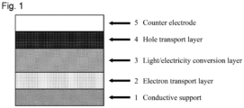
- the device of the present invention preferably includes, without limitation, the conductive support 1, the electron transport layer 2, the light/electricity conversion layer 3, the hole transport layer 4, and the counter electrode 5.
- the device of the present invention can be suitably used as a solar cell, and is more preferably, but not limited to, a perovskite device for converting light into electricity.
- the perovskite device for converting light into electricity preferably includes a conductive support (electrode) 1, an electron transport layer 2, a light/electricity conversion layer (perovskite layer) 3, a hole transport layer 4, and a counter electrode 5 in this order.
- the perovskite device may include a conductive support, a hole transport layer, a light/electricity conversion layer (perovskite layer), an electron transport layer, and a counter electrode in this order.
- the conductive support 1 shown in Fig. 1 needs to have optical transparency so as to transmit light that contributes to light/electricity conversion.
- the conductive support is a member configured to extract current from the light/electricity conversion layer, and accordingly, is preferably a conductive substrate.
- conductive materials include conductive transparent oxide semiconductors such as tin-doped indium oxide (ITO), zinc-doped indium oxide (IZO), tungsten-doped indium oxide (IWO), aluminum zinc oxide (AZO), fluorine-doped tin oxide (FTO), indium oxide (In 2 O 3 ), and indium-tin complex oxides, and it is preferable to use tin-doped indium oxide (ITO) or fluorine-doped tin oxide (FTO).
- ITO tin-doped indium oxide
- IZO zinc-doped indium oxide
- IWO tungsten-doped indium oxide
- AZO aluminum zinc oxide
- FTO fluorine-doped tin oxide
- ITO indium oxide
- FTO fluorine-doped tin oxide
- the electron transport layer 2 shown in Fig. 1 is positioned between the conductive support 1 described above and the light/electricity conversion layer (perovskite layer) 3.
- the electron transport layer 2 is preferably formed on the conductive support 1, but the position is not limited thereto.
- the electron transport layer is used to improve the efficiency in transfer of electrons from the light/electricity conversion layer to the electrode and also used to block the transfer of holes.
- Examples of a semiconductor for forming the electron transport layer include: metal oxides such as tin oxide (SnO, SnO 2 , SnO 3 , etc.), titanium oxide (TiO 2 etc.), tungsten oxide (WO 2 , WO 3 , W 2 O 3 , etc.), zinc oxide (ZnO), niobium oxides (Nb 2 O 5 etc.), tantalum oxide (Ta 2 O 5 etc.), yttrium oxide (Y 2 O 3 etc.), and strontium titanate (SrTiO 3 etc.); metal sulfides such as titanium sulfide, zinc sulfide, zirconium sulfide, copper sulfide, tin sulfide, indium sulfide, tungsten sulfide, cadmium sulfide, and silver sulfide; metal selenides such as titanium selenide, zirconium selenide, indium selenide, and tungsten
- the electron transport layer may be formed by using a commercially available paste containing microparticles of the above-described semiconductor (coating solution for an electron transport layer), or a paste or the like prepared by dispersing a commercially available semiconductor fine powder in a solvent.
- the solvent used to prepare the paste include, but are not limited to, water; alcoholic solvents such as methanol, ethanol, and isopropyl alcohol; ketone solvents such as acetone, methyl ethyl ketone, and methyl isobutyl ketone; and hydrocarbon solvents such as n-hexane, cyclohexane, benzene, and toluene. These solvents may also be used in a combination of two or more as a solvent mixture.
- the electron transport layer can be formed using a known film formation method depending on the material used.
- the method for forming the electron transport layer include, but are not limited to, a method including forming a coating film on a conductive substrate using a wet coating method, and then removing the solvent and additives therefrom through firing, and examples of the wet coating method include spin coating, inkjet coating, doctor blade coating, drop casting, squeegee coating, screen printing, reverse roll coating, gravure coating, kiss coating, roll brushing, spray coating, air knife coating, wire-bar bar coating, pipe doctor coating, impregnation and coating, and curtain coating.
- the method for forming the electron transport layer include a method including forming a film by sputtering, evaporation, electrodeposition, electrocrystallization, or microwave irradiation.
- the conditions for spin coating can be set as appropriate. There is no particular limitation on the atmosphere in which the electron transport layer is formed, and the electron transport layer may be formed in normal air.
- the film thickness of the electron transport layer is usually preferably 5 to 100 nm, and more preferably 10 to 50 nm.
- the film thickness is usually preferably 20 to 200 nm, and more preferably 50 to 150 nm.
- the light/electricity conversion layer (perovskite layer) 3 is preferably formed on the electron transport layer 2 as shown in Fig. 1 .
- examples of a perovskite material used in the light/electricity conversion layer include materials of a family having a structure represented by the general formula ABX 3 , where A, B, and X represent an organic cation or a monovalent metal cation, a metal cation, and a halide anion, respectively.
- perovskite materials represented by the compositions MAPbI 3 , FAPbI 3 , EAPbI 3 , CsPbI 3 , MASnI 3 , FASnI 3 , EASnI 3 , MAPbBr 3 , FAPbBr 3 , EAPbBr 3 , MASnBr 3 , FASnBr 3 , and EASnBr 3 , and also perovskite materials composed of mixed cations and mixed anions represented by the compositions K(FAMA)Pb(IBr) 3 , Rb(FAMA)Pb(IBr) 3 , and Cs(FAMA)Pb(IBr) 3 .
- These perovskite materials may also be used in a combination of two or more.
- the light/electricity conversion layer may contain a light absorbing agent other than a perovskite material.
- a commercially available perovskite precursor may be used, and in the present invention, a precursor obtained by mixing a lead halide, a methylammonium halide, a formamidine halide, and a cesium halide to achieve a desired composition is preferably used, but the perovskite precursor is not limited to this.
- Examples of a solvent for the perovskite precursor solution include, but are not limited to, N,N-dimethylformamide (DMF), dimethyl sulfoxide (DMSO), and ⁇ -butyrolactone, in view of the solubility of the precursor. These solvents may also be used in a combination of two or more, and a solvent mixture of N,N-dimethylformamide and dimethyl sulfoxide is preferably used.
- the atmosphere in which the light/electricity conversion layer (perovskite layer) is formed is preferably a dry atmosphere, which prevents moisture contamination to thereby enable a highly efficient device for converting light into electricity to be produced with high reproducibility, and more preferably a dry inert gas atmosphere in a glove box or the like. It is also preferable to use a solvent with low moisture content obtained by drying with a molecular sieve.
- the temperature at which the light/electricity conversion layer (perovskite layer) is heated using a hot plate or other means is preferably 50 to 200°C, and more preferably 70 to 150°C, in view of efficiently producing the perovskite material from the precursor.
- the heating time is preferably 10 to 90 minutes, and more preferably 10 to 60 minutes.
- the film thickness of the light/electricity conversion layer is preferably 50 to 1000 nm, and more preferably 300 to 700 nm, in view of more reliably suppressing degradation in performance due to a defect or delamination and also ensuring a sufficient light absorptance of the light/electricity conversion layer and not too much resistance of the device.
- the hole transport layer 4 shown in Fig. 1 is a layer that transports holes and is positioned between the light/electricity conversion layer (perovskite layer) 3 and the counter electrode 5.
- the hole transport layer is used to improve the efficiency in the transfer of holes from the light/electricity conversion layer to the electrode and also used to block the transfer of electrons.
- conductors, semiconductors, organic hole transport materials, and the like can be used, and an additive may also be contained for the purpose of further improving the hole transporting properties.
- the hole transport layer in the device of the present invention is a layer that contains the compound represented by the general formula (1) as a hole transport material.
- the hole transport layer two or more compounds represented by the general formula (1) may be used in combination.
- the compound represented by the general formula (1) may also be used in combination with another hole transport material or the like that is outside the scope of the present invention.
- organic hole transport materials examples include polythiophene derivatives such as poly-3-hexylthiophene (P3HT) and polyethylenedioxythiophene (PEDOT); fluorene derivatives such as 2,2',7,7'-tetrakis-(N,N-di-p-methoxyphenylamine)-9,9'-spirobifluorene (Spiro-OMeTAD); carbazole derivatives such as polyvinylcarbazole; triphenylamine derivatives such as poly[bis(4-phenyl) (2,4,6-trimethylphenyl)amine] (PTAA); diphenylamine derivatives; polysilane derivatives; and polyaniline derivatives.
- P3HT poly-3-hexylthiophene
- PEDOT polyethylenedioxythiophene
- fluorene derivatives such as 2,2',7,7'-tetrakis-(N,N-di-p-methoxyphenylamine)
- Examples of a solvent used in the coating solution for the hole transport layer include, but are not limited to, aromatic organic solvents such as benzene, toluene, xylene, mesitylene, tetralin (1,2,3,4-tetrahydronaphthalene), monochlorobenzene (chlorobenzene), o-dichlorobenzene, m-dichlorobenzene, p-dichlorobenzene, and nitrobenzene; alkyl halide organic solvents such as dichloromethane, chloroform, 1,2-dichloroethane, 1,1,2-trichloroethane, and dichloromethane; nitrile solvents such as benzonitrile and acetonitrile; ether solvents such as tetrahydrofuran, dioxane, diisopropyl ether, c-pentyl methyl ether, ethylene glycol dimethyl ether, ethylene glycol diethy
- the film thickness of the hole transport layer is preferably 5 to 500 nm, and more preferably 10 to 250 nm, in view of further improving the power conversion efficiency.
- the device of the present invention may contain a dopant (or an oxidizing agent) or a basic compound (or a basic additive) as an additive in the hole transport layer.
- a dopant or an oxidizing agent
- a basic compound or a basic additive
- Incorporating the additive into the hole transport layer to increase the carrier concentration of the hole transport material in the hole transport layer leads to an improvement in the conversion efficiency of the device.
- the amount of the additives is preferably 3.5 equivalents or less per 1 equivalent of the hole transport material.
- the dopant examples include lithium bis(trifluoromethylsulfonyl)imide (LiTFSI), silver bis(trifluoromethanesulfonyl)imide, tris(2-(1H-pyrazol-1-yl)-4-tert-butylpyridine)cobalt(III) tri[bis(trifluoromethane)sulfonimide] (FK209), NOSbF 6 , SbCls, and SbF 5 .
- LiTFSI lithium bis(trifluoromethylsulfonyl)imide
- the dopant used is not limited to this.
- the hole transport layer contains the basic compound
- specific examples thereof include 4-tert-butylpyridine (tBP), 2-picoline, and 2,6-lutidine.
- tBP 4-tert-butylpyridine
- 2-picoline 2-picoline
- 2,6-lutidine 2-(2-aminoethyl)-2-aminoethylpyridine
- the basic compound is often used in combination with the dopant.
- the amount of the basic compound is preferably 5 equivalents or less, and more preferably 3 equivalents or less, per 1 equivalent of the hole transport material contained in the hole transport layer.
- the counter electrode 5 shown in Fig. 1 is a layer that is disposed opposite the conductive support 1 and formed on the hole transport layer 4, and the counter electrode 5 is used to exchange charges with the hole transport layer.
- a metal electrode serving as the counter electrode is provided preferably on the hole transport layer 4.
- An electron blocking layer made of an organic material or an inorganic compound semiconductor may be interposed between the hole transport layer 4 and the counter electrode 5.
- a material used for the counter electrode include metals such as platinum, titanium, stainless steel, aluminum, gold, silver, nickel, magnesium, chromium, cobalt, and copper, and also alloys of these metals.
- gold, silver, or a silver alloy is preferably used in view of high electrical conductivity even in the form of a thin film.
- the silver alloy it is preferable to use a silver-gold alloy, a silver-copper alloy, a silver-palladium alloy, a silver-copper-palladium alloy, a silver-platinum alloy, and the like, which are less susceptible to sulfidation and chlorination and thus increase the stability of the thin film.
- the material for forming the counter electrode is preferably such that the counter electrode can be formed by using the material by evaporation or the like.
- the film thickness of the metal electrode is preferably 10 nm or greater, and more preferably 50 nm or greater, in view of obtaining favorable conductivity.
- the conductive support serves as a negative electrode, and the counter electrode serves as a positive electrode.
- the conductive support side of the device is preferably irradiated with light such as sunlight.
- the light/electricity conversion layer perovskite layer
- the light/electricity conversion layer absorbs light and becomes excited, generating electrons and holes.
- the electrons move through the electron transport layer, and the holes move through the hole transport layer, to reach the respective electrodes, thereby causing a current to flow, and thus, the device for converting light into electricity performs its function.
- the device of the present invention can be applied to perovskite solar cells, various optical sensors, and the like.
- a perovskite solar cell module the device of the present invention, which includes the hole transport material containing the compound represented by the general formula (1) as the hole transport layer, serves as a cell.
- the required number of such cells are arranged to form the solar cell module, to which predetermined electrical wiring is provided.
- the compound of the above formula (A-2) (0.60 g), malononitrile (0.20 g, manufactured by Tokyo Chemical Industry Co., Ltd.), and 25 mL of THF were placed in a reaction vessel and stirred in an argon atmosphere.
- Acetic acid 2.4 mL, manufactured by Kanto Chemical Co., Inc.
- pyridine 2.4 mL, manufactured by Nacalai Tesque, Inc.
- the reaction solution was put into a beaker containing 300 mL of water.
- the resulting mixture was filtered, and the residue on the filter was washed with 30 mL of water and with 20 mL of methanol.
- the compound of the above formula (A-2) (0.6 g), diethyl malonate (0.37 g, manufactured by Tokyo Chemical Industry Co., Ltd.), and THF (14 mL) were placed in a reaction vessel and stirred in an argon atmosphere. The mixture was cooled to 5°C or below in an ice bath, and pyridine (1 mL) was added. The mixture was cooled again to 5°C or below, and titanium tetrachloride (0.5 mL, manufactured by Wako Pure Chemical Industries, Ltd.) was added. The temperature was then raised to room temperature, and the mixture was stirred at room temperature for 17 hours.
- the compound of the above formula (A-2) (0.65 g), methyl cyanoacetate (0.33 g, manufactured by Tokyo Chemical Industry Co., Ltd.), and THF (25 mL) were placed in a reaction vessel and stirred in an argon atmosphere.
- the mixture was cooled to 5°C or below in an ice bath, and pyridine (1 mL) was added.
- the mixture was cooled again to 5°C or below, and titanium tetrachloride (0.55 mL, manufactured by Wako Pure Chemical Industries, Ltd.) was added.
- the temperature was then raised to room temperature, and the mixture was stirred at room temperature for 8 hours, and then stirred for 2 hours while heating under reflux.
- 2,7-dibromofluorenone (0.47 g), the compound of the formula (11) below (2.57 g), tetrakis(triphenylphosphine)palladium(0) (0.065 g, manufactured by Kanto Chemical Co., Inc.), potassium carbonate (0.51 g, manufactured by Kanto Chemical Co., Inc.), toluene (7.5 mL), ethanol (2.5 mL), and water (2.5 mL) were placed in a reaction vessel and degassed under reduced pressure. The mixture was heated under reflux for 7 hours in an argon atmosphere. After the reaction was completed, toluene (20 mL) and water (10 mL) were added. The resulting mixture was subjected to liquid-liquid separation.
- 2,7-dibromofluorenone (0.68 g, manufactured by Tokyo Chemical Industry Co., Ltd.), the compound of the formula (12) below (2.52 g), potassium carbonate (0.72 g, manufactured by Kanto Chemical Co., Inc.), tetrakis(triphenylphosphine)palladium (0.09 g, manufactured by Kanto Chemical Co., Inc.), toluene (11 mL), ethanol (3 mL), and water (3 mL) were placed in a reaction vessel and degassed under reduced pressure. The mixture was stirred for 10 hours while heating under reflux. After the reaction was completed, the reaction solution was put into a beaker containing water (100 mL).
- reaction solution was cooled to 40°C or below, and water (10 mL) and methanol (10 mL) were added.
- the resulting mixture was filtered, and the residue on the filter was washed with methanol (10 mL) and dried.
- the compound of the above formula (13) (0.50 g), the compound of the above formula (9) (1.89 g), potassium carbonate (0.37 g, manufactured by Kanto Chemical Co., Inc.), tetrakis triphenylphosphinepalladium (0.05 g, manufactured by Kanto Chemical Co., Inc.), toluene (10 mL), ethanol (2.3 mL), and water (2.3 mL) were placed in a reaction vessel and degassed under reduced pressure. The mixture was heated under reflux for 13 hours. After the reaction was completed, the reaction solution was put into a beaker containing water (100 mL).
- the resulting mixture was filtered, and the residue on the filter was washed with water (10 mL) and with methanol (30 mL), and dried.
- a glass substrate with an etched, fluorine-doped tin oxide (FTO) coating (conductive support 1, manufactured by Solaronix) was ultrasonically cleaned in isopropyl alcohol and then treated with UV/ozone.
- FTO fluorine-doped tin oxide
- the perovskite precursor solution was dropped on the tin oxide thin film, followed by spin-coating. During the spin-coating, 0.3 mL of chlorobenzene was dropped. Thus, a perovskite precursor film was formed.
- the resultant was heated at 100°C for 1 hour using a hot plate, to thereby form a Cs(MAFA)Pb(IBr) 3 layer (light/electricity conversion layer 3) having a film thickness of about 500 nm.
- the Cs(MAFA)Pb(IBr) 3 layer (light/electricity conversion layer 3) was spin-coated with the coating solution for a hole transport layer, to thereby form a hole transport layer 4 having a film thickness of about 200 nm.
- Vacuum evaporation was performed (degree of vacuum: about 1 ⁇ 10 -4 Pa) to form a gold film having a thickness of 80 to 100 nm as a gold electrode (counter electrode 5) on the hole transport layer.
- the conductive support side of the device for converting light into electricity was irradiated with simulated sunlight (AM1.5, 100 mW/cm 2 ) generated by a solar simulator (model OTENTO-SUN SH, manufactured by Bunkoukeiki Co., Ltd.), and power conversion efficiency was determined by determining current-voltage characteristics using a source meter (Model 2400 Series SourceMeter, manufactured by KEITHLEY). Table 1 shows the current-voltage characteristics and the power conversion efficiency.
- a device for converting light into electricity was produced in the same manner as in Example 1, except that, instead of the compound (A-2), the compound (A-15) was dissolved in the dopant solution in chlorobenzene to a concentration of 30 mM and used. Then, the power conversion efficiency was determined by determining current-voltage characteristics in the same manner as in Example 1. Table 1 shows the current-voltage characteristics and the power conversion efficiency.
- a device for converting light into electricity was produced in the same manner as in Example 1, except that the compound (A-28) was used instead of the compound (A-2). Then, the power conversion efficiency was determined by determining current-voltage characteristics in the same manner as in Example 1. Table 1 shows the current-voltage characteristics and the power conversion efficiency.
- a device for converting light into electricity was produced in the same manner as in Example 1, except that the compound (A-41) was used instead of the compound (A-2). Then, the power conversion efficiency was determined by determining current-voltage characteristics in the same manner as in Example 1. Table 1 shows the current-voltage characteristics and the power conversion efficiency.
- Example 1 A device for converting light into electricity was produced in the same manner as in Example 1, except that the compound (A-67) was used instead of the compound (A-2). Then, the power conversion efficiency was determined by determining current-voltage characteristics in the same manner as in Example 1. Table 1 shows the current-voltage characteristics and the power conversion efficiency.
- a device for converting light into electricity was produced in the same manner as in Example 1, except that a standard hole transport material Spiro-OMeTAD (manufactured by Sigma-Aldrich) represented by the formula (B-1) below was used instead of the compound (A-2). Then, the power conversion efficiency was determined by determining current-voltage characteristics in the same manner as in Example 1. Table 1 shows the current-voltage characteristics and the power conversion efficiency.
- Table 1 Hole transport material Short-circuit current density Jsc [mA/cm 2 ] Open-circuit voltage Voc [V] Fill factor FF Power conversion efficiency PCE [%] Ex. 1 (A-2) 22.28 1.07 0.72 17.43 Ex. 2 (A-15) 22.61 1.04 0.66 15.81 Ex.
- the devices for converting light into electricity each including, as the hole transport material, the compound (A-2), (A-15), (A-28), (A-41), or (A-67) having the fluorenone skeleton, which is a compound of the present invention, exhibited higher efficiencies in conversion of light into electricity than the device including the compound (B-1), which is a standard hole transport material.
- Tin(IV) oxide 15% in H 2 O colloidal dispersion (manufactured by Alfa Aesar) and purified water were mixed in a volume ratio of 1:9 to obtain a tin oxide dispersion (coating solution for an electron transport layer), and the ITO coating was spin coated with the coating solution for an electron transport layer. After that, the resultant was heated at 150°C for 30 minutes using a hot plate to form a tin oxide thin film (electron transport layer 2) having a thickness of about 20 nm.
- the conductive support side of the device for converting light into electricity was irradiated with simulated sunlight (AM1.5, 100 mW/cm 2 ) generated by a solar simulator (model OTENTO-SUN SH, manufactured by Bunkoukeiki Co., Ltd.), and the initial power conversion efficiency was determined by determining current-voltage characteristics using a source meter (Model 2400 Series SourceMeter, manufactured by KEITHLEY). Table 2 shows the current-voltage characteristics and the initial power conversion efficiency.
- the device for converting light into electricity was stored in a desiccator containing silica gel for 30 days. Then, current-voltage characteristics were determined again under simulated sunlight irradiation to determine the power conversion efficiency after 30 days.
- a device for converting light into electricity was produced in the same manner as in Example 6, except that, instead of the compound (A-36), the compound (A-96) was dissolved in the dopant solution in chlorobenzene to a concentration of 40 mM at room temperature and used. Then, the initial power conversion efficiency and the power conversion efficiency after 30 days were determined in the same manner as in Example 6. Table 2 shows the initial power conversion efficiency. The retention (%) was calculated using the above formula (a-1) from the power conversion efficiency after 30 days. Table 2 also shows the retention.
- a device for converting light into electricity was produced in the same manner as in Example 6, except that, instead of the compound (A-36), the compound (A-83) was dissolved in the dopant solution in chlorobenzene to a concentration of 50 mM at room temperature and used. Then, the initial power conversion efficiency and the power conversion efficiency after 30 days were determined in the same manner as in Example 6. Table 2 shows the initial power conversion efficiency. The retention (%) was calculated using the above formula (a-1) from the power conversion efficiency after 30 days. Table 2 also shows the retention.
Landscapes
- Chemical & Material Sciences (AREA)
- Organic Chemistry (AREA)
- Engineering & Computer Science (AREA)
- Materials Engineering (AREA)
- Physics & Mathematics (AREA)
- Spectroscopy & Molecular Physics (AREA)
- Electromagnetism (AREA)
- Inorganic Chemistry (AREA)
- Photovoltaic Devices (AREA)
- Electroluminescent Light Sources (AREA)
- Heterocyclic Carbon Compounds Containing A Hetero Ring Having Nitrogen And Oxygen As The Only Ring Hetero Atoms (AREA)
Abstract

Description
- The present invention relates to a compound, a hole transport material, and a device for converting light into electricity, the device including the hole transport material.
- In recent years, photovoltaic power generation has been gaining attention as a clean energy source, and solar cells has been actively developed. In particular, the development of solar cells having a perovskite material-containing layer to convert light into electricity (hereinafter referred to as "perovskite solar cells") is gaining attention (see
Patent Literature 1 and Non-PatentLiteratures - A hole transport material is often used in perovskite solar cells. The purposes of using the hole transport material include: (1) enhancing the ability to selectively transport holes to thereby improve the efficiency in conversion of light into electricity (i.e., power conversion efficiency), and (2) joining the hole transport material to the perovskite layer, which is for converting light into electricity, to thereby protect a perovskite material, which is susceptible to moisture and oxygen (see Non-Patent
Literature 3, for example) (hereinafter, converting (or conversion of) light into electricity is also referred to as "light/electricity conversion"). A spirobifluorene-based organic compound Spiro-OMeTAD is often used as a standard hole transport material, and there have been few reports on a hole transport material that contributes more to light/electricity conversion characteristics than Spiro-OMeTAD. - Patent Literature 1:
US 10937972B2 -
- Non-Patent Literature 1: Journal of the American Chemical Society, 2009, Vol. 131, pp. 6050-6051
- Non-Patent Literature 2: Science, 2012, Vol. 388, pp. 643-647
- Non-Patent Literature 3: Chem. Sci., 2019, 10, pp. 6748-6769
- It is an object of the present invention to provide a compound that is useful as a hole transport material for providing a device for converting light into electricity that is capable of extracting current with high efficiency, and a device for converting light into electricity and a solar cell that include the compound in a hole transport layer and have favorable light/electricity conversion characteristics.
- To achieve the above-described object, the inventors of the present invention have conducted in-depth research on improving light/electricity conversion characteristics and have found that a device for converting light into electricity and a perovskite solar cell that exhibit high efficiency in conversion of light into electricity can be obtained by designing and developing a compound with a specific structure and using this compound as a hole transport layer in the device for converting light into electricity. Specifically, the present invention is summarized as follows.
- 1. A compound represented by the general formula (1) below.

- In this formula, R1 to R20 each independently represent a hydrogen atom, a halogen atom, a carboxyl group, a trimethylsilyl group, a linear or branched alkyl group having 1 to 20 carbon atoms and optionally having a substituent, a linear or branched alkenyl group having 2 to 20 carbon atoms and optionally having a substituent, a cycloalkyl group having 3 to 10 carbon atoms and optionally having a substituent, an alkyloxy group having 1 to 20 carbon atoms and optionally having a substituent, a cycloalkyloxy group having 3 to 10 carbon atoms and optionally having a substituent, an acyl group having 1 to 20 carbon atoms and optionally having a substituent, a thio group having 1 to 18 carbon atoms and optionally having a substituent, an amino group having 1 to 20 carbon atoms and optionally having a substituent, an aromatic hydrocarbon group having 6 to 36 carbon atoms and having a substituent, or a heterocyclic group having 5 to 36 ring-forming atoms and optionally having a substituent;
- R1 and R2; R2 and R3; R3 and R4; R4 and R5; R6 and R7; R7 and R8; R8 and R9; R9 and R10; R11 and R12; R12 and R13; R13 and R14; R14 and R15; R16 and R17; R17 and R18; R18 and R19; and R19 and R20 are, in each combination, optionally bonded to each other to form a ring; and R5 and R6; and R15 and R16 are, in each combination, optionally bonded to each other to form a ring;
- X1 and X2 each represent a divalent group; and
- Y represents an oxygen atom or CR21R22,
- where R21 and R22 each independently represent a nitrile group, an acyl group having 1 to 10 carbon atoms and optionally having a substituent, or an alkoxycarbonyl group having 1 to 10 carbon atoms and optionally having a substituent, and R21 and R22 are optionally bonded to each other to form a ring.
- 2. The above-described compound, wherein, in the general formula (1), X1 and X2 are represented by the general formula (2) below.

- In this formula, R23 to R28 each independently represent a hydrogen atom, a linear or branched alkyl group having 1 to 10 carbon atoms and optionally having a substituent, a linear or branched alkenyl group having 2 to 10 carbon atoms and optionally having a substituent, a cycloalkyl group having 3 to 10 carbon atoms and optionally having a substituent, an aromatic hydrocarbon group having 6 to 18 carbon atoms and optionally having a substituent, or a heterocyclic group having 5 to 18 ring-forming atoms and optionally having a substituent;
- R23 and R24; R25 and R26; and R27 and R28 are, in each combination, optionally bonded to each other to form a ring;
- Z represents an oxygen atom, a sulfur atom, or a selenium atom; and
- m and n represent integers of 0 to 2, with the proviso that cases where both m and n are 0 are excluded.
- 3. The above-described compound, wherein, in the general formula (2), m is 1.
- 4. The above-described compound, wherein, in the general formula (1), R1 to R20 are each independently a hydrogen atom, a linear or branched alkyl group having 1 to 20 carbon atoms and optionally having a substituent, an alkoxy group having 1 to 20 carbon atoms and optionally having a substituent, a thio group having 1 to 18 carbon atoms and optionally having a substituent, or an amino group having 1 to 20 carbon atoms and optionally having a substituent.
- 5. A hole transport material including the above-described compound.
- 6. A device for converting light into electricity, including the above-described hole transport material.
- The compound and the hole transport layer including the compound according to the present invention enable a device for converting light into electricity and a perovskite solar cell that have favorable power conversion efficiency.
- [
Fig. 1] Fig. 1 is a schematic cross-sectional view showing the configuration of the devices for converting light into electricity of Examples and Comparative Examples. - Embodiments of the present invention will be described in detail below. The hole transport material of the present invention is suitably used for a device for converting light into electricity and a perovskite solar cell.
- As shown in the schematic cross-sectional view of
Fig. 1 , a device for converting light into electricity of the present invention (hereinafter, also simply referred to as "the device of the present invention) typically has aconductive support 1; anelectron transport layer 2; a layer that convers light into electricity (hereinafter also referred to as "light/electricity conversion layer"), 3; ahole transport layer 4; and acounter electrode 5. - Hereinafter, a compound represented by the general formula (1) above, which serves as a hole transport material for use in the hole transport layer of the device of the present invention, will be described specifically, but the present invention is not limited to the following descriptions.
- R1 to R20 in the general formula (1) each independently represent a hydrogen atom, a halogen atom, a carboxyl group, a trimethylsilyl group, a linear or branched alkyl group having 1 to 20 carbon atoms and optionally having a substituent, a linear or branched alkenyl group having 2 to 20 carbon atoms and optionally having a substituent, a cycloalkyl group having 3 to 10 carbon atoms and optionally having a substituent, an alkyloxy group having 1 to 20 carbon atoms and optionally having a substituent, a cycloalkyloxy group having 3 to 10 carbon atoms and optionally having a substituent, an acyl group having 1 to 20 carbon atoms and optionally having a substituent, a thio group having 1 to 18 carbon atoms and optionally having a substituent, an amino group having 1 to 20 carbon atoms and optionally having a substituent, an aromatic hydrocarbon group having 6 to 36 carbon atoms and having a substituent, or a heterocyclic group having 5 to 36 ring-forming atoms and optionally having a substituent.
- Examples of the "halogen atom" represented by R1 to R20 include fluorine, chlorine, bromine, and iodine.
- Examples of the "linear or branched alkyl group having 1 to 20 carbon atoms" of the "linear or branched alkyl group having 1 to 20 carbon atoms and optionally having a substituent" represented by R1 to R20 include: a methyl group, an ethyl group, an n-propyl group, an isopropyl group, an n-butyl group, an isobutyl group, an s-butyl group, a t-butyl group, an n-pentyl group, an isopentyl group, an n-hexyl group, a 2-ethylhexyl group, a heptyl group, an octyl group, an isooctyl group, a nonyl group, and a decyl group.
- Examples of the "linear or branched alkenyl group having 2 to 20 carbon atoms" of the "linear or branched alkenyl group having 2 to 20 carbon atoms and optionally having a substituent" represented by R1 to R20 include: an ethenyl group (vinyl group), a 1-propenyl group, a 2-propenyl group (allyl group), a 1-methylethenyl group, a 1-butenyl group, a 2-butenyl group, a 1-pentenyl group, a 1-hexenyl group, a 2-methyl-1-propenyl group, a 2-methyl-2-propenyl group, and a 1-ethylethenyl group, and also a linear or branched alkenyl group having 2 to 20 carbon atoms that is composed of a plurality of these alkenyl groups linked together.
- Examples of the "cycloalkyl group having 3 to 10 carbon atoms" of the "cycloalkyl group having 3 to 10 carbon atoms and optionally having a substituent" represented by R1 to R20 include: a cyclopropyl group, a cyclobutyl group, a cyclopentyl group, a cyclohexyl group, a cycloheptyl group, a cyclooctyl group, a cyclodecyl group, a cyclododecyl group, a 4-methylcyclohexyl group, and a 4-ethylcyclohexyl group.
- Examples of the "alkoxy group having 1 to 20 carbon atoms" of the "alkoxy group having 1 to 20 carbon atoms and optionally having a substituent" represented by R1 to R20 include: a methoxy group, an ethoxy group, a propoxy group, an n-butoxy group, an n-pentyloxy group, an n-hexyloxy group, a heptyloxy group, an octyloxy group, a nonyloxy group, a decyloxy group, an isopropoxy group, an isobutoxy group, an s-butoxy group, a t-butoxy group, an isooctyloxy group, a t-octyloxy group, a phenoxy group, a tolyloxy group, a biphenylyloxy group, a terphenylyloxy group, a naphthyloxy group, an anthryloxy group, a phenanthryloxy group, a fluorenyloxy group, and an indenyloxy group.
- Examples of the "cycloalkyloxy group having 3 to 10 carbon atoms" of the "linear or branched cycloalkyloxy group having 3 to 10 carbon atoms and optionally having a substituent" represented by R1 to R20 include: a cyclopropoxy group, a cyclobutoxy group, a cyclopentyloxy group, a cyclohexyloxy group, and a 4-methylcyclohexyloxy group.
- Examples of the "acyl group having 1 to 20 carbon atoms" of the "acyl group having 1 to 20 carbon atoms and optionally having a substituent" represented by R1 to R20 include: an acetyl group, a propionyl group, a butyryl group, an isobutyryl group, a valeryl group, an isovaleryl group, a benzoylacetyl group, and a benzoyl group. One or more hydrogen atoms of the alkyl group in the acyl group may be replaced with fluorine atoms, and all of the hydrogen atoms may be replaced with fluorine atoms (that is, perfluorinated). The acyl group may be bonded to an amino group (-CO-N<).
- Examples of the "thio group having 1 to 18 carbon atoms" of the "thio group having 1 to 18 carbon atoms and optionally having a substituent" represented by R1 to R20 include: a methylthio group, an ethylthio group, a propylthio group, a phenylthio group, and a biphenylthio group.
- Examples of the "amino group having 1 to 20 carbon atoms" of the "amino group having 1 to 20 carbon atoms and optionally having a substituent" represented by R1 to R20 include: mono-substituted amino groups such as an ethylamino group, an acetylamino group, and a phenylamino group; and di-substituted amino groups such as a diethylamino group, a diphenylamino group, and an acetylphenylamino group.
- Examples of the "aromatic hydrocarbon group having 6 to 36 carbon atoms" of the "aromatic hydrocarbon group having 6 to 36 carbon atoms and optionally having a substituent" represented by R1 to R20 include: a phenyl group, a biphenyl group, a terphenyl group, a naphthyl group, a biphenyl group, an anthracenyl group (anthryl group), a phenanthryl group, a fluorenyl group, an indenyl group, a pyrenyl group, a perylenyl group, a fluoranthenyl group, and a triphenylenyl group. In the present invention, the aromatic hydrocarbon group encompasses a "fused polycyclic aromatic group".
- Examples of the "heterocyclic group having 5 to 36 ring-forming atoms" of the "heterocyclic group having 5 to 36 ring-forming atoms and optionally having a substituent" represented by R1 to R20 include: a pyridyl group, a pyrimidinyl group, a triazinyl group, a thienyl group, a furyl group (furanyl group), a pyrrolyl group, an imidazolyl group, a pyrazolyl group, a triazolyl group, a quinolyl group, an isoquinolyl group, a naphthyldinyl group, an acridinyl group, a phenanthrolinyl group, a benzofuranyl group, a benzothienyl group, an oxazolyl group, an indolyl group, a carbazolyl group, a benzoxazolyl group, a thiazolyl group, a benzothiazolyl group, a quinoxalinyl group, a benzimidazolyl group, a pyrazolyl group, a dibenzofuranyl group, a dibenzothienyl group, and a carbonylyl group.
- Examples of the "substituent" of the "linear or branched alkyl group having 1 to 18 carbon atoms and optionally having a substituent", the "linear or branched alkenyl group having 2 to 20 carbon atoms and optionally having a substituent", the "cycloalkyl group having 3 to 10 carbon atoms and optionally having a substituent", the "alkyloxy group having 1 to 20 carbon atoms and optionally having a substituent", the "cycloalkyloxy group having 3 to 10 carbon atoms and optionally having a substituent", the "acyl group having 1 to 20 carbon atoms and optionally having a substituent", the "thio group having 1 to 18 carbon atoms and optionally having a substituent", the "amino group having 1 to 20 carbon atoms and optionally having a substituent", the "aromatic hydrocarbon group having 6 to 36 carbon atoms and having a substituent", or the "heterocyclic group having 5 to 36 ring-forming atoms and optionally having a substituent" include: halogen atoms such as a fluorine atom, a chlorine atom, a bromine atom, and an iodine atom; a cyano group; a hydroxyl group; a nitro group; a nitroso group; a carboxyl group; a phosphate group: a thioxo group (>C=S); a trimethylsilyl group; carboxylic acid ester groups such as methyl ester groups and ethyl ester groups; linear or branched alkyl groups having 1 to 18 carbon atoms such as a methyl group, an ethyl group, an n-propyl group, an isopropyl group, an n-butyl group, an isobutyl group, an s-butyl group, a t-butyl group, an n-pentyl group, an isopentyl group, an n-hexyl group, a 2-ethylhexyl group, a heptyl group, an octyl group, an isooctyl group, a nonyl group, and a decyl group; linear or branched alkenyl groups having 2 to 18 carbon atoms such as an ethenyl group (vinyl group), a 1-propenyl group, a 2-propenyl group (allyl group), a 1-butenyl group, a 2-butenyl group, a 1-pentenyl group, a 1-hexenyl group, a 2-methyl-1-propenyl group, a 2-methyl-2-propenyl group, and a 1-ethylethenyl group; alkoxy groups having 1 to 18 carbon atoms such as a methoxy group, an ethoxy group, a propoxy group, a t-butoxy group, a pentyloxy group, and a hexyloxy group; aromatic hydrocarbon groups having 6 to 30 carbon atoms such as a phenyl group, a naphthyl group, an anthryl group, a phenanthryl group, and a pyrenyl group; heterocyclic groups having 5 to 30 ring-forming atoms such as a pyridyl group, a pyrimidinyl group, a triazinyl group, a thienyl group, a furyl group (furanyl group), a pyrrolyl group, an imidazolyl group, a pyrazolyl group, a triazolyl group, a quinolyl group, an isoquinolyl group, a naphthyldinyl group, an acridinyl group, a phenanthrolinyl group, a benzofuranyl group, a benzothienyl groups, an oxazolyl group, an indolyl group, a carbazolyl group, a benzooxazolyl group, a thiazolyl group, a benzothiazolyl group, a quinoxalinyl group, a benzimidazolyl group, a pyrazolyl group, a dibenzofuranyl group, a dibenzothienyl group, and a carbonylyl group; amino groups having 0 to 18 carbon atoms such as an unsubstituted amino group (-NH2), mono-substituted amino groups such as an ethylamino group, an acetylamino group, and a phenylamino group, and di-substituted amino groups such as a diethylamino group, a diphenylamino group, and an acetylphenylamino group; and thio groups having 0 to 18 carbon atoms such as an unsubstituted thio group (thiol group: -SH), a methylthio group, an ethylthio group, a propylthio group, a phenylthio group, and a biphenylthio groups. A plurality of "substituents" as described above may be contained, and when a plurality of substituents are contained, the substituents may be the same or different. These "substituents" may further have any of the substituents as listed above.
- In the present invention, R1 to R20 are, each independently, preferably a hydrogen atom, a linear or branched alkyl group having 1 to 20 carbon atoms and optionally having a substituent, an alkoxy group having 1 to 20 carbon atoms and optionally having a substituent, a thio group having 1 to 18 carbon atoms and optionally having a substituent, or an amino group having 1 to 20 carbon atoms and optionally having a substituent, and more preferably a hydrogen atom or an alkoxy group having 1 to 10 carbon atoms. In particular, it is preferable that R1, R2, R4, R5, R6, R7, R9, R10, R11, R12, R14, R15, R16, R17, R19, and R20 are hydrogen atoms, and at the same time, that R3, R8, R13, and R18 are alkoxy groups having 1 to 10 carbon atoms, in view of favorable power conversion efficiency when used as a hole transport material in a device for converting light into electricity.
- In the present invention, R1 and R2; R2 and R3; R3 and R4; R4 and R5; R6 and R7; R7 and R8; R8 and R9; R9 and R10; R11 and R12; R12 and R13; R13 and R14; R14 and R15; R16 and R17; R17 and R18; R18 and R19; and R19 and R20 may be, in each combination, bonded to each other to form a ring via a single bond, an oxygen atom, a sulfur atom, a selenium atom, or a nitrogen atom. R5 and R6; and R15 and R16 may also be, in each combination, bonded to each other to form a ring via a single bond, an oxygen atom, a sulfur atom, a selenium atom, or a nitrogen atom. When R5 and R6, and/or R15 and R16 form rings, the members in each combination are preferably bonded to each other to form a ring via a single bond, an oxygen atom, or a sulfur atom, and more preferably bonded to each other to form a ring via a single bond.
- In the present invention, Y represents an oxygen atom or CR21R22, where R21 and R22 each independently represent a nitrile group, an acyl group having 1 to 10 carbon atoms and optionally having a substituent, or an alkoxycarbonyl group having 1 to 10 carbon atoms and optionally having a substituent, and are preferably electron-withdrawing groups.
- Examples of the "acyl group having 1 to 10 carbon atoms and optionally having a substituent" represented by R21 and R22 include those having 1 to 10 carbon atoms, among the above-listed examples of the "acyl group having 1 to 20 carbon atoms and optionally having a substituent" represented by R1 to R20.
- Examples of the "alkoxycarbonyl group having 1 to 10 carbon atoms" of the "alkoxycarbonyl group having 1 to 10 carbon atoms and optionally having a substituent" represented by R21 and R22 include a methoxycarbonyl group and an ethoxycarbonyl group. One or more hydrogen atoms of the alkyl group in the alkoxycarbonyl group may be replaced with fluorine atoms, and all of the hydrogen atoms may be replaced with fluorine atoms (that is, perfluorinated).
- R21 and R22 may be bonded to each other to form a ring via a single bond, an oxygen atom, a sulfur atom, a selenium atom, or a nitrogen atom. When R21 and R22 from a ring, the ring is preferably an acidic heterocyclic ring such as a barbituric acid ring, a thiobarbituric acid ring, or an indanedione ring.
- In the present invention, it is preferable that X1 and X2 in the general formula (1) each should be a divalent group represented by the general formula (2) above, in view of favorable power conversion efficiency when the compound is used as a hole transport material in a device for converting light into electricity.
- R23 to R28 in the general formula (2) each independently represent a hydrogen atom, a linear or branched alkyl group having 1 to 10 carbon atoms and optionally having a substituent, a linear or branched alkenyl group having 2 to 10 carbon atoms and optionally having a substituent, a cycloalkyl group having 3 to 10 carbon atoms and optionally having a substituent, an aromatic hydrocarbon group having 6 to 18 carbon atoms and optionally having a substituent, or a heterocyclic group having 5 to 18 ring-forming atoms and optionally having a substituent.
- Examples of the "linear or branched alkyl group having 1 to 10 carbon atoms and optionally having a substituent" represented by R23 to R28 include those having 1 to 10 carbon atoms, among the above-listed examples of the "linear or branched alkyl group having 1 to 20 carbon atoms and optionally having a substituent" represented by R1 to R20.
- Examples of the "linear or branched alkenyl group having 2 to 10 carbon atoms and optionally having a substituent" represented by R23 to R28 include those having 2 to 10 carbon atoms, among the above-listed examples of the "linear or branched alkenyl group having 2 to 20 carbon atoms and optionally having a substituent" represented by R1 to R20.
- Examples of the "cycloalkyl group having 3 to 10 carbon atoms and optionally having a substituent" represented by R23 to R28 include those listed above as examples of the "cycloalkyl group having 3 to 10 carbon atoms and optionally having a substituent" represented by R1 to R20.
- Examples of the "aromatic hydrocarbon group having 6 to 18 carbon atoms and optionally having a substituent" represented by R23 to R28 include those having 6 to 18 carbon atoms, among the above-listed examples of the "aromatic hydrocarbon group having 6 to 36 carbon atoms and optionally having a substituent" represented by R1 to R20.
- Examples of the "heterocyclic group having 5 to 18 ring-forming atoms and optionally having a substituent" represented by R23 to R28 include those having 5 to 18 ring-forming atoms, among the above-listed examples of the "heterocyclic group having 5 to 36 ring-forming atoms and optionally having a substituent" represented by R1 to R20.
- R23 and R24; R25 and R26; and R27 and R28 may be, in each combination, bonded to each other to form a ring via a single bond, an oxygen atom, a sulfur atom, a selenium atom, or a nitrogen atom.
- Z in the general formula (2) represents an oxygen atom, a sulfur atom, or a selenium atom.
- In the present invention, Z is preferably a sulfur atom.
- m and n in the general formula (2) represent integers of 0 to 2; with the proviso that, when m is 0, n is 1 or 2, and when n is 0, m is 1 or 2. In other words, cases where both m and n are 0 are excluded. m is preferably 1. n is preferably 0 or 1. The group represented by the general formula (2) may be bonded, at its moiety of the phenyl group or at its moiety of the five-membered heterocyclic group, to the fluorenone moiety serving as the central skeleton of the general formula (1).
- Specific examples of the compound represented by the general formula (1) of the present invention are given below, but the present invention is not limited to these examples. The compounds illustrated below are shown with a plurality of hydrogen atoms, carbon atoms, and others omitted. The compounds illustrated below each merely represent an exemplar among possible isomers and should be construed to encompass all of the other isomers. The compounds each may be a mixture of two or more isomers.


- The compound represented by the general formula (1) can be synthesized using a known method.
- For example, the compound can be synthesized by performing a Suzuki-Miyaura cross-coupling reaction between 2,7-dibromofluorenone represented by the formula (3) below and boronic acid compounds represented by the general formulae (4) and (5) below or boronate ester compounds represented by the general formulae (6) and (7) below and subjecting the reaction product to a Knoevenagel condensation reaction with a compound represented by the general formula (8) below.


- The symbols in the formulae are as defined in the general formula (1).

- The symbols in the formulae are as defined in the general formula (1).


- The symbols in the formulae are as defined in the general formula (1).
- The compound represented by the general formula (1) may be purified by, for example, column chromatography; adsorption with silica gel, activated carbon, activated clay, or the like; or recrystallization or crystallization from a solvent. It is also effective to use a compound with higher purity obtained by performing these methods in combination. The compound can be identified through nuclear magnetic resonance (NMR) spectroscopy.
- Hereinafter, a preferred mode of the device for converting light into electricity of the present invention will be described.
- As shown in
Fig. 1 , the device of the present invention preferably includes, without limitation, theconductive support 1, theelectron transport layer 2, the light/electricity conversion layer 3, thehole transport layer 4, and thecounter electrode 5. Also, the device of the present invention can be suitably used as a solar cell, and is more preferably, but not limited to, a perovskite device for converting light into electricity. In the present invention, the perovskite device for converting light into electricity preferably includes a conductive support (electrode) 1, anelectron transport layer 2, a light/electricity conversion layer (perovskite layer) 3, ahole transport layer 4, and acounter electrode 5 in this order. Alternatively, the perovskite device may include a conductive support, a hole transport layer, a light/electricity conversion layer (perovskite layer), an electron transport layer, and a counter electrode in this order. - In the device of the present invention, the
conductive support 1 shown inFig. 1 needs to have optical transparency so as to transmit light that contributes to light/electricity conversion. In addition, the conductive support is a member configured to extract current from the light/electricity conversion layer, and accordingly, is preferably a conductive substrate. Specific examples of conductive materials include conductive transparent oxide semiconductors such as tin-doped indium oxide (ITO), zinc-doped indium oxide (IZO), tungsten-doped indium oxide (IWO), aluminum zinc oxide (AZO), fluorine-doped tin oxide (FTO), indium oxide (In2O3), and indium-tin complex oxides, and it is preferable to use tin-doped indium oxide (ITO) or fluorine-doped tin oxide (FTO). - In the device of the present invention, the
electron transport layer 2 shown inFig. 1 is positioned between theconductive support 1 described above and the light/electricity conversion layer (perovskite layer) 3. Theelectron transport layer 2 is preferably formed on theconductive support 1, but the position is not limited thereto. The electron transport layer is used to improve the efficiency in transfer of electrons from the light/electricity conversion layer to the electrode and also used to block the transfer of holes. - Examples of a semiconductor for forming the electron transport layer include: metal oxides such as tin oxide (SnO, SnO2, SnO3, etc.), titanium oxide (TiO2 etc.), tungsten oxide (WO2, WO3, W2O3, etc.), zinc oxide (ZnO), niobium oxides (Nb2O5 etc.), tantalum oxide (Ta2O5 etc.), yttrium oxide (Y2O3 etc.), and strontium titanate (SrTiO3 etc.); metal sulfides such as titanium sulfide, zinc sulfide, zirconium sulfide, copper sulfide, tin sulfide, indium sulfide, tungsten sulfide, cadmium sulfide, and silver sulfide; metal selenides such as titanium selenide, zirconium selenide, indium selenide, and tungsten selenide; and elemental semiconductors such as silicon and germanium. These semiconductors may also be used in combinations of two or more. In the present invention, it is preferable to use one or more selected from tin oxide, titanium oxide, and zinc oxide as the semiconductor.
- The electron transport layer may be formed by using a commercially available paste containing microparticles of the above-described semiconductor (coating solution for an electron transport layer), or a paste or the like prepared by dispersing a commercially available semiconductor fine powder in a solvent. Specific examples of the solvent used to prepare the paste include, but are not limited to, water; alcoholic solvents such as methanol, ethanol, and isopropyl alcohol; ketone solvents such as acetone, methyl ethyl ketone, and methyl isobutyl ketone; and hydrocarbon solvents such as n-hexane, cyclohexane, benzene, and toluene. These solvents may also be used in a combination of two or more as a solvent mixture.
- For dispersing the semiconductor fine powder in the solvent, a disperser may be used, including a ball mill, a paint conditioner, a vertical bead mill, a horizontal bead mill, and an attritor, and the powder may be ground in a mortar or the like before use. In preparing a paste, a surfactant or the like is preferably added to prevent aggregation of semiconductor fine particles, and a thickening agent such as polyethylene glycol is preferably added to impart viscosity.
- The electron transport layer can be formed using a known film formation method depending on the material used. Examples of the method for forming the electron transport layer include, but are not limited to, a method including forming a coating film on a conductive substrate using a wet coating method, and then removing the solvent and additives therefrom through firing, and examples of the wet coating method include spin coating, inkjet coating, doctor blade coating, drop casting, squeegee coating, screen printing, reverse roll coating, gravure coating, kiss coating, roll brushing, spray coating, air knife coating, wire-bar bar coating, pipe doctor coating, impregnation and coating, and curtain coating. Other examples of the method for forming the electron transport layer include a method including forming a film by sputtering, evaporation, electrodeposition, electrocrystallization, or microwave irradiation. In the present invention, it is preferable to form the electron transport layer by spin coating using a coating solution for the electron transport layer that has been prepared in the above-described manner, but the method for forming the electron transport layer is not limited to this. The conditions for spin coating can be set as appropriate. There is no particular limitation on the atmosphere in which the electron transport layer is formed, and the electron transport layer may be formed in normal air.
- When a dense electron transport layer is to be used in view of further improving the power conversion efficiency, the film thickness of the electron transport layer is usually preferably 5 to 100 nm, and more preferably 10 to 50 nm. In the present invention, when a porous (mesoporous) metal oxide is used in addition to the dense layer, the film thickness is usually preferably 20 to 200 nm, and more preferably 50 to 150 nm.
- In the device of the present invention, the light/electricity conversion layer (perovskite layer) 3 is preferably formed on the
electron transport layer 2 as shown inFig. 1 . - When the device of the present invention is a perovskite device for converting light into electricity, examples of a perovskite material used in the light/electricity conversion layer include materials of a family having a structure represented by the general formula ABX3, where A, B, and X represent an organic cation or a monovalent metal cation, a metal cation, and a halide anion, respectively. For example, combinations of A = K+, Rb+, Cs+, CH3NH3 + (hereinafter referred to as "MA" (methylammonium)), NH=CHNH2 + (hereinafter referred to as "FA" (formamidinium)), or CH3CH2NH3 + (hereinafter referred to as "EA" (ethylammonium)); B = Pb2+ or Sn2+; and X = I- or Br- are conceivable. More specific examples include, but are not limited to, perovskite materials represented by the compositions MAPbI3, FAPbI3, EAPbI3, CsPbI3, MASnI3, FASnI3, EASnI3, MAPbBr3, FAPbBr3, EAPbBr3, MASnBr3, FASnBr3, and EASnBr3, and also perovskite materials composed of mixed cations and mixed anions represented by the compositions K(FAMA)Pb(IBr)3, Rb(FAMA)Pb(IBr)3, and Cs(FAMA)Pb(IBr)3. These perovskite materials may also be used in a combination of two or more. The light/electricity conversion layer may contain a light absorbing agent other than a perovskite material.
- The light/electricity conversion layer (perovskite layer) of the device of the present invention may be formed by any coating method involving use of a coating solution, and examples of the method include those described above as the method for forming the electron transport layer. The perovskite layer can be produced by forming a coating film by using a perovskite material precursor solution and then heating the coating film.
- A commercially available perovskite precursor may be used, and in the present invention, a precursor obtained by mixing a lead halide, a methylammonium halide, a formamidine halide, and a cesium halide to achieve a desired composition is preferably used, but the perovskite precursor is not limited to this.
- Examples of a solvent for the perovskite precursor solution include, but are not limited to, N,N-dimethylformamide (DMF), dimethyl sulfoxide (DMSO), and γ-butyrolactone, in view of the solubility of the precursor. These solvents may also be used in a combination of two or more, and a solvent mixture of N,N-dimethylformamide and dimethyl sulfoxide is preferably used.
- The atmosphere in which the light/electricity conversion layer (perovskite layer) is formed is preferably a dry atmosphere, which prevents moisture contamination to thereby enable a highly efficient device for converting light into electricity to be produced with high reproducibility, and more preferably a dry inert gas atmosphere in a glove box or the like. It is also preferable to use a solvent with low moisture content obtained by drying with a molecular sieve.
- The temperature at which the light/electricity conversion layer (perovskite layer) is heated using a hot plate or other means is preferably 50 to 200°C, and more preferably 70 to 150°C, in view of efficiently producing the perovskite material from the precursor. The heating time is preferably 10 to 90 minutes, and more preferably 10 to 60 minutes.
- The film thickness of the light/electricity conversion layer (perovskite layer) is preferably 50 to 1000 nm, and more preferably 300 to 700 nm, in view of more reliably suppressing degradation in performance due to a defect or delamination and also ensuring a sufficient light absorptance of the light/electricity conversion layer and not too much resistance of the device.
- In the device of the present invention, the
hole transport layer 4 shown inFig. 1 is a layer that transports holes and is positioned between the light/electricity conversion layer (perovskite layer) 3 and thecounter electrode 5. The hole transport layer is used to improve the efficiency in the transfer of holes from the light/electricity conversion layer to the electrode and also used to block the transfer of electrons. For the hole transport layer, conductors, semiconductors, organic hole transport materials, and the like can be used, and an additive may also be contained for the purpose of further improving the hole transporting properties. - The hole transport layer in the device of the present invention is a layer that contains the compound represented by the general formula (1) as a hole transport material. For the hole transport layer, two or more compounds represented by the general formula (1) may be used in combination. The compound represented by the general formula (1) may also be used in combination with another hole transport material or the like that is outside the scope of the present invention.
- Specific examples of the other hole transport material that is outside the scope of the hole transport material of the present invention include compound semiconductors containing monovalent copper, such as CuI, CuInSe2, and CuS; and also compounds containing a metal other than copper, such as GaP, NiO, CoO, FeO, Bi2O3, MoO2, and Cr2O3. These oxide metals may be incorporated into the hole transport layer or may be laminated on the hole transport material. Examples of the organic hole transport materials include polythiophene derivatives such as poly-3-hexylthiophene (P3HT) and polyethylenedioxythiophene (PEDOT); fluorene derivatives such as 2,2',7,7'-tetrakis-(N,N-di-p-methoxyphenylamine)-9,9'-spirobifluorene (Spiro-OMeTAD); carbazole derivatives such as polyvinylcarbazole; triphenylamine derivatives such as poly[bis(4-phenyl) (2,4,6-trimethylphenyl)amine] (PTAA); diphenylamine derivatives; polysilane derivatives; and polyaniline derivatives.
- The hole transport layer of the device of the present invention may be formed by any coating method involving use of a coating solution, and examples thereof include those described above as the method for forming the electron transport layer.
- Examples of a solvent used in the coating solution for the hole transport layer include, but are not limited to, aromatic organic solvents such as benzene, toluene, xylene, mesitylene, tetralin (1,2,3,4-tetrahydronaphthalene), monochlorobenzene (chlorobenzene), o-dichlorobenzene, m-dichlorobenzene, p-dichlorobenzene, and nitrobenzene; alkyl halide organic solvents such as dichloromethane, chloroform, 1,2-dichloroethane, 1,1,2-trichloroethane, and dichloromethane; nitrile solvents such as benzonitrile and acetonitrile; ether solvents such as tetrahydrofuran, dioxane, diisopropyl ether, c-pentyl methyl ether, ethylene glycol dimethyl ether, ethylene glycol diethyl ether, and propylene glycol monomethyl ether; ester solvents such as ethyl acetate and propylene glycol monomethyl ether acetate; alcoholic solvents such as methanol, isopropanol, n-butanol, propylene glycol, 1,3-butanediol, 1,4-butanediol, 2,3-butanediol, cyclohexanol, and 2-n-butoxyethanol. These solvents may also be used in a combination of two or more thereof, and the solvent used can be selected according to the hole transport material used. In particular, aromatic organic solvents and alkyl halide organic solvents are preferable.
- In the device of the present invention, the film thickness of the hole transport layer is preferably 5 to 500 nm, and more preferably 10 to 250 nm, in view of further improving the power conversion efficiency.
- The atmosphere in which the hole transport layer is formed is preferably a dry atmosphere, which prevents moisture contamination to thereby enable a highly efficient device for converting light into electricity to be produced with high reproducibility. It is also preferable to use a dried solvent with a moisture content of 10 ppm or less.
- The device of the present invention may contain a dopant (or an oxidizing agent) or a basic compound (or a basic additive) as an additive in the hole transport layer. Incorporating the additive into the hole transport layer to increase the carrier concentration of the hole transport material in the hole transport layer (i.e., doping) leads to an improvement in the conversion efficiency of the device. In the present invention, when the hole transport layer contains a dopant and a basic additive as additives, the amount of the additives is preferably 3.5 equivalents or less per 1 equivalent of the hole transport material.
- For the case where the hole transport layer contains the dopant, specific examples of the dopant include lithium bis(trifluoromethylsulfonyl)imide (LiTFSI), silver bis(trifluoromethanesulfonyl)imide, tris(2-(1H-pyrazol-1-yl)-4-tert-butylpyridine)cobalt(III) tri[bis(trifluoromethane)sulfonimide] (FK209), NOSbF6, SbCls, and SbF5. In the present invention, lithium bis(trifluoromethylsulfonyl)imide (LiTFSI) is preferably used, but the dopant used is not limited to this.
- When a dopant is used, the amount of the dopant is preferably 2.0 equivalents or less, and more preferably 0.5 equivalents or less, per 1 equivalent of the hole transport material contained in the hole transport layer.
- For the case where the hole transport layer contains the basic compound, specific examples thereof include 4-tert-butylpyridine (tBP), 2-picoline, and 2,6-lutidine. When the above-described dopant is used, the basic compound is often used in combination with the dopant. In the present invention as well, when the dopant is used, it is desirable to use the basic compound along with the dopant, and 4-tert-butylpyridine is preferably used.
- When the basic compound is used, the amount of the basic compound is preferably 5 equivalents or less, and more preferably 3 equivalents or less, per 1 equivalent of the hole transport material contained in the hole transport layer.
- In the device of the present invention, the
counter electrode 5 shown inFig. 1 is a layer that is disposed opposite theconductive support 1 and formed on thehole transport layer 4, and thecounter electrode 5 is used to exchange charges with the hole transport layer. In the device of the present invention, a metal electrode serving as the counter electrode is provided preferably on thehole transport layer 4. An electron blocking layer made of an organic material or an inorganic compound semiconductor may be interposed between thehole transport layer 4 and thecounter electrode 5. - Specific examples of a material used for the counter electrode include metals such as platinum, titanium, stainless steel, aluminum, gold, silver, nickel, magnesium, chromium, cobalt, and copper, and also alloys of these metals. Among these, gold, silver, or a silver alloy is preferably used in view of high electrical conductivity even in the form of a thin film. As the silver alloy, it is preferable to use a silver-gold alloy, a silver-copper alloy, a silver-palladium alloy, a silver-copper-palladium alloy, a silver-platinum alloy, and the like, which are less susceptible to sulfidation and chlorination and thus increase the stability of the thin film.
- The material for forming the counter electrode is preferably such that the counter electrode can be formed by using the material by evaporation or the like.
- When a metal electrode is used as the counter electrode, the film thickness of the metal electrode is preferably 10 nm or greater, and more preferably 50 nm or greater, in view of obtaining favorable conductivity.
- In the device of the present invention, the conductive support serves as a negative electrode, and the counter electrode serves as a positive electrode. The conductive support side of the device is preferably irradiated with light such as sunlight. When irradiated with sunlight or the like, the light/electricity conversion layer (perovskite layer) absorbs light and becomes excited, generating electrons and holes. The electrons move through the electron transport layer, and the holes move through the hole transport layer, to reach the respective electrodes, thereby causing a current to flow, and thus, the device for converting light into electricity performs its function.
- For the device of the present invention, the short-circuit current density, open-circuit voltage, fill factor, and power conversion efficiency may be determined to evaluate the performance (characteristics) of the device. The short-circuit current density refers to the current per 1 cm2 that flows between two terminals when the output terminal is shortcircuited, and the open-circuit voltage refers to the voltage between the two terminals when the output terminal is open-circuited. The fill factor is a value obtained by dividing the maximum output (product of current and voltage) by the product of short-circuit current density and open-circuit voltage, and mainly depends on the internal resistance. The power conversion efficiency is a numerical value in percent obtained by dividing the maximum output (W) by the light intensity (W) per 1 cm2 and multiplying the quotient by 100.
- The device of the present invention can be applied to perovskite solar cells, various optical sensors, and the like. In a perovskite solar cell module, the device of the present invention, which includes the hole transport material containing the compound represented by the general formula (1) as the hole transport layer, serves as a cell. The required number of such cells are arranged to form the solar cell module, to which predetermined electrical wiring is provided.
- Although preferred embodiments has been described above, the present invention is not limited thereto, and changes and modifications may be made thereto as appropriate without departing from the scope of the present invention.
- Hereinafter, the present invention will be described in greater detail by way of Examples with reference to the drawings, but the present invention is not limited to the following Examples. In Synthesis Examples below, the compounds obtained were identified using 1H-NMR (a nuclear magnetic resonance spectrometer, model JNM-ECZ400S/L1, manufactured by JEOL Ltd.).
- First, 2,7-dibromofluorenone (0.63 g, manufactured by Tokyo Chemical Industry Co., Ltd. (TCI)), [4-[bis(4-methoxyphenyl)amino]phenyl]boronic acid (1.50 g, manufactured by TCI), tetrakis(triphenylphosphine)palladium(0) (0.09 g, manufactured by Kanto Chemical Co., Inc.), potassium carbonate (0.68 g, manufactured by Kanto Chemical Co., Inc.), toluene (10 mL), ethanol (3.5 mL), and water (3.5 mL) were placed in a reaction vessel and degassed under reduced pressure. The mixture was stirred in an argon atmosphere while heating under reflux for 6 hours. After the reaction was completed, toluene (10 mL) and water (20 mL) were added. The resulting mixture was subjected to liquid-liquid separation, and the organic layer was washed with water (30 mL) twice. The organic layer was concentrated, and the resulting crude product was purified using a silica gel column (toluene) to obtain a compound represented by the formula (A-2) below, as a reddish purple powder (actual yield: 1.44 g, percent yield: 98%).
- 1H-NMR (400 MHz, CDCl3): δ (ppm) = 3.81 (12H), 6.85 (8H), 6.98 (4H), 7.10 (8H), 7.43 (4H), 7.53 (2H), 7.67 (2H), 7.86 (2H).

- The compound of the above formula (A-2) (0.60 g), malononitrile (0.20 g, manufactured by Tokyo Chemical Industry Co., Ltd.), and 25 mL of THF were placed in a reaction vessel and stirred in an argon atmosphere. Acetic acid (2.4 mL, manufactured by Kanto Chemical Co., Inc.) and pyridine (2.4 mL, manufactured by Nacalai Tesque, Inc.) were added thereto, and the mixture was stirred while heating under reflux for 16 hours. After the reaction was completed, the reaction solution was put into a beaker containing 300 mL of water. The resulting mixture was filtered, and the residue on the filter was washed with 30 mL of water and with 20 mL of methanol. The resulting crude product was purified using a silica gel column (toluene:chloroform = 4:1) to obtain a compound represented by the formula (A-15) below, as a black green powder (actual yield: 0.54 g, percent yield: 84%).
- 1H-NMR (400 MHz, CDCl3): δ (ppm) = 3.81 (12H), 6.86 (8H), 6.98 (4H), 7.10 (8H), 7.43 (4H), 7.53 (2H), 7.65 (2H), 8.57 (2H).

- The compound of the above formula (A-2) (0.6 g), diethyl malonate (0.37 g, manufactured by Tokyo Chemical Industry Co., Ltd.), and THF (14 mL) were placed in a reaction vessel and stirred in an argon atmosphere. The mixture was cooled to 5°C or below in an ice bath, and pyridine (1 mL) was added. The mixture was cooled again to 5°C or below, and titanium tetrachloride (0.5 mL, manufactured by Wako Pure Chemical Industries, Ltd.) was added. The temperature was then raised to room temperature, and the mixture was stirred at room temperature for 17 hours. After the reaction was completed, the reaction solution was poured into a beaker containing 200 mL of water, and toluene (30 mL) was added thereto. The resulting mixture was subjected to liquid-liquid separation, and the organic layer was dried over magnesium sulfate and then concentrated. The resulting crude product was purified using a silica gel column (toluene) to obtain a compound represented by the formula (A-28) below, as a reddish purple powder (actual yield: 0.50 g, percent yield: 71%).
- 1H-NMR (400 MHz, CDCl3): δ (ppm) = 1.37 (6H), 3.81 (12H), 4.43 (4H), 6.86 (8H), 6.99 (4H), 7.11 (8H), 7.40 (4H), 7.56 (2H), 7.60 (2H), 8.04 (2H).

- The compound of the above formula (A-2) (0.65 g), methyl cyanoacetate (0.33 g, manufactured by Tokyo Chemical Industry Co., Ltd.), and THF (25 mL) were placed in a reaction vessel and stirred in an argon atmosphere. The mixture was cooled to 5°C or below in an ice bath, and pyridine (1 mL) was added. The mixture was cooled again to 5°C or below, and titanium tetrachloride (0.55 mL, manufactured by Wako Pure Chemical Industries, Ltd.) was added. The temperature was then raised to room temperature, and the mixture was stirred at room temperature for 8 hours, and then stirred for 2 hours while heating under reflux. After the reaction was completed, the reaction solution was poured into a beaker containing water (200 mL), and toluene (30 mL) was added thereto. The resulting mixture was subjected to liquid-liquid separation, and the organic layer was dried over magnesium sulfate and then concentrated. The resulting crude product was purified using a silica gel column (toluene) to obtain a compound represented by the formula (A-41) below, as a black green powder (actual yield: 0.65 g, percent yield: 90%).
- 1H-NMR (400 MHz, CDCl3): δ (ppm) = 3.81 (12H), 4.10 (3H), 6.86 (8H), 6.99 (4H), 7.11 (8H), 7.40 (2H), 7.46 (2H), 7.50 (2H), 7.60 (2H), 8.26 (1H), 8.78 (1H).

- First, 2,7-dibromofluorenone (0.75 g, manufactured by Tokyo Chemical Industry Co., Ltd.), 4-(diphenylamino)phenylboronic acid (1.48 g, manufactured by Sigma-Aldrich), tetrakis(triphenylphosphine)palladium(0) (0.10 g, manufactured by Kanto Chemical Co., Inc.), potassium carbonate (0.80 g, manufactured by Kanto Chemical Co., Inc.), toluene (12 mL), ethanol (4.0 mL), and water (4.0 mL) were placed in a reaction vessel and degassed under reduced pressure. The mixture was stirred in an argon atmosphere while heating under reflux for 4 hours. After the reaction was completed, the reaction solution was put into a beaker containing water (100 mL), and 30 mL of toluene was added thereto. The resulting mixture was subjected to liquid-liquid separation, and the organic layer was dried over magnesium sulfate and then concentrated. The resulting crude product was purified using a silica gel column (toluene), followed by recrystallization from toluene, to obtain a compound represented by the formula (A-1) below, as a red powder (actual yield: 1.48 g, percent yield: 100%).
- 1H-NMR (400 MHz, DMSO-d6): δ (ppm) = 7.0-7.1 (16H), 7.35 (8H), 7.71 (4H), 7.85 (2H), 7.92 (4H).

- The compound of the above formula (A-1) (0.6 g), diethyl malonate (0.82 g, manufactured by TCI), and THF (27 mL) were placed in a reaction vessel and stirred in an argon atmosphere. The mixture was cooled to 5°C or below in an ice bath, and pyridine (1.1 mL) was added. The mixture was cooled again to 5°C or below, and titanium tetrachloride (0.6 mL, manufactured by Wako Pure Chemical Industries, Ltd.) was added. The temperature was then raised to room temperature, and the mixture was stirred at room temperature for 17 hours. After the reaction was completed, the reaction solution was poured into a beaker containing 200 mL of water, and toluene (30 mL) was added thereto. The resulting mixture was subjected to liquid-liquid separation, and the organic layer was dried over magnesium sulfate and then concentrated. The resulting crude product was purified using a silica gel column (toluene) to obtain a compound represented by the formula (A-27) below, as a red powder (actual yield: 0.52 g, percent yield: 71%).
- 1H-NMR (400 MHz, DMSO-d6): δ (ppm) = 1.38 (6H), 4.45 (4H), 7.06 (4H), 7.13-7.16 (12H), 7.29 (8H), 7.46 (4H), 7.61 (4H), 7.07 (2H).


- The compound of the above formula (A-1) (0.60 g), malononitrile (0.23 g, manufactured by Tokyo Chemical Industry Co., Ltd.), and THF (50 mL) were placed in a reaction vessel and stirred in an argon atmosphere. Acetic acid (2.8 mL, manufactured by Kanto Chemical Co., Inc.) and pyridine (2.8 mL, manufactured by Nacalai Tesque, Inc.) were added thereto, and the mixture was stirred for 6 hours while heating under reflux. After the reaction was completed, the reaction solution was put into a beaker containing water (200 mL). The resulting mixture was filtered, and the residue on the filter was washed with water (20 mL) and with methanol (20 mL). The resulting crude product was recrystallized (chloroform) to obtain a compound represented by the formula (A-14) below, as a black green powder (actual yield: 0.58 g, percent yield: 91%).
- 1H-NMR (400 MHz, THF-ds): δ (ppm) = 7.0-7.1 (16H), 7.35 (8H), 7.71 (4H), 7.92 (4H), 8.56 (2H).

- First, 2,7-dibromofluorenone (0.47 g, manufactured by Tokyo Chemical Industry Co., Ltd.), the compound of the formula (9) below (2.71 g), tetrakis(triphenylphosphine)palladium(0) (0.065 g, manufactured by Kanto Chemical Co., Inc.), potassium carbonate (0.51 g, manufactured by Kanto Chemical Co., Inc.), toluene (7.5 mL), ethanol (2.5 mL), and water (2.5 mL) were placed in a reaction vessel and degassed under reduced pressure. The mixture was stirred in an argon atmosphere for 13 hours while heating under reflux. After the reaction was completed, toluene (20 mL) and water (10 mL) were added. The resulting mixture was subjected to liquid-liquid separation. The aqueous layer was washed with toluene (20 mL) twice, and the organic layer was concentrated. The resulting crude product was purified using a silica gel column (toluene/ethyl acetate = 50/1 (volume ratio)) to obtain a compound represented by the formula (A-67) below, as a red powder (actual yield: 1.76 g, percent yield: 80%).
- 1H-NMR (400 MHz, DMSO-d6): δ (ppm) = 3.65 (24H), 6.75 (16H), 6.83 (16H), 7.02 (4H), 7.19 (4H), 7.58 (4H), 7.63 (4H), 7.88 (4H), 7.95 (6H).

- The compound of the above formula (A-67) (0.70 g), malononitrile (0.12 g, manufactured by Tokyo Chemical Industry Co., Ltd.), and THF (18 mL) were placed in a reaction vessel and stirred in an argon atmosphere. Acetic acid (1.6 mL, manufactured by Kanto Chemical Co., Inc.) and pyridine (1.6 mL, manufactured by Nacalai Tesque, Inc.) were added thereto, and the mixture was stirred for 14 hours while heating under reflux. After the reaction was completed, the reaction solution was put into a beaker containing water (200 mL). The resulting mixture was filtered, and the residue on the filter was washed with water (30 mL) and with methanol (20 mL). The resulting crude product was recrystallized (chloroform/acetone) to obtain a compound represented by the formula (A-82) below, as a black green powder (actual yield: 0.67 g, percent yield: 94%).
- 1H-NMR (400 MHz, THF-ds): δ (ppm) = 3.68 (24H), 6.72 (16H), 6.91 (16H), 7.07 (4H), 7.34 (4H), 7.66 (4H), 7.74 (4H), 7.89 (2H), 7.99 (6H), 8.81 (2H).

- First, 2,7-dibromofluorenone (0.47 g), the compound of the formula (10) below (2.62 g), tetrakis(triphenylphosphine)palladium(0) (0.065 g, manufactured by Kanto Chemical Co., Inc.), potassium carbonate (0.51 g, manufactured by Kanto Chemical Co., Inc.), toluene (7.5 mL), ethanol (2.5 mL), and water (2.5 mL) were placed in a reaction vessel and degassed under reduced pressure. The mixture was stirred in an argon atmosphere for 8 hours while heating under reflux. After the reaction was completed, toluene (20 mL) and water (10 mL) were added. The resulting mixture was subjected to liquid-liquid separation. The aqueous layer was washed with toluene (20 mL) twice, and the organic layer was concentrated. The resulting crude product was purified using a silica gel column (toluene:ethyl acetate = 50/1 (volume ratio)) to obtain a compound represented by the formula (A-97) below, as a red powder (actual yield: 1.95 g, percent yield: 86%).
- 1H-NMR (400 MHz, THF-ds): δ (ppm) = 3.73 (24H), 6.59-6.65 (8H), 6.74 (4H), 6.80 (16H), 6.97 (16H), 7.35 (4H), 7.75 (2H), 7.80 (4H), 7.86 (2H), 7.94 (2H).

- The compound of the above formula (A-97) (0.60 g), malononitrile (0.10 g, manufactured by Tokyo Chemical Industry Co., Ltd.), and THF (15 mL) were placed in a reaction vessel and stirred in an argon atmosphere. Acetic acid (1.3 mL, manufactured by Kanto Chemical Co., Inc.) and pyridine (1.3 mL, manufactured by Nacalai Tesque, Inc.) were added thereto, and the mixture was stirred for 20 hours while heating under reflux. After the reaction was completed, the reaction solution was poured into water (200 mL). The resulting mixture was filtered, and the residue on the filter was washed with water (30 mL) and with methanol (20 mL). The resulting crude product was washed with toluene and then recrystallized (chloroform/acetone) to obtain a compound represented by the formula (A-113) below, as a green powder (actual yield: 0.56 g, percent yield: 90%).
- 1H-NMR (400 MHz, THF-ds): δ (ppm) = 3.73 (24H), 6.59-6.65 (8H), 6.74 (4H), 6.80 (16H), 6.97 (16H), 7.35 (4H), 7.75 (2H), 7.80 (4H), 7.86 (2H), 8.94 (2H).

- First, 2,7-dibromofluorenone (0.47 g), the compound of the formula (11) below (2.57 g), tetrakis(triphenylphosphine)palladium(0) (0.065 g, manufactured by Kanto Chemical Co., Inc.), potassium carbonate (0.51 g, manufactured by Kanto Chemical Co., Inc.), toluene (7.5 mL), ethanol (2.5 mL), and water (2.5 mL) were placed in a reaction vessel and degassed under reduced pressure. The mixture was heated under reflux for 7 hours in an argon atmosphere. After the reaction was completed, toluene (20 mL) and water (10 mL) were added. The resulting mixture was subjected to liquid-liquid separation. The aqueous layer was washed with toluene (20 mL) twice, and the organic layer was concentrated. The resulting crude product was purified using a silica gel column (toluene/ethyl acetate = 50/1 (volume ratio)) to obtain a compound represented by the formula (A-132) below, as a red powder (actual yield: 1.67 g, percent yield: 75%).
- 1H-NMR (400 MHz, THF-ds): δ (ppm) = 3.75 (24H), 6.60-6.66 (8H), 6.76 (4H), 6.82 (16H), 6.97 (16H), 7.36 (4H), 7.78 (2H), 7.83 (4H), 7.87 (2H), 7.95 (2H).

- The compound of the above formula (A-132) (0.60 g), malononitrile (0.10 g, manufactured by Tokyo Chemical Industry Co., Ltd.), and THF (15 mL) were placed in a reaction vessel and stirred in an argon atmosphere. Acetic acid (1.3 mL, manufactured by Kanto Chemical Co., Inc.) and pyridine (1.3 mL, manufactured by Nacalai Tesque, Inc.) were added thereto, and the mixture was stirred for 15 hours while heating under reflux. After the reaction was completed, the reaction solution was poured into water (200 mL). The resulting mixture was filtered, and the residue on the filter was washed with water (30 mL) and with methanol (20 mL). The resulting crude product was recrystallized (chloroform/acetone) to obtain a compound represented by the formula (A-144) below, as a green powder (actual yield: 0.54 g, percent yield: 88%).
- 1H-NMR (400 MHz, THF-ds): δ (ppm) = 3.75 (24H), 6.60-6.66 (8H), 6.76 (4H), 6.82 (16H), 6.97 (16H), 7.36 (4H), 7.78 (2H), 7.83 (4H), 7.87 (2H), 8.95 (2H).

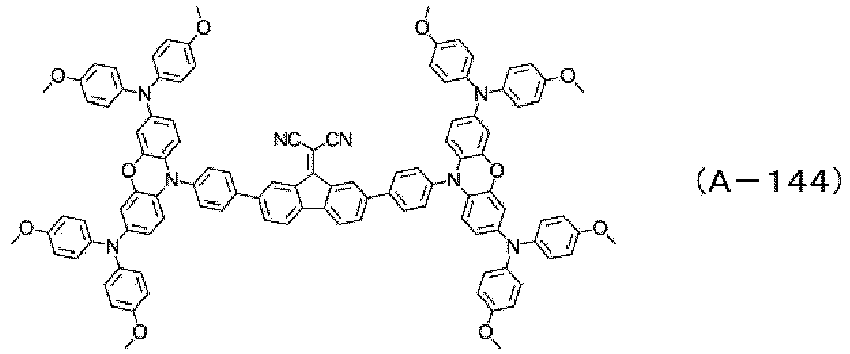
- The compound of the above formula (A-2) (0.6 g), 1,3-diethylthiobarbituric acid (0.38 g, manufactured by Wako Pure Chemical Industries, Ltd.), and THF (24 mL) were placed in a reaction vessel and stirred in an argon atmosphere. Piperidine (0.07 mL) was added thereto. The temperature was raised, and the mixture was heated under reflux for 4 hours. After the reaction was completed, the reaction solution was poured into a beaker containing 300 mL of water. The mixture was filtered, and the residue on the filter was washed with 30 mL of water and with 30 mL of methanol. The resulting crude product was purified using a silica gel column (toluene) to obtain a compound represented by the formula (A-54) below, as a black green powder (actual yield: 0.44 g, percent yield: 60%).
- 1H-NMR (400 MHz, CDCl3): δ (ppm) = 3.81 (12H), 6.85 (8H), 6.98 (4H), 7.10 (8H), 7.43 (4H), 7.53 (2H), 7.67 (2H), 8.41 (2H).

- First, 2,7-dibromofluorenone (0.68 g, manufactured by Tokyo Chemical Industry Co., Ltd.), the compound of the formula (12) below (2.52 g), potassium carbonate (0.72 g, manufactured by Kanto Chemical Co., Inc.), tetrakis(triphenylphosphine)palladium (0.09 g, manufactured by Kanto Chemical Co., Inc.), toluene (11 mL), ethanol (3 mL), and water (3 mL) were placed in a reaction vessel and degassed under reduced pressure. The mixture was stirred for 10 hours while heating under reflux. After the reaction was completed, the reaction solution was put into a beaker containing water (100 mL). Toluene (20 mL) was added thereto, and then liquid-liquid separation was performed. The organic layer was dried over magnesium sulfate and then concentrated. The resulting crude product was purified using a silica gel column (toluene:hexane = 2/1 (volume ratio)) to obtain a compound represented by the formula (A-8) below, as a red powder (actual yield: 1.79 g, percent yield: 84%).
- 1H-NMR (400 MHz, CDCl3): δ (ppm) = 0.92 (12H), 1.31-1.36 (16H), 1.40-1.47 (8H), 1.74-1.81 (8H), 3.94 (8H), 6.84 (8H), 6.98 (4H), 7.08 (8H), 7.43 (4H), 7.52 (2H), 7.60 (2H), 7.86 (2H).

- The compound of the above formula (A-8) (0.68 g), malononitrile (0.22 g, manufactured by Tokyo Chemical Industry Co., Ltd.), and THF (26 mL) were placed in a reaction vessel and stirred in an argon atmosphere. A mixture of acetic acid and pyridine (volume ratio = 1:1) (4.6 mL) was added thereto, and the resulting mixture was stirred for 19 hours while heating under reflux. After the reaction was completed, the reaction solution was poured into water (150 mL). Toluene (20 mL) was added thereto, and liquid-liquid separation was performed. The organic layer was dried over magnesium sulfate and then concentrated. The resulting crude product was purified using a silica gel column (toluene) to obtain a compound represented by the formula (A-20) below, as a black green solid (actual yield: 0.59 g, percent yield: 83%).
- 1H-NMR (400 MHz, CDCl3): δ (ppm) = 0.92 (12H), 1.31-1.36 (16H), 1.40-1.47 (8H), 1.74-1.81 (8H), 3.94 (8H), 6.84 (8H), 6.98 (4H), 7.08 (8H), 7.43 (4H), 7.52 (2H), 7.65 (2H), 8.57 (2H).

- First, a compound represented by the formula (13) below (1.10 g), [4-[bis(4-methoxyphenyl)amino]phenyl]boronic acid (1.75 g, manufactured by Tokyo Chemical Industry Co., Ltd.), potassium carbonate (0.82 g, manufactured by Kanto Chemical Co., Inc.), tetrakis triphenylphosphinepalladium (0.10 g, manufactured by Kanto Chemical Co., Inc.), toluene (18 mL), ethanol (5.1 mL), and water (5.1 mL) were placed in a reaction vessel and degassed under reduced pressure. The mixture was heated under reflux for 6 hours. After the reaction was completed, the reaction solution was cooled to 40°C or below, and water (10 mL) and methanol (10 mL) were added. The resulting mixture was filtered, and the residue on the filter was washed with methanol (10 mL) and dried. The resulting crude product was purified using a silica gel column (chloroform:toluene = 50/1 (volume ratio)) to obtain a compound represented by the formula (A-11) below, as a red powder (actual yield: 1.79 g, percent yield: 86%).
- 1H-NMR (400 MHz, CDCl3): δ (ppm) = 3.81 (12H), 6.86 (8H), 6.93 (4H), 7.09 (8H), 7.18 (2H), 7.34 (2H), 7.42 (4H), 7.50 (2H), 7.71 (2H), 7.92 (2H).

- The compound represented by the above formula (A-11) (0.73 g), malononitrile (0.22 g, manufactured by Tokyo Chemical Industry Co., Ltd.), and THF (26 mL) were placed in a reaction vessel and stirred in an argon atmosphere. A mixture of acetic acid and pyridine (volume ratio = 1:1) (4.6 mL) was added thereto, and the resulting mixture was heated under reflux for 15 hours. After the reaction was completed, the reaction solution was poured into water (150 mL). The resulting mixture was filtered, and the residue on the filter was washed with methanol (20 mL) and then dried. The resulting crude product was purified using a silica gel column (chloroform) to obtain a compound represented by the formula (A-23) below, as a black green solid (actual yield: 0.63 g, percent yield: 83%).
- 1H-NMR (400 MHz, CDCl3): δ (ppm) = 3.81 (12H), 6.87 (8H), 6.93 (4H), 7.09 (8H), 7.18 (2H), 7.34 (2H), 7.42 (4H), 7.60 (2H), 7.90 (2H), 8.65 (2H).

- The compound of the above formula (A-11) (0.45 g), diethyl malonate (0.42 mL, manufactured by Tokyo Chemical Industry Co., Ltd.), and THF (15 mL) were placed in a reaction vessel and stirred in an argon atmosphere. The mixture was cooled to 5°C or below in an ice bath, and pyridine (0.63 mL) was added. The mixture was cooled again to 5°C or below, and titanium tetrachloride (0.32 mL, manufactured by Wako Pure Chemical Industries, Ltd.) was added. The temperature was then raised, and the mixture was heated under reflux for 9 hours. After the reaction was completed, the reaction solution was put into a beaker containing water (150 mL). The resulting mixture was filtered, and the residue on the filter was washed with water (10 mL) and with methanol (30 mL), and dried. The resulting crude product was purified using a silica gel column (chloroform) to obtain a compound represented by the formula (A-36) below, as a brown powder (actual yield: 0.36 g, percent yield: 71%).
- 1H-NMR (400 MHz, THF-ds): δ (ppm) = 1.39 (6H), 3.78 (12H), 4.50 (4H), 6.83-6.90 (12H), 7.05 (8H), 7.24 (2H), 7.35 (2H), 7.45 (4H), 7.71 (4H), 8.20 (2H).

- The compound of the above formula (A-11) (0.45 g), methyl cyanoacetate (0.25 mL, manufactured by Tokyo Chemical Industry Co., Ltd.), and THF (15 mL) were placed in a reaction vessel and stirred in an argon atmosphere. The mixture was cooled to 5°C or below in an ice bath, and pyridine (0.63 mL) was added. The mixture was cooled again to 5°C or below, and titanium tetrachloride (0.32 mL, manufactured by Wako Pure Chemical Industries, Ltd.) was added. The temperature was then raised, and the mixture was heated under reflux for 9 hours. After the reaction was completed, the reaction solution was put into a beaker containing water (150 mL). The resulting mixture was filtered, and the residue on the filter was washed with water (10 mL) and with methanol (30 mL), and dried. The resulting crude product was purified using a silica gel column (chloroform) to obtain a compound represented by the formula (A-49) below, as a brown powder (actual yield: 0.46 g, percent yield: 94%).
- 1H-NMR (400 MHz, THF-ds): δ (ppm) = 3.78 (12H), 4.07 (3H), 6.84-6.89 (12H), 7.05 (8H), 7.24 (2H), 7.37 (1H), 7.40 (1H), 7.45 (4H), 7.71 (4H), 8.43 (1H), 8.92 (1H).

- The compound of the above formula (13) (0.50 g), the compound of the above formula (9) (1.89 g), potassium carbonate (0.37 g, manufactured by Kanto Chemical Co., Inc.), tetrakis triphenylphosphinepalladium (0.05 g, manufactured by Kanto Chemical Co., Inc.), toluene (10 mL), ethanol (2.3 mL), and water (2.3 mL) were placed in a reaction vessel and degassed under reduced pressure. The mixture was heated under reflux for 13 hours. After the reaction was completed, the reaction solution was put into a beaker containing water (100 mL). The resulting mixture was filtered, and the residue on the filter was washed with water (10 mL) and with methanol (30 mL), and dried. The resulting crude product was purified using a silica gel column (toluene:ethyl acetate = 30/1 (volume ratio)) to obtain a compound represented by the formula (A-79) below, as a reddish brown powder (actual yield: 1.23 g, percent yield: 71%).
- 1H-NMR (400 MHz, DMSO-d6): δ (ppm) = 3.70 (24H), 6.82 (16H), 6.88 (16H), 7.09 (4H), 7.32 (4H), 7.64 (6H), 7.67 (4H), 7.70 (2H), 7.84 (2H), 7.89 (2H), 7.94 (6H).

- The compound of the above formula (A-79) (0.66 g), malononitrile (0.11 g, manufactured by Tokyo Chemical Industry Co., Ltd.), and THF (15 mL) were placed in a reaction vessel and stirred in an argon atmosphere. A mixture of acetic acid and pyridine (volume ratio = 1:1) (2.3 mL) was added thereto, and the resulting mixture was heated under reflux for 19 hours. After the reaction was completed, the reaction solution was poured into water (100 mL). The resulting mixture was filtered, and the residue on the filter was washed with methanol (20 mL) and then dried. The resulting crude product was recrystallized (chloroform) to obtain a compound represented by the formula (A-95) below, as a black green solid (actual yield: 0.54 g, percent yield: 80%).
- 1H-NMR (400 MHz, DMSO-d6): δ (ppm) = 3.70 (24H), 6.82 (16H), 6.88 (16H), 7.09 (4H), 7.32 (4H), 7.65 (6H), 7.67 (4H), 7.80 (2H), 7.98 (2H), 8.01 (2H), 8.12 (6H).


- The compound of the above formula (A-79) (0.40 g), diethyl malonate (0.20 mL, manufactured by Tokyo Chemical Industry Co., Ltd.), and THF (9 mL) were placed in a reaction vessel and stirred in an argon atmosphere. The mixture was cooled to 5°C or below in an ice bath, and pyridine (0.31 mL) was added. The mixture was cooled again to 5°C or below, and titanium tetrachloride (0.16 mL, manufactured by Wako Pure Chemical Industries, Ltd.) was added. The temperature was then raised, and the mixture was heated under reflux for 6 hours. After the reaction was completed, the reaction solution was put into a beaker containing water (150 mL). The resulting mixture was filtered, and the residue on the filter was washed with water (10 mL) and with methanol (30 mL), and dried. The resulting crude product was purified using a silica gel column (toluene:ethyl acetate = 20/1 (volume ratio)) to obtain a compound represented by the formula (A-96) below, as a black green powder (actual yield: 0.07 g, percent yield: 16%).
- 1H-NMR (400 MHz, DMSO-d6): δ (ppm) = 1.42 (6H), 3.78 (12H), 4.52 (4H), 6.83-6.91 (20H), 6.88 (16H), 7.40 (4H), 7.62 (6H), 7.65 (4H), 7.68 (2H), 7.80 (2H), 7.85 (2H), 7.89 (6H).


- The compound of the above formula (A-67) (0.30 g), methyl cyanoacetate (0.10 mL, manufactured by Tokyo Chemical Industry Co., Ltd.), and THF (7 mL) were placed in a reaction vessel and stirred in an argon atmosphere. The mixture was cooled to 5°C or below in an ice bath, and pyridine (0.25 mL) was added. The mixture was cooled again to 5°C or below, and titanium tetrachloride (0.13 mL, manufactured by Wako Pure Chemical Industries, Ltd.) was added. The temperature was then raised, and the mixture was heated under reflux for 9 hours. After the reaction was completed, water (20 mL) and toluene (10 mL) were added, and liquid-liquid separation was performed. The organic layer was dried over magnesium sulfate and then concentrated. The resulting crude product was purified using a silica gel column (toluene:ethyl acetate = 40/1 (volume ratio)) to obtain a compound represented by the formula (A-83) below, as a black green powder (actual yield: 0.22 g, percent yield: 70%).
- 1H-NMR (400 MHz, THF-ds): δ (ppm) = 3.71 (24H), 4.06 (3H), 6.74 (16H), 6.93 (16H), 7.11 (4H), 7.33 (4H), 7.69-7.76 (8H), 7.88-7.99 (8H), 8.63 (1H), 9.07 (1H).


- The compound of the above formula (A-67) (0.30 g), diethyl malonate (0.18 mL, manufactured by Tokyo Chemical Industry Co., Ltd.), and THF (7 mL) were placed in a reaction vessel and stirred in an argon atmosphere. The mixture was cooled to 5°C or below in an ice bath, and pyridine (0.25 mL) was added. The mixture was cooled again to 5°C or below, and titanium tetrachloride (0.13 mL, manufactured by Wako Pure Chemical Industries, Ltd.) was added. The temperature was then raised, and the mixture was heated under reflux for 9 hours. After the reaction was completed, water (20 mL) and toluene (10 mL) were added, and liquid-liquid separation was performed. The organic layer was dried over magnesium sulfate and then concentrated. The resulting crude product was purified using a silica gel column (toluene:ethyl acetate = 50/1 (volume ratio)) to obtain a compound represented by the formula (A-155) below, as a black green powder (actual yield: 0.26 g, percent yield: 78%).
- 1H-NMR (400 MHz, THF-ds): δ (ppm) = 1.35 (6H), 3.71 (24H), 4.45 (4H), 6.73 (16H), 6.91 (16H), 7.10 (4H), 7.35 (4H), 7.70-7.72 (8H), 7.84-7.91 (8H), 8.34 (2H).


- A glass substrate with an etched, fluorine-doped tin oxide (FTO) coating (
conductive support 1, manufactured by Solaronix) was ultrasonically cleaned in isopropyl alcohol and then treated with UV/ozone. - Tin(IV) oxide, 15% in H2O colloidal dispersion (manufactured by Alfa Aesar) and purified water were mixed in a volume ratio of 1:3 to obtain a tin oxide dispersion (coating solution for an electron transport layer), and the FTO coating was spin-coated with the coating solution for an electron transport layer. After that, the resultant was heated at 150°C for 30 minutes using a hot plate to form a tin oxide thin film (electron transport layer 2) having a film thickness of about 40 nm.
- Under a nitrogen stream in a glove box, formamidine hydroiodide (1 M, manufactured by Tokyo Chemical Industry Co., Ltd.), lead(II) iodide (1.1 M, manufactured by Tokyo Chemical Industry Co., Ltd.), methylamine hydrobromide (0.2 M, manufactured by Tokyo Chemical Industry Co., Ltd.), and lead(II) bromide (0.2 M, manufactured by Tokyo Chemical Industry Co., Ltd.) were dissolved in a solvent mixture of dimethylformamide and dimethyl sulfoxide in a volume ratio of 4:1. A cesium iodide (1.5 M, manufactured by Tokyo Chemical Industry Co., Ltd.) solution in dimethyl sulfoxide was added thereto such that the amount of cesium added was 5% in terms of the percent composition. Thus, a perovskite precursor solution was prepared.
- Under a nitrogen atmosphere in a glove box, the perovskite precursor solution was dropped on the tin oxide thin film, followed by spin-coating. During the spin-coating, 0.3 mL of chlorobenzene was dropped. Thus, a perovskite precursor film was formed.
- After that, the resultant was heated at 100°C for 1 hour using a hot plate, to thereby form a Cs(MAFA)Pb(IBr)3 layer (light/electricity conversion layer 3) having a film thickness of about 500 nm.
- Under a nitrogen stream in a glove box, 4-tert-butylpyridine and lithium bis(trifluoromethanesulfonyl)imide as dopants were dissolved in chlorobenzene. The compound (A-2), which was a hole transport material obtained in Synthesis Example 1, was dissolved in the dopant solution in chlorobenzene to a concentration of 50 mM. The amounts of 4-tert-butylpyridine and lithium bis(trifluoromethanesulfonyl)imide were adjusted to 3 equivalents and 0.5 equivalents, respectively, with respect to the compound (A-2). Thus, a coating solution for a hole transport layer was obtained.
- Under a nitrogen atmosphere in a glove box, the Cs(MAFA)Pb(IBr)3 layer (light/electricity conversion layer 3) was spin-coated with the coating solution for a hole transport layer, to thereby form a
hole transport layer 4 having a film thickness of about 200 nm. - Vacuum evaporation was performed (degree of vacuum: about 1 × 10⁻⁴ Pa) to form a gold film having a thickness of 80 to 100 nm as a gold electrode (counter electrode 5) on the hole transport layer.
- Thus, a device for converting light into electricity was produced.
- The conductive support side of the device for converting light into electricity was irradiated with simulated sunlight (AM1.5, 100 mW/cm2) generated by a solar simulator (model OTENTO-SUN SH, manufactured by Bunkoukeiki Co., Ltd.), and power conversion efficiency was determined by determining current-voltage characteristics using a source meter (Model 2400 Series SourceMeter, manufactured by KEITHLEY). Table 1 shows the current-voltage characteristics and the power conversion efficiency.
- A device for converting light into electricity was produced in the same manner as in Example 1, except that, instead of the compound (A-2), the compound (A-15) was dissolved in the dopant solution in chlorobenzene to a concentration of 30 mM and used. Then, the power conversion efficiency was determined by determining current-voltage characteristics in the same manner as in Example 1. Table 1 shows the current-voltage characteristics and the power conversion efficiency.
- A device for converting light into electricity was produced in the same manner as in Example 1, except that the compound (A-28) was used instead of the compound (A-2). Then, the power conversion efficiency was determined by determining current-voltage characteristics in the same manner as in Example 1. Table 1 shows the current-voltage characteristics and the power conversion efficiency.
- A device for converting light into electricity was produced in the same manner as in Example 1, except that the compound (A-41) was used instead of the compound (A-2). Then, the power conversion efficiency was determined by determining current-voltage characteristics in the same manner as in Example 1. Table 1 shows the current-voltage characteristics and the power conversion efficiency.
- A device for converting light into electricity was produced in the same manner as in Example 1, except that the compound (A-67) was used instead of the compound (A-2). Then, the power conversion efficiency was determined by determining current-voltage characteristics in the same manner as in Example 1. Table 1 shows the current-voltage characteristics and the power conversion efficiency.
- A device for converting light into electricity was produced in the same manner as in Example 1, except that a standard hole transport material Spiro-OMeTAD (manufactured by Sigma-Aldrich) represented by the formula (B-1) below was used instead of the compound (A-2). Then, the power conversion efficiency was determined by determining current-voltage characteristics in the same manner as in Example 1. Table 1 shows the current-voltage characteristics and the power conversion efficiency.

Table 1 Hole transport material Short-circuit current density Jsc [mA/cm2] Open-circuit voltage Voc [V] Fill factor FF Power conversion efficiency PCE [%] Ex. 1 (A-2) 22.28 1.07 0.72 17.43 Ex. 2 (A-15) 22.61 1.04 0.66 15.81 Ex. 3 (A-28) 20.98 1.13 0.73 17.56 Ex. 4 (A-41) 22.83 1.01 0.67 15.69 Ex. 5 (A-67) 22.30 1.01 0.71 15.98 Com. Ex. 1 (B-1) 22.27 1.00 0.69 15.38 - It can be seen from the results in Table 1 that the devices for converting light into electricity each including, as the hole transport material, the compound (A-2), (A-15), (A-28), (A-41), or (A-67) having the fluorenone skeleton, which is a compound of the present invention, exhibited higher efficiencies in conversion of light into electricity than the device including the compound (B-1), which is a standard hole transport material.
- Glass with FLAT ITO coating (
conductive support 1, manufactured by Geomatic Co., Ltd.) was ultrasonically cleaned in isopropyl alcohol and then treated with UV/ozone. - Tin(IV) oxide, 15% in H2O colloidal dispersion (manufactured by Alfa Aesar) and purified water were mixed in a volume ratio of 1:9 to obtain a tin oxide dispersion (coating solution for an electron transport layer), and the ITO coating was spin coated with the coating solution for an electron transport layer. After that, the resultant was heated at 150°C for 30 minutes using a hot plate to form a tin oxide thin film (electron transport layer 2) having a thickness of about 20 nm.
- Under a nitrogen stream in a glove box, formamidine hydroiodide (1 M, manufactured by Tokyo Chemical Industry Co., Ltd.), lead(II) iodide (1.1 M, manufactured by Tokyo Chemical Industry Co., Ltd.), methylamine hydrobromide (0.2 M, manufactured by Tokyo Chemical Industry Co., Ltd.), and lead(II) bromide (0.2 M, manufactured by Tokyo Chemical Industry Co., Ltd.) were dissolved in a solvent mixture of dimethylformamide and dimethyl sulfoxide in a volume ratio of 4:1. A cesium iodide (1.5 M, manufactured by Tokyo Chemical Industry Co., Ltd.) solution in dimethyl sulfoxide was added thereto such that the amount of cesium added was 5% in terms of the percent composition. Thus, a perovskite precursor solution was prepared.
- Under a nitrogen atmosphere in a glove box, the perovskite precursor solution was dropped onto the tin oxide thin film, followed by spin-coating. During the spin-coating, 0.3 mL of chlorobenzene was dropped. Thus, a perovskite precursor film was formed.
- After that, the resultant was heated at 100°C for 1 hour using a hot plate, to thereby form a Cs(MAFA)Pb(IBr)3 layer (light/electricity conversion layer 3) having a film thickness of about 500 nm.
- Under a nitrogen stream in a glove box, 4-tert-butylpyridine and lithium bis(trifluoromethanesulfonyl)imide as dopants were dissolved in chlorobenzene. The compound (A-36), which was a hole transport material obtained in Synthesis Example 19, was dissolved in the dopant solution in chlorobenzene to a concentration of 30 mM at 60°C. The amounts of 4-tert-butylpyridine and lithium bis(trifluoromethanesulfonyl)imide were adjusted to 3 equivalents and 0.5 equivalents, respectively, with respect to the compound (A-36). Thus, a coating solution for a hole transport layer was obtained.
- Under a nitrogen atmosphere in a glove box, the Cs(MAFA)Pb(IBr)3 layer (light/electricity conversion layer 3) was spin-coated with the coating solution for a hole transport layer, to thereby form a
hole transport layer 4 having a film thickness of about 200 nm. - Vacuum evaporation was performed (degree of vacuum: about 1 × 10⁻⁴ Pa) to form a gold film having a thickness of about 80 nm as a gold electrode (counter electrode 5) on the hole transport layer.
- Thus, a device for converting light into electricity was produced.
- The conductive support side of the device for converting light into electricity was irradiated with simulated sunlight (AM1.5, 100 mW/cm2) generated by a solar simulator (model OTENTO-SUN SH, manufactured by Bunkoukeiki Co., Ltd.), and the initial power conversion efficiency was determined by determining current-voltage characteristics using a source meter (Model 2400 Series SourceMeter, manufactured by KEITHLEY). Table 2 shows the current-voltage characteristics and the initial power conversion efficiency.
- After the determination of the current-voltage characteristics, the device for converting light into electricity was stored in a desiccator containing silica gel for 30 days. Then, current-voltage characteristics were determined again under simulated sunlight irradiation to determine the power conversion efficiency after 30 days.
- The retention (%) was calculated using the formula (a-1) below from the initial power conversion efficiency and time-dependent efficiency, which is the power conversion efficiency after 30 days. Table 2 shows the retention.
[Math. 1]
- A device for converting light into electricity was produced in the same manner as in Example 6, except that, instead of the compound (A-36), the compound (A-49) was dissolved in the dopant solution in chlorobenzene to a concentration of 30 mM at 90°C and used. Then, the initial power conversion efficiency and the power conversion efficiency after 30 days were determined in the same manner as in Example 6. Table 2 shows the initial power conversion efficiency. The retention (%) was calculated using the above formula (a-1) from the power conversion efficiency after 30 days. Table 2 also shows the retention.
- A device for converting light into electricity was produced in the same manner as in Example 6, except that, instead of the compound (A-36), the compound (A-79) was dissolved in the dopant solution in chlorobenzene to a concentration of 30 mM at 90°C and used. Then, the initial power conversion efficiency and the power conversion efficiency after 30 days were determined in the same manner as in Example 6. Table 2 shows the initial power conversion efficiency. The retention (%) was calculated using the above formula (a-1) from the power conversion efficiency after 30 days. Table 2 also shows the retention.
- A device for converting light into electricity was produced in the same manner as in Example 6, except that, instead of the compound (A-36), the compound (A-96) was dissolved in the dopant solution in chlorobenzene to a concentration of 40 mM at room temperature and used. Then, the initial power conversion efficiency and the power conversion efficiency after 30 days were determined in the same manner as in Example 6. Table 2 shows the initial power conversion efficiency. The retention (%) was calculated using the above formula (a-1) from the power conversion efficiency after 30 days. Table 2 also shows the retention.
- A device for converting light into electricity was produced in the same manner as in Example 6, except that, instead of the compound (A-36), the compound (A-155) was dissolved in the dopant solution in chlorobenzene to a concentration of 50 mM at room temperature and used. Then, the initial power conversion efficiency and the power conversion efficiency after 30 days were determined in the same manner as in Example 6. Table 2 shows the initial power conversion efficiency. The retention (%) was calculated using the above formula (a-1) from the power conversion efficiency after 30 days. Table 2 also shows the retention.
- A device for converting light into electricity was produced in the same manner as in Example 6, except that, instead of the compound (A-36), the compound (A-83) was dissolved in the dopant solution in chlorobenzene to a concentration of 50 mM at room temperature and used. Then, the initial power conversion efficiency and the power conversion efficiency after 30 days were determined in the same manner as in Example 6. Table 2 shows the initial power conversion efficiency. The retention (%) was calculated using the above formula (a-1) from the power conversion efficiency after 30 days. Table 2 also shows the retention.
- A device for converting light into electricity was produced in the same manner as in Example 6, except that, instead of the compound (A-36), the compound (A-11) was dissolved in the dopant solution in chlorobenzene to a concentration of 20 mM at 90°C and used. Then, the initial power conversion efficiency and the power conversion efficiency after 30 days were determined in the same manner as in Example 6. Table 2 shows the initial power conversion efficiency. The retention (%) was calculated using the above formula (a-1) from the power conversion efficiency after 30 days. Table 2 also shows the retention.
- A device for converting light into electricity was produced in the same manner as in Example 6, except that, instead of the compound (A-36), a standard hole transport material Spiro-OMeTAD (manufactured by Sigma-Aldrich) represented by the above formula (B-1) was dissolved in the dopant solution in chlorobenzene to a concentration of 50 mM at room temperature and used. Then, the initial power conversion efficiency and the power conversion efficiency after 30 days were determined in the same manner as in Example 6. Table 2 shows the initial power conversion efficiency. The retention (%) was calculated using the above formula (a-1) from the power conversion efficiency after 30 days. Table 2 also shows the retention.
Table 2 Hole transport material Short-circuit current density Jsc [mA/cm2] Open-circuit voltage Voc [V] Fill factor FF Power conversion efficiency PCE [%] Retention [%] Ex. 6 (A-36) 20.77 1.04 0.62 13.32 122.87 Ex. 7 (A-37) 21.97 1.00 0.67 14.79 104.27 Ex. 8 (A-79) 22.46 1.07 0.74 17.96 92.75 Ex. 9 (A-96) 20.76 1.05 0.67 14.66 109.55 Ex. 10 (A-155) 21.84 1.07 0.69 15.98 87.66 Ex. 11 (A-83) 21.80 1.05 0.69 15.82 87.24 Ex. 12 (A-11) 19.72 0.97 0.54 10.31 114.43 Com. Ex. 2 (B-1) 20.11 1.06 0.62 13.26 69.87 - It can be seen from the results in Table 2 that the devices for converting light into electricity each including, as the hole transport material, the compound (A-36), (A-37), (A-79), (A-96), (A-155), or (A-83) having the fluorenone skeleton, which is a compound of the present invention, exhibited higher efficiencies in conversion of light into electricity than the device including the compound (B-1), which is a standard hole transport material.
- It can also be seen from the results in Table 2 that the devices for converting light into electricity each including, as the hole transport material, the compound (A-36), (A-37), (A-79), (A-96), (A-155), (A-83), or (A-11) having the fluorenone skeleton, which is a compound of the present invention, had better storage durability than the device including the compound (B-1), which is a standard hole transport material.
- A device for converting light into electricity that includes the hole transport material according to the present invention has favorable power conversion efficiency, and can thus provide clean energy as a solar cell capable of efficiently converting solar energy into electrical energy. The device for converting light into electricity can also be used in other applications such as organic EL and image sensors.
-
- 1
- Conductive support
- 2
- Electron transport layer
- 3
- Light/electricity conversion layer
- 4
- Hole transport layer
- 5
- Counter electrode
Claims (6)
- A compound represented by the general formula (1) below:
 where R1 to R20 each independently represent a hydrogen atom, a halogen atom, a carboxyl group, a trimethylsilyl group, a linear or branched alkyl group having 1 to 20 carbon atoms and optionally having a substituent, a linear or branched alkenyl group having 2 to 20 carbon atoms and optionally having a substituent, a cycloalkyl group having 3 to 10 carbon atoms and optionally having a substituent, an alkyloxy group having 1 to 20 carbon atoms and optionally having a substituent, a cycloalkyloxy group having 3 to 10 carbon atoms and optionally having a substituent, an acyl group having 1 to 20 carbon atoms and optionally having a substituent, a thio group having 1 to 18 carbon atoms and optionally having a substituent, an amino group having 1 to 20 carbon atoms and optionally having a substituent, an aromatic hydrocarbon group having 6 to 36 carbon atoms and having a substituent, or a heterocyclic group having 5 to 36 ring-forming atoms and optionally having a substituent;R1 and R2; R2 and R3; R3 and R4; R4 and R5; R6 and R7; R7 and R8; R8 and R9; R9 and R10; R11 and R12; R12 and R13; R13 and R14; R14 and R15; R16 and R17; R17 and R18; R18 and R19; and R19 and R20 are, in each combination, optionally bonded to each other to form a ring; and R5 and R6; and R15 and R16 are, in each combination, optionally bonded to each other to form a ring;X1 and X2 each represent a divalent group; andY represents an oxygen atom or CR21R22,where R21 and R22 each independently represent a nitrile group, an acyl group having 1 to 10 carbon atoms and optionally having a substituent, or an alkoxycarbonyl group having 1 to 10 carbon atoms and optionally having a substituent, and R21 and R22 are optionally bonded to each other to form a ring.
 - The compound as set forth in claim 1,wherein, in the general formula (1), X1 and X2 are represented by the general formula (2) below:
 where R23 to R28 each independently represent a hydrogen atom, a linear or branched alkyl group having 1 to 10 carbon atoms and optionally having a substituent, a linear or branched alkenyl group having 2 to 10 carbon atoms and optionally having a substituent, a cycloalkyl group having 3 to 10 carbon atoms and optionally having a substituent, an aromatic hydrocarbon group having 6 to 18 carbon atoms and optionally having a substituent, or a heterocyclic group having 5 to 18 ring-forming atoms and optionally having a substituent;R23 and R24; R25 and R26; and R27 and R28 are, in each combination, optionally bonded to each other to form a ring;Z represents an oxygen atom, a sulfur atom, or a selenium atom; andm and n represent integers of 0 to 2, with the proviso that cases where both m and n are 0 are excluded.
 - The compound as set forth in claim 2,
wherein, in the general formula (2), m is 1. - The compound as set forth in any one of claims 1 to 3,
wherein, in the general formula (1), R1 to R20 are each independently a hydrogen atom, a linear or branched alkyl group having 1 to 20 carbon atoms and optionally having a substituent, an alkoxy group having 1 to 20 carbon atoms and optionally having a substituent, a thio group having 1 to 18 carbon atoms and optionally having a substituent, or an amino group having 1 to 20 carbon atoms and optionally having a substituent. - A hole transport material comprising the compound as set forth in any one of claims 1 to 4.
- A device for converting light into electricity, comprising the hole transport material as set forth in claim 5.
Applications Claiming Priority (2)
| Application Number | Priority Date | Filing Date | Title |
|---|---|---|---|
| JP2021002801 | 2021-01-12 | ||
| PCT/JP2022/000486 WO2022153962A1 (en) | 2021-01-12 | 2022-01-11 | Compound, hole transport material, and photoelectric conversion element including same |
Publications (2)
| Publication Number | Publication Date |
|---|---|
| EP4279481A1 true EP4279481A1 (en) | 2023-11-22 |
| EP4279481A4 EP4279481A4 (en) | 2024-12-11 |
Family
ID=82446311
Family Applications (1)
| Application Number | Title | Priority Date | Filing Date |
|---|---|---|---|
| EP22739369.1A Withdrawn EP4279481A4 (en) | 2021-01-12 | 2022-01-11 | COMPOUND, HOLE TRANSPORT MATERIAL AND PHOTOELECTRIC CONVERSION ELEMENT THEREFOR |
Country Status (7)
| Country | Link |
|---|---|
| US (1) | US12279523B2 (en) |
| EP (1) | EP4279481A4 (en) |
| JP (1) | JP7711106B2 (en) |
| KR (1) | KR20230130623A (en) |
| CN (1) | CN116710428B (en) |
| TW (1) | TWI912444B (en) |
| WO (1) | WO2022153962A1 (en) |
Families Citing this family (6)
| Publication number | Priority date | Publication date | Assignee | Title |
|---|---|---|---|---|
| JP7856459B2 (en) * | 2022-03-25 | 2026-05-11 | 保土谷化学工業株式会社 | Compounds, hole transport materials, and photoelectric conversion elements using the same |
| CN115322164B (en) * | 2022-08-03 | 2023-09-01 | 华南师范大学 | Novel D1-D2-A compound and application thereof |
| CN115440894A (en) * | 2022-09-29 | 2022-12-06 | 无锡极电光能科技有限公司 | A kind of electron transport film layer and application |
| CN118084696B (en) * | 2024-01-22 | 2025-08-05 | 南阳师范学院 | A fluorescent probe, a synthesis method and its application in detecting hydroxyl-containing solvents |
| TW202603081A (en) * | 2024-03-27 | 2026-01-16 | 美商凱樂仕股份有限公司 | Precursor solutions for perovskite solar cells |
| CN121285164A (en) * | 2024-07-03 | 2026-01-06 | 宁德时代未来能源(上海)研究院有限公司 | Solar cell, power generation device and power utilization device |
Family Cites Families (12)
| Publication number | Priority date | Publication date | Assignee | Title |
|---|---|---|---|---|
| US4576886A (en) | 1984-02-13 | 1986-03-18 | Konishiroku Photo Industry Co., Ltd. | Azo photoreceptor |
| CN102214800B (en) * | 2011-05-20 | 2013-07-24 | 电子科技大学 | White-light organic luminescent device and manufacturing method thereof |
| CN108368136A (en) | 2015-12-16 | 2018-08-03 | 国立大学法人京都大学 | Complex compound and perovskite material, and perovskite solar cell using the complex compound or perovskite material |
| CN107046100B (en) * | 2016-04-25 | 2018-12-28 | 中节能万润股份有限公司 | A kind of organic electroluminescence device and its application containing disubstituted -9-Fluorenone compound |
| CN106467485B (en) | 2016-08-24 | 2020-04-03 | 中节能万润股份有限公司 | A kind of compound with 9-fluorenone as the core and its application |
| CN106467529B (en) | 2016-08-24 | 2019-06-14 | 江苏三月光电科技有限公司 | An organic electroluminescent material with 9-fluorenone as the core and its application |
| CN108675941B (en) | 2018-04-13 | 2020-07-10 | 华中科技大学 | An undoped hole transport material based on dicyanofluoranthene |
| CN108586289B (en) * | 2018-05-04 | 2020-12-29 | 西北大学 | Malononitrile-substituted aryl anthracene phenanthrene-based organic electroluminescent material, preparation method and application thereof |
| CN109180528A (en) | 2018-09-30 | 2019-01-11 | 长春海谱润斯科技有限公司 | A kind of triarylamine derivative and its organic electroluminescence device |
| CN109574917B (en) | 2018-12-03 | 2020-12-08 | 武汉尚赛光电科技有限公司 | Fluorenone derivative and preparation and application thereof |
| CN110627667B (en) | 2019-09-23 | 2022-08-30 | 南京烯勒光电科技有限公司 | Dumbbell-type hole transport material, synthesis method and perovskite solar cell |
| CN113087726A (en) | 2021-02-24 | 2021-07-09 | 浙江大学 | Arylamine organic semiconductor material and application thereof in photoelectric device |
-
2022
- 2022-01-11 CN CN202280008549.8A patent/CN116710428B/en active Active
- 2022-01-11 KR KR1020237020510A patent/KR20230130623A/en active Pending
- 2022-01-11 US US18/269,881 patent/US12279523B2/en active Active
- 2022-01-11 JP JP2022575578A patent/JP7711106B2/en active Active
- 2022-01-11 EP EP22739369.1A patent/EP4279481A4/en not_active Withdrawn
- 2022-01-11 WO PCT/JP2022/000486 patent/WO2022153962A1/en not_active Ceased
- 2022-01-12 TW TW111101221A patent/TWI912444B/en active
Also Published As
| Publication number | Publication date |
|---|---|
| US12279523B2 (en) | 2025-04-15 |
| US20240099128A1 (en) | 2024-03-21 |
| CN116710428A (en) | 2023-09-05 |
| EP4279481A4 (en) | 2024-12-11 |
| JPWO2022153962A1 (en) | 2022-07-21 |
| TW202237552A (en) | 2022-10-01 |
| KR20230130623A (en) | 2023-09-12 |
| CN116710428B (en) | 2025-08-19 |
| TWI912444B (en) | 2026-01-21 |
| JP7711106B2 (en) | 2025-07-22 |
| WO2022153962A1 (en) | 2022-07-21 |
Similar Documents
| Publication | Publication Date | Title |
|---|---|---|
| JP7711106B2 (en) | Compound, hole transport material, and photoelectric conversion element using the same | |
| JP7695249B2 (en) | Compound, hole transport material for photoelectric conversion element, hole transport layer, and photoelectric conversion element and solar cell using the same | |
| JP7735108B2 (en) | Compound, hole transport material for photoelectric conversion element, and photoelectric conversion element and solar cell using the same | |
| JP2021163968A (en) | Hole transport layer for photoelectric conversion element, photoelectric conversion element using it, and perovskite type solar cell | |
| JP7767042B2 (en) | Compound, hole transport material, and photoelectric conversion element using the same | |
| JP2022058213A (en) | Compound with 1,3-dithiol skeleton, and photoelectric conversion element employing that compound | |
| JP7856459B2 (en) | Compounds, hole transport materials, and photoelectric conversion elements using the same | |
| KR20250165376A (en) | Compounds, hole transport materials, and photoelectric conversion devices using the same | |
| EP4412427A1 (en) | Compound having sulfonate group, hole-transporting material, hole-transporting material composition for photoelectric conversion element, photoelectric conversion element and solar cell | |
| JP7842081B2 (en) | Compounds having a sulfonic acid base, and photoelectric conversion elements using the compound. | |
| EP4676197A1 (en) | Material for hole transportation layer, and photoelectric conversion element and compound using same | |
| WO2023054344A1 (en) | Compound, hole transport material, and photoelectric conversion element using same | |
| JP2024051648A (en) | Compound, hole transport material, and photoelectric conversion element using the same | |
| JP2025060472A (en) | Compound, hole transport material, and photoelectric conversion element using the same | |
| WO2025070756A1 (en) | Compound, hole transport material, and photoelectric conversion element using same | |
| JP2024130904A (en) | Compound, hole transport material, and photoelectric conversion element using the same | |
| JP2026076122A (en) | Compound, hole transport material, and photoelectric conversion element using the hole transport material | |
| WO2024071042A1 (en) | Compound, hole transport material, and photoelectric conversion element using said compound |
Legal Events
| Date | Code | Title | Description |
|---|---|---|---|
| STAA | Information on the status of an ep patent application or granted ep patent |
Free format text: STATUS: THE INTERNATIONAL PUBLICATION HAS BEEN MADE |
|
| PUAI | Public reference made under article 153(3) epc to a published international application that has entered the european phase |
Free format text: ORIGINAL CODE: 0009012 |
|
| STAA | Information on the status of an ep patent application or granted ep patent |
Free format text: STATUS: REQUEST FOR EXAMINATION WAS MADE |
|
| 17P | Request for examination filed |
Effective date: 20230626 |
|
| AK | Designated contracting states |
Kind code of ref document: A1 Designated state(s): AL AT BE BG CH CY CZ DE DK EE ES FI FR GB GR HR HU IE IS IT LI LT LU LV MC MK MT NL NO PL PT RO RS SE SI SK SM TR |
|
| DAV | Request for validation of the european patent (deleted) | ||
| DAX | Request for extension of the european patent (deleted) | ||
| A4 | Supplementary search report drawn up and despatched |
Effective date: 20241113 |
|
| RIC1 | Information provided on ipc code assigned before grant |
Ipc: C07D 239/66 20060101ALI20241107BHEP Ipc: C07D 265/38 20060101ALI20241107BHEP Ipc: C07D 209/88 20060101ALI20241107BHEP Ipc: C07D 409/14 20060101ALI20241107BHEP Ipc: C07D 333/24 20060101ALI20241107BHEP Ipc: C07D 333/22 20060101ALI20241107BHEP Ipc: C07D 279/22 20060101ALI20241107BHEP Ipc: C07C 255/42 20060101ALI20241107BHEP Ipc: C07C 229/44 20060101ALI20241107BHEP Ipc: C07C 225/22 20060101AFI20241107BHEP |
|
| STAA | Information on the status of an ep patent application or granted ep patent |
Free format text: STATUS: EXAMINATION IS IN PROGRESS |
|
| 17Q | First examination report despatched |
Effective date: 20251216 |
|
| STAA | Information on the status of an ep patent application or granted ep patent |
Free format text: STATUS: THE APPLICATION HAS BEEN WITHDRAWN |
|
| 18W | Application withdrawn |
Effective date: 20260120 |