EP4276858A1 - Bearing structure for high-low-voltage conversion circuit - Google Patents
Bearing structure for high-low-voltage conversion circuit Download PDFInfo
- Publication number
- EP4276858A1 EP4276858A1 EP22186888.8A EP22186888A EP4276858A1 EP 4276858 A1 EP4276858 A1 EP 4276858A1 EP 22186888 A EP22186888 A EP 22186888A EP 4276858 A1 EP4276858 A1 EP 4276858A1
- Authority
- EP
- European Patent Office
- Prior art keywords
- conductor layer
- trench
- bearing structure
- insulation material
- peripheral edge
- Prior art date
- Legal status (The legal status is an assumption and is not a legal conclusion. Google has not performed a legal analysis and makes no representation as to the accuracy of the status listed.)
- Pending
Links
- 238000006243 chemical reaction Methods 0.000 title claims abstract description 40
- 239000004020 conductor Substances 0.000 claims abstract description 125
- 239000012774 insulation material Substances 0.000 claims abstract description 76
- 230000002093 peripheral effect Effects 0.000 claims abstract description 56
- 238000009413 insulation Methods 0.000 claims abstract description 15
- 230000005684 electric field Effects 0.000 claims description 33
- 239000012530 fluid Substances 0.000 claims description 15
- 238000002955 isolation Methods 0.000 claims description 7
- 239000003822 epoxy resin Substances 0.000 claims description 6
- 229920000647 polyepoxide Polymers 0.000 claims description 6
- 229920002635 polyurethane Polymers 0.000 claims description 6
- 239000004814 polyurethane Substances 0.000 claims description 6
- 229920002050 silicone resin Polymers 0.000 claims description 6
- 229920002379 silicone rubber Polymers 0.000 claims description 6
- 239000004945 silicone rubber Substances 0.000 claims description 6
- 239000010410 layer Substances 0.000 description 90
- 238000013461 design Methods 0.000 description 5
- 229910052782 aluminium Inorganic materials 0.000 description 4
- XAGFODPZIPBFFR-UHFFFAOYSA-N aluminium Chemical compound [Al] XAGFODPZIPBFFR-UHFFFAOYSA-N 0.000 description 4
- 238000007789 sealing Methods 0.000 description 4
- 238000012360 testing method Methods 0.000 description 4
- 230000004308 accommodation Effects 0.000 description 3
- 238000004519 manufacturing process Methods 0.000 description 3
- 238000000034 method Methods 0.000 description 3
- 239000007787 solid Substances 0.000 description 3
- 230000015572 biosynthetic process Effects 0.000 description 2
- 230000005611 electricity Effects 0.000 description 2
- HCHKCACWOHOZIP-UHFFFAOYSA-N Zinc Chemical compound [Zn] HCHKCACWOHOZIP-UHFFFAOYSA-N 0.000 description 1
- 230000008033 biological extinction Effects 0.000 description 1
- 230000015556 catabolic process Effects 0.000 description 1
- 239000011247 coating layer Substances 0.000 description 1
- 238000004891 communication Methods 0.000 description 1
- 238000011161 development Methods 0.000 description 1
- 230000000694 effects Effects 0.000 description 1
- 230000017525 heat dissipation Effects 0.000 description 1
- 239000000463 material Substances 0.000 description 1
- 229910052751 metal Inorganic materials 0.000 description 1
- 239000002184 metal Substances 0.000 description 1
- 230000007847 structural defect Effects 0.000 description 1
- 238000009423 ventilation Methods 0.000 description 1
- 229910052725 zinc Inorganic materials 0.000 description 1
- 239000011701 zinc Substances 0.000 description 1
Images




Classifications
-
- H—ELECTRICITY
- H05—ELECTRIC TECHNIQUES NOT OTHERWISE PROVIDED FOR
- H05K—PRINTED CIRCUITS; CASINGS OR CONSTRUCTIONAL DETAILS OF ELECTRIC APPARATUS; MANUFACTURE OF ASSEMBLAGES OF ELECTRICAL COMPONENTS
- H05K7/00—Constructional details common to different types of electric apparatus
- H05K7/02—Arrangements of circuit components or wiring on supporting structure
- H05K7/06—Arrangements of circuit components or wiring on supporting structure on insulating boards, e.g. wiring harnesses
-
- H—ELECTRICITY
- H05—ELECTRIC TECHNIQUES NOT OTHERWISE PROVIDED FOR
- H05K—PRINTED CIRCUITS; CASINGS OR CONSTRUCTIONAL DETAILS OF ELECTRIC APPARATUS; MANUFACTURE OF ASSEMBLAGES OF ELECTRICAL COMPONENTS
- H05K9/00—Screening of apparatus or components against electric or magnetic fields
- H05K9/0067—Devices for protecting against damage from electrostatic discharge
-
- H—ELECTRICITY
- H05—ELECTRIC TECHNIQUES NOT OTHERWISE PROVIDED FOR
- H05K—PRINTED CIRCUITS; CASINGS OR CONSTRUCTIONAL DETAILS OF ELECTRIC APPARATUS; MANUFACTURE OF ASSEMBLAGES OF ELECTRICAL COMPONENTS
- H05K7/00—Constructional details common to different types of electric apparatus
- H05K7/02—Arrangements of circuit components or wiring on supporting structure
-
- H—ELECTRICITY
- H05—ELECTRIC TECHNIQUES NOT OTHERWISE PROVIDED FOR
- H05K—PRINTED CIRCUITS; CASINGS OR CONSTRUCTIONAL DETAILS OF ELECTRIC APPARATUS; MANUFACTURE OF ASSEMBLAGES OF ELECTRICAL COMPONENTS
- H05K7/00—Constructional details common to different types of electric apparatus
- H05K7/14—Mounting supporting structure in casing or on frame or rack
- H05K7/1422—Printed circuit boards receptacles, e.g. stacked structures, electronic circuit modules or box like frames
- H05K7/1427—Housings
- H05K7/1432—Housings specially adapted for power drive units or power converters
-
- H—ELECTRICITY
- H05—ELECTRIC TECHNIQUES NOT OTHERWISE PROVIDED FOR
- H05K—PRINTED CIRCUITS; CASINGS OR CONSTRUCTIONAL DETAILS OF ELECTRIC APPARATUS; MANUFACTURE OF ASSEMBLAGES OF ELECTRICAL COMPONENTS
- H05K7/00—Constructional details common to different types of electric apparatus
- H05K7/18—Construction of rack or frame
-
- H—ELECTRICITY
- H05—ELECTRIC TECHNIQUES NOT OTHERWISE PROVIDED FOR
- H05K—PRINTED CIRCUITS; CASINGS OR CONSTRUCTIONAL DETAILS OF ELECTRIC APPARATUS; MANUFACTURE OF ASSEMBLAGES OF ELECTRICAL COMPONENTS
- H05K1/00—Printed circuits
- H05K1/02—Details
- H05K1/0284—Details of three-dimensional rigid printed circuit boards
-
- H—ELECTRICITY
- H05—ELECTRIC TECHNIQUES NOT OTHERWISE PROVIDED FOR
- H05K—PRINTED CIRCUITS; CASINGS OR CONSTRUCTIONAL DETAILS OF ELECTRIC APPARATUS; MANUFACTURE OF ASSEMBLAGES OF ELECTRICAL COMPONENTS
- H05K2201/00—Indexing scheme relating to printed circuits covered by H05K1/00
- H05K2201/07—Electric details
- H05K2201/0753—Insulation
- H05K2201/0761—Insulation resistance, e.g. of the surface of the PCB between the conductors
-
- H—ELECTRICITY
- H05—ELECTRIC TECHNIQUES NOT OTHERWISE PROVIDED FOR
- H05K—PRINTED CIRCUITS; CASINGS OR CONSTRUCTIONAL DETAILS OF ELECTRIC APPARATUS; MANUFACTURE OF ASSEMBLAGES OF ELECTRICAL COMPONENTS
- H05K2201/00—Indexing scheme relating to printed circuits covered by H05K1/00
- H05K2201/09—Shape and layout
- H05K2201/09009—Substrate related
- H05K2201/09036—Recesses or grooves in insulating substrate
-
- H—ELECTRICITY
- H05—ELECTRIC TECHNIQUES NOT OTHERWISE PROVIDED FOR
- H05K—PRINTED CIRCUITS; CASINGS OR CONSTRUCTIONAL DETAILS OF ELECTRIC APPARATUS; MANUFACTURE OF ASSEMBLAGES OF ELECTRICAL COMPONENTS
- H05K2201/00—Indexing scheme relating to printed circuits covered by H05K1/00
- H05K2201/09—Shape and layout
- H05K2201/09009—Substrate related
- H05K2201/09045—Locally raised area or protrusion of insulating substrate
-
- H—ELECTRICITY
- H05—ELECTRIC TECHNIQUES NOT OTHERWISE PROVIDED FOR
- H05K—PRINTED CIRCUITS; CASINGS OR CONSTRUCTIONAL DETAILS OF ELECTRIC APPARATUS; MANUFACTURE OF ASSEMBLAGES OF ELECTRICAL COMPONENTS
- H05K2201/00—Indexing scheme relating to printed circuits covered by H05K1/00
- H05K2201/09—Shape and layout
- H05K2201/09818—Shape or layout details not covered by a single group of H05K2201/09009 - H05K2201/09809
- H05K2201/0999—Circuit printed on or in housing, e.g. housing as PCB; Circuit printed on the case of a component; PCB affixed to housing
Definitions
- the present disclosure relates to a bearing structure, and more particularly to a bearing structure for a high-low-voltage conversion circuit, so as to avoid the corona and partial discharge due to a high electric field strength on the outer peripheral edge of the conductor.
- a plurality of power conversion modules are disposed in a single system cabinet.
- Each power conversion module needs to be carried on an isolation carrier and be integrated into the system cabinet. Since a high-low voltage conversion circuit is contained in this kind of power conversion module, when the high-voltage circuit and the low-voltage circuit of the high-low conversion circuit are isolated through the isolation carrier, the isolation carrier is further spatially corresponding to a high electric field strength formed due to the voltage difference. Therefore, in order to carry under the action of high electric field strength, the isolation carrier has to avoid the repeated breakdown and extinction phenomenon of partial discharge caused by the structural defects.
- the high-voltage circuit and the low-voltage circuit are disposed and corresponding to the conductor layer with a uniform electric field, respectively.
- the phenomenon of the corona and partial discharge is generated easily on the outer peripheral edge of the conductor layer.
- An object of the present disclosure is to provide a bearing structure configured to carry a high-low-voltage conversion circuit with high electric field strength.
- Another object of the present disclosure is to provide a bearing structure configured to carry and isolate a high-voltage circuit and a low-voltage circuit.
- the bearing structure is made of an insulation material with a dielectric strength greater than 18 kV/mm.
- a high-voltage circuit and a low-voltage circuit with a voltage difference ranged from 10 kV to 30 kV are isolated through the bearing structure, the outer peripheral edge of the conductor layer is sealed by the trench and the insulation material. A distance is maintained between the outer peripheral edge of the conductor layer and an outer surface of the insulation material and greater than 0.6 mm. An air electric field strength on the outer surface of the insulation material is reduced and less than 2.0 kV/mm.
- the bearing structure when the trench and the insulation material are disposed on a peripheral wall formed by the protruding portion, it allows the bearing structure to form an upper half shell or a lower half shell.
- two bearing structures are utilized to form two symmetrical half shells and assembled as a bearing housing.
- the high-voltage circuit is sandwiched between the two symmetrical half shells, and the low-voltage circuit is placed outside the bearing housing, so as to achieve a unit assembly of the power conversion module with small volume. It facilitates to ensure the safety of the solid-state transformer application and enhance the competitiveness of the product.
- a further object of the present disclosure is to provide a bearing structure configured to carry a power conversion module with high electric field strength.
- the bearing structure having the outer peripheral edge of the conductor layer sealed through the designed trench is allowed to be applied to the bearing housing, which are detached into two symmetrical half shells.
- the insulation material is filled into the trench by fluid dispensing, which is easily integrated into the manufacturing process of the two symmetrical half shells carrying the power conversion module. The entire space is not increased. Thus, the safety specifications and the convenience of the bearing housing for the power conversion module are improved effectively.
- a bearing structure configured to carry a high-low-voltage conversion circuit.
- the bearing structure includes an insulation carrier, a first conductor layer, a second conductor layer a first trench and a first insulation material.
- the insulation carrier includes a first surface and a second surface opposite to each other.
- the first conductor layer and a second conductor layer are coated on the first surface and the second surface, respectively.
- a voltage difference is formed between the first conductor layer and the second conductor layer.
- the first trench is disposed on the first surface and surrounds an outer peripheral edge of the first conductor layer.
- the first conductor layer is extended from the first surface into the first trench, and the outer peripheral edge of the first conductor layer is located at a bottom of the first trench.
- the first insulation material covers the outer peripheral edge of the first conductor layer and is filled in the first trench.
- first and second features are formed in direct contact
- additional features may be formed between the first and second features, such that the first and second features may not be in direct contact
- present disclosure may repeat reference numerals and/or letters in the various examples. This repetition is for the purpose of simplicity and clarity and does not in itself dictate a relationship between the various embodiments and/or configurations discussed.
- spatially relative terms such as “upper,” “lower,” “top,” “bottom” and the like, may be used herein for ease of description to describe one element or feature's relationship to another element(s) or feature(s) as illustrated in the figures.
- the spatially relative terms are intended to encompass different orientations of the device in use or operation in addition to the orientation depicted in the figures.
- the apparatus may be otherwise oriented (rotated 90 degrees or at other orientations) and the spatially relative descriptors used herein may likewise be interpreted accordingly.
- the word "about” means within an acceptable standard error of ordinary skill in the art-recognized average.
- all of the numerical ranges, amounts, values and percentages such as the number for the herein disclosed materials, time duration, temperature, operating conditions, the ratio of the amount, and the like, should be understood as the word “about” decorator. Accordingly, unless otherwise indicated, the numerical parameters of the present invention and scope of the appended patent proposed is to follow changes in the desired approximations. At least, the number of significant digits for each numerical parameter should at least be reported and explained by conventional rounding technique is applied. Herein, it can be expressed as a range between from one endpoint to the other or both endpoints. Unless otherwise specified, all ranges disclosed herein are inclusive.
- FIG. 1 is a perspective view illustrating a bearing structure utilized to form a bearing housing according to an embodiment of the present disclosure.
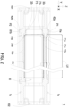
- FIG. 2 is a cross-section view illustrating the bearing structure utilized to form the bearing housing and configured to carry a high-low-voltage conversion circuit according to the embodiment of the present disclosure.
- FIG. 3 is a perspective view illustrating the bearing structure utilized to form the bearing housing with the upper half shell and the lower half shell disassembled according to the embodiment of the present disclosure.
- a bearing structure 1a or a bearing structure 1b is configured to carry a high-low-voltage conversion circuit.
- the bearing housing 1 formed by the bearing structure 1a and the bearing structure 1b is applied in the field of the solid state transformer (SST), so as to simplify the carrying and assembling procedures of the power conversion module in the solid state transformer. At the same time, it ensures that each unit of the power conversion module meets the safety specifications and avoids the phenomenon of corona and partial discharge caused by the high electric field strength.
- the present disclosure is not limited thereto.
- the bearing structure 1a is an upper half shell
- the bearing structure 1b is a lower half shell
- the upper half shell and the lower half shell are symmetrical and assembled with each other to form a bearing housing 1 having an accommodation space 10.
- the bearing housing 1 includes a front opening 101 and a rear opening 102.
- the front opening 101 and the rear opening 102 are in fluid communication with each other through the accommodation space 10, so as to facilitates the bearing housing 1 to accommodate a high-voltage circuit HV and provide the functions of ventilation and heat dissipation.
- the present disclosure is not limited thereto.
- the bearing housing 1 is utilized to carry one unit of the high-low-voltage conversion circuit, the high-voltage circuit HV is sandwiched between the upper half shell of the bearing structure 1a and the lower half shell of the bearing structure 1b, and the low-voltage circuit LV is disposed on an outer side of the bearing housing 1.
- the low-voltage circuit LV is disposed on the top of the upper half shell of the bearing structure 1a.
- a plurality of units of the power conversion modules are carried on a plurality of bearing housings 1, respectively, and then stacked with each other.
- the high-voltage circuit HV accommodated with a bearing housing 1 and the low-voltage circuit LV disposed outside another bearing housing 1 have a voltage difference formed between the lower half shell of the bearing structure 1b.
- the bearing structure 1a and the bearing structure 1b of the present disclosure are not limited to be served as an upper half shell or a lower half shell, and described here firstly.
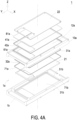
- FIGS. 4A and 4B are partial exploded views illustrating the upper half shell of the bearing housing formed by the bearing structure according to the embodiment of the present disclosure.
- FIG. 5 is an enlarged view showing the region P1 in FIG. 2 .
- the bearing structure 1a is configured to form an upper half shell.
- the bearing structure 1a includes an insulation carrier 10a, a first conductor layer 31a, a second conductor layer 41a, a first trench 51a and a first insulation material 71a.
- the insulation carrier 10a includes a first surface 11a and a second surface 12a opposite to each other.
- the first conductor layer 31a and the second conductor layer 41a are the zinc metal coating layers and coated on the first surface 11a and the second surface 12a, respectively.
- a voltage difference is formed between the first conductor layer 31a and the second conductor layer 41a.
- the high-voltage circuit HV is disposed on a first aluminum plate 21 over the first conductor layer 31a, and the first aluminum plate 21 is spatially corresponding to the first conductor layer 31a, so that the electric field generated by the high-voltage circuit HV is uniformized through the action of the first conductor layer 31a.
- the low-voltage circuit LV is disposed on a second aluminum plate 22 over the second conductor layer 41a, and the second aluminum plate 22 is spatially corresponding to the second conductor layer 41a, so that the electric field generated by the low-voltage circuit LV is uniformized through the action of the second conductor layer 41a.
- the voltage difference of the high-voltage circuit HV and the low-voltage circuit LV is formed between the first conductor layer 31a and the second conductor layer 41a.
- the types of the high-voltage circuit HV formed on the first surface 11a and the low-voltage circuit LV formed on the second surface 12a are not limited in the present disclosure.
- the voltage difference formed between the high-voltage circuit HV and the low-voltage circuit LV is ranged from 10 kV to 30 kV, but the present disclosure is not limited there.
- the first trench 51a is disposed on the first surface 11a and surrounds an outer peripheral edge 32a of the first conductor layer 31a.
- the first conductor layer 31a is coated on the first surface 11a and extended into the first trench 51a, so that the outer peripheral edge 32a of the first conductor layer 31a is located at a bottom 52a of the first trench 51a.
- the first insulation material 71a covers the outer peripheral edge 32a of the first conductor layer 31a and filled in the first trench 51a.
- the voltage difference formed between the high-voltage circuit HV and the low-voltage circuit LV is ranged from 10 kV to 30 kV
- the first insulation material 71a is one selected from the group consisting of an epoxy resin, a silicone rubber, a silicone resin and a polyurethane. Moreover, the first insulation material 71a has a dielectric strength greater than 18 kV/mm. Preferably but not exclusively, in the embodiment, the first insulation material 71a is filled into the first trench 51a by fluid dispensing, so that an outer surface 72a of the first insulation material 71a is coplanar with the opening of the first trench 51a.
- an air electric field strength on the outer surface 72a of the first insulation material 71a is less than 2.0 kV/mm. It avoids the occurrence of corona and partial discharge due to the contact of the air and the outer peripheral edge 32a of the first conductor layer 31a under the high electric field strength.
- the bearing structure 1a is constructed on the upper half shell of the supporting housing 1, and the bearing structure 1a further includes a first protruding portion 13a, which is protruded from the first surface 11a in a direction (i.e., the reverse Z axial direction) away the second surface 12a.
- the first trench 51a is disposed on the first protruding portion 13a.
- the first conductor layer 31a is coated and disposed on the first surface 11a and a lateral wall 131a and a top surface 132a of the first protruding portion 13a, and extended into the bottom 52a of the first trench 51a.
- the lateral-wall structure of the first protruding portion 13a is helpful of performing the fluid dispensing, and preventing the fluid that is not solidified to form the first insulation material 71a from overflowing everywhere.
- the outer surface 72a of the first insulation material 71a and the top surface 132a of the first protruding portion 13a are coplanar. Certainly, the present disclosure is not limited thereto.
- the bearing structure 1a further includes a second trench 61a and a second insulation material 81a.
- the second trench 61a is disposed on the second surface 12a and surrounds an outer peripheral edge 42a of the second conductor layer 41a.
- the second conductor layer 41a is coated on the second surface 12a and extended into the second trench 61a, so that the outer peripheral edge 42a of the second conductor layer 41a is located at a bottom 62a of the second trench 61a.
- the second insulation material 81a is filled in the second trench 61a, and covers the outer peripheral edge 42a of the second conductor layer 41a.
- the bearing structure 1a further includes a second protruding portion 14a, which is protruded from the second surface 12a in a direction (i.e. the Z axial direction) away the first surface 11a.
- the second trench 61a is disposed on the second protruding portion 14a.
- the second conductor layer 41a is coated and disposed on the second surface 12a and a lateral wall 141a and a top surface 142a of the second protruding portion 14a, and extended into the bottom 62a of the second trench 61a.
- the lateral-wall structure of the second protruding portion 14a is helpful of performing the fluid dispensing, and preventing the fluid that is not solidified to form the second insulation material 81a from overflowing everywhere.
- the outer surface 82a of the second insulation material 81a and the top surface 142a of the second protruding portion 14a are coplanar.
- the voltage difference formed between the high-voltage circuit HV and the low-voltage circuit LV is ranged from 10 kV to 30 kV.
- the second insulation material 81a is one selected from the group consisting of an epoxy resin, a silicone rubber, a silicone resin and a polyurethane. Moreover, the second insulation material 81a has a dielectric strength greater than 18 kV/mm. Since the outer peripheral edge 42a of the second conductor layer 41a is sealed through the second trench 61a and the second insulation material 81a, and a distance D2 is maintained between the outer peripheral edge 42a of the second conductor layer 41a and the outer surface 82a of the second insulation material 81a and greater than 0.6 mm. According to the result of the partial discharge test, an air electric field strength on the outer surface 82a of the second insulation material 81a is less than 2.0 kV/mm. It avoids the occurrence of corona and partial discharge due to the contact of the air and the outer peripheral edge 42a of the second conductor layer 41a under the high electric field strength.
- the heights of the first protruding portion 13a and/or the second protruding portion 14a are adjustable according to the practical requirements.
- the first protruding portion 13a and/or the second protruding portion 14a are omitted.
- the first trench 51a is recessed directly from the first surface 11a toward the second surface 12a (i.e. in the Z axial direction).
- the first conductor layer 31a is coated and disposed on the first surface 11a, and extended directly from the first surface 11a to the bottom 52a of the first trench 51a.
- the first insulation material 71a covers the outer peripheral edge 32a of the first conductor layer 31a, and the outer peripheral edge 32a of the first conductor layer 31a is sealed.
- the outer surface 72a of the first insulation material 71a is substantially coplanar with the first surface 11a.
- the second trench 61a is recessed directly from the second surface 12a toward the first surface 11a (i.e. in the reverse Z axial direction).
- the second conductor layer 41a is coated and disposed on the second surface 12a, and extended directly from the second surface 12a to the bottom 62a of the second trench 61a.
- the second insulation material 81a covers the outer peripheral edge 42a of the second conductor layer 41a, and the outer peripheral edge 42a of the second conductor layer 41a is sealed.
- the outer surface 82a of the second insulation material 81a is substantially coplanar with the second surface 12a.
- FIGS. 6A and 6B are partial exploded views illustrating the lower half shell of the bearing housing formed by the bearing structure according to the embodiment of the present disclosure.
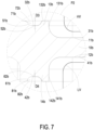
- FIG. 7 is an enlarged view showing the region P2 in FIG. 2 .
- the bearing structure 1b is configured to form a lower half shell.
- the bearing structure 1b includes an insulation carrier 10b, a first conductor layer 31b, a second conductor layer 41b, a first trench 51b and a first insulation material 71b.
- the insulation carrier 10b includes a first surface 11b and a second surface 12b opposite to each other.
- the first conductor layer 31b and the second conductor layer 41b are coated on the first surface 11b and the second surface 12b, respectively.
- a voltage difference is formed between the first conductor layer 31b and the second conductor layer 41b.
- the high-voltage circuit HV is accommodated within the bearing housing 1, and spatially corresponding to the first conductor layer 31b coated on the first surface 11b of the insulation carrier 10b, so that the electric field generated by the high-voltage circuit HV is uniformized through the action of the first conductor layer 31b.
- the second conductor layer 41b coated on the second surface 12b of the insulation carrier 10b of the upper bearing housing 1 is spatially opposite to the low-voltage circuit LV disposed on the outer side of the lower bearing housing.
- the electric field generated by the low-voltage circuit LV outside the lower bearing housing 1 can be uniformized through the action of the second conductor layer 41b of the upper bearing housing 1.
- the voltage difference of the high-voltage circuit HV and the low-voltage circuit LV is formed between the first conductor layer 31b and the second conductor layer 41b.
- the bearing structure 1b includes a first protruding portion 13b, which is protruded from the first surface 11b in a direction (i.e., the Z axial direction) away the second surface 12b.
- the first trench 51b is disposed on the first protruding portion 13b.
- the first conductor layer 31b is coated and disposed on the first surface 11b and a lateral wall 131b and a top surface 132b of the first protruding portion 13b, and extended into the bottom 52b of the first trench 51b.
- the first insulation material 71b covers the outer peripheral edge 32b of the first conductor layer 31b and filled in the first trench 51b.
- the voltage difference formed between the high-voltage circuit HV and the low-voltage circuit LV is ranged from 10 kV to 30 kV.
- the first insulation material 71b is one selected from the group consisting of an epoxy resin, a silicone rubber, a silicone resin and a polyurethane. Moreover, the first insulation material 71b has a dielectric strength greater than 18 kV/mm. Preferably but not exclusively, in the embodiment, the first insulation material 71b is filled into the first trench 51b by fluid dispensing, so that an outer surface 72b of the first insulation material 71b is coplanar with the top surface 132b of the first protruding portion 13b.
- an air electric field strength on the outer surface 72b of the first insulation material 71b is less than 2.0 kV/mm. It avoids the occurrence of corona and partial discharge due to the contact of the air and the outer peripheral edge 32b of the first conductor layer 31b under the high electric field strength.
- the bearing structure 1b includes a second protruding portion 14b, which is protruded from the second surface 12b in a direction (i.e. the reverse Z axial direction) away the first surface 11b.
- the second trench 61b is disposed on the second protruding portion 14b.
- the second conductor layer 41b is coated and disposed on the second surface 12b and a lateral wall 141b and a top surface 142b of the second protruding portion 14b, and extended into the bottom 62b of the second trench 61b.
- the second insulation material 81b is filled into the second trench 61b by fluid dispensing, and the outer surface 82b of the second insulation material 81b and the top surface 142b of the second protruding portion 14b are coplanar.
- the voltage difference formed between the high-voltage circuit HV and the low-voltage circuit LV is ranged from 10 kV to 30 kV.
- the second insulation material 81b is one selected from the group consisting of an epoxy resin, a silicone rubber, a silicone resin and a polyurethane.
- the second insulation material 81b has a dielectric strength greater than 18 kV/mm.
- an air electric field strength on the outer surface 82b of the second insulation material 81b is less than 2.0 kV/mm. It avoids the occurrence of corona and partial discharge due to the contact of the air and the outer peripheral edge 42b of the second conductor layer 41b under the high electric field strength.
- the bearing structures 1a and the bearing structure 1b of the present disclosure are utilized to carry other circuit modules with the high electric field strength generated therefrom.
- the bearing structure 1a and bearing structure 1b designed to seal the outer peripheral edges of the conductor layers through the trenches are not limited to the two half shells of the bearing housing 1.
- the bearing structure 1a and the bearing structure 1b are utilized to form the two symmetrical half shells of the bearing housing 1
- the first insulation materials 71a, 71b and the second insulation materials 81a, 81b are filled into the corresponding first trenches 51a, 51b and the corresponding trenches 61a, 61b by fluid dispensing, respectively. It allows to integrate the formation processes into the manufacturing processes of the bearing housing 1 easily. Moreover, the assembly of the bearing hosing 1 and the power conversion module is not affected.
- first insulation materials 71a, 71b and the second insulation materials 81a, 81b cooperated with the corresponding first trenches 51a, 51b and the corresponding second trenches 61a, 61b are disposed in the bearing housing 1, so that the entire space is not increased. It is not necessary to add an additional space. Thus, the safety specifications and the convenience of the bearing housing for the power conversion module are improved effectively.
- the bearing housing 1 formed by the bearing structure 1a and the bearing structure 1b is advantageous of sandwiching the high-voltage circuit HV in the accommodation space 10 therebetween simply.
- the low-voltage circuit LV is disposed on the outer side of the bearing housing 1. In that, a unit assembly of power conversion module with small volume is achieved.
- the bearing housing 1 formed by the bearing structure 1a and the bearing structure 1b is used to carry the high-low-voltage conversion circuit of the power conversion module in the solid state transformer, it allows to adjust the bearing structure 1a and the bearing structure 1b according to the isolation transformer included in the high-low-voltage conversion circuit.
- a first recessed region (not shown) is formed on the first surface 11a covered by the first conductor layer 31a
- a second recessed region (not shown) is formed on the second surface 12a covered by the second conductor layer 41a
- the first recessed region and the second recessed region are spatially corresponding to each other in position.
- the isolation transformer of the high-low-voltage conversion circuit is disposed correspondingly in the first recessed region and the second recessed region.
- the bearing structure 1b is a symmetrical structure of the bearing structure 1a, and has the same design.
- the present disclosure provides a bearing structure configured to carry a high-low-voltage conversion circuit with high electric field strength.
- the bearing structure is made of an insulation material with a dielectric strength greater than 18 kV/mm.
- a distance is maintained between the outer peripheral edge of the conductor layer and an outer surface of the insulation material and greater than 0.6 mm.
- An air electric field strength on the outer surface of the insulation material is reduced and less than 2.0 kV/mm. It avoids the occurrence of corona and partial discharge due to the contact of the air and the outer peripheral edge of the conductor layer under the high electric field strength.
- the trench and the insulation material are disposed on a peripheral wall formed by the protruding portion, it allows the bearing structure to form an upper half shell or a lower half shell.
- two bearing structures are utilized to form two symmetrical half shells and assembled as a bearing housing.
- the high-voltage circuit is sandwiched between the two symmetrical half shells, and the low-voltage circuit is placed outside the bearing housing, so as to achieve a unit assembly of the power conversion module with small volume. It facilitates to ensure the safety of the solid-state transformer application and enhance the competitiveness of the product.
- the bearing structure having the outer peripheral edge of the conductor layer sealed through the designed trench is allowed to be applied to the bearing housing, which are detached into two symmetrical half shells.
- the insulation material is filled into the trench by fluid dispensing, which is easily integrated into the manufacturing process of the two symmetrical half shells carrying the power conversion module. The entire space is not increased.
- the safety specifications and the convenience of the bearing housing for the power conversion module are improved effectively.
Landscapes
- Engineering & Computer Science (AREA)
- Microelectronics & Electronic Packaging (AREA)
- Casings For Electric Apparatus (AREA)
- Rolling Contact Bearings (AREA)
Abstract
A bearing structure (1a, 1b) for a high-low-voltage conversion circuit is disclosed and includes an insulation carrier (10a, 10b), a first conductor layer (31a, 31b), a second conductor layer (41a, 41b), a first trench (51a, 51b) and a first insulation material (71a, 71b). The first conductor layer (31a, 31b) and the second conductor layer (41a, 41b) are coated on the first surface (11a, 11b) and the second surface (12a, 12b) of the insulation carrier (10a, 10b), respectively. A voltage difference is formed between the first conductor layer (31a, 31b) and the second conductor layer (41a, 41b). The first trench (51a, 51b) is disposed on the first surface (11a, 11b) and surrounds an outer peripheral edge (32a, 32b) of the first conductor layer (31a, 31b). The first conductor layer (31a, 31b) is extended from the first surface (11a, 11b) into the first trench (51a, 51b), and the outer peripheral edge (32a, 32b) of the first conductor layer (31a, 31b) is located at a bottom (52a, 52b) of the first trench (51a, 51b). The first insulation material (71a, 71b) covers the outer peripheral edge (32a, 32b) of the first conductor layer (31a, 31b) and is filled in the first trench (51a, 51b).
Description
- The present disclosure relates to a bearing structure, and more particularly to a bearing structure for a high-low-voltage conversion circuit, so as to avoid the corona and partial discharge due to a high electric field strength on the outer peripheral edge of the conductor.
- With the development of the economy, the demand for electricity has increased sharply. Moreover, the safety requirements for electricity consumption are also getting higher and higher. Taking a common application of medium-voltage solid-state transformers as an example, a plurality of power conversion modules are disposed in a single system cabinet. Each power conversion module needs to be carried on an isolation carrier and be integrated into the system cabinet. Since a high-low voltage conversion circuit is contained in this kind of power conversion module, when the high-voltage circuit and the low-voltage circuit of the high-low conversion circuit are isolated through the isolation carrier, the isolation carrier is further spatially corresponding to a high electric field strength formed due to the voltage difference. Therefore, in order to carry under the action of high electric field strength, the isolation carrier has to avoid the repeated breakdown and extinction phenomenon of partial discharge caused by the structural defects.
- In the conventional power conversion module of the solid-state transformer, the high-voltage circuit and the low-voltage circuit are disposed and corresponding to the conductor layer with a uniform electric field, respectively. However, under the action of high electric field strength, the phenomenon of the corona and partial discharge is generated easily on the outer peripheral edge of the conductor layer.
- Therefore, there is a need of providing a bearing structure configured to carry a high-low-voltage conversion circuit with high electric field strength, wherein the outer peripheral edge of the conductor layer is sealed through the design of the trench, so as to solve the problem of excessive electric field strength generated due to the outer peripheral edge of the conductor layer on the insulation carrier, avoid the occurrence of corona and partial discharge, and obviate the drawbacks encountered by the prior arts.
- An object of the present disclosure is to provide a bearing structure configured to carry a high-low-voltage conversion circuit with high electric field strength. By sealing the outer edge of the conductor layer through the design of the trench, the problem of excessive electric field strength generated due to the outer peripheral edge of the conductor layer on the insulation carrier is solved. Moreover, the occurrence of corona and partial discharge is avoided.
- Another object of the present disclosure is to provide a bearing structure configured to carry and isolate a high-voltage circuit and a low-voltage circuit. The bearing structure is made of an insulation material with a dielectric strength greater than 18 kV/mm. When a high-voltage circuit and a low-voltage circuit with a voltage difference ranged from 10 kV to 30 kV are isolated through the bearing structure, the outer peripheral edge of the conductor layer is sealed by the trench and the insulation material. A distance is maintained between the outer peripheral edge of the conductor layer and an outer surface of the insulation material and greater than 0.6 mm. An air electric field strength on the outer surface of the insulation material is reduced and less than 2.0 kV/mm. It avoids the occurrence of corona and partial discharge due to the contact of the air and the outer peripheral edge of the conductor layer under the high electric field strength. In addition, when the trench and the insulation material are disposed on a peripheral wall formed by the protruding portion, it allows the bearing structure to form an upper half shell or a lower half shell. For example, two bearing structures are utilized to form two symmetrical half shells and assembled as a bearing housing. The high-voltage circuit is sandwiched between the two symmetrical half shells, and the low-voltage circuit is placed outside the bearing housing, so as to achieve a unit assembly of the power conversion module with small volume. It facilitates to ensure the safety of the solid-state transformer application and enhance the competitiveness of the product.
- A further object of the present disclosure is to provide a bearing structure configured to carry a power conversion module with high electric field strength. The bearing structure having the outer peripheral edge of the conductor layer sealed through the designed trench is allowed to be applied to the bearing housing, which are detached into two symmetrical half shells. The insulation material is filled into the trench by fluid dispensing, which is easily integrated into the manufacturing process of the two symmetrical half shells carrying the power conversion module. The entire space is not increased. Thus, the safety specifications and the convenience of the bearing housing for the power conversion module are improved effectively.
- In accordance with an aspect of the present disclosure, a bearing structure is provided and configured to carry a high-low-voltage conversion circuit. The bearing structure includes an insulation carrier, a first conductor layer, a second conductor layer a first trench and a first insulation material. The insulation carrier includes a first surface and a second surface opposite to each other. The first conductor layer and a second conductor layer are coated on the first surface and the second surface, respectively. A voltage difference is formed between the first conductor layer and the second conductor layer. The first trench is disposed on the first surface and surrounds an outer peripheral edge of the first conductor layer. The first conductor layer is extended from the first surface into the first trench, and the outer peripheral edge of the first conductor layer is located at a bottom of the first trench. The first insulation material covers the outer peripheral edge of the first conductor layer and is filled in the first trench.
- The above contents of the present disclosure will become more readily apparent to those ordinarily skilled in the art after reviewing the following detailed description and accompanying drawings, in which:
-
FIG. 1 is a perspective view illustrating a bearing structure utilized to form a bearing housing according to an embodiment of the present disclosure; -
FIG. 2 is a cross-section view illustrating the bearing structure utilized to form the bearing housing and configured to carry a high-low-voltage conversion circuit according to the embodiment of the present disclosure; -
FIG. 3 is a perspective view illustrating the bearing structure utilized to form the bearing housing with the upper half shell and the lower half shell disassembled according to the embodiment of the present disclosure; -
FIGS. 4A and4B are partial exploded views illustrating the upper half shell of the bearing housing formed by the bearing structure according to the embodiment of the present disclosure; -
FIG. 5 is an enlarged view showing the region P1 inFIG. 2 ; -
FIGS. 6A and6B are partial exploded views illustrating the lower half shell of the bearing housing formed by the bearing structure according to the embodiment of the present disclosure; and -
FIG. 7 is an enlarged view showing the region P2 inFIG. 2 . - The present disclosure will now be described more specifically with reference to the following embodiments. It is to be noted that the following descriptions of preferred embodiments of this disclosure are presented herein for purpose of illustration and description only. It is not intended to be exhaustive or to be limited to the precise form disclosed. For example, the formation of a first feature over or on a second feature in the description that follows may include embodiments in which the first and second features are formed in direct contact, and may also include embodiments in which additional features may be formed between the first and second features, such that the first and second features may not be in direct contact. In addition, the present disclosure may repeat reference numerals and/or letters in the various examples. This repetition is for the purpose of simplicity and clarity and does not in itself dictate a relationship between the various embodiments and/or configurations discussed. Further, spatially relative terms, such as "upper," "lower," "top," "bottom" and the like, may be used herein for ease of description to describe one element or feature's relationship to another element(s) or feature(s) as illustrated in the figures. The spatially relative terms are intended to encompass different orientations of the device in use or operation in addition to the orientation depicted in the figures. The apparatus may be otherwise oriented (rotated 90 degrees or at other orientations) and the spatially relative descriptors used herein may likewise be interpreted accordingly. When an element is referred to as being "connected," or "coupled," to another element, it can be directly connected or coupled to the other element or intervening elements may be present. Although the wide numerical ranges and parameters of the present disclosure are approximations, numerical values are set forth in the specific examples as precisely as possible. In addition, although the "first," "second," "third," and the like terms in the claims be used to describe the various elements can be appreciated, these elements should not be limited by these terms, and these elements are described in the respective embodiments are used to express the different reference numerals, these terms are only used to distinguish one element from another element. For example, a first element could be termed a second element, and, similarly, a second element could be termed a first element, without departing from the scope of example embodiments. Besides, "and/or" and the like may be used herein for including any or all combinations of one or more of the associated listed items. Alternatively, the word "about" means within an acceptable standard error of ordinary skill in the art-recognized average. In addition to the operation/working examples, or unless otherwise specifically stated otherwise, in all cases, all of the numerical ranges, amounts, values and percentages, such as the number for the herein disclosed materials, time duration, temperature, operating conditions, the ratio of the amount, and the like, should be understood as the word "about" decorator. Accordingly, unless otherwise indicated, the numerical parameters of the present invention and scope of the appended patent proposed is to follow changes in the desired approximations. At least, the number of significant digits for each numerical parameter should at least be reported and explained by conventional rounding technique is applied. Herein, it can be expressed as a range between from one endpoint to the other or both endpoints. Unless otherwise specified, all ranges disclosed herein are inclusive.
-
FIG. 1 is a perspective view illustrating a bearing structure utilized to form a bearing housing according to an embodiment of the present disclosure.FIG. 2 is a cross-section view illustrating the bearing structure utilized to form the bearing housing and configured to carry a high-low-voltage conversion circuit according to the embodiment of the present disclosure.FIG. 3 is a perspective view illustrating the bearing structure utilized to form the bearing housing with the upper half shell and the lower half shell disassembled according to the embodiment of the present disclosure. In the embodiment, a bearingstructure 1a or abearing structure 1b is configured to carry a high-low-voltage conversion circuit. Preferably but not exclusively, the bearinghousing 1 formed by the bearingstructure 1a and thebearing structure 1b is applied in the field of the solid state transformer (SST), so as to simplify the carrying and assembling procedures of the power conversion module in the solid state transformer. At the same time, it ensures that each unit of the power conversion module meets the safety specifications and avoids the phenomenon of corona and partial discharge caused by the high electric field strength. Certainly, the present disclosure is not limited thereto. Preferably but not exclusively, in the embodiment, the bearingstructure 1a is an upper half shell, the bearingstructure 1b is a lower half shell, and the upper half shell and the lower half shell are symmetrical and assembled with each other to form a bearinghousing 1 having anaccommodation space 10. In an embodiment, the bearinghousing 1 includes afront opening 101 and arear opening 102. Thefront opening 101 and therear opening 102 are in fluid communication with each other through theaccommodation space 10, so as to facilitates the bearinghousing 1 to accommodate a high-voltage circuit HV and provide the functions of ventilation and heat dissipation. Certainly, the present disclosure is not limited thereto. Notably, in case of that the bearinghousing 1 is utilized to carry one unit of the high-low-voltage conversion circuit, the high-voltage circuit HV is sandwiched between the upper half shell of the bearingstructure 1a and the lower half shell of the bearingstructure 1b, and the low-voltage circuit LV is disposed on an outer side of the bearinghousing 1. Preferably but not exclusively, the low-voltage circuit LV is disposed on the top of the upper half shell of the bearingstructure 1a. Certainly, the present disclosure is not limited thereto. In other embodiments, a plurality of units of the power conversion modules are carried on a plurality of bearinghousings 1, respectively, and then stacked with each other. In that, the high-voltage circuit HV accommodated with a bearinghousing 1 and the low-voltage circuit LV disposed outside another bearinghousing 1 have a voltage difference formed between the lower half shell of the bearingstructure 1b. In other words, the bearingstructure 1a and thebearing structure 1b of the present disclosure are not limited to be served as an upper half shell or a lower half shell, and described here firstly. -
FIGS. 4A and4B are partial exploded views illustrating the upper half shell of the bearing housing formed by the bearing structure according to the embodiment of the present disclosure.FIG. 5 is an enlarged view showing the region P1 inFIG. 2 . In the embodiment, the bearingstructure 1a is configured to form an upper half shell. The bearingstructure 1a includes aninsulation carrier 10a, afirst conductor layer 31a, asecond conductor layer 41a, afirst trench 51a and afirst insulation material 71a. Theinsulation carrier 10a includes afirst surface 11a and asecond surface 12a opposite to each other. Preferably but not exclusively, thefirst conductor layer 31a and thesecond conductor layer 41a are the zinc metal coating layers and coated on thefirst surface 11a and thesecond surface 12a, respectively. Moreover, a voltage difference is formed between thefirst conductor layer 31a and thesecond conductor layer 41a. Notably, in the embodiment, the high-voltage circuit HV is disposed on afirst aluminum plate 21 over thefirst conductor layer 31a, and thefirst aluminum plate 21 is spatially corresponding to thefirst conductor layer 31a, so that the electric field generated by the high-voltage circuit HV is uniformized through the action of thefirst conductor layer 31a. Similarly, the low-voltage circuit LV is disposed on asecond aluminum plate 22 over thesecond conductor layer 41a, and thesecond aluminum plate 22 is spatially corresponding to thesecond conductor layer 41a, so that the electric field generated by the low-voltage circuit LV is uniformized through the action of thesecond conductor layer 41a. In other words, the voltage difference of the high-voltage circuit HV and the low-voltage circuit LV is formed between thefirst conductor layer 31a and thesecond conductor layer 41a. Certainly, the types of the high-voltage circuit HV formed on thefirst surface 11a and the low-voltage circuit LV formed on thesecond surface 12a are not limited in the present disclosure. In the embodiment, the voltage difference formed between the high-voltage circuit HV and the low-voltage circuit LV is ranged from 10 kV to 30 kV, but the present disclosure is not limited there. - Notably, in the embodiment, the
first trench 51a is disposed on thefirst surface 11a and surrounds an outerperipheral edge 32a of thefirst conductor layer 31a. Preferably but not exclusively, in the embodiment, thefirst conductor layer 31a is coated on thefirst surface 11a and extended into thefirst trench 51a, so that the outerperipheral edge 32a of thefirst conductor layer 31a is located at a bottom 52a of thefirst trench 51a. In the embodiment, thefirst insulation material 71a covers the outerperipheral edge 32a of thefirst conductor layer 31a and filled in thefirst trench 51a. In the embodiment, the voltage difference formed between the high-voltage circuit HV and the low-voltage circuit LV is ranged from 10 kV to 30 kV Thefirst insulation material 71a is one selected from the group consisting of an epoxy resin, a silicone rubber, a silicone resin and a polyurethane. Moreover, thefirst insulation material 71a has a dielectric strength greater than 18 kV/mm. Preferably but not exclusively, in the embodiment, thefirst insulation material 71a is filled into thefirst trench 51a by fluid dispensing, so that anouter surface 72a of thefirst insulation material 71a is coplanar with the opening of thefirst trench 51a. Thereby, the outerperipheral edge 32a of thefirst conductor layer 31a is sealed through thefirst trench 51a and thefirst insulation material 71a, and a distance D1 is maintained between the outerperipheral edge 32a of thefirst conductor layer 31a and theouter surface 72a of thefirst insulation material 71a and greater than 0.6 mm. According to the result of the partial discharge test, an air electric field strength on theouter surface 72a of thefirst insulation material 71a is less than 2.0 kV/mm. It avoids the occurrence of corona and partial discharge due to the contact of the air and the outerperipheral edge 32a of thefirst conductor layer 31a under the high electric field strength. - In the embodiment, the bearing
structure 1a is constructed on the upper half shell of the supportinghousing 1, and thebearing structure 1a further includes a first protrudingportion 13a, which is protruded from thefirst surface 11a in a direction (i.e., the reverse Z axial direction) away thesecond surface 12a. Thefirst trench 51a is disposed on the first protrudingportion 13a. Thefirst conductor layer 31a is coated and disposed on thefirst surface 11a and alateral wall 131a and atop surface 132a of the first protrudingportion 13a, and extended into the bottom 52a of thefirst trench 51a. Since thefirst trench 51a is disposed on the first protrudingportion 13a, when thefirst insulation material 71a is filled into thefirst trench 51a by fluid dispensing, the lateral-wall structure of the first protrudingportion 13a is helpful of performing the fluid dispensing, and preventing the fluid that is not solidified to form thefirst insulation material 71a from overflowing everywhere. Preferably but not exclusively, in an embodiment, theouter surface 72a of thefirst insulation material 71a and thetop surface 132a of the first protrudingportion 13a are coplanar. Certainly, the present disclosure is not limited thereto. - Moreover, in the embodiment, the bearing
structure 1a further includes asecond trench 61a and asecond insulation material 81a. Thesecond trench 61a is disposed on thesecond surface 12a and surrounds an outerperipheral edge 42a of thesecond conductor layer 41a. Preferably but not exclusively, in the embodiment, thesecond conductor layer 41a is coated on thesecond surface 12a and extended into thesecond trench 61a, so that the outerperipheral edge 42a of thesecond conductor layer 41a is located at a bottom 62a of thesecond trench 61a. In the embodiment, thesecond insulation material 81a is filled in thesecond trench 61a, and covers the outerperipheral edge 42a of thesecond conductor layer 41a. Similarly, the bearingstructure 1a further includes a second protrudingportion 14a, which is protruded from thesecond surface 12a in a direction (i.e. the Z axial direction) away thefirst surface 11a. Thesecond trench 61a is disposed on the second protrudingportion 14a. Thesecond conductor layer 41a is coated and disposed on thesecond surface 12a and alateral wall 141a and atop surface 142a of the second protrudingportion 14a, and extended into the bottom 62a of thesecond trench 61a. Since thesecond trench 61a is disposed on the second protrudingportion 14a, when thesecond insulation material 81a is filled into thesecond trench 61a by fluid dispensing, the lateral-wall structure of the second protrudingportion 14a is helpful of performing the fluid dispensing, and preventing the fluid that is not solidified to form thesecond insulation material 81a from overflowing everywhere. Preferably but not exclusively, in an embodiment, theouter surface 82a of thesecond insulation material 81a and thetop surface 142a of the second protrudingportion 14a are coplanar. Preferably but not exclusively, in the embodiment, the voltage difference formed between the high-voltage circuit HV and the low-voltage circuit LV is ranged from 10 kV to 30 kV. Thesecond insulation material 81a is one selected from the group consisting of an epoxy resin, a silicone rubber, a silicone resin and a polyurethane. Moreover, thesecond insulation material 81a has a dielectric strength greater than 18 kV/mm. Since the outerperipheral edge 42a of thesecond conductor layer 41a is sealed through thesecond trench 61a and thesecond insulation material 81a, and a distance D2 is maintained between the outerperipheral edge 42a of thesecond conductor layer 41a and theouter surface 82a of thesecond insulation material 81a and greater than 0.6 mm. According to the result of the partial discharge test, an air electric field strength on theouter surface 82a of thesecond insulation material 81a is less than 2.0 kV/mm. It avoids the occurrence of corona and partial discharge due to the contact of the air and the outerperipheral edge 42a of thesecond conductor layer 41a under the high electric field strength. - Notably, in the embodiment, the heights of the first protruding
portion 13a and/or the second protrudingportion 14a are adjustable according to the practical requirements. In other embodiments, the first protrudingportion 13a and/or the second protrudingportion 14a are omitted. In an embodiment, thefirst trench 51a is recessed directly from thefirst surface 11a toward thesecond surface 12a (i.e. in the Z axial direction). Moreover, thefirst conductor layer 31a is coated and disposed on thefirst surface 11a, and extended directly from thefirst surface 11a to the bottom 52a of thefirst trench 51a. In that, thefirst insulation material 71a covers the outerperipheral edge 32a of thefirst conductor layer 31a, and the outerperipheral edge 32a of thefirst conductor layer 31a is sealed. Preferably but not exclusively, in an embodiment, theouter surface 72a of thefirst insulation material 71a is substantially coplanar with thefirst surface 11a. In another embodiment, thesecond trench 61a is recessed directly from thesecond surface 12a toward thefirst surface 11a (i.e. in the reverse Z axial direction). Moreover, thesecond conductor layer 41a is coated and disposed on thesecond surface 12a, and extended directly from thesecond surface 12a to the bottom 62a of thesecond trench 61a. In that, thesecond insulation material 81a covers the outerperipheral edge 42a of thesecond conductor layer 41a, and the outerperipheral edge 42a of thesecond conductor layer 41a is sealed. Preferably but not exclusively, in an embodiment, theouter surface 82a of thesecond insulation material 81a is substantially coplanar with thesecond surface 12a. Certainly, the present disclosure is not limited thereto, and not redundantly described herein. -
FIGS. 6A and6B are partial exploded views illustrating the lower half shell of the bearing housing formed by the bearing structure according to the embodiment of the present disclosure.FIG. 7 is an enlarged view showing the region P2 inFIG. 2 . In the embodiment, the bearingstructure 1b is configured to form a lower half shell. The bearingstructure 1b includes aninsulation carrier 10b, afirst conductor layer 31b, asecond conductor layer 41b, afirst trench 51b and afirst insulation material 71b. Theinsulation carrier 10b includes afirst surface 11b and asecond surface 12b opposite to each other. Preferably but not exclusively, thefirst conductor layer 31b and thesecond conductor layer 41b are coated on thefirst surface 11b and thesecond surface 12b, respectively. Moreover, a voltage difference is formed between thefirst conductor layer 31b and thesecond conductor layer 41b. Notably, in the embodiment, the high-voltage circuit HV is accommodated within the bearinghousing 1, and spatially corresponding to thefirst conductor layer 31b coated on thefirst surface 11b of theinsulation carrier 10b, so that the electric field generated by the high-voltage circuit HV is uniformized through the action of thefirst conductor layer 31b. On the other hand, when the twobearing housings 1 with the power conversion modules carried thereon are stacked with each other, thesecond conductor layer 41b coated on thesecond surface 12b of theinsulation carrier 10b of theupper bearing housing 1 is spatially opposite to the low-voltage circuit LV disposed on the outer side of the lower bearing housing. 1, so that the electric field generated by the low-voltage circuit LV outside thelower bearing housing 1 can be uniformized through the action of thesecond conductor layer 41b of theupper bearing housing 1. In other words, the voltage difference of the high-voltage circuit HV and the low-voltage circuit LV is formed between thefirst conductor layer 31b and thesecond conductor layer 41b. - In the embodiment, the bearing
structure 1b includes a first protrudingportion 13b, which is protruded from thefirst surface 11b in a direction (i.e., the Z axial direction) away thesecond surface 12b. Thefirst trench 51b is disposed on the first protrudingportion 13b. Thefirst conductor layer 31b is coated and disposed on thefirst surface 11b and alateral wall 131b and atop surface 132b of the first protrudingportion 13b, and extended into the bottom 52b of thefirst trench 51b. In the embodiment, thefirst insulation material 71b covers the outerperipheral edge 32b of thefirst conductor layer 31b and filled in thefirst trench 51b. In the embodiment, the voltage difference formed between the high-voltage circuit HV and the low-voltage circuit LV is ranged from 10 kV to 30 kV. Thefirst insulation material 71b is one selected from the group consisting of an epoxy resin, a silicone rubber, a silicone resin and a polyurethane. Moreover, thefirst insulation material 71b has a dielectric strength greater than 18 kV/mm. Preferably but not exclusively, in the embodiment, thefirst insulation material 71b is filled into thefirst trench 51b by fluid dispensing, so that anouter surface 72b of thefirst insulation material 71b is coplanar with thetop surface 132b of the first protrudingportion 13b. Thereby, the outerperipheral edge 32b of thefirst conductor layer 31b is sealed through thefirst trench 51b and thefirst insulation material 71b, and a distance D3 is maintained between the outerperipheral edge 32b of thefirst conductor layer 31b and theouter surface 72b of thefirst insulation material 71b and greater than 0.6 mm. According to the result of the partial discharge test, an air electric field strength on theouter surface 72b of thefirst insulation material 71b is less than 2.0 kV/mm. It avoids the occurrence of corona and partial discharge due to the contact of the air and the outerperipheral edge 32b of thefirst conductor layer 31b under the high electric field strength. - Similarly, in the embodiment, the bearing
structure 1b includes a second protrudingportion 14b, which is protruded from thesecond surface 12b in a direction (i.e. the reverse Z axial direction) away thefirst surface 11b. Thesecond trench 61b is disposed on the second protrudingportion 14b. Thesecond conductor layer 41b is coated and disposed on thesecond surface 12b and alateral wall 141b and atop surface 142b of the second protrudingportion 14b, and extended into the bottom 62b of thesecond trench 61b. Thesecond insulation material 81b is filled into thesecond trench 61b by fluid dispensing, and theouter surface 82b of thesecond insulation material 81b and thetop surface 142b of the second protrudingportion 14b are coplanar. Preferably but not exclusively, in the embodiment, the voltage difference formed between the high-voltage circuit HV and the low-voltage circuit LV is ranged from 10 kV to 30 kV. Thesecond insulation material 81b is one selected from the group consisting of an epoxy resin, a silicone rubber, a silicone resin and a polyurethane. Moreover, thesecond insulation material 81b has a dielectric strength greater than 18 kV/mm. Since the outerperipheral edge 42b of thesecond conductor layer 41b is sealed through thesecond trench 61b and thesecond insulation material 81b, and a distance D4 is maintained between the outerperipheral edge 42b of thesecond conductor layer 41b and theouter surface 82b of thesecond insulation material 81b and greater than 0.6 mm. According to the result of the partial discharge test, an air electric field strength on theouter surface 82b of thesecond insulation material 81b is less than 2.0 kV/mm. It avoids the occurrence of corona and partial discharge due to the contact of the air and the outerperipheral edge 42b of thesecond conductor layer 41b under the high electric field strength. - In other embodiment, the bearing
structures 1a and thebearing structure 1b of the present disclosure are utilized to carry other circuit modules with the high electric field strength generated therefrom. By sealing the outer edge of the conductor layer through the design of the trench, the problem of excessive electric field strength generated due to the outer peripheral edge of the conductor layer on the insulation carrier is solved, and the occurrence of corona and partial discharge is avoided. Certainly, the bearingstructure 1a andbearing structure 1b designed to seal the outer peripheral edges of the conductor layers through the trenches are not limited to the two half shells of the bearinghousing 1. However, in the case of that the bearingstructure 1a and thebearing structure 1b are utilized to form the two symmetrical half shells of the bearinghousing 1, thefirst insulation materials second insulation materials first trenches corresponding trenches housing 1 easily. Moreover, the assembly of the bearing hosing 1 and the power conversion module is not affected. In addition, thefirst insulation materials second insulation materials first trenches second trenches housing 1, so that the entire space is not increased. It is not necessary to add an additional space. Thus, the safety specifications and the convenience of the bearing housing for the power conversion module are improved effectively. The bearinghousing 1 formed by the bearingstructure 1a and thebearing structure 1b is advantageous of sandwiching the high-voltage circuit HV in theaccommodation space 10 therebetween simply. Furthermore, the low-voltage circuit LV is disposed on the outer side of the bearinghousing 1. In that, a unit assembly of power conversion module with small volume is achieved. It facilitates to ensure the safety of the solid-state transformer application and enhance the competitiveness of the product. On the other hand, in case of that the bearinghousing 1 formed by the bearingstructure 1a and thebearing structure 1b is used to carry the high-low-voltage conversion circuit of the power conversion module in the solid state transformer, it allows to adjust thebearing structure 1a and thebearing structure 1b according to the isolation transformer included in the high-low-voltage conversion circuit. Referring toFIGS. 1 to 3 and taking the bearingstructure 1a as an example, in an embodiment, a first recessed region (not shown) is formed on thefirst surface 11a covered by thefirst conductor layer 31a, a second recessed region (not shown) is formed on thesecond surface 12a covered by thesecond conductor layer 41a, and the first recessed region and the second recessed region are spatially corresponding to each other in position. In that, the isolation transformer of the high-low-voltage conversion circuit is disposed correspondingly in the first recessed region and the second recessed region. Similarly, the bearingstructure 1b is a symmetrical structure of the bearingstructure 1a, and has the same design. However, it is not an essential feature of the present disclosure, and the effects of sealing outer peripheral edges of thefirst conductor layers - In summary, the present disclosure provides a bearing structure configured to carry a high-low-voltage conversion circuit with high electric field strength. By sealing the outer edge of the conductor layer through the design of the trench, the problem of excessive electric field strength generated due to the outer peripheral edge of the conductor layer on the insulation carrier is solved. Moreover, the occurrence of corona and partial discharge is avoided. The bearing structure is made of an insulation material with a dielectric strength greater than 18 kV/mm. When a high-voltage circuit and a low-voltage circuit with a voltage difference ranged from 10 kV to 30 kV are isolated through the bearing structure, the outer peripheral edge of the conductor layer is sealed by the trench and the insulation material. In that, a distance is maintained between the outer peripheral edge of the conductor layer and an outer surface of the insulation material and greater than 0.6 mm. An air electric field strength on the outer surface of the insulation material is reduced and less than 2.0 kV/mm. It avoids the occurrence of corona and partial discharge due to the contact of the air and the outer peripheral edge of the conductor layer under the high electric field strength. In addition, when the trench and the insulation material are disposed on a peripheral wall formed by the protruding portion, it allows the bearing structure to form an upper half shell or a lower half shell. For example, two bearing structures are utilized to form two symmetrical half shells and assembled as a bearing housing. The high-voltage circuit is sandwiched between the two symmetrical half shells, and the low-voltage circuit is placed outside the bearing housing, so as to achieve a unit assembly of the power conversion module with small volume. It facilitates to ensure the safety of the solid-state transformer application and enhance the competitiveness of the product. On the other hand, the bearing structure having the outer peripheral edge of the conductor layer sealed through the designed trench is allowed to be applied to the bearing housing, which are detached into two symmetrical half shells. The insulation material is filled into the trench by fluid dispensing, which is easily integrated into the manufacturing process of the two symmetrical half shells carrying the power conversion module. The entire space is not increased. Thus, the safety specifications and the convenience of the bearing housing for the power conversion module are improved effectively.
Claims (15)
- A bearing structure (1a, 1b) configured to carry a high-low-voltage conversion circuit, and characterized by comprising:an insulation carrier (10a, 10b) comprising a first surface (11a, 11b) and a second surface (12a, 12b) opposite to each other;a first conductor layer (31a, 31b) and a second conductor layer (41a, 41b) coated on the first surface (11a, 11b) and the second surface (12a, 12b), respectively, wherein a voltage difference is formed between the first conductor layer (31a, 31b) and the second conductor layer (41a, 41b);a first trench (51a, 51b) disposed on the first surface (11a, 11b) and surrounding an outer peripheral edge (32a, 32b) of the first conductor layer (31a, 31b), wherein the first conductor layer (31a, 31b) is extended from the first surface (11a, 11b) into the first trench (51a, 51b), and the outer peripheral edge (32a, 32b) of the first conductor layer (31a, 31b) is located at a bottom (52a, 52b) of the first trench (51a, 51b); anda first insulation material (71a, 71b) covering the outer peripheral edge (32a, 32b) of the first conductor layer (31a, 31b) and filled in the first trench (51a, 51b).
- The bearing structure (1a, 1b) according to claim 1, wherein the high-low-voltage conversion circuit is a power conversion module of a solid-state transformer.
- The bearing structure (1a, 1b) according to claim 1, wherein the high-low-voltage conversion circuit comprises a high-voltage circuit (HV) and a low-voltage circuit (LV), wherein the high-voltage circuit (HV) is disposed on the first surface (11a, 11b) and spatially corresponding to the first conductor layer (31a, 31b), and the low-voltage circuit (LV) is disposed on the second surface (12a, 12b) and spatially corresponding to the first conductor layer (31a, 31b), so that the voltage difference is formed between the first conductor layer (31a, 31) and the second conductor layer (41a, 41b).
- The bearing structure (1a, 1b) according to claim 3, wherein a half shell is formed by the bearing structure (1a, 1b), and two of the half shells are assembled to form a bearing housing (1), wherein the high-voltage circuit (HV) is accommodated within the bearing housing (1), and the low-voltage circuit (LV) is disposed on an outer side of the bearing housing (1).
- The bearing structure (1a, 1b) according to claim 3, wherein the voltage difference formed between the first conductor layer (31a, 31b) and the second conductor layer (41a, 41b) is ranged from 10 kV to 30 kV.
- The bearing structure (1a, 1b) according to claim 1, wherein a distance (D1, D3) is maintained between the outer peripheral edge (32a, 32b) of the first conductor layer (31a, 31b) and an outer surface (72a, 72b) of the first insulation material (71a, 71b) and greater than 0.6 mm, wherein an air electric field strength on an outer surface (72a, 72b) of the first insulation material (71a, 71b) is less than 2.0 kV/mm.
- The bearing structure (1a, 1b) according to claim 1, wherein the first insulation material (71a, 71b) is one selected from the group consisting of an epoxy resin, a silicone rubber, a silicone resin and a polyurethane, wherein the first insulation material (71a, 71b) has a dielectric strength greater than 18 kV/mm, wherein the first insulation material (71a, 71b) is filled into the first trench (51a, 51b) by fluid dispensing.
- The bearing structure (1a, 1b) according to claim 1, further comprising a first protruding portion (13a ,13b) protruded from the first surface (11a, 11b) in a direction away the second surface (12a, 12b), wherein the first trench (51a, 51b)is disposed on the first protruding portion (13a, 13b), wherein the first conductor layer (31a, 31b) is disposed on the first surface (11a, 11b) and a lateral wall (131a, 131b) and a top surface (132a, 132b) of the first protruding portion (13a, 13b), and extended into the first trench (51a, 51b).
- The bearing structure (1a, 1b) according to claim 8, wherein an outer surface (72a, 72b) of the first insulation material (71a, 71b) and the top surface (132a, 132b) of the first protruding portion (13a, 13b) are coplanar.
- The bearing structure (1a, 1b) according to claim 1, further comprising:a second trench (61a, 61b) disposed on the second surface (12a, 12b) and surrounding an outer peripheral edge (42a, 42b) of the second conductor layer (41a, 41b), wherein the second conductor layer (41a, 41b) is extended from the second surface (12a, 12b) into the second trench (61a, 61b), and the outer peripheral edge (42a, 42b) of the second conductor layer (41a, 41b) is located at a bottom (62a, 62b) of the second trench (61a, 61b); anda second insulation material (81a, 81b) filled in the second trench (61a, 61b) and covering the outer peripheral edge (42a, 42b) of the second conductor layer (41a, 41b).
- The bearing structure (1a, 1b) according to claim 10, wherein a distance (D2, D4) is maintained between the outer peripheral edge (42a, 42b) of the second conductor layer (41a, 41b) and an outer surface (82a, 82b) of the second insulation material (81a, 81b) and greater than 0.6 mm, wherein an air electric field strength on an outer surface (82a, 82b) of the second insulation material (81a, 81b) is less than 2.0 kV/mm.
- The bearing structure (1a, 1b) according to claim 10, wherein the second insulation material (81a, 81b) is one selected from the group consisting of an epoxy resin, a silicone rubber, a silicone resin and a polyurethane, wherein the second insulation material (81a, 81b) has a dielectric strength greater than 18 kV/mm, wherein the second insulation material (81a, 81b) is filled into the second trench (61a, 61b) by fluid dispensing.
- The bearing structure (1a, 1b) according to claim 10, further comprising a second protruding portion (14a, 14b)) protruded from the second surface (12a, 12b) in a direction away the first surface (11a, 11b), wherein the second trench (61a, 61b) is disposed on the second protruding portion (14a, 14b), wherein the second conductor layer (41a, 41b) is disposed on the second surface (12a, 12b) and a lateral wall (141a, 141b) and a top surface (142a, 142b) of the second protruding portion (14a, 14b), and extended into the second trench (61a, 61b).
- The bearing structure (1a, 1b) according to claim 13, wherein an outer surface (82a, 82b) of the second insulation material (81a, 81b) and the top surface (142a, 142b) of the second protruding portion (14a, 14b) are coplanar.
- The bearing structure (1a, 1b) according to claim 1, wherein a first recessed region is formed on the first surface (11a, 11b) covered by the first conductor layer (31a, 31b), a second recessed region is formed on the second surface (12a, 12b) covered by the second conductor layer (41a, 41b), and the first recessed region and the second recessed region are spatially corresponding to each other in position, wherein the high-low-voltage conversion circuit comprises an isolation transformer disposed correspondingly in the first recessed region and the second recessed region.
Applications Claiming Priority (1)
| Application Number | Priority Date | Filing Date | Title |
|---|---|---|---|
| CN202210509627.4A CN117098348A (en) | 2022-05-11 | 2022-05-11 | Load-bearing structure of high and low voltage conversion circuit |
Publications (1)
| Publication Number | Publication Date |
|---|---|
| EP4276858A1 true EP4276858A1 (en) | 2023-11-15 |
Family
ID=82932557
Family Applications (1)
| Application Number | Title | Priority Date | Filing Date |
|---|---|---|---|
| EP22186888.8A Pending EP4276858A1 (en) | 2022-05-11 | 2022-07-26 | Bearing structure for high-low-voltage conversion circuit |
Country Status (3)
| Country | Link |
|---|---|
| US (1) | US12096582B2 (en) |
| EP (1) | EP4276858A1 (en) |
| CN (1) | CN117098348A (en) |
Citations (4)
| Publication number | Priority date | Publication date | Assignee | Title |
|---|---|---|---|---|
| WO2014192817A1 (en) * | 2013-05-28 | 2014-12-04 | 矢崎総業株式会社 | Power supply coil unit |
| US20180153046A1 (en) * | 2016-11-29 | 2018-05-31 | Delta Electronics (Shanghai) Co., Ltd. | Apparatus for installing high and low voltage conversion circuit, high and low voltage conversion system and power source |
| US20190207529A1 (en) * | 2016-08-09 | 2019-07-04 | Raytheon Company | High voltage high frequency power converter |
| CN114465445A (en) * | 2020-11-06 | 2022-05-10 | 台达电子企业管理(上海)有限公司 | Power module and power conversion device |
Family Cites Families (9)
| Publication number | Priority date | Publication date | Assignee | Title |
|---|---|---|---|---|
| EP0262482B1 (en) * | 1986-09-30 | 1991-05-29 | Siemens Aktiengesellschaft | Housing for receiving card frames |
| US6320762B1 (en) * | 1999-04-09 | 2001-11-20 | Shiaw-Jong S. Chen | Fixed conductive pin for printed wiring substrate electronics case and method of manufacture therefor |
| DE10113912B4 (en) * | 2001-03-21 | 2006-09-28 | Siemens Ag | Electronic device |
| US6885277B2 (en) * | 2002-09-12 | 2005-04-26 | Kung-Chao Tung | Externally adjustable impedance transformer |
| DE102004061818A1 (en) * | 2004-12-22 | 2006-07-06 | Robert Bosch Gmbh | control module |
| JP2008098201A (en) * | 2006-10-05 | 2008-04-24 | Denso Corp | Semiconductor device |
| JP5117917B2 (en) * | 2008-04-21 | 2013-01-16 | デクセリアルズ株式会社 | Protective element and manufacturing method thereof |
| CN114501915B (en) * | 2020-10-27 | 2024-09-03 | 北京小米移动软件有限公司 | Electronic devices |
| JP7151922B1 (en) * | 2022-04-25 | 2022-10-12 | 富士電機株式会社 | power converter |
-
2022
- 2022-05-11 CN CN202210509627.4A patent/CN117098348A/en active Pending
- 2022-07-26 EP EP22186888.8A patent/EP4276858A1/en active Pending
- 2022-07-27 US US17/875,130 patent/US12096582B2/en active Active
Patent Citations (4)
| Publication number | Priority date | Publication date | Assignee | Title |
|---|---|---|---|---|
| WO2014192817A1 (en) * | 2013-05-28 | 2014-12-04 | 矢崎総業株式会社 | Power supply coil unit |
| US20190207529A1 (en) * | 2016-08-09 | 2019-07-04 | Raytheon Company | High voltage high frequency power converter |
| US20180153046A1 (en) * | 2016-11-29 | 2018-05-31 | Delta Electronics (Shanghai) Co., Ltd. | Apparatus for installing high and low voltage conversion circuit, high and low voltage conversion system and power source |
| CN114465445A (en) * | 2020-11-06 | 2022-05-10 | 台达电子企业管理(上海)有限公司 | Power module and power conversion device |
Also Published As
| Publication number | Publication date |
|---|---|
| US20230371194A1 (en) | 2023-11-16 |
| CN117098348A (en) | 2023-11-21 |
| US12096582B2 (en) | 2024-09-17 |
Similar Documents
| Publication | Publication Date | Title |
|---|---|---|
| US10529499B2 (en) | Electricity storage unit | |
| US20140268578A1 (en) | Electronic Device With Heat Dissipating Electromagnetic Interference Shielding Structures | |
| US11126231B2 (en) | Display device and grounding device thereof | |
| EP3333931B1 (en) | Secondary battery | |
| US20220407433A1 (en) | Power module of isolated converter | |
| EP4064428A1 (en) | Battery cell, feed-through assembly and electronic device | |
| KR102401422B1 (en) | Plasma Etching Chamber and Plasma Etching Method | |
| US12096582B2 (en) | Bearing structure for high-low-voltage conversion circuit | |
| JP7798914B2 (en) | Battery cells and electrical equipment | |
| US11189431B2 (en) | Low profile wet electrolytic tantalum capacitor | |
| CN118678747A (en) | Display panel, preparation method thereof and display device | |
| JP2014170882A (en) | Capacitor | |
| US20210351429A1 (en) | Secondary Battery Including Electronde Lead And Method For Manufacturing The Same | |
| US20170338450A1 (en) | Secondary electrochemical battery sealing body with charging indicator | |
| US20140050968A1 (en) | Battery pack | |
| TWI813281B (en) | Bearing structure for high-low-voltage conversion circuit | |
| US20230231280A1 (en) | Battery unit and feedthrough assembly | |
| US10873064B2 (en) | Energy storage apparatus | |
| US8193467B2 (en) | Insulator with disc-shaped carrier element | |
| CN206099905U (en) | Microwave four -channel amplifier module | |
| KR101936800B1 (en) | Energy storage apparatus integrated with case | |
| CN102436930B (en) | Combined capacitor | |
| CN223583288U (en) | Adapter boards and electrical equipment | |
| CN213214108U (en) | Isolation structure | |
| CN112687994A (en) | Button cell |
Legal Events
| Date | Code | Title | Description |
|---|---|---|---|
| PUAI | Public reference made under article 153(3) epc to a published international application that has entered the european phase |
Free format text: ORIGINAL CODE: 0009012 |
|
| STAA | Information on the status of an ep patent application or granted ep patent |
Free format text: STATUS: REQUEST FOR EXAMINATION WAS MADE |
|
| 17P | Request for examination filed |
Effective date: 20231004 |
|
| AK | Designated contracting states |
Kind code of ref document: A1 Designated state(s): AL AT BE BG CH CY CZ DE DK EE ES FI FR GB GR HR HU IE IS IT LI LT LU LV MC MK MT NL NO PL PT RO RS SE SI SK SM TR |