EP4276832A1 - Address refresh circuit, method, memory, and electronic device - Google Patents
Address refresh circuit, method, memory, and electronic device Download PDFInfo
- Publication number
- EP4276832A1 EP4276832A1 EP22902593.7A EP22902593A EP4276832A1 EP 4276832 A1 EP4276832 A1 EP 4276832A1 EP 22902593 A EP22902593 A EP 22902593A EP 4276832 A1 EP4276832 A1 EP 4276832A1
- Authority
- EP
- European Patent Office
- Prior art keywords
- signal
- address signal
- level
- refresh
- address
- Prior art date
- Legal status (The legal status is an assumption and is not a legal conclusion. Google has not performed a legal analysis and makes no representation as to the accuracy of the status listed.)
- Withdrawn
Links
Images





Classifications
-
- G—PHYSICS
- G11—INFORMATION STORAGE
- G11C—STATIC STORES
- G11C11/00—Digital stores characterised by the use of particular electric or magnetic storage elements; Storage elements therefor
- G11C11/21—Digital stores characterised by the use of particular electric or magnetic storage elements; Storage elements therefor using electric elements
- G11C11/34—Digital stores characterised by the use of particular electric or magnetic storage elements; Storage elements therefor using electric elements using semiconductor devices
- G11C11/40—Digital stores characterised by the use of particular electric or magnetic storage elements; Storage elements therefor using electric elements using semiconductor devices using transistors
- G11C11/401—Digital stores characterised by the use of particular electric or magnetic storage elements; Storage elements therefor using electric elements using semiconductor devices using transistors forming cells needing refreshing or charge regeneration, i.e. dynamic cells
- G11C11/406—Management or control of the refreshing or charge-regeneration cycles
-
- G—PHYSICS
- G11—INFORMATION STORAGE
- G11C—STATIC STORES
- G11C11/00—Digital stores characterised by the use of particular electric or magnetic storage elements; Storage elements therefor
- G11C11/21—Digital stores characterised by the use of particular electric or magnetic storage elements; Storage elements therefor using electric elements
- G11C11/34—Digital stores characterised by the use of particular electric or magnetic storage elements; Storage elements therefor using electric elements using semiconductor devices
- G11C11/40—Digital stores characterised by the use of particular electric or magnetic storage elements; Storage elements therefor using electric elements using semiconductor devices using transistors
- G11C11/401—Digital stores characterised by the use of particular electric or magnetic storage elements; Storage elements therefor using electric elements using semiconductor devices using transistors forming cells needing refreshing or charge regeneration, i.e. dynamic cells
- G11C11/4063—Auxiliary circuits, e.g. for addressing, decoding, driving, writing, sensing or timing
- G11C11/407—Auxiliary circuits, e.g. for addressing, decoding, driving, writing, sensing or timing for memory cells of the field-effect type
- G11C11/408—Address circuits
- G11C11/4087—Address decoders, e.g. bit - or word line decoders; Multiple line decoders
-
- G—PHYSICS
- G06—COMPUTING OR CALCULATING; COUNTING
- G06F—ELECTRIC DIGITAL DATA PROCESSING
- G06F13/00—Interconnection of, or transfer of information or other signals between, memories, input/output devices or central processing units
- G06F13/14—Handling requests for interconnection or transfer
-
- G—PHYSICS
- G11—INFORMATION STORAGE
- G11C—STATIC STORES
- G11C11/00—Digital stores characterised by the use of particular electric or magnetic storage elements; Storage elements therefor
- G11C11/21—Digital stores characterised by the use of particular electric or magnetic storage elements; Storage elements therefor using electric elements
- G11C11/34—Digital stores characterised by the use of particular electric or magnetic storage elements; Storage elements therefor using electric elements using semiconductor devices
- G11C11/40—Digital stores characterised by the use of particular electric or magnetic storage elements; Storage elements therefor using electric elements using semiconductor devices using transistors
- G11C11/401—Digital stores characterised by the use of particular electric or magnetic storage elements; Storage elements therefor using electric elements using semiconductor devices using transistors forming cells needing refreshing or charge regeneration, i.e. dynamic cells
-
- G—PHYSICS
- G11—INFORMATION STORAGE
- G11C—STATIC STORES
- G11C11/00—Digital stores characterised by the use of particular electric or magnetic storage elements; Storage elements therefor
- G11C11/21—Digital stores characterised by the use of particular electric or magnetic storage elements; Storage elements therefor using electric elements
- G11C11/34—Digital stores characterised by the use of particular electric or magnetic storage elements; Storage elements therefor using electric elements using semiconductor devices
- G11C11/40—Digital stores characterised by the use of particular electric or magnetic storage elements; Storage elements therefor using electric elements using semiconductor devices using transistors
- G11C11/401—Digital stores characterised by the use of particular electric or magnetic storage elements; Storage elements therefor using electric elements using semiconductor devices using transistors forming cells needing refreshing or charge regeneration, i.e. dynamic cells
- G11C11/406—Management or control of the refreshing or charge-regeneration cycles
- G11C11/40603—Arbitration, priority and concurrent access to memory cells for read/write or refresh operations
-
- G—PHYSICS
- G11—INFORMATION STORAGE
- G11C—STATIC STORES
- G11C11/00—Digital stores characterised by the use of particular electric or magnetic storage elements; Storage elements therefor
- G11C11/21—Digital stores characterised by the use of particular electric or magnetic storage elements; Storage elements therefor using electric elements
- G11C11/34—Digital stores characterised by the use of particular electric or magnetic storage elements; Storage elements therefor using electric elements using semiconductor devices
- G11C11/40—Digital stores characterised by the use of particular electric or magnetic storage elements; Storage elements therefor using electric elements using semiconductor devices using transistors
- G11C11/401—Digital stores characterised by the use of particular electric or magnetic storage elements; Storage elements therefor using electric elements using semiconductor devices using transistors forming cells needing refreshing or charge regeneration, i.e. dynamic cells
- G11C11/4063—Auxiliary circuits, e.g. for addressing, decoding, driving, writing, sensing or timing
-
- G—PHYSICS
- G11—INFORMATION STORAGE
- G11C—STATIC STORES
- G11C29/00—Checking stores for correct operation ; Subsequent repair; Testing stores during standby or offline operation
- G11C29/70—Masking faults in memories by using spares or by reconfiguring
- G11C29/76—Masking faults in memories by using spares or by reconfiguring using address translation or modifications
-
- G—PHYSICS
- G11—INFORMATION STORAGE
- G11C—STATIC STORES
- G11C29/00—Checking stores for correct operation ; Subsequent repair; Testing stores during standby or offline operation
- G11C29/70—Masking faults in memories by using spares or by reconfiguring
- G11C29/78—Masking faults in memories by using spares or by reconfiguring using programmable devices
- G11C29/781—Masking faults in memories by using spares or by reconfiguring using programmable devices combined in a redundant decoder
-
- G—PHYSICS
- G11—INFORMATION STORAGE
- G11C—STATIC STORES
- G11C8/00—Arrangements for selecting an address in a digital store
- G11C8/18—Address timing or clocking circuits; Address control signal generation or management, e.g. for row address strobe [RAS] or column address strobe [CAS] signals
-
- Y—GENERAL TAGGING OF NEW TECHNOLOGICAL DEVELOPMENTS; GENERAL TAGGING OF CROSS-SECTIONAL TECHNOLOGIES SPANNING OVER SEVERAL SECTIONS OF THE IPC; TECHNICAL SUBJECTS COVERED BY FORMER USPC CROSS-REFERENCE ART COLLECTIONS [XRACs] AND DIGESTS
- Y02—TECHNOLOGIES OR APPLICATIONS FOR MITIGATION OR ADAPTATION AGAINST CLIMATE CHANGE
- Y02D—CLIMATE CHANGE MITIGATION TECHNOLOGIES IN INFORMATION AND COMMUNICATION TECHNOLOGIES [ICT], I.E. INFORMATION AND COMMUNICATION TECHNOLOGIES AIMING AT THE REDUCTION OF THEIR OWN ENERGY USE
- Y02D10/00—Energy efficient computing, e.g. low power processors, power management or thermal management
Definitions
- the disclosure relates to the field of integrated circuits, and in particular to an address refresh circuit and method, a memory, and an electronic device.
- the Dynamic Random Access Memory is a volatile semiconductor memory device that stores data by using charges stored in capacitors. Since the charges stored in the capacitors may leak in various ways over time, the DRAM has a characteristic of limited data retention. In order to solve the limited data retention, the DRAM usually needs to be refreshed periodically based on the data stored in the DRAM, to charge or discharge the capacitors.
- the addresses to be refreshed include a normal address and a redundancy address. How to perform the refresh of these two types of addresses will affect the performance of the DRAM.
- embodiments of the disclosure provide an address refresh circuit and method, a memory, and an electronic device, which may perform the refresh based on at least two types of address signals within a refresh cycle, respectively, and complete unified processing of the normal address and the redundancy address, thereby saving consumption and improving performance.
- An embodiment of the disclosure provides an address refresh circuit, including a selection circuit and a decoding circuit.
- the selection circuit is configured to acquire a strobe signal, a redundancy address signal and a normal address signal; and select, within each of a first pulse duration and a second pulse duration and based on the strobe signal, one of the redundancy address signal or the normal address signal as a target address signal.
- the first pulse duration and the second pulse duration belong to the same refresh cycle, and the second pulse duration is later than the first pulse duration.
- the decoding circuit is configured to decode the target address signal to obtain and output a decoded signal.
- An embodiment of the disclosure further provides an address refresh method, including the following operations.
- a strobe signal, a redundancy address signal and a normal address signal are acquired respectively.
- One of the redundancy address signal or the normal address signal is selected as a target address signal, within each of a first pulse duration and a second pulse duration and based on the strobe signal.
- the first pulse duration and the second pulse duration belong to the same refresh cycle, and the second pulse duration is later than the first pulse duration.
- the target address signal is decoded to obtain and output a decoded signal.
- An embodiment of the disclosure further provides a memory, including the address refresh circuit in above-mentioned embodiment.
- An embodiment of the disclosure further provides an electronic device, including the memory in the above-mentioned embodiment.
- the embodiments of the disclosure provide an address refresh circuit and method, a memory, and an electronic device, including a selection circuit and a decoding circuit.
- the selection circuit is configured to acquire a strobe signal, a redundancy address signal and a normal address signal, and select, within each of a first pulse duration and a second pulse duration and based on the strobe signal, one of the redundancy address signal or the normal address signal as a target address signal; the first pulse duration and the second pulse duration belong to the same refresh cycle, and the second pulse duration is later than the first pulse duration.
- the decoding circuit is configured to decode the target address signal, to obtain and output a decoded signal.
- the address refresh circuit may complete refresh of Normal Row Address (Ra) and refresh of Redundancy Row Address (RedRa) within the same refresh cycle, that is, refresh of two types of row addresses may be completed through a set of circuits, thereby saving consumption and improving performance.
- Ra Normal Row Address
- RedRa Redundancy Row Address
- first/second or a similar description appears in the disclosure, the following explanations are added.
- first/second/third involved is intended only to distinguish similar objects and does not represent a specific order for the objects. It should be understood that “first/second/third” may be interchanged in a specific order or sequence where allowed, so that the embodiments of the disclosure described here may be implemented in an order other than those illustrated or described here.
- the DRAM may refresh several word lines (WLs) simultaneously at a time. For example, if R15, R15B, R14 and R14B in a decoding circuit are all set to be 1 simultaneously, four WLs may be refreshed simultaneously at a time. There may be normal addresses and redundancy addresses in these WLs, that is, some of the addresses in the WLs are replaced with the redundancy addresses.
- WLs word lines
- the normal address and the redundancy address are usually refreshed separately, which requires additional refresh commands (CMDs), thereby occupying bandwidth resources and losing cell retention time; or, the normal address and the redundancy address are refreshed together, so that the normal address and the redundancy address are required to be decoded separately, which increases the area of the chip and is not beneficial to improve the integration of the chip.
- CMDs refresh commands
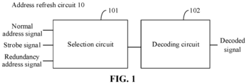
- FIG. 1 is a schematic structural diagram of an address refresh circuit according to an embodiment of the disclosure. As shown in FIG. 1 , the embodiment of the disclosure provides an address refresh circuit 10, including a selection circuit 101 and a decoding circuit 102.
- the selection circuit 101 is configured to acquire a strobe signal, a redundancy address signal and a normal address signal, and select, within each of a first pulse duration and a second pulse duration and based on the strobe signal, one of the redundancy address signal or the normal address signal as a target address signal; the first pulse duration and the second pulse duration belong to the same refresh cycle, and the second pulse duration is later than the first pulse duration.
- the decoding circuit 102 is configured to decode the target address signal to obtain and output a decoded signal.
- the redundancy address signal may correspond to Redundancy Row Address (referred to as RedRa)
- the normal address signal may correspond to Normal Row Address (referred to as Ra)
- the strobe signal may be represented as Redundancy Enable (referred to as RedEn).
- WL address refresh needs to be completed within the refresh cycle.
- the first pulse (1 st pulse) duration and the second pulse (2 nd pulse) duration belong to the same refresh cycle, and the second pulse duration is later than the first pulse duration.
- the pulse duration characterizes a refresh state, and the address refresh may be performed once correspondingly within the pulse duration.
- Ra and RedRa may share a set of circuits called the address refresh circuit 10, and both the normal address signal and the redundancy address signal are input to the selection circuit 101.
- the selection circuit 101 is configured to select the normal address signal as the target address signal within each of the first pulse duration and the second pulse duration, that is, perform refresh of Ra within the refresh cycle.
- the selection circuit 101 is configured to select the redundancy address signal as the target address signal within each of the first pulse duration and the second pulse duration, that is, perform refresh of RedRa within the refresh cycle.
- the selection circuit 101 is configured to select the redundancy address signal as the target address signal within one pulse duration and select the normal address signal as the target address signal within another pulse duration, that is, perform both refresh of Ra and refresh of RedRa within the refresh cycle.
- the refresh cycle may further include more pulse durations (e.g., a third pulse duration).
- the selection circuit 101 is configured to select one of the redundancy address signal or the normal address signal as the target address signal, within the third pulse duration and based on the strobe signal. If only two pulse durations are included within a refresh cycle, a corresponding refresh mode is referred to as two pulse refresh; and if more than two pulse durations are included within a refresh cycle, a corresponding refresh mode is referred to as multi-pulse refresh.
- the address refresh circuit 10 may select, within each of the first pulse duration and the second pulse duration and based on the strobe signal, one of the redundancy address signal or the normal address signal as the target address signal for decoding.
- the first pulse duration and the second pulse duration belong to the same refresh cycle, and address refresh may be performed once within each pulse duration, therefore, the address refresh circuit 10 may complete refresh of Ra and refresh of RedRa within the same refresh cycle, that is, the refresh of two types of row addresses is completed through a set of circuits, thereby saving consumption and improving performance.
- the selection circuit 101 includes a first selection module 201, a second selection module 202 and a third selection module 203.
- the first selection module 201 is configured to receive the redundancy address signal and the strobe signal, and output, in response to the strobe signal being at a first level, the redundancy address signal.
- the second selection module 202 is configured to receive the normal address signal and the strobe signal, and output, in response to the strobe signal being at a second level, the normal address signal.
- the third selection module 203 has input terminals connected to an output terminal of the first selection module 201 and an output terminal of the second selection module 202, respectively; and has an output terminal connected to an input terminal of the decoding circuit 102.
- a high level characterizes logical 1
- a low level characterizes logical 1
- each of the first level and the second level is the high level or the low level. Specifically, if the first level is the high level, the second level is the low level; if the first level is the low level, the second level is the high level.
- the selection circuit 101 when all the row addresses are Ra within a refresh cycle, the strobe signal is at the second level within each of the first pulse duration and the second pulse duration. Therefore, the selection circuit 101 is configured to select the normal address signal as the target address signal within each of the first pulse duration and the second pulse duration, that is, perform refresh of Ra within the refresh cycle.
- the strobe signal is at the first level within each of the first pulse duration and the second pulse duration. Therefore, the selection circuit 101 is configured to select the redundancy address signal as the target address signal within each of the first pulse duration and the second pulse duration, that is, perform refresh of RedRa within the refresh cycle.
- the strobe signal is at the first level within one pulse duration and is at the second level within another pulse duration, for example, the strobe signal is at the first level within the first pulse duration and is at the second level within the second pulse duration.
- the selection circuit 101 is configured to select the redundancy address signal as the target address signal within the first pulse duration and select the normal address signal as the target address signal within the second pulse duration, that is, perform both refresh of Ra and refresh of RedRa within the refresh cycle.
- the first selection module 201 is configured to output the redundancy address signal based on the first level of the strobe signal
- the second selection module 202 is configured to output the normal address signal based on the second level of the strobe signal. That is, the selection circuit 101 is configured to output a corresponding address signal based on a level state of the strobe signal. Therefore, one of the redundancy address signal or the normal address signal may be output within each pulse duration to complete refresh, so that refresh of the redundancy address signal and refresh of the normal address signal may be completed within the refresh cycle including the first pulse duration and the second pulse duration, respectively, thereby saving consumption and improving performance.
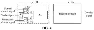
- the first selection module 201 includes a first AND gate 401 and a first inverter 402.
- the first AND gate 401 has a first input terminal connected to an output terminal of the first inverter 402, and a second input terminal for receiving the redundancy address signal; and the first inverter 402 has an input terminal for receiving the strobe signal.
- the second selection module 202 includes a second AND gate 403 configured to receive the normal address signal and the strobe signal.
- the input terminals of the third selection module 203 are connected to an output terminal of the first AND gate 401 and an output terminal of the second AND gate 403, respectively, and the output terminal of the third selection module 203 is connected to the input terminal of the decoding circuit 102.
- the first level of the strobe signal is a low level, i.e., logical 0; and the second level of the strobe signal is a high level, i.e., logical 1.
- the first inverter 402 is configured to invert logical 0 of the strobe signal into logical 1
- the first AND gate 401 is configured to perform an AND operation on logical 1 and the redundancy address signal, to obtain a first intermediate signal 'a' characterized as the redundancy address signal
- the second AND gate 403 is configured to perform an AND operation on logical 0 of the strobe signal and the normal address signal, to obtain a second intermediate signal 'b' set to logical 0, that is, to mask the normal address signal.
- the first inverter 402 is configured to invert logical 1 of the strobe signal into logical 0, and the first AND gate 401 is configured to perform an AND operation on logical 0 and the redundancy address signal, to obtain a first intermediate signal 'a' set to logical 0, that is, to mask the redundancy address signal; and the second AND gate 403 is configured to perform an AND operation on logical 1 of the strobe signal and the normal address signal, to obtain a second intermediate signal 'b' characterized as the normal address signal.
- the second AND gate 403 has an input terminal for receiving other signals to adjust an output result of the second AND gate 403.
- the output terminal of the first inverter 402 may be switched to be connected to an input terminal of the second AND gate 403.
- the normal address signal is output if the strobe signal is at logical 0
- the redundancy address signal is output if the strobe signal is at logical 1.
- each of the first AND gate 401 and the second AND gate 403 may be replaced with an OR gate. All of the above transformations shall fall within the scope of protection of the disclosure.
- the normal address signal may be masked and the redundancy address signal may be output when the strobe signal is at logical 0; and the redundancy address signal is masked and the normal address signal is output when the strobe signal is at logical 0. Therefore, it is achieved that a corresponding address signal is output based on the level state of the strobe signal, so that refresh of the redundancy address signal and refresh of the normal address signal may be completed within the refresh cycle including the first pulse duration and the second pulse duration, respectively, thereby saving consumption and improving performance.
- the third selection module 203 includes a NOT-OR (NOR) gate 404 and a second inverter 405.
- the NOR gate 404 has an output terminal connected to an input terminal of the second inverter 405, and input terminals taken as the input terminals of the third selection module 203; and the second inverter 405 has an output terminal taken as the output terminal of the third selection module 203.
- the NOR gate 404 and the second inverter 405 are configured to perform an OR operation on the first intermediate signal 'a' and the second intermediate signal 'b', to obtain and output the redundancy address signal as the target address signal.
- the NOR gate 404 and the second inverter 405 are configured to perform an OR operation on the first intermediate signal 'a' and the second intermediate signal 'b', to obtain and output the normal address signal as the target address signal.
- the second inverter 405 may be configured to drive the output target address signal, to reduce attenuation of the target address signal during transmission.
- each of the first AND gate 401 and the second AND gate 403 is replaced with an OR gate
- the NOR gate 404 is required to be replaced with a NOT-AND (NAND) gate correspondingly, and the circuit after such replacement may still select, based on the level state of the strobe signal, one of the redundancy address signal or the normal address signal as the target address signal for outputting. All of the above transformations shall fall within the scope of protection of the disclosure.
- one of the redundancy address signal or the normal address signal may be selected, based on the level state of the strobe signal, as the target address signal for outputting, so that refresh of the redundancy address signal and refresh of the normal address signal may be completed within the refresh cycle including the first pulse duration and the second pulse duration, respectively, thereby saving consumption and improving performance.
- the decoding circuit 102 includes an enable module 204 and a decoder 301.
- the enable module 204 is connected to an output terminal of the selection circuit 101, and is configured to receive an enable signal and output, in response to the enable signal being at a second level, the received target address signal.
- the decoder 301 is connected to an output terminal of the enable module 204, and is configured to decode the target address signal to obtain and output the decoded signal.
- the enable module 204 has a first input terminal connected to the output terminal of the selection circuit 101 to receive the target address signal, and a second input terminal for receiving the enable signal, and the enable module 204 is configured to output the received target address signal in response to the enable signal being at the second level. That is, the enable module 204 may control the output of the target address signal based on the level of the enable signal.
- the decoded signal output by the decoder 301 may characterize position information of a row address to be refreshed.
- a refresh module may determine and refresh a corresponding row address based on the decoded signal.
- the enable module 204 may control the output of the target address signal based on the level of the enable signal. Therefore, timing of the target address signal may be adjusted to improve timing state of the signal.
- the enable module 204 includes a NAND gate 406 and a third inverter 407.
- the NAND gate 406 has a first input terminal, which is taken as the first input terminal of the enable module 204, for receiving the enable signal, a second input terminal taken as the second input terminal of the enable module 204 and connected to the output terminal of the selection circuit 101, and an output terminal connected to an input terminal of the third inverter 407.
- the third inverter 407 has an output terminal taken as the output terminal of the enable module 204 and connected to the decoder 301.
- the input terminals of the NAND gate 406 are configured to receive the enable signal and the target address signal, and the second level of the enable signal is a high level, i.e., logical 1.
- the NAND gate 406 and the third inverter 407 are configured to perform an AND operation on the enable signal and the target address signal. If the enable signal is at the second level, i.e., logical 1, the third inverter 407 is configured to output the target address signal subjected to the AND operation; and if the enable signal is at logical 0, the third inverter 407 is configured to output logical 0, that is, the target address signal is masked.
- the third inverter 407 may drive the output target address signal, to reduce attenuation of the target address signal during transmission.
- the NAND gate 406 may be replaced with a NOR gate. After such replacement, the received target address signal is output when the enable signal is at logical 0. Therefore, the output of the target address signal may be controlled based on the level of the enable signal. Correspondingly, subsequent modules may identify the target address signal. If the target address signal is always at logical 1, the target address signal is determined as an invalid signal, and the address refresh operation is not performed. All of the above transformations shall fall within the scope of protection of the disclosure.
- the NAND gate 406 and the third inverter 407 may perform an AND operation on the enable signal and the target address signal, output the target address signal when the enable signal is at logical 1, and masks the target address signal when the enable signal is at logical 0. Therefore, it is achieved that the output of the target address signal is controlled based on the level of the enable signal, so that timing of the target address signal may be adjusted to improve timing state of the signal.
- the second inverter 405 has the output terminal taken as the output terminal of the selection circuit 101 and connected to the second input terminal of the NAND gate 406.
- the first AND gate 401 has the input terminals for receiving an inverted signal of the strobe signal and the redundancy address signal
- the second AND gate 403 is configured to receive the normal address signal and the strobe signal
- the output terminal of the first AND gate 401 and the output terminal of the second AND gate 403 are connected to two input terminals of the NOR gate 404, respectively.
- the second inverter 405 is configured to output, to the first input terminal of the NAND gate 406, the redundancy address signal as the target address signal
- the second inverter 405 is configured to output, to the first input terminal of the NAND gate 406, the normal address signal as the target address signal. Therefore, during each pulse duration within a refresh cycle, refresh of RedRa or refresh of Ra may be achieved by controlling the level of the strobe signal.
- the first input terminal of the NAND gate 406 is configured to receive the target address signal
- the second input terminal of the NAND gate 406 is configured to receive the enable signal.
- the third inverter 407 is configured to output the target address signal to the decoder 301 for decoding. Therefore, timing of the target address signal may be adjusted based on the enable signal, to improve timing state of the signal.
- FIG. 9 is an optional schematic flowchart of an address refresh method according to an embodiment of the disclosure, which will be described with reference to operations shown in FIG. 9 .
- a strobe signal, a redundancy address signal and a normal address signal are acquired, respectively.
- the selection circuit 101 may be configured to acquire the strobe signal, the redundancy address signal and the normal address signal, respectively.
- the redundancy address signal may correspond to a redundancy row address (referred to as RedRa)
- the normal address signal may correspond to a normal row address (referred to as Ra).
- one of the redundancy address signal or the normal address signal is selected as a target address signal, within each of a first pulse duration and a second pulse duration and based on the strobe signal; the first pulse duration and the second pulse duration belong to the same refresh cycle, and the second pulse duration is later than the first pulse duration.
- the pulse duration characterizes a refresh state and address refresh may be performed once correspondingly within the pulse duration. That is, the selection circuit 101 may be configured to refresh one of RedRa or Ra within each of the first pulse duration and the second pulse duration. Therefore, refresh of the redundancy address signal and refresh of the normal address signal may be completed within a refresh cycle, respectively.
- the target address signal is decoded to obtain and output a decoded signal.
- the decoding circuit 102 may be configured to decode the target address signal, to obtain and output the decoded signal.
- the decoded signal characterizes position information of a row address to be refreshed. A corresponding row address may be determined and refreshed based on the decoded signal.
- one of the redundancy address signal or the normal address signal may be selected as the target address signal for decoding.
- the first pulse duration and the second pulse duration belong to the same refresh cycle, and address refresh may be performed once within each pulse duration, therefore, according to the embodiment of the disclosure, refresh of Ra and refresh of RedRa may be completed within the same refresh cycle, that is, refresh of two types of row addresses may be completed through a set of circuits, thereby saving consumption and improving performance.
- the operation S103 shown in FIG. 9 may be implemented by an operation S1031, which will be described with reference to the following operation.
- the enable module 204 may be configured to control the output of the target address signal based on the level of the enable signal.
- the second input terminal of the enable module 204 is configured to receive the enable signal, and if the enable signal is at the second level, the enable module 204 is configured to output the received target address signal to the decoder 301; and the decoder 301 is configured to decode the target address signal and outputs the decoded signal.
- the output of the target address signal is controlled based on the level of the enable signal. Therefore, timing of the target address signal may be adjusted to improve timing state of the signal.
- the refresh cycle may further include a third pulse duration; and an operation S 104 is further included after the operation S101 shown in FIG. 9 , which will be described with reference to the following operation.
- one of the redundancy address signal or the normal address signal is selected as the target address signal, within the third pulse duration and based on the strobe signal.
- the refresh cycle may further include more pulse durations (e.g., the third pulse duration).
- the selection circuit 101 may be configured to select one of the redundancy address signal or the normal address signal as the target address signal, within the third pulse duration and based on the strobe signal.
- the operation S102 shown in FIG. 9 may be implemented by operations S1021 ⁇ S1022 shown in FIG. 10 , which will be described with reference to the following operations.
- the redundancy address signal is output as the target address signal, if the strobe signal is at a first level.
- the selection circuit 101 may be configured to output the redundancy address signal as the target address signal, when the strobe signal is at the first level.
- the normal address signal is output as the target address signal, if the strobe signal is at a second level.
- the selection circuit 101 may be configured to output the normal address signal as the target address signal, when the strobe signal is at the second level.
- each of the first level and the second level is a high level or a low level.
- the selection circuit 101 may be configured to implement, through an AND gate or an OR gate, the process of selecting the target address signal based on the level state of the strobe signal, which is not limited here.
- a corresponding address signal is output based on the level state of the strobe signal. Therefore, one of the redundancy address signal or the normal address signal may be output within each pulse duration to complete refresh, so that refresh of the redundancy address signal and refresh of the normal address signal may be completed within the refresh cycle including the first pulse duration and the second pulse duration, respectively, thereby saving consumption and improving performance.
- the first level characterizes logical 0; and the operation S 1021 shown in FIG. 10 may be implemented by operations S201 ⁇ S203 shown in FIG. 11 , which will be described with reference to the following operations.
- the first level of the strobe signal is inverted, and an AND operation is performed on the inverted first level of the strobe signal and the redundancy address signal, to obtain a first intermediate signal characterized as the redundancy address signal.
- the selection circuit 101 may be configured to invert logical 0 of the strobe signal into logical 1 through the first inverter 402; and configured to perform the AND operation on logical 1 and the redundancy address signal through the first AND gate 401, to obtain the first intermediate signal 'a' characterized as the redundancy address signal.
- an AND operation is performed on the first level of the strobe signal and the normal address signal, to obtain a second intermediate signal set to be at the first level.
- the selection circuit 101 may be configured to perform the AND operation on logical 0 of the strobe signal and the normal address signal through the second AND gate 403, to obtain the second intermediate signal 'b' set to logical 0, that is, to mask the normal address signal.
- an OR operation is performed on the first intermediate signal characterized as the redundancy address signal and the second intermediate signal set to be at the first level, to obtain the target address signal characterized as the redundancy address signal.
- the selection circuit 101 may be configured to perform the OR operation on the first intermediate signal 'a' and the second intermediate signal 'b' through the NOR gate 404 and the second inverter 405, to obtain and output the redundancy address signal as the target address signal.
- the second level characterizes logical 1; and the operation S1022 shown in FIG. 10 may be implemented by operations S301 ⁇ S303 shown in FIG. 12 , which will be described with reference to the following operations.
- the second level of the strobe signal is inverted, and an AND operation is performed on the inverted second level of the strobe signal and the redundancy address signal, to obtain a first intermediate signal set to be at the first level.
- the selection circuit 101 may be configured to invert logical 1 of the strobe signal into logical 0 through the first inverter 402; and configured to perform the AND operation on logical 0 and the redundancy address signal through the first AND gate 401, to obtain the first intermediate signal 'a' set to logical 0, that is, to mask the redundancy address signal.
- an AND operation is performed on the second level of the strobe signal and the normal address signal, to obtain a second intermediate signal characterized as the normal address signal.
- the selection circuit 101 may be configured to perform the AND operation on logical 1 of the strobe signal and the normal address signal through the second AND gate 403, to obtain the second intermediate signal 'b' characterized as the normal address signal.
- an OR operation is performed on the first intermediate signal set to be at the first level and the second intermediate signal characterized as the normal address signal, to obtain the target address signal characterized as the normal address signal.
- the selection circuit 101 may be configured to perform the OR operation on the first intermediate signal 'a' and the second intermediate signal 'b' through the NOR gate 404 and the second inverter 405, to obtain and output the normal address signal as the target address signal.
- one of the redundancy address signal or the normal address signal may be selected, based on level state of the strobe signal, as the target address signal for outputting, so that refresh of the redundancy address signal and refresh of the normal address signal may be completed within the refresh period including the first pulse duration and the second pulse duration, respectively, thereby saving consumption and improving performance.
- the second level characterizes logical 1; and the operation S1031 in the above-described embodiment may be implemented by operations S401 ⁇ S402 shown in FIG. 13 , which will be described with reference to the following operations.
- the enable module 204 may be configured to perform the AND operation on the enable signal and the target address signal through the NAND gate 406 and the third inverter 407. If the enable signal is at the second level, i.e., logical 1, the third inverter 407 is configured to output the target address signal subjected to the AND operation; and if the enable signal is at logical 0, the third inverter 407 is configured to output logical 0, that is, the target address signal is masked.
- the target address signal is decoded by the decoder, to obtain and output the decoded signal.
- the decoder 301 may be configured to decode the target address signal, to obtain and output the decode signal.
- the AND operation is performed on the enable signal and the target address signal through the NAND gate 406 and the third inverter 407.
- the target address signal is output when the enable signal is at logical 1
- the target address signal is masked when the enable signal is at logical 0. Therefore, it is achieved that the output of the target address signal is controlled based on the level of the enable signal, so that timing of the target address signal may be adjusted to improve timing state of the signal.
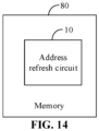
- An embodiment of the disclosure further provides a memory 80.
- the memory 80 includes the address refresh circuit 10 in the foregoing embodiments, so that consumption may be saved and performance may be improved.
- the memory 80 shown in FIG. 14 includes at least a DRAM.
- An embodiment of the disclosure further provides an electronic device 90.
- the electronic device 90 includes the memory 80.
- the address refresh circuit provided by the embodiments of the disclosure may complete refresh of the normal row address and refresh of redundancy row address within a refresh cycle, that is, refresh of two types of row addresses may be completed through a set of circuits, thereby saving consumption and improving performance.
Landscapes
- Engineering & Computer Science (AREA)
- Microelectronics & Electronic Packaging (AREA)
- Computer Hardware Design (AREA)
- Theoretical Computer Science (AREA)
- Physics & Mathematics (AREA)
- General Engineering & Computer Science (AREA)
- General Physics & Mathematics (AREA)
- Dram (AREA)
Abstract
Description
- This application is filed based on and claims priority to
Chinese Patent Application No. 202111476366.2 filed on December 6, 2021 - The disclosure relates to the field of integrated circuits, and in particular to an address refresh circuit and method, a memory, and an electronic device.
- With the rapid development of capacities and speeds of semiconductor memory devices widely used in electronic devices, power consumption of the semiconductor memory devices has been increasing.
- The Dynamic Random Access Memory (DRAM) is a volatile semiconductor memory device that stores data by using charges stored in capacitors. Since the charges stored in the capacitors may leak in various ways over time, the DRAM has a characteristic of limited data retention. In order to solve the limited data retention, the DRAM usually needs to be refreshed periodically based on the data stored in the DRAM, to charge or discharge the capacitors.
- However, the addresses to be refreshed include a normal address and a redundancy address. How to perform the refresh of these two types of addresses will affect the performance of the DRAM.
- In view of this, embodiments of the disclosure provide an address refresh circuit and method, a memory, and an electronic device, which may perform the refresh based on at least two types of address signals within a refresh cycle, respectively, and complete unified processing of the normal address and the redundancy address, thereby saving consumption and improving performance.
- Technical solutions of the embodiments of the disclosure are implemented as follows.
- An embodiment of the disclosure provides an address refresh circuit, including a selection circuit and a decoding circuit. The selection circuit is configured to acquire a strobe signal, a redundancy address signal and a normal address signal; and select, within each of a first pulse duration and a second pulse duration and based on the strobe signal, one of the redundancy address signal or the normal address signal as a target address signal. The first pulse duration and the second pulse duration belong to the same refresh cycle, and the second pulse duration is later than the first pulse duration. The decoding circuit is configured to decode the target address signal to obtain and output a decoded signal.
- An embodiment of the disclosure further provides an address refresh method, including the following operations. A strobe signal, a redundancy address signal and a normal address signal are acquired respectively. One of the redundancy address signal or the normal address signal is selected as a target address signal, within each of a first pulse duration and a second pulse duration and based on the strobe signal. The first pulse duration and the second pulse duration belong to the same refresh cycle, and the second pulse duration is later than the first pulse duration. The target address signal is decoded to obtain and output a decoded signal.
- An embodiment of the disclosure further provides a memory, including the address refresh circuit in above-mentioned embodiment.
- An embodiment of the disclosure further provides an electronic device, including the memory in the above-mentioned embodiment.
- As can be seen, the embodiments of the disclosure provide an address refresh circuit and method, a memory, and an electronic device, including a selection circuit and a decoding circuit. The selection circuit is configured to acquire a strobe signal, a redundancy address signal and a normal address signal, and select, within each of a first pulse duration and a second pulse duration and based on the strobe signal, one of the redundancy address signal or the normal address signal as a target address signal; the first pulse duration and the second pulse duration belong to the same refresh cycle, and the second pulse duration is later than the first pulse duration. The decoding circuit is configured to decode the target address signal, to obtain and output a decoded signal. Because the first pulse duration and the second pulse duration belong to the same refresh cycle and address refresh is performed once within each pulse duration, the address refresh circuit provided in the embodiments of the disclosure may complete refresh of Normal Row Address (Ra) and refresh of Redundancy Row Address (RedRa) within the same refresh cycle, that is, refresh of two types of row addresses may be completed through a set of circuits, thereby saving consumption and improving performance.
-
-
FIG. 1 is a first schematic structural diagram of an address refresh circuit according to an embodiment of the disclosure. -
FIG. 2 is a schematic analysis diagram of an address refresh circuit according to an embodiment of the disclosure. -
FIG. 3 is a second schematic structural diagram of an address refresh circuit according to an embodiment of the disclosure. -
FIG. 4 is a third schematic structural diagram of an address refresh circuit according to an embodiment of the disclosure. -
FIG. 5 is a fourth schematic structural diagram of an address refresh circuit according to an embodiment of the disclosure. -
FIG. 6 is a fifth schematic structural diagram of an address refresh circuit according to an embodiment of the disclosure. -
FIG. 7 is a sixth schematic structural diagram of an address refresh circuit according to an embodiment of the disclosure. -
FIG. 8 is a seventh schematic structural diagram of an address refresh circuit according to an embodiment of the disclosure. -
FIG. 9 is a first flowchart of an address refresh method according to an embodiment of the disclosure. -
FIG. 10 is a second flowchart of an address refresh method according to an embodiment of the disclosure. -
FIG. 11 is a third flowchart of an address refresh method according to an embodiment of the disclosure. -
FIG. 12 is a fourth flowchart of an address refresh method according to an embodiment of the disclosure. -
FIG. 13 is a fifth flowchart of an address refresh method according to an embodiment of the disclosure. -
FIG. 14 is a schematic structural diagram of a memory according to an embodiment of the disclosure. -
FIG. 15 is a schematic structural diagram of an electronic device according to an embodiment of the disclosure. - In order to make the objective, technical solutions and advantages of the disclosure clearer, the technical solutions of the disclosure are further described in detail below with reference to the accompanying drawings and embodiments. The described embodiments shall not be construed as limitation of the disclosure. All other embodiments obtained by those of ordinary skill in the art without paying any creative work shall fall within the scope of protection of the disclosure.
- In the following descriptions, reference is made to "some embodiments" which describe a subset of all possible embodiments. However, it should be understood that "some embodiments" may be the same or different subsets of all possible embodiments and may be combined with each other without conflict.
- If "first/second" or a similar description appears in the disclosure, the following explanations are added. In the following descriptions, the term "first/second/third" involved is intended only to distinguish similar objects and does not represent a specific order for the objects. It should be understood that "first/second/third" may be interchanged in a specific order or sequence where allowed, so that the embodiments of the disclosure described here may be implemented in an order other than those illustrated or described here.
- Unless otherwise defined, all technical and scientific terms used here have the same meaning as usually understood by one of ordinary skilled in the technical field to which the disclosure belongs to. The terms used here are intended to describe the embodiments of the disclosure only, and are not intended to limit the disclosure.
- When a DRAM performs a refresh operation, the DRAM may refresh several word lines (WLs) simultaneously at a time. For example, if R15, R15B, R14 and R14B in a decoding circuit are all set to be 1 simultaneously, four WLs may be refreshed simultaneously at a time. There may be normal addresses and redundancy addresses in these WLs, that is, some of the addresses in the WLs are replaced with the redundancy addresses.
- In the related art, the normal address and the redundancy address are usually refreshed separately, which requires additional refresh commands (CMDs), thereby occupying bandwidth resources and losing cell retention time; or, the normal address and the redundancy address are refreshed together, so that the normal address and the redundancy address are required to be decoded separately, which increases the area of the chip and is not beneficial to improve the integration of the chip.
-
FIG. 1 is a schematic structural diagram of an address refresh circuit according to an embodiment of the disclosure. As shown inFIG. 1 , the embodiment of the disclosure provides anaddress refresh circuit 10, including aselection circuit 101 and adecoding circuit 102. - The
selection circuit 101 is configured to acquire a strobe signal, a redundancy address signal and a normal address signal, and select, within each of a first pulse duration and a second pulse duration and based on the strobe signal, one of the redundancy address signal or the normal address signal as a target address signal; the first pulse duration and the second pulse duration belong to the same refresh cycle, and the second pulse duration is later than the first pulse duration. - The
decoding circuit 102 is configured to decode the target address signal to obtain and output a decoded signal. - In the embodiment of the disclosure, the redundancy address signal may correspond to Redundancy Row Address (referred to as RedRa), the normal address signal may correspond to Normal Row Address (referred to as Ra), and the strobe signal may be represented as Redundancy Enable (referred to as RedEn).
- In the embodiment of the disclosure, as shown in
FIG. 2 , there is a refresh cycle between a refresh command (REFCmd) and an active command (Active), and WL address refresh needs to be completed within the refresh cycle. The first pulse (1st pulse) duration and the second pulse (2nd pulse) duration belong to the same refresh cycle, and the second pulse duration is later than the first pulse duration. The pulse duration characterizes a refresh state, and the address refresh may be performed once correspondingly within the pulse duration. - In the embodiment of the disclosure, Ra and RedRa may share a set of circuits called the
address refresh circuit 10, and both the normal address signal and the redundancy address signal are input to theselection circuit 101. When all the row addresses are Ra within a refresh cycle, theselection circuit 101 is configured to select the normal address signal as the target address signal within each of the first pulse duration and the second pulse duration, that is, perform refresh of Ra within the refresh cycle. When all the row addresses are RedRa within a refresh cycle, theselection circuit 101 is configured to select the redundancy address signal as the target address signal within each of the first pulse duration and the second pulse duration, that is, perform refresh of RedRa within the refresh cycle. When both RedRa and Ra are present within a refresh cycle, theselection circuit 101 is configured to select the redundancy address signal as the target address signal within one pulse duration and select the normal address signal as the target address signal within another pulse duration, that is, perform both refresh of Ra and refresh of RedRa within the refresh cycle. - It should be noted that in an embodiment of the disclosure, the refresh cycle may further include more pulse durations (e.g., a third pulse duration). Correspondingly, the
selection circuit 101 is configured to select one of the redundancy address signal or the normal address signal as the target address signal, within the third pulse duration and based on the strobe signal. If only two pulse durations are included within a refresh cycle, a corresponding refresh mode is referred to as two pulse refresh; and if more than two pulse durations are included within a refresh cycle, a corresponding refresh mode is referred to as multi-pulse refresh. - It should be understood that the
address refresh circuit 10 may select, within each of the first pulse duration and the second pulse duration and based on the strobe signal, one of the redundancy address signal or the normal address signal as the target address signal for decoding. The first pulse duration and the second pulse duration belong to the same refresh cycle, and address refresh may be performed once within each pulse duration, therefore, theaddress refresh circuit 10 may complete refresh of Ra and refresh of RedRa within the same refresh cycle, that is, the refresh of two types of row addresses is completed through a set of circuits, thereby saving consumption and improving performance. - In some embodiments of the disclosure, as shown in
FIG. 3 , theselection circuit 101 includes afirst selection module 201, asecond selection module 202 and athird selection module 203. Thefirst selection module 201 is configured to receive the redundancy address signal and the strobe signal, and output, in response to the strobe signal being at a first level, the redundancy address signal. Thesecond selection module 202 is configured to receive the normal address signal and the strobe signal, and output, in response to the strobe signal being at a second level, the normal address signal. Thethird selection module 203 has input terminals connected to an output terminal of thefirst selection module 201 and an output terminal of thesecond selection module 202, respectively; and has an output terminal connected to an input terminal of thedecoding circuit 102. - In the embodiment of the disclosure, a high level characterizes logical 1, a low level characterizes logical 0, and each of the first level and the second level is the high level or the low level. Specifically, if the first level is the high level, the second level is the low level; if the first level is the low level, the second level is the high level.
- In the embodiment of the disclosure, when all the row addresses are Ra within a refresh cycle, the strobe signal is at the second level within each of the first pulse duration and the second pulse duration. Therefore, the
selection circuit 101 is configured to select the normal address signal as the target address signal within each of the first pulse duration and the second pulse duration, that is, perform refresh of Ra within the refresh cycle. When all the row addresses are RedRa within a refresh cycle, the strobe signal is at the first level within each of the first pulse duration and the second pulse duration. Therefore, theselection circuit 101 is configured to select the redundancy address signal as the target address signal within each of the first pulse duration and the second pulse duration, that is, perform refresh of RedRa within the refresh cycle. When both RedRa and Ra are present within a refresh cycle, the strobe signal is at the first level within one pulse duration and is at the second level within another pulse duration, for example, the strobe signal is at the first level within the first pulse duration and is at the second level within the second pulse duration. At this time, theselection circuit 101 is configured to select the redundancy address signal as the target address signal within the first pulse duration and select the normal address signal as the target address signal within the second pulse duration, that is, perform both refresh of Ra and refresh of RedRa within the refresh cycle. - It should be understood that the
first selection module 201 is configured to output the redundancy address signal based on the first level of the strobe signal, and thesecond selection module 202 is configured to output the normal address signal based on the second level of the strobe signal. That is, theselection circuit 101 is configured to output a corresponding address signal based on a level state of the strobe signal. Therefore, one of the redundancy address signal or the normal address signal may be output within each pulse duration to complete refresh, so that refresh of the redundancy address signal and refresh of the normal address signal may be completed within the refresh cycle including the first pulse duration and the second pulse duration, respectively, thereby saving consumption and improving performance. - In some embodiments of the disclosure, as shown in
FIG. 4 , thefirst selection module 201 includes a first ANDgate 401 and afirst inverter 402. The first ANDgate 401 has a first input terminal connected to an output terminal of thefirst inverter 402, and a second input terminal for receiving the redundancy address signal; and thefirst inverter 402 has an input terminal for receiving the strobe signal. Thesecond selection module 202 includes a second ANDgate 403 configured to receive the normal address signal and the strobe signal. The input terminals of thethird selection module 203 are connected to an output terminal of the first ANDgate 401 and an output terminal of the second ANDgate 403, respectively, and the output terminal of thethird selection module 203 is connected to the input terminal of thedecoding circuit 102. - In the embodiment of the disclosure, the first level of the strobe signal is a low level, i.e., logical 0; and the second level of the strobe signal is a high level, i.e., logical 1. If the strobe signal is at logical 0, the
first inverter 402 is configured to invert logical 0 of the strobe signal into logical 1, and the first ANDgate 401 is configured to perform an AND operation on logical 1 and the redundancy address signal, to obtain a first intermediate signal 'a' characterized as the redundancy address signal; and the second ANDgate 403 is configured to perform an AND operation on logical 0 of the strobe signal and the normal address signal, to obtain a second intermediate signal 'b' set to logical 0, that is, to mask the normal address signal. If the strobe signal is at logical 1, thefirst inverter 402 is configured to invert logical 1 of the strobe signal into logical 0, and the first ANDgate 401 is configured to perform an AND operation on logical 0 and the redundancy address signal, to obtain a first intermediate signal 'a' set to logical 0, that is, to mask the redundancy address signal; and the second ANDgate 403 is configured to perform an AND operation on logical 1 of the strobe signal and the normal address signal, to obtain a second intermediate signal 'b' characterized as the normal address signal. - In an embodiment of the disclosure, the second AND
gate 403 has an input terminal for receiving other signals to adjust an output result of the second ANDgate 403. - It should be noted that the output terminal of the
first inverter 402 may be switched to be connected to an input terminal of the second ANDgate 403. At this time, the normal address signal is output if the strobe signal is at logical 0, and the redundancy address signal is output if the strobe signal is at logical 1. On the other hand, each of the first ANDgate 401 and the second ANDgate 403 may be replaced with an OR gate. All of the above transformations shall fall within the scope of protection of the disclosure. - It should be understood that with the first AND
gate 401, thefirst inverter 402 and the second ANDgate 403, the normal address signal may be masked and the redundancy address signal may be output when the strobe signal is at logical 0; and the redundancy address signal is masked and the normal address signal is output when the strobe signal is at logical 0. Therefore, it is achieved that a corresponding address signal is output based on the level state of the strobe signal, so that refresh of the redundancy address signal and refresh of the normal address signal may be completed within the refresh cycle including the first pulse duration and the second pulse duration, respectively, thereby saving consumption and improving performance. - In some embodiments of the disclosure, as shown in
FIG. 5 , thethird selection module 203 includes a NOT-OR (NOR)gate 404 and asecond inverter 405. The NORgate 404 has an output terminal connected to an input terminal of thesecond inverter 405, and input terminals taken as the input terminals of thethird selection module 203; and thesecond inverter 405 has an output terminal taken as the output terminal of thethird selection module 203. - In the embodiment of the disclosure, if the strobe signal is at logical 0, the first intermediate signal 'a' is characterized as the redundancy address signal, and the second intermediate signal 'b' is set to logical 0, that is, the normal address signal is masked. At this time, the NOR
gate 404 and thesecond inverter 405 are configured to perform an OR operation on the first intermediate signal 'a' and the second intermediate signal 'b', to obtain and output the redundancy address signal as the target address signal. - If the strobe signal is at logical 1, the first intermediate signal 'a' is set to logical 0, that is, the redundancy address signal is masked, and the second intermediate signal 'b' is characterized as the normal address signal. At this time, the NOR
gate 404 and thesecond inverter 405 are configured to perform an OR operation on the first intermediate signal 'a' and the second intermediate signal 'b', to obtain and output the normal address signal as the target address signal. - In the embodiment of the disclosure, the
second inverter 405 may be configured to drive the output target address signal, to reduce attenuation of the target address signal during transmission. - It should be noted that if each of the first AND
gate 401 and the second ANDgate 403 is replaced with an OR gate, the NORgate 404 is required to be replaced with a NOT-AND (NAND) gate correspondingly, and the circuit after such replacement may still select, based on the level state of the strobe signal, one of the redundancy address signal or the normal address signal as the target address signal for outputting. All of the above transformations shall fall within the scope of protection of the disclosure. - It should be understood that with the first AND
gate 401, thefirst inverter 402, the second ANDgate 403, the NORgate 404 and thesecond inverter 405, one of the redundancy address signal or the normal address signal may be selected, based on the level state of the strobe signal, as the target address signal for outputting, so that refresh of the redundancy address signal and refresh of the normal address signal may be completed within the refresh cycle including the first pulse duration and the second pulse duration, respectively, thereby saving consumption and improving performance. - In some embodiments of the disclosure, as shown in
FIG. 6 , thedecoding circuit 102 includes an enablemodule 204 and adecoder 301. The enablemodule 204 is connected to an output terminal of theselection circuit 101, and is configured to receive an enable signal and output, in response to the enable signal being at a second level, the received target address signal. Thedecoder 301 is connected to an output terminal of the enablemodule 204, and is configured to decode the target address signal to obtain and output the decoded signal. - In the embodiment of the disclosure, the enable
module 204 has a first input terminal connected to the output terminal of theselection circuit 101 to receive the target address signal, and a second input terminal for receiving the enable signal, and the enablemodule 204 is configured to output the received target address signal in response to the enable signal being at the second level. That is, the enablemodule 204 may control the output of the target address signal based on the level of the enable signal. - In the embodiment of the disclosure, the decoded signal output by the
decoder 301 may characterize position information of a row address to be refreshed. A refresh module may determine and refresh a corresponding row address based on the decoded signal. - It should be understood that the enable
module 204 may control the output of the target address signal based on the level of the enable signal. Therefore, timing of the target address signal may be adjusted to improve timing state of the signal. - In some embodiments of the disclosure, as shown in
FIG. 7 , the enablemodule 204 includes aNAND gate 406 and athird inverter 407. TheNAND gate 406 has a first input terminal, which is taken as the first input terminal of the enablemodule 204, for receiving the enable signal, a second input terminal taken as the second input terminal of the enablemodule 204 and connected to the output terminal of theselection circuit 101, and an output terminal connected to an input terminal of thethird inverter 407. Thethird inverter 407 has an output terminal taken as the output terminal of the enablemodule 204 and connected to thedecoder 301. - In the embodiment of the disclosure, the input terminals of the
NAND gate 406 are configured to receive the enable signal and the target address signal, and the second level of the enable signal is a high level, i.e., logical 1. TheNAND gate 406 and thethird inverter 407 are configured to perform an AND operation on the enable signal and the target address signal. If the enable signal is at the second level, i.e., logical 1, thethird inverter 407 is configured to output the target address signal subjected to the AND operation; and if the enable signal is at logical 0, thethird inverter 407 is configured to output logical 0, that is, the target address signal is masked. - In the embodiment of the disclosure, the
third inverter 407 may drive the output target address signal, to reduce attenuation of the target address signal during transmission. - It should be noted that the
NAND gate 406 may be replaced with a NOR gate. After such replacement, the received target address signal is output when the enable signal is at logical 0. Therefore, the output of the target address signal may be controlled based on the level of the enable signal. Correspondingly, subsequent modules may identify the target address signal. If the target address signal is always at logical 1, the target address signal is determined as an invalid signal, and the address refresh operation is not performed. All of the above transformations shall fall within the scope of protection of the disclosure. - It should be understood that the
NAND gate 406 and thethird inverter 407 may perform an AND operation on the enable signal and the target address signal, output the target address signal when the enable signal is at logical 1, and masks the target address signal when the enable signal is at logical 0. Therefore, it is achieved that the output of the target address signal is controlled based on the level of the enable signal, so that timing of the target address signal may be adjusted to improve timing state of the signal. - In some embodiments of the disclosure, as shown in
FIG. 8 , thesecond inverter 405 has the output terminal taken as the output terminal of theselection circuit 101 and connected to the second input terminal of theNAND gate 406. - In the embodiment of the disclosure, the first AND
gate 401 has the input terminals for receiving an inverted signal of the strobe signal and the redundancy address signal, the second ANDgate 403 is configured to receive the normal address signal and the strobe signal, and the output terminal of the first ANDgate 401 and the output terminal of the second ANDgate 403 are connected to two input terminals of the NORgate 404, respectively. When the strobe signal is at logical 0, thesecond inverter 405 is configured to output, to the first input terminal of theNAND gate 406, the redundancy address signal as the target address signal; and when the strobe signal is at logical 1, thesecond inverter 405 is configured to output, to the first input terminal of theNAND gate 406, the normal address signal as the target address signal. Therefore, during each pulse duration within a refresh cycle, refresh of RedRa or refresh of Ra may be achieved by controlling the level of the strobe signal. - The first input terminal of the
NAND gate 406 is configured to receive the target address signal, and the second input terminal of theNAND gate 406 is configured to receive the enable signal. When the enable signal is at logical 1, thethird inverter 407 is configured to output the target address signal to thedecoder 301 for decoding. Therefore, timing of the target address signal may be adjusted based on the enable signal, to improve timing state of the signal. -
FIG. 9 is an optional schematic flowchart of an address refresh method according to an embodiment of the disclosure, which will be described with reference to operations shown inFIG. 9 . - In operation S101, a strobe signal, a redundancy address signal and a normal address signal are acquired, respectively.
- In the embodiment of the disclosure, the
selection circuit 101 may be configured to acquire the strobe signal, the redundancy address signal and the normal address signal, respectively. The redundancy address signal may correspond to a redundancy row address (referred to as RedRa), and the normal address signal may correspond to a normal row address (referred to as Ra). - In operation S102, one of the redundancy address signal or the normal address signal is selected as a target address signal, within each of a first pulse duration and a second pulse duration and based on the strobe signal; the first pulse duration and the second pulse duration belong to the same refresh cycle, and the second pulse duration is later than the first pulse duration.
- In the embodiment of the disclosure, the pulse duration characterizes a refresh state and address refresh may be performed once correspondingly within the pulse duration. That is, the
selection circuit 101 may be configured to refresh one of RedRa or Ra within each of the first pulse duration and the second pulse duration. Therefore, refresh of the redundancy address signal and refresh of the normal address signal may be completed within a refresh cycle, respectively. - In operation S103, the target address signal is decoded to obtain and output a decoded signal.
- In the embodiment of the disclosure, the
decoding circuit 102 may be configured to decode the target address signal, to obtain and output the decoded signal. The decoded signal characterizes position information of a row address to be refreshed. A corresponding row address may be determined and refreshed based on the decoded signal. - It should be understood that according to the embodiment of the disclosure, within each of the first pulse duration and the second pulse duration and based on the strobe signal, one of the redundancy address signal or the normal address signal may be selected as the target address signal for decoding. The first pulse duration and the second pulse duration belong to the same refresh cycle, and address refresh may be performed once within each pulse duration, therefore, according to the embodiment of the disclosure, refresh of Ra and refresh of RedRa may be completed within the same refresh cycle, that is, refresh of two types of row addresses may be completed through a set of circuits, thereby saving consumption and improving performance.
- In some embodiments of the disclosure, the operation S103 shown in
FIG. 9 may be implemented by an operation S1031, which will be described with reference to the following operation. - In operation S1031, if an acquired enable signal is at a second level, the target address signal is decoded to obtain and output the decoded signal.
- In the embodiment of the disclosure, the enable
module 204 may be configured to control the output of the target address signal based on the level of the enable signal. Referring toFIG. 6 , the second input terminal of the enablemodule 204 is configured to receive the enable signal, and if the enable signal is at the second level, the enablemodule 204 is configured to output the received target address signal to thedecoder 301; and thedecoder 301 is configured to decode the target address signal and outputs the decoded signal. - It should be understood that the output of the target address signal is controlled based on the level of the enable signal. Therefore, timing of the target address signal may be adjusted to improve timing state of the signal.
- In some embodiments of the disclosure, the refresh cycle may further include a third pulse duration; and an operation S 104 is further included after the operation S101 shown in
FIG. 9 , which will be described with reference to the following operation. - In operation S104, one of the redundancy address signal or the normal address signal is selected as the target address signal, within the third pulse duration and based on the strobe signal.
- In the embodiment of the disclosure, the refresh cycle may further include more pulse durations (e.g., the third pulse duration). Correspondingly, the
selection circuit 101 may be configured to select one of the redundancy address signal or the normal address signal as the target address signal, within the third pulse duration and based on the strobe signal. - It should be understood that according to the embodiment of the disclosure, more than two pulse durations may be included within a refresh cycle, and a corresponding refresh mode is referred to as multi-pulse refresh.
- In some embodiments of the disclosure, the operation S102 shown in
FIG. 9 may be implemented by operations S1021 ~ S1022 shown inFIG. 10 , which will be described with reference to the following operations. - In operation S1021, the redundancy address signal is output as the target address signal, if the strobe signal is at a first level.
- In the embodiment of the disclosure, the
selection circuit 101 may be configured to output the redundancy address signal as the target address signal, when the strobe signal is at the first level. - In operation S1022, the normal address signal is output as the target address signal, if the strobe signal is at a second level.
- In the embodiment of the disclosure, the
selection circuit 101 may be configured to output the normal address signal as the target address signal, when the strobe signal is at the second level. - It should be noted that each of the first level and the second level is a high level or a low level. The
selection circuit 101 may be configured to implement, through an AND gate or an OR gate, the process of selecting the target address signal based on the level state of the strobe signal, which is not limited here. - It should be understood that a corresponding address signal is output based on the level state of the strobe signal. Therefore, one of the redundancy address signal or the normal address signal may be output within each pulse duration to complete refresh, so that refresh of the redundancy address signal and refresh of the normal address signal may be completed within the refresh cycle including the first pulse duration and the second pulse duration, respectively, thereby saving consumption and improving performance.
- In some embodiments of the disclosure, the first level characterizes logical 0; and the operation S 1021 shown in
FIG. 10 may be implemented by operations S201 ~ S203 shown inFIG. 11 , which will be described with reference to the following operations. - In operation S201, the first level of the strobe signal is inverted, and an AND operation is performed on the inverted first level of the strobe signal and the redundancy address signal, to obtain a first intermediate signal characterized as the redundancy address signal.
- In the embodiment of the disclosure, referring to
FIG. 5 , theselection circuit 101 may be configured to invert logical 0 of the strobe signal into logical 1 through thefirst inverter 402; and configured to perform the AND operation on logical 1 and the redundancy address signal through the first ANDgate 401, to obtain the first intermediate signal 'a' characterized as the redundancy address signal. - In operation S202, an AND operation is performed on the first level of the strobe signal and the normal address signal, to obtain a second intermediate signal set to be at the first level.
- In the embodiment of the disclosure, referring to
FIG. 5 , theselection circuit 101 may be configured to perform the AND operation on logical 0 of the strobe signal and the normal address signal through the second ANDgate 403, to obtain the second intermediate signal 'b' set to logical 0, that is, to mask the normal address signal. - In operation S203, an OR operation is performed on the first intermediate signal characterized as the redundancy address signal and the second intermediate signal set to be at the first level, to obtain the target address signal characterized as the redundancy address signal.
- In the embodiment of the disclosure, referring to
FIG. 5 , theselection circuit 101 may be configured to perform the OR operation on the first intermediate signal 'a' and the second intermediate signal 'b' through the NORgate 404 and thesecond inverter 405, to obtain and output the redundancy address signal as the target address signal. - In some embodiments of the disclosure, the second level characterizes logical 1; and the operation S1022 shown in
FIG. 10 may be implemented by operations S301 ~ S303 shown inFIG. 12 , which will be described with reference to the following operations. - In operation S301, the second level of the strobe signal is inverted, and an AND operation is performed on the inverted second level of the strobe signal and the redundancy address signal, to obtain a first intermediate signal set to be at the first level.
- In the embodiment of the disclosure, referring to
FIG. 5 , theselection circuit 101 may be configured to invert logical 1 of the strobe signal into logical 0 through thefirst inverter 402; and configured to perform the AND operation on logical 0 and the redundancy address signal through the first ANDgate 401, to obtain the first intermediate signal 'a' set to logical 0, that is, to mask the redundancy address signal. - In operation S302, an AND operation is performed on the second level of the strobe signal and the normal address signal, to obtain a second intermediate signal characterized as the normal address signal.
- In the embodiment of the disclosure, referring to
FIG. 5 , theselection circuit 101 may be configured to perform the AND operation on logical 1 of the strobe signal and the normal address signal through the second ANDgate 403, to obtain the second intermediate signal 'b' characterized as the normal address signal. - In operation S303, an OR operation is performed on the first intermediate signal set to be at the first level and the second intermediate signal characterized as the normal address signal, to obtain the target address signal characterized as the normal address signal.
- In the embodiment of the disclosure, referring to
FIG. 5 , theselection circuit 101 may be configured to perform the OR operation on the first intermediate signal 'a' and the second intermediate signal 'b' through the NORgate 404 and thesecond inverter 405, to obtain and output the normal address signal as the target address signal. - It should be understood that with the first AND
gate 401, thefirst inverter 402, the second ANDgate 403, the NORgate 404 and thesecond inverter 405, one of the redundancy address signal or the normal address signal may be selected, based on level state of the strobe signal, as the target address signal for outputting, so that refresh of the redundancy address signal and refresh of the normal address signal may be completed within the refresh period including the first pulse duration and the second pulse duration, respectively, thereby saving consumption and improving performance. - In some embodiments of the disclosure, the second level characterizes logical 1; and the operation S1031 in the above-described embodiment may be implemented by operations S401 ~ S402 shown in
FIG. 13 , which will be described with reference to the following operations. - In operation S401, an AND operation is performed on the target address signal and the acquired enable signal, and the target address signal is output to the decoder if the enable signal is at the second level.
- In the embodiment of the disclosure, referring to
FIG. 7 , when the enable signal is at logical 1, the enablemodule 204 may be configured to perform the AND operation on the enable signal and the target address signal through theNAND gate 406 and thethird inverter 407. If the enable signal is at the second level, i.e., logical 1, thethird inverter 407 is configured to output the target address signal subjected to the AND operation; and if the enable signal is at logical 0, thethird inverter 407 is configured to output logical 0, that is, the target address signal is masked. - In operation S402, the target address signal is decoded by the decoder, to obtain and output the decoded signal.
- In the embodiment of the disclosure, the
decoder 301 may be configured to decode the target address signal, to obtain and output the decode signal. - It should be understood that the AND operation is performed on the enable signal and the target address signal through the
NAND gate 406 and thethird inverter 407. In this way, the target address signal is output when the enable signal is at logical 1, and the target address signal is masked when the enable signal is at logical 0. Therefore, it is achieved that the output of the target address signal is controlled based on the level of the enable signal, so that timing of the target address signal may be adjusted to improve timing state of the signal. - An embodiment of the disclosure further provides a
memory 80. As shown inFIG. 14 , thememory 80 includes theaddress refresh circuit 10 in the foregoing embodiments, so that consumption may be saved and performance may be improved. - In some embodiments of the disclosure, the
memory 80 shown inFIG. 14 includes at least a DRAM. - An embodiment of the disclosure further provides an
electronic device 90. As shown inFIG. 15 , theelectronic device 90 includes thememory 80. - It should be noted that in the disclosure, the terms "include", "including" or any other variation thereof are intended to cover non-exclusive inclusion, such that a process, method, article, or device including a series of elements includes not only those elements but also other elements that are not listed explicitly, or elements inherent to such process, method, article, or device. Without any more limitation, an element defined by a sentence "include a ......" does not exclude other identical elements existing in a process, method, article, or device including the element.
- The above serial numbers for embodiments of the disclosure are for the purpose of description only and do not represent pros and cons of the embodiments. The methods disclosed in several method embodiments provided by the disclosure may be combined arbitrarily without conflict, to obtain new method embodiments. The features disclosed in several product embodiments provided by the disclosure may be combined arbitrarily without conflict, to obtain new product embodiments. The features disclosed in several method or device embodiments provided by the disclosure may be combined arbitrarily without conflict, to obtain new method or device embodiments.
- The above descriptions are merely specific embodiments of the disclosure. However, the scope of protection of the disclosure is not limited thereto. Any variation or replacement readily conceivable by any person skilled in the art within the technical scope of the disclosure shall fall within the scope of protection of the disclosure. Therefore, the scope of protection of the disclosure is subjected to the scope of protection of the claims.
- The address refresh circuit provided by the embodiments of the disclosure may complete refresh of the normal row address and refresh of redundancy row address within a refresh cycle, that is, refresh of two types of row addresses may be completed through a set of circuits, thereby saving consumption and improving performance.
Claims (17)
- An address refresh circuit, comprising:a selection circuit, configured to acquire a strobe signal, a redundancy address signal and a normal address signal; and select, within each of a first pulse duration and a second pulse duration and based on the strobe signal, one of the redundancy address signal or the normal address signal as a target address signal; wherein the first pulse duration and the second pulse duration belong to the same refresh cycle, and the second pulse duration is later than the first pulse duration; anda decoding circuit, configured to decode the target address signal to obtain and output a decoded signal.
- The address refresh circuit of claim 1, wherein the selection circuit comprises:a first selection module, configured to receive the redundancy address signal and the strobe signal, and output, in response to the strobe signal being at a first level, the redundancy address signal; anda second selection module, configured to receive the normal address signal and the strobe signal, and output, in response to the strobe signal being at a second level, the normal address signal.
- The address refresh circuit of claim 2, wherein the first selection module comprises a first AND gate and a first inverter, the first AND gate has a first input terminal connected to an output terminal of the first inverter and has a second input terminal for receiving the redundancy address signal, and the first inverter has an input terminal for receiving the strobe signal;the second selection module comprises a second AND gate configured to receive the normal address signal and the strobe signal; andthe selection circuit further comprises: a third selection module, which has input terminals connected to an output terminal of the first AND gate and an output terminal of the second AND gate, respectively, and has an output terminal connected to an input terminal of the decoding circuit.
- The address refresh circuit of claim 3, wherein the third selection module comprises:a NOT-OR (NOR) gate, which has an output terminal connected to an input terminal of a second inverter, and has input terminals taken as the input terminals of the third selection module; andthe second inverter, which has an output terminal taken as the output terminal of the third selection module.
- The address refresh circuit according to claim 1, wherein the decoding circuit comprises:an enable module, connected to an output terminal of the selection circuit, and configured to receive an enable signal and output, in response to the enable signal being at a second level, the received target address signal; anda decoder, connected to an output terminal of the enable module, and configured to decode the target address signal to obtain and output the decoded signal.
- The address refresh circuit of claim 5, wherein the enable module comprises:a NOT-AND (NAND) gate, which has a first input terminal, which is taken as a first input terminal of the enable module, for receiving the enable signal, has a second input terminal taken as a second input terminal of the enable module and connected to the output terminal of the selection circuit, and has an output terminal connected to an input terminal of a third inverter; andthe third inverter, which has an output terminal taken as the output terminal of the enable module and connected to the decoder.
- The address refresh circuit of any one of claims 1-6, wherein the refresh cycle further comprises a third pulse duration, and
the selection circuit is further configured to select, within the third pulse duration and based on the strobe signal, one of the redundancy address signal or the normal address signal as the target address signal. - An address refresh method, comprising:acquiring a strobe signal, a redundancy address signal and a normal address signal, respectively;selecting, within each of a first pulse duration and a second pulse duration and based on the strobe signal, one of the redundancy address signal or the normal address signal as a target address signal; wherein the first pulse duration and the second pulse duration belong to the same refresh cycle, and the second pulse duration is later than the first pulse duration; anddecoding the target address signal to obtain and output a decoded signal.
- The address refresh method of claim 8, wherein decoding the target address signal to obtain and output the decoded signal comprises:
decoding, in response to an acquired enable signal being at a second level, the target address signal to obtain and output the decoded signal. - The address refresh method of claim 8, wherein the refresh cycle further comprises a third pulse duration; and the method further comprises:
selecting, within the third pulse duration and based on the strobe signal, one of the redundancy address signal or the normal address signal as the target address signal. - The address refresh method of claim 8, wherein selecting, based on the strobe signal, one of the redundancy address signal or the normal address signal as the target address signal comprises:outputting, in response to the strobe signal being at a first level, the redundancy address signal as the target address signal; oroutputting, in response to the strobe signal being at a second level, the normal address signal as the target address signal.
- The address refresh method of claim 11, wherein the first level characterizes logical 0; and outputting, in response to the strobe signal being at the first level, the redundancy address signal as the target address signal comprises:inverting the first level of the strobe signal, and performing an AND operation on the inverted first level of the strobe signal and the redundancy address signal, to obtain a first intermediate signal characterized as the redundancy address signal;performing an AND operation on the first level of the strobe signal and the normal address signal, to obtain a second intermediate signal set to be at the first level; andperforming an OR operation on the first intermediate signal characterized as the redundancy address signal and the second intermediate signal set to be at the first level, to obtain the target address signal characterized as the redundancy address signal.
- The address refresh method of claim 11, wherein the second level characterizes logical 1; and outputting, in response to the strobe signal being at the second level, the normal address signal as the target address signal comprises:inverting the second level of the strobe signal, and performing an AND operation on the inverted second level of the strobe signal and the redundancy address signal, to obtain a first intermediate signal set to be at a first level;performing an AND operation on the second level of the strobe signal and the normal address signal, to obtain a second intermediate signal characterized as the normal address signal; andperforming an OR operation on the first intermediate signal set to be at the first level and the second intermediate signal characterized as the normal address signal, to obtain the target address signal characterized as the normal address signal.
- The address refresh method of claim 9, wherein the second level characterizes logical 1; and decoding, in response to the acquired enable signal being at the second level, the target address signal to obtain and output the decoded signal comprises:performing an AND operation on the target address signal and the acquired enable signal, and outputting, in response to the enable signal being at the second level, the target address signal to a decoder; anddecoding, by the decoder, the target address signal to obtain and output the decoded signal.
- A memory comprising the address refresh circuit of any one of claims 1-7.
- The memory of claim 15, wherein the memory comprises at least a dynamic random access memory (DRAM).
- An electronic device comprising the memory of claim 15 or 16.
Applications Claiming Priority (2)
| Application Number | Priority Date | Filing Date | Title |
|---|---|---|---|
| CN202111476366.2A CN116230048B (en) | 2021-12-06 | 2021-12-06 | Address refreshing circuit, method, memory and electronic equipment |
| PCT/CN2022/072027 WO2023103148A1 (en) | 2021-12-06 | 2022-01-14 | Address refresh circuit, method, memory, and electronic device |
Publications (2)
| Publication Number | Publication Date |
|---|---|
| EP4276832A1 true EP4276832A1 (en) | 2023-11-15 |
| EP4276832A4 EP4276832A4 (en) | 2024-10-02 |
Family
ID=86607953
Family Applications (1)
| Application Number | Title | Priority Date | Filing Date |
|---|---|---|---|
| EP22902593.7A Withdrawn EP4276832A4 (en) | 2021-12-06 | 2022-01-14 | ADDRESS REFRESHING, METHOD, MEMORY AND ELECTRONIC DEVICE |
Country Status (2)
| Country | Link |
|---|---|
| US (1) | US12308065B2 (en) |
| EP (1) | EP4276832A4 (en) |
Family Cites Families (11)
| Publication number | Priority date | Publication date | Assignee | Title |
|---|---|---|---|---|
| JP3736779B2 (en) | 1998-02-26 | 2006-01-18 | 株式会社日立製作所 | Dynamic RAM |
| US6590822B2 (en) * | 2001-05-07 | 2003-07-08 | Samsung Electronics Co., Ltd. | System and method for performing partial array self-refresh operation in a semiconductor memory device |
| KR20150026227A (en) | 2013-09-02 | 2015-03-11 | 에스케이하이닉스 주식회사 | Semiconductor memory device |
| KR102116920B1 (en) * | 2014-03-26 | 2020-06-01 | 에스케이하이닉스 주식회사 | Semiconductor memory device and semiconductor memory system having the same |
| KR102116980B1 (en) * | 2014-07-02 | 2020-05-29 | 삼성전자 주식회사 | Semiconductor memory device for controlling refresh operation of redundancy memory cells |
| KR102471525B1 (en) | 2016-06-01 | 2022-11-28 | 에스케이하이닉스 주식회사 | Semiconductor Memory Apparatus and Refresh Method |
| US9805782B1 (en) | 2017-02-02 | 2017-10-31 | Elite Semiconductor Memory Technology Inc. | Memory device capable of determining candidate wordline for refresh and control method thereof |
| CN207489475U (en) | 2017-10-24 | 2018-06-12 | 睿力集成电路有限公司 | Refresh counter circuit, refresh counter and memory |
| US10490250B1 (en) | 2018-08-14 | 2019-11-26 | Micron Technology, Inc. | Apparatuses for refreshing memory of a semiconductor device |
| US10790005B1 (en) * | 2019-04-26 | 2020-09-29 | Micron Technology, Inc. | Techniques for reducing row hammer refresh |
| US12308068B2 (en) * | 2022-10-12 | 2025-05-20 | Changxin Memory Technologies, Inc. | Control circuit and memory |
-
2022
- 2022-01-14 EP EP22902593.7A patent/EP4276832A4/en not_active Withdrawn
- 2022-07-01 US US17/855,841 patent/US12308065B2/en active Active
Also Published As
| Publication number | Publication date |
|---|---|
| US12308065B2 (en) | 2025-05-20 |
| EP4276832A4 (en) | 2024-10-02 |
| US20230178135A1 (en) | 2023-06-08 |
Similar Documents
| Publication | Publication Date | Title |
|---|---|---|
| US6665224B1 (en) | Partial refresh for synchronous dynamic random access memory (SDRAM) circuits | |
| US9047978B2 (en) | Apparatuses and methods for selective row refreshes | |
| KR100456989B1 (en) | Semiconductor memory device, method for controlling same, and electronic information apparatus | |
| WO2007136704A2 (en) | Nand system with a data write frequency greater than a command-and-address-load frequency | |
| CN1913038A (en) | Method of controlling refresh operation in multi-port dram and a memory system using the method | |
| US9779798B1 (en) | Systems, methods, and computer programs for providing row tamper protection in a multi-bank memory cell array | |
| US11854653B2 (en) | Signal masking circuit and semiconductor memory | |
| EP4241271B1 (en) | SYSTEMS AND METHODS FOR CONTROLLING SYNCHRONOUS WITH SENTENCE RESET LOCKS | |
| US9741422B1 (en) | Device for controlling a refresh operation to a plurality of banks in a semiconductor device | |
| EP1400978A2 (en) | Semiconductor memory and method for controlling the same | |
| EP2660820A1 (en) | Ddr controller, and method and chip for implementing same | |
| US11894042B2 (en) | Method for refreshing row hammer, circuit for refreshing row hammer and semiconductor memory | |
| US11024361B2 (en) | Coincident memory bank access via cross connected shared bank resources | |
| US6930943B2 (en) | Methods, circuits, and systems for refreshing memory cells in a memory device that have different refresh periods | |
| CN116230048B (en) | Address refreshing circuit, method, memory and electronic equipment | |
| US12308065B2 (en) | Address refresh circuit and method, memory, and electronic device | |
| CN118072787A (en) | ODT control circuit and memory | |
| US11978502B2 (en) | Input sampling method, input sampling circuit and semiconductor memory | |
| CN101609439A (en) | Electronic system with time-sharing bus and method for sharing bus of electronic system | |
| EP4325498A1 (en) | Refresh control circuit and method therefor, and memory | |
| KR20060020286A (en) | A semiconductor memory device capable of varying the number of banks to be refreshed when performing a refresh and a refresh method thereof | |
| WO2023245792A1 (en) | Refresh control circuit and method therefor, and memory | |
| US6917553B2 (en) | Semiconductor memory device | |
| US20250292822A1 (en) | Memory devices, operation method thereof, and memory system | |
| US20070070765A1 (en) | Semiconductor memory device with advanced refresh control |
Legal Events
| Date | Code | Title | Description |
|---|---|---|---|
| STAA | Information on the status of an ep patent application or granted ep patent |
Free format text: STATUS: THE INTERNATIONAL PUBLICATION HAS BEEN MADE |
|
| PUAI | Public reference made under article 153(3) epc to a published international application that has entered the european phase |
Free format text: ORIGINAL CODE: 0009012 |
|
| STAA | Information on the status of an ep patent application or granted ep patent |
Free format text: STATUS: REQUEST FOR EXAMINATION WAS MADE |
|
| 17P | Request for examination filed |
Effective date: 20230811 |
|
| AK | Designated contracting states |
Kind code of ref document: A1 Designated state(s): AL AT BE BG CH CY CZ DE DK EE ES FI FR GB GR HR HU IE IS IT LI LT LU LV MC MK MT NL NO PL PT RO RS SE SI SK SM TR |
|
| A4 | Supplementary search report drawn up and despatched |
Effective date: 20240904 |
|
| RIC1 | Information provided on ipc code assigned before grant |
Ipc: G11C 11/406 20060101AFI20240829BHEP |
|
| DAV | Request for validation of the european patent (deleted) | ||
| DAX | Request for extension of the european patent (deleted) | ||
| STAA | Information on the status of an ep patent application or granted ep patent |
Free format text: STATUS: EXAMINATION IS IN PROGRESS |
|
| 17Q | First examination report despatched |
Effective date: 20250813 |
|
| STAA | Information on the status of an ep patent application or granted ep patent |
Free format text: STATUS: THE APPLICATION HAS BEEN WITHDRAWN |
|
| 18W | Application withdrawn |
Effective date: 20251212 |