EP4276417A1 - Resolver integral demodulation using zero crossing points - Google Patents
Resolver integral demodulation using zero crossing points Download PDFInfo
- Publication number
- EP4276417A1 EP4276417A1 EP23171329.8A EP23171329A EP4276417A1 EP 4276417 A1 EP4276417 A1 EP 4276417A1 EP 23171329 A EP23171329 A EP 23171329A EP 4276417 A1 EP4276417 A1 EP 4276417A1
- Authority
- EP
- European Patent Office
- Prior art keywords
- resolver
- values
- sine
- buffer
- cosine
- Prior art date
- Legal status (The legal status is an assumption and is not a legal conclusion. Google has not performed a legal analysis and makes no representation as to the accuracy of the status listed.)
- Granted
Links
Images



Classifications
-
- H—ELECTRICITY
- H02—GENERATION; CONVERSION OR DISTRIBUTION OF ELECTRIC POWER
- H02P—CONTROL OR REGULATION OF ELECTRIC MOTORS, ELECTRIC GENERATORS OR DYNAMO-ELECTRIC CONVERTERS; CONTROLLING TRANSFORMERS, REACTORS OR CHOKE COILS
- H02P6/00—Arrangements for controlling synchronous motors or other dynamo-electric motors using electronic commutation dependent on the rotor position; Electronic commutators therefor
- H02P6/14—Electronic commutators
- H02P6/16—Circuit arrangements for detecting position
-
- H—ELECTRICITY
- H04—ELECTRIC COMMUNICATION TECHNIQUE
- H04L—TRANSMISSION OF DIGITAL INFORMATION, e.g. TELEGRAPHIC COMMUNICATION
- H04L27/00—Modulated-carrier systems
- H04L27/02—Amplitude-modulated carrier systems, e.g. using on-off keying; Single sideband or vestigial sideband modulation
- H04L27/06—Demodulator circuits; Receiver circuits
-
- G—PHYSICS
- G01—MEASURING; TESTING
- G01D—MEASURING NOT SPECIALLY ADAPTED FOR A SPECIFIC VARIABLE; ARRANGEMENTS FOR MEASURING TWO OR MORE VARIABLES NOT COVERED IN A SINGLE OTHER SUBCLASS; TARIFF METERING APPARATUS; MEASURING OR TESTING NOT OTHERWISE PROVIDED FOR
- G01D5/00—Mechanical means for transferring the output of a sensing member; Means for converting the output of a sensing member to another variable where the form or nature of the sensing member does not constrain the means for converting; Transducers not specially adapted for a specific variable
- G01D5/12—Mechanical means for transferring the output of a sensing member; Means for converting the output of a sensing member to another variable where the form or nature of the sensing member does not constrain the means for converting; Transducers not specially adapted for a specific variable using electric or magnetic means
- G01D5/14—Mechanical means for transferring the output of a sensing member; Means for converting the output of a sensing member to another variable where the form or nature of the sensing member does not constrain the means for converting; Transducers not specially adapted for a specific variable using electric or magnetic means influencing the magnitude of a current or voltage
- G01D5/20—Mechanical means for transferring the output of a sensing member; Means for converting the output of a sensing member to another variable where the form or nature of the sensing member does not constrain the means for converting; Transducers not specially adapted for a specific variable using electric or magnetic means influencing the magnitude of a current or voltage by varying inductance, e.g. by a movable armature
- G01D5/204—Mechanical means for transferring the output of a sensing member; Means for converting the output of a sensing member to another variable where the form or nature of the sensing member does not constrain the means for converting; Transducers not specially adapted for a specific variable using electric or magnetic means influencing the magnitude of a current or voltage by varying inductance, e.g. by a movable armature by influencing the mutual induction between two or more coils
-
- H—ELECTRICITY
- H02—GENERATION; CONVERSION OR DISTRIBUTION OF ELECTRIC POWER
- H02P—CONTROL OR REGULATION OF ELECTRIC MOTORS, ELECTRIC GENERATORS OR DYNAMO-ELECTRIC CONVERTERS; CONTROLLING TRANSFORMERS, REACTORS OR CHOKE COILS
- H02P31/00—Arrangements for regulating or controlling electric motors not provided for in groups H02P1/00 - H02P5/00, H02P7/00 or H02P21/00 - H02P29/00
-
- G—PHYSICS
- G06—COMPUTING OR CALCULATING; COUNTING
- G06F—ELECTRIC DIGITAL DATA PROCESSING
- G06F17/00—Digital computing or data processing equipment or methods, specially adapted for specific functions
- G06F17/40—Data acquisition and logging
Definitions
- the subject matter disclosed herein generally relates to signal processing and, more particularly, to resolver integral demodulation using zero crossing points.
- a resolver also referred to as a motor resolver, is an electrical transformer that measures angle of rotation.
- Resolvers are made up of a rotor and a stator.
- the rotor is mounted on a shaft of a device (e.g., motor, turbine engine, etc.) to be monitored, for example.
- the stator includes multiple transformers (also referred to as "windings"), for example, an input transformer and two output transformers.
- an input signal also referred to as a "reference” signal or an "excitation” signal
- one of the output transformers generates a sine output and the other of the output transformers generates a cosine output.
- a method in one exemplary embodiment, includes storing, in a first buffer associated with a first analog to digital converter (ADC) of a digital signal processor (DSP), resolver sine values collected from a first resolver, a second resolver, and a third resolver.
- the method further includes storing, in a second buffer associated with a second ADC of the DSP, resolver cosine values collected from the first resolver, the second resolver, and the third resolver.
- the method further includes storing, in a third buffer associated with a third ADC of the DSP, resolver excitation values collected from the first resolver, the second resolver, and the third resolver.
- the method further includes determining a midpoint value of the resolver excitation values.
- the method further includes determining a sine amplitude based at least in part on the resolver sine values and the midpoint value.
- the method further includes determining a cosine amplitude based at least in part on the resolver sine values and the midpoint value.
- the method further includes identifying a quadrant of a resolver position.
- further embodiments of the method may include determining a quadrant position based at least in part on the quadrant.
- further embodiments of the method may include that the resolver sine values, the resolver cosine values, and the resolver excitation values are collected simultaneously.
- further embodiments of the method may include that the resolver sine values, the resolver cosine values, and the resolver excitation values are collected relative to a zero crossing.
- further embodiments of the method may include that the resolver sine values, the resolver cosine values, and the resolver excitation values are collected relative to a zero crossing for a half period.
- identifying the quadrant of the resolver position includes doubling the sine amplitude and the cosine amplitude.
- further embodiments of the method may include that identifying the quadrant is based on a sign of an excitation signal applied to the first resolver, the second resolver, and the third resolver.
- further embodiments of the method may include that the first buffer is a first circular buffer, wherein the second buffer is a second circular buffer, and wherein the third buffer is a third circular buffer.
- a digital signal processor includes a first analog to digital converter (ADC) having a first buffer associated therewith, the first buffer storing resolver sine values collected from a first resolver, a second resolver, and a third resolver.
- the DSP further includes a second ADC having a second buffer associated therewith, the second buffer storing resolver cosine values collected from the first resolver, the second resolver, and the third resolver.
- the DSP further includes a third ADC having a third buffer associated therewith, the third buffer storing resolver excitation values collected from the first resolver, the second resolver, and the third resolver.
- the DSP further includes a first integrator to determine a sine amplitude based at least in part on the resolver sine values and a midpoint of a resolver excitation signal.
- the DSP further includes a second integrator to determine a cosine amplitude based at least in part on the resolver cosine values and the midpoint of the resolver excitation signal.
- the DSP further includes a quadrant identifier to identifies a quadrant of a resolver position based at least in part on the sine amplitude and the cosine amplitude.
- further embodiments of the DSP may include an angle determining module to determine a quadrant position based at least in part on the quadrant.
- further embodiments of the DSP may include that the resolver sine values, the resolver cosine values, and the resolver excitation values are collected simultaneously.
- further embodiments of the DSP may include that the resolver sine values, the resolver cosine values, and the resolver excitation values are collected relative to a zero crossing.
- further embodiments of the DSP may include that the resolver sine values, the resolver cosine values, and the resolver excitation values are collected relative to a zero crossing for a half period.
- identifying the quadrant of the resolver position includes doubling the sine amplitude and the cosine amplitude.
- further embodiments of the DSP may include that the quadrant identifier identifies the quadrant based on a sign of an excitation signal applied to the first resolver, the second resolver, and the third resolver.
- further embodiments of the DSP may include that the first buffer is a first circular buffer, wherein the second buffer is a second circular buffer, and wherein the third buffer is a third circular buffer.
- controller refers to processing circuitry that may include an application specific integrated circuit (ASIC), an electronic circuit, an electronic processor (shared, dedicated, or group) and memory that executes one or more software or firmware programs, a combinational logic circuit, and/or other suitable interfaces and components that provide the described functionality.
- ASIC application specific integrated circuit
- processor shared, dedicated, or group
- memory that executes one or more software or firmware programs, a combinational logic circuit, and/or other suitable interfaces and components that provide the described functionality.
- connection can include an indirect “connection” and a direct “connection.”
- a resolver or multiple resolvers can be used to measure rotation, such as of a motor, turbine engine, etc.
- three resolvers may be used.
- Resolvers are excited with an excitation signal.
- the resolver provides three analog feedback signals, which take the form of sinusoids, as follows: the excitation signal, a sine signal, and a cosine signal.
- Demodulation of the resolver sine and cosine signals is utilized in many signal processing applications.
- a quadrant of the resolver position is determined based on the signs of the excitation, sine, and cosine signals.
- FIG. 1A-1C show the resolver quadrants and the sign of the feedback signals in each quadrant. Particularly, FIG. 1A depicts a graphical representation 100 of resolver signals phase relationships across four quadrants.
- FIG. 1B depicts a graphical representation 110 of resolver signals phase relationships across four quadrants where the amplitude of the excitation signal is positive (i.e., greater than zero).
- FIG. 1C depicts a graphical representation 120 of resolver signals phase relationships across four quadrants where the amplitude of the excitation signal is negative (i.e., less than zero).
- the feedback signals are fed into the three separate analog to digital converters (ADCs), and the digitally converted data from the ADCs is fed into a digital signal processor (DSP).
- ADCs analog to digital converters
- DSP digital signal processor
- resolver feedback signals sample data are collected into buffers, such as one buffer per resolver (e.g., three buffers for three resolvers): one for the excitation signal (ExcitationRAMBuffer), one for sine signal (SineRAMBuffer), and one for cosine signal (CosineRAMBuffer). These buffers are used to demodulate the feedback signals and determine the rotational position of the resolver.
- the resolver signal demodulation is performed using an integral demodulation algorithm.
- the integral demodulation is performed by integrating at least one full period of the sine and cosine feedback samples rectified about their respective midpoints and calculating the angular position using trigonometric relationships and the excitation reference to determine the quadrant of the angular position.
- This approach has several disadvantages. First, to determine a more accurate resolver position, each of the three feedback signals must be sampled simultaneously; however, conventional approaches acquire the three feedback signals using three different ADCs. This results in a phase delay of minimum one sample and hence produces less accurate results. Second, this approach uses more processing time/resources for the integral demodulation and quadrant determination because the resolver signals integration is done for the full period of the feedback signals and because each excitation sample is compared to identify the quadrant information.
- FIG. 2 depicts an example of a digital signal processor 200 that includes three ADCs: ADC 1 201, ADC2 202, and ADC3 203.
- each of the ADCs 201-203 receive respective cosine, sine, and excitation signals from resolvers 210, which may represent multiple (e.g., three) resolvers.
- the ADC1 201 receives resolver cosine signals 211 from the resolvers 210 (e.g., resolver1 cosine, resolver2 cosine, and resolver3 cosine); the ADC2 202 receives resolver sine signals 212 from the resolvers 210 (e.g., resolver1 sine, resolver2 sine, and resolver3 sine); and the ADC3 203 receives resolver excitation signals 213 from the resolvers 210 (e.g., resolver1 excitation, resolver2 excitation, and resolver3 excitation).
- resolver cosine signals 211 from the resolvers 210
- the ADC2 202 receives resolver sine signals 212 from the resolvers 210 (e.g., resolver1 sine, resolver2 sine, and resolver3 sine)
- the ADC3 203 receives resolver excitation signals 213 from the resolvers 210 (e.g., resolver1 excitation, resolver2 excitation, and resolver3 excitation).
- Each of the ADCs 201-203 includes an integral or associated buffer (e.g., a random access memory (RAM) buffer) for storing sample data from the feedback signals, and the DSP is capable of detecting zero crossings for the feedback signals. This is shown in FIG. 3 , which is now described.
- RAM random access memory
- FIG. 3 depicts a flow diagram of a method 300 for determining resolver position according to one or more embodiments described herein.
- each of the buffers are shown.
- a cosine RAM buffer 301 (associated with the ADC1 201) stores resolver cosine sample data
- a sine RAM buffer 302 (associated with the ADC2 202) stores resolver sine sample data
- an excitation RAM buffer 303 (associated with the ADC3 203) stores resolver excitation sample data.
- Data from the cosine RAM buffer 301 is fed into a first integral demodulation and quadrant identification block 311 along with a sign of a midpoint of a sample from the excitation RAM buffer 303.
- the first integral demodulation and quadrant identification block 311 determines and outputs a cosine amplitude into an angle calculation block 320.
- data from the sine RAM buffer 302 is fed into a second integral demodulation and quadrant identification block 312 along with the sign of a midpoint of a sample from the excitation RAM buffer 303.
- the second integral demodulation and quadrant identification block 312 determines and outputs a sine amplitude into the angle calculation block 320.
- first and second integral demodulation and quadrant identification blocks 311, 312 respectively integrate half periods of the cosine and sine feedback samples. Once a threshold number of samples are collected, resolver signal demodulation is performed using an integral demodulation approach. Pseudcode of an example of such an integral demodulation approach is as follows:
- the angle calculation block 320 determines an angle of the device being evaluated (e.g., a shaft of a motor, turbine engine, etc.).
- the first and second integral demodulation and quadrant identification blocks 311, 312 and/or the angle calculation block 320 can be implemented as instructions stored on a computer-readable storage medium, as hardware modules, as special-purpose hardware (e.g., application specific hardware, application specific integrated circuits (ASICs), application specific special processors (ASSPs), field programmable gate arrays (FPGAs), as embedded controllers, hardwired circuitry, etc.), or as some combination or combinations of these.
- one or more of the components described herein can be a combination of hardware and programming.
- the programming can be processor executable instructions stored on a tangible memory, and the hardware can include the processing device for executing those instructions.
- a system memory can store program instructions that when executed by the processing device implement the engines described herein.
- Other engines can also be utilized to include other features and functionality described in other examples herein.
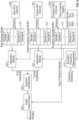
- FIG. 4 depicts a flow diagram of a method 400 for determining resolver position according to one or more embodiments described herein.
- the method 400 performs feedback sample data acquisition using zero crossing points and quadrant identification using the excitation signal.
- Cosine ADC channel 401, sine ADC channel 402, and excitation ADC channel 403 feed buffers 411, 412, 413 respectively with sample data acquired from the feedback signals.
- the buffers 411-413 are circular buffers, although other types of buffers can be implemented.
- the sample data acquired by the excitation ADC channel 403 can also feed an excitation frequency measurement block 414 that outputs a frequency monitoring signal.
- a first integration module 421 uses the zero crossing triggers from the excitation ADC channel 403 and sample data from the buffer 411 to determine a cosine amplitude.
- a second integration module 422 uses the zero crossing triggers from the excitation ADC channel 403 and sample data from the buffer 412 to determine a sine amplitude.
- a quadrant identification block 424 determines, based on the sine amplitude and the cosine amplitude, a quadrant of the resolver (see, e.g., FIGS. 1A-1C ).
- An angle determination module 426 uses the identified quadrant to determine a resolver position.
- the excitation frequency measurement 414, the integration module 421, the integration module 422, the quadrant identification 424, and/or the angle calculation 426 can be implemented as instructions stored on a computer-readable storage medium, as hardware modules, as special-purpose hardware (e.g., application specific hardware, application specific integrated circuits (ASICs), application specific special processors (ASSPs), field programmable gate arrays (FPGAs), as embedded controllers, hardwired circuitry, etc.), or as some combination or combinations of these.
- ASICs application specific integrated circuits
- ASSPs application specific special processors
- FPGAs field programmable gate arrays
- embedded controllers hardwired circuitry, etc.
- one or more of the components described herein can be a combination of hardware and programming.
- the programming can be processor executable instructions stored on a tangible memory, and the hardware can include the processing device for executing those instructions.
- a system memory can store program instructions that when executed by the processing device implement the engines described herein.
- Other engines can also be utilized to include other
- FIG. 5 depicts a flow diagram of a method 500 for performing integral demodulation using a zero crossing point of the excitation signal according to one or more embodiments described herein.
- the method starts at block 501 and proceeds to decision block 502, where it is determined (such as by the DSP 200 and/or one or more of the ADCs 201-203) whether a zero crossing is detected. This determination repeats until a zero crossing is detected at which point the method 500 proceeds to blocks 503, 504, 505.
- excitation signal samples are acquired, such as for a half period.
- sine signal samples are acquired, such as for a half period.
- cosine signal samples are acquired, such as for a half period.
- the method 500 proceeds to block 506, where values for "index1," "sinesum,” and "cosine sum" are set to zero.
- the method 500 proceeds to decision block 507 where it is determined whether the excitation sample midpoint is positive (i.e., greater than zero). If it is determined at decision block 507 that the excitation sample midpoint is positive, the method 500 proceeds to decision block 508, where it is determined whether the index (e.g., "index1" from block 506) is less than a value n. If so, the method 500 proceeds to blocks 509 and 510. At block 509, a value Sinesum is set to a previous Sinesum value plus a sine sample for the current index. Similarly, at block 510, a value Cosinesum is set to a previous Cosinesum value plus a cosine sample for the current index. After blocks 509, 510, the method 500 proceeds to block 511 where the index is incremented and the method 500 returns to decision block 508.
- the index e.g., "index1" from block 506
- the method 500 proceeds to decision block 512, where it is determined whether the index (e.g., "index1" from block 506) is less than a value n. If so, the method 500 proceeds to blocks 513 and 514.
- a value Sinesum is set to the negative (opposite) of a quantity represented by a previous Sinesum value plus a sine sample for the current index.
- a value Cosinesum is set to the negative (opposite) of a quantity represented by a previous Cosinesum value plus a cosine sample for the current index.
- the method 500 proceeds to block 515 where the index is incremented and the method 500 returns to decision block 512.
- the method 500 proceeds to block 512 where the SineSum and CosineSum values are calculated, respectively, by doubling the previous SineSum and CosineSum values.
- the position is determined using the SineSum and CosineSum values from block 516.
- the position is determined using the arctan of the SineSum and CosineSum values from block 516.
- the method 500 then ends at block 518.
- the excitation signal is sinusoidal, which has three zero crossing points per full cycle; hence, the signal frequency can be calculated as the number of zero crossing points per second divided by three.
- One or more embodiments described herein also provide improved accuracy.
- each of the resolver signals excitation, sine and cosine
- At least one sample delay is introduced between the samples and hence the sine to cosine ratio is not accurately represented.
- one or more embodiments described herein sample the three resolver signals simultaneously using three ADCs that are in-built to processor (e.g., DSP).
- processors are running in Mhz frequency, the phase delay between the signals will only be the order of microseconds. Hence the sine to cosine ratio is accurately represented.
- One or more embodiments described herein also provide improved processor (e.g., DSP) utilization.
- DSP digital signal processor
- To calculate the amplitude conventional approaches process samples for a full period of the signal which is time consuming. Also such approaches use each excitation sample to identify the quadrant of sine and cosine feedback signals.
- one or more embodiments described herein collect samples from a zero crossing point such that samples only for a half period need to be integrated, and the integral output is multiplied by two to get the amplitude. Also the quadrant of the sine and cosine can be identified using only the sign of excitation signal that corresponds to the midpoint value of the excitation signal.
- the present embodiments may be a system, a method, and/or a computer program product at any possible technical detail level of integration
- the computer program product may include a computer readable storage medium (or media) having computer readable program instructions thereon for causing a processor to carry out aspects of the present disclosure
- each block in the flowchart or block diagrams may represent a module, segment, or portion of instructions, which comprises one or more executable instructions for implementing the specified logical function(s).
- the functions noted in the blocks may occur out of the order noted in the Figures.
- two blocks shown in succession may, in fact, be executed substantially concurrently, or the blocks may sometimes be executed in the reverse order, depending upon the functionality involved.
Landscapes
- Engineering & Computer Science (AREA)
- Computer Networks & Wireless Communication (AREA)
- Signal Processing (AREA)
- Power Engineering (AREA)
- Physics & Mathematics (AREA)
- General Physics & Mathematics (AREA)
- Transmission And Conversion Of Sensor Element Output (AREA)
Abstract
Description
- The subject matter disclosed herein generally relates to signal processing and, more particularly, to resolver integral demodulation using zero crossing points.
- A resolver, also referred to as a motor resolver, is an electrical transformer that measures angle of rotation. Resolvers are made up of a rotor and a stator. The rotor is mounted on a shaft of a device (e.g., motor, turbine engine, etc.) to be monitored, for example. The stator includes multiple transformers (also referred to as "windings"), for example, an input transformer and two output transformers. As an input signal (also referred to as a "reference" signal or an "excitation" signal) is applied to the input transformer, one of the output transformers generates a sine output and the other of the output transformers generates a cosine output.
- In one exemplary embodiment, a method is provided. The method includes storing, in a first buffer associated with a first analog to digital converter (ADC) of a digital signal processor (DSP), resolver sine values collected from a first resolver, a second resolver, and a third resolver. The method further includes storing, in a second buffer associated with a second ADC of the DSP, resolver cosine values collected from the first resolver, the second resolver, and the third resolver. The method further includes storing, in a third buffer associated with a third ADC of the DSP, resolver excitation values collected from the first resolver, the second resolver, and the third resolver. The method further includes determining a midpoint value of the resolver excitation values. The method further includes determining a sine amplitude based at least in part on the resolver sine values and the midpoint value. The method further includes determining a cosine amplitude based at least in part on the resolver sine values and the midpoint value. The method further includes identifying a quadrant of a resolver position.
- In addition to one or more of the features described herein, or as an alternative, further embodiments of the method may include determining a quadrant position based at least in part on the quadrant.
- In addition to one or more of the features described herein, or as an alternative, further embodiments of the method may include that the resolver sine values, the resolver cosine values, and the resolver excitation values are collected simultaneously.
- In addition to one or more of the features described herein, or as an alternative, further embodiments of the method may include that the resolver sine values, the resolver cosine values, and the resolver excitation values are collected relative to a zero crossing.
- In addition to one or more of the features described herein, or as an alternative, further embodiments of the method may include that the resolver sine values, the resolver cosine values, and the resolver excitation values are collected relative to a zero crossing for a half period.
- In addition to one or more of the features described herein, or as an alternative, further embodiments of the method may include that identifying the quadrant of the resolver position includes doubling the sine amplitude and the cosine amplitude.
- In addition to one or more of the features described herein, or as an alternative, further embodiments of the method may include that identifying the quadrant is based on a sign of an excitation signal applied to the first resolver, the second resolver, and the third resolver.
- In addition to one or more of the features described herein, or as an alternative, further embodiments of the method may include that the first buffer is a first circular buffer, wherein the second buffer is a second circular buffer, and wherein the third buffer is a third circular buffer.
- In another exemplary embodiment a digital signal processor (DSP) includes a first analog to digital converter (ADC) having a first buffer associated therewith, the first buffer storing resolver sine values collected from a first resolver, a second resolver, and a third resolver. The DSP further includes a second ADC having a second buffer associated therewith, the second buffer storing resolver cosine values collected from the first resolver, the second resolver, and the third resolver. The DSP further includes a third ADC having a third buffer associated therewith, the third buffer storing resolver excitation values collected from the first resolver, the second resolver, and the third resolver. The DSP further includes a first integrator to determine a sine amplitude based at least in part on the resolver sine values and a midpoint of a resolver excitation signal. The DSP further includes a second integrator to determine a cosine amplitude based at least in part on the resolver cosine values and the midpoint of the resolver excitation signal. The DSP further includes a quadrant identifier to identifies a quadrant of a resolver position based at least in part on the sine amplitude and the cosine amplitude.
- In addition to one or more of the features described herein, or as an alternative, further embodiments of the DSP may include an angle determining module to determine a quadrant position based at least in part on the quadrant.
- In addition to one or more of the features described herein, or as an alternative, further embodiments of the DSP may include that the resolver sine values, the resolver cosine values, and the resolver excitation values are collected simultaneously.
- In addition to one or more of the features described herein, or as an alternative, further embodiments of the DSP may include that the resolver sine values, the resolver cosine values, and the resolver excitation values are collected relative to a zero crossing.
- In addition to one or more of the features described herein, or as an alternative, further embodiments of the DSP may include that the resolver sine values, the resolver cosine values, and the resolver excitation values are collected relative to a zero crossing for a half period.
- In addition to one or more of the features described herein, or as an alternative, further embodiments of the DSP may include that identifying the quadrant of the resolver position includes doubling the sine amplitude and the cosine amplitude.
- In addition to one or more of the features described herein, or as an alternative, further embodiments of the DSP may include that the quadrant identifier identifies the quadrant based on a sign of an excitation signal applied to the first resolver, the second resolver, and the third resolver.
- In addition to one or more of the features described herein, or as an alternative, further embodiments of the DSP may include that the first buffer is a first circular buffer, wherein the second buffer is a second circular buffer, and wherein the third buffer is a third circular buffer.
- Other embodiments described herein implement features of the above-described method in computer systems and computer program products.
- The above features and advantages, and other features and advantages, of the disclosure are readily apparent from the following detailed description when taken in connection with the accompanying drawings.
- The foregoing and other features, and advantages of the present disclosure are apparent from the following detailed description taken in conjunction with the accompanying drawings in which:
-
FIGS. 1A-1C show the resolver quadrants and the sign of the feedback signals in each quadrant according to one or more embodiments described herein; -
FIG. 2 depicts an example of a digital signal processor that includes three analog to digital converters according to one or more embodiments described herein; -
FIG. 3 depicts a flow diagram of a method for determining resolver position according to one or more embodiments described herein; -
FIG. 4 depicts a flow diagram of a method for determining resolver position according to one or more embodiments described herein; and -
FIG. 5 depicts a flow diagram of a method for performing integral demodulation using a zero crossing point of the excitation signal according to one or more embodiments described herein. - For the purposes of promoting an understanding of the principles of the present disclosure, reference will now be made to the embodiments illustrated in the drawings, and specific language will be used to describe the same. It will nevertheless be understood that no limitation of the scope of this disclosure is thereby intended. The following description is merely illustrative in nature and is not intended to limit the present disclosure, its application or uses. It should be understood that throughout the drawings, corresponding reference numerals indicate like or corresponding parts and features. As used herein, the term controller refers to processing circuitry that may include an application specific integrated circuit (ASIC), an electronic circuit, an electronic processor (shared, dedicated, or group) and memory that executes one or more software or firmware programs, a combinational logic circuit, and/or other suitable interfaces and components that provide the described functionality.
- Additionally, the term "exemplary" is used herein to mean "serving as an example, instance or illustration." Any embodiment or design described herein as "exemplary" is not necessarily to be construed as preferred or advantageous over other embodiments or designs. The terms "at least one" and "one or more" are understood to include any integer number greater than or equal to one, i.e. one, two, three, four, etc. The terms "a plurality" are understood to include any integer number greater than or equal to two, i.e. two, three, four, five, etc. The term "connection" can include an indirect "connection" and a direct "connection."
- Turning to an overview of technologies that are more specifically relevant to aspects of the present disclosure, a resolver or multiple resolvers can be used to measure rotation, such as of a motor, turbine engine, etc. In some cases, three resolvers may be used. Resolvers are excited with an excitation signal. The resolver provides three analog feedback signals, which take the form of sinusoids, as follows: the excitation signal, a sine signal, and a cosine signal. Demodulation of the resolver sine and cosine signals is utilized in many signal processing applications. In the demodulation of the resolver sine and cosine signals, a quadrant of the resolver position is determined based on the signs of the excitation, sine, and cosine signals.
FIGS. 1A-1C show the resolver quadrants and the sign of the feedback signals in each quadrant. Particularly,FIG. 1A depicts agraphical representation 100 of resolver signals phase relationships across four quadrants.FIG. 1B depicts agraphical representation 110 of resolver signals phase relationships across four quadrants where the amplitude of the excitation signal is positive (i.e., greater than zero).FIG. 1C depicts agraphical representation 120 of resolver signals phase relationships across four quadrants where the amplitude of the excitation signal is negative (i.e., less than zero). - Many existing demodulation algorithms for determining a quadrant of the resolver position are time consuming, resource intensive, and/or inaccurate. Conventionally, the feedback signals are fed into the three separate analog to digital converters (ADCs), and the digitally converted data from the ADCs is fed into a digital signal processor (DSP). More particularly, resolver feedback signals sample data are collected into buffers, such as one buffer per resolver (e.g., three buffers for three resolvers): one for the excitation signal (ExcitationRAMBuffer), one for sine signal (SineRAMBuffer), and one for cosine signal (CosineRAMBuffer). These buffers are used to demodulate the feedback signals and determine the rotational position of the resolver. Once a required number of samples are collected, the resolver signal demodulation is performed using an integral demodulation algorithm. The integral demodulation is performed by integrating at least one full period of the sine and cosine feedback samples rectified about their respective midpoints and calculating the angular position using trigonometric relationships and the excitation reference to determine the quadrant of the angular position. This approach has several disadvantages. First, to determine a more accurate resolver position, each of the three feedback signals must be sampled simultaneously; however, conventional approaches acquire the three feedback signals using three different ADCs. This results in a phase delay of minimum one sample and hence produces less accurate results. Second, this approach uses more processing time/resources for the integral demodulation and quadrant determination because the resolver signals integration is done for the full period of the feedback signals and because each excitation sample is compared to identify the quadrant information.
- One or more embodiments described herein address these and other shortcomings by implementing a DSP with internal ADCs for each of the three resolver feedback signals (e.g., excitation, sine, and cosine) simultaneously.
FIG. 2 depicts an example of adigital signal processor 200 that includes three ADCs:ADC 1 201,ADC2 202, andADC3 203. In this example, each of the ADCs 201-203 receive respective cosine, sine, and excitation signals fromresolvers 210, which may represent multiple (e.g., three) resolvers. For example, theADC1 201 receives resolver cosine signals 211 from the resolvers 210 (e.g., resolver1 cosine, resolver2 cosine, and resolver3 cosine); theADC2 202 receives resolver sine signals 212 from the resolvers 210 (e.g., resolver1 sine, resolver2 sine, and resolver3 sine); and theADC3 203 receives resolver excitation signals 213 from the resolvers 210 (e.g., resolver1 excitation, resolver2 excitation, and resolver3 excitation). Each of the ADCs 201-203 includes an integral or associated buffer (e.g., a random access memory (RAM) buffer) for storing sample data from the feedback signals, and the DSP is capable of detecting zero crossings for the feedback signals. This is shown inFIG. 3 , which is now described. - Particularly,
FIG. 3 depicts a flow diagram of amethod 300 for determining resolver position according to one or more embodiments described herein. InFIG. 3 , each of the buffers are shown. Particularly, a cosine RAM buffer 301 (associated with the ADC1 201) stores resolver cosine sample data, a sine RAM buffer 302 (associated with the ADC2 202) stores resolver sine sample data, and an excitation RAM buffer 303 (associated with the ADC3 203) stores resolver excitation sample data. - Data from the
cosine RAM buffer 301 is fed into a first integral demodulation andquadrant identification block 311 along with a sign of a midpoint of a sample from theexcitation RAM buffer 303. The first integral demodulation andquadrant identification block 311 determines and outputs a cosine amplitude into an angle calculation block 320. - Similarly, data from the
sine RAM buffer 302 is fed into a second integral demodulation andquadrant identification block 312 along with the sign of a midpoint of a sample from theexcitation RAM buffer 303. The second integral demodulation andquadrant identification block 312 determines and outputs a sine amplitude into the angle calculation block 320. - More particularly, the first and second integral demodulation and quadrant identification blocks 311, 312 respectively integrate half periods of the cosine and sine feedback samples. Once a threshold number of samples are collected, resolver signal demodulation is performed using an integral demodulation approach. Pseudcode of an example of such an integral demodulation approach is as follows:
               if (excBuffer[midpoint] > MidpointADC):
                      For each sample (i) in numSamples:
                      sinSum += (sinBuffer[i] )
                       cosSum += (cosBuffer[i])
               else:
                      For each sample (i) in numSamples:
                      sinSum += (- sinBuffer[i])
                       cosSum += (- cosBuffer[i])
               SineSum = 2 X SineSum
               CosineSum = 2 X CosineSum
Claims (15)
- A method comprising:storing, in a first buffer associated with a first analog to digital converter, ADC, of a digital signal processor, DSP, resolver sine values collected from a first resolver, a second resolver, and a third resolver;storing, in a second buffer associated with a second ADC of the DSP, resolver cosine values collected from the first resolver, the second resolver, and the third resolver;storing, in a third buffer associated with a third ADC of the DSP, resolver excitation values collected from the first resolver, the second resolver, and the third resolver;determining a midpoint value of the resolver excitation values;determining a sine amplitude based at least in part on the resolver sine values and the midpoint value;determining a cosine amplitude based at least in part on the resolver sine values and the midpoint value; andidentifying a quadrant of a resolver position.
- The method of claim 1, further comprising determining a quadrant position based at least in part on the quadrant.
- The method of claim 1 or 2, wherein the resolver sine values, the resolver cosine values, and the resolver excitation values are collected simultaneously.
- The method of claim 1, 2 or 3, wherein the resolver sine values, the resolver cosine values, and the resolver excitation values are collected relative to a zero crossing.
- The method of any preceding claim, wherein the resolver sine values, the resolver cosine values, and the resolver excitation values are collected relative to a zero crossing for a half period.
- The method of any preceding claim, wherein identifying the quadrant of the resolver position comprises doubling the sine amplitude and the cosine amplitude.
- The method of any preceding claim, wherein identifying the quadrant is based on a sign of an excitation signal applied to the first resolver, the second resolver, and the third resolver.
- The method of any preceding claim, wherein the first buffer is a first circular buffer, wherein the second buffer is a second circular buffer, and wherein the third buffer is a third circular buffer.
- A digital signal processor, DSP, comprising:a first analog to digital converter, ADC, (201) having a first buffer (301) associated therewith, the first buffer storing resolver sine values collected from a first resolver, a second resolver, and a third resolver;a second ADC (202) having a second buffer (302) associated therewith, the second buffer storing resolver cosine values collected from the first resolver, the second resolver, and the third resolver;a third ADC (203) having a third buffer (303) associated therewith, the third buffer storing resolver excitation values collected from the first resolver, the second resolver, and the third resolver;a first integrator to determine a sine amplitude based at least in part on the resolver sine values and a midpoint of a resolver excitation signal;a second integrator to determine a cosine amplitude based at least in part on the resolver cosine values and the midpoint of the resolver excitation signal; anda quadrant identifier to identifies a quadrant of a resolver position based at least in part on the sine amplitude and the cosine amplitude.
- The DSP of claim 9, further comprising an angle determining module (426) to determine a quadrant position based at least in part on the quadrant.
- The DSP of claim 9 or 10, wherein the resolver sine values, the resolver cosine values, and the resolver excitation values are collected simultaneously.
- The DSP of claim 9, 10 or 11, wherein the resolver sine values, the resolver cosine values, and the resolver excitation values are collected relative to a zero crossing.
- The DSP of any of claims 9 to 12, wherein the resolver sine values, the resolver cosine values, and the resolver excitation values are collected relative to a zero crossing for a half period.
- The DSP of any of claims 9 to 13, wherein identifying the quadrant of the resolver position comprises doubling the sine amplitude and the cosine amplitude.
- The DSP of any of claims 9 to 14, wherein the quadrant identifier identifies the quadrant based on a sign of an excitation signal applied to the first resolver, the second resolver, and the third resolver; and/or, wherein the first buffer (301) is a first circular buffer, wherein the second buffer (302) is a second circular buffer, and wherein the third buffer (303) is a third circular buffer.
Applications Claiming Priority (1)
| Application Number | Priority Date | Filing Date | Title |
|---|---|---|---|
| IN202211027653 | 2022-05-13 |
Publications (2)
| Publication Number | Publication Date |
|---|---|
| EP4276417A1 true EP4276417A1 (en) | 2023-11-15 |
| EP4276417B1 EP4276417B1 (en) | 2025-04-09 |
Family
ID=86328771
Family Applications (1)
| Application Number | Title | Priority Date | Filing Date |
|---|---|---|---|
| EP23171329.8A Active EP4276417B1 (en) | 2022-05-13 | 2023-05-03 | Resolver integral demodulation using zero crossing points |
Country Status (4)
| Country | Link |
|---|---|
| US (1) | US11722343B1 (en) |
| EP (1) | EP4276417B1 (en) |
| BR (1) | BR102023009162A2 (en) |
| CA (1) | CA3198929A1 (en) |
Families Citing this family (1)
| Publication number | Priority date | Publication date | Assignee | Title |
|---|---|---|---|---|
| US12388461B2 (en) * | 2023-03-16 | 2025-08-12 | Hamilton Sundstrand Corporation | Timer-based resolver integral demodulation |
Citations (4)
| Publication number | Priority date | Publication date | Assignee | Title |
|---|---|---|---|---|
| JP2008273478A (en) * | 2007-05-07 | 2008-11-13 | Mitsubishi Electric Corp | Electric power steering control device |
| US20160102996A1 (en) * | 2014-10-14 | 2016-04-14 | Qatar University | Phase-locked loop (pll)-type resolver/converter method and apparatus |
| US20180205391A1 (en) * | 2017-01-18 | 2018-07-19 | Raytheon Company | Resolver to digital conversion apparatus and method |
| US20180323797A1 (en) * | 2015-01-29 | 2018-11-08 | Renesas Electronics Corporation | Semiconductor Device |
Family Cites Families (6)
| Publication number | Priority date | Publication date | Assignee | Title |
|---|---|---|---|---|
| JP2005061943A (en) | 2003-08-11 | 2005-03-10 | Minebea Co Ltd | Variable reluctance type resolver |
| US7298967B2 (en) | 2005-04-21 | 2007-11-20 | Delphi Technologies, Inc. | Electromagnetic sensor direct communication algorithm to a digital microprocessor |
| JP4949943B2 (en) | 2007-06-18 | 2012-06-13 | 愛三工業株式会社 | Resolver |
| ES2811533T3 (en) | 2012-03-05 | 2021-03-12 | Novanta Corp | Phase estimation method and apparatus for it |
| US11092464B2 (en) | 2019-01-14 | 2021-08-17 | Hamilton Sundstrand Corporation | High speed AC input sensor conversion |
| US11177987B1 (en) * | 2020-10-27 | 2021-11-16 | Infineon Technologies Ag | Resolver signal processing |
-
2022
- 2022-07-08 US US17/860,633 patent/US11722343B1/en active Active
-
2023
- 2023-05-03 EP EP23171329.8A patent/EP4276417B1/en active Active
- 2023-05-05 CA CA3198929A patent/CA3198929A1/en active Pending
- 2023-05-12 BR BR102023009162-8A patent/BR102023009162A2/en unknown
Patent Citations (4)
| Publication number | Priority date | Publication date | Assignee | Title |
|---|---|---|---|---|
| JP2008273478A (en) * | 2007-05-07 | 2008-11-13 | Mitsubishi Electric Corp | Electric power steering control device |
| US20160102996A1 (en) * | 2014-10-14 | 2016-04-14 | Qatar University | Phase-locked loop (pll)-type resolver/converter method and apparatus |
| US20180323797A1 (en) * | 2015-01-29 | 2018-11-08 | Renesas Electronics Corporation | Semiconductor Device |
| US20180205391A1 (en) * | 2017-01-18 | 2018-07-19 | Raytheon Company | Resolver to digital conversion apparatus and method |
Also Published As
| Publication number | Publication date |
|---|---|
| CA3198929A1 (en) | 2023-11-13 |
| US11722343B1 (en) | 2023-08-08 |
| EP4276417B1 (en) | 2025-04-09 |
| BR102023009162A2 (en) | 2023-11-14 |
Similar Documents
| Publication | Publication Date | Title |
|---|---|---|
| EP0978947B1 (en) | Resolver signal processing system | |
| US9857203B2 (en) | Resolver device | |
| JPS62162968A (en) | speed detection device | |
| US20100315075A1 (en) | Resolver of phase difference type | |
| US4621224A (en) | Position/speed detection method and apparatus | |
| EP4276417B1 (en) | Resolver integral demodulation using zero crossing points | |
| CN108375391A (en) | Cosine and sine signal processing method and system | |
| JP2003014440A (en) | Position detection device | |
| US9140581B2 (en) | Position detector | |
| EP4431879A1 (en) | Timer-based resolver integral demodulation | |
| JPS61137011A (en) | Method for enhancing output accuracy of encoder | |
| JP4119460B2 (en) | Encoder output signal amplitude calculation device and encoder output signal amplitude calculation program | |
| JP3092100B2 (en) | Position detector with error correction function | |
| WO2019017042A1 (en) | Rotation angle sensor-digital converter and rotation angle sensor-digital conversion method | |
| CN114397496A (en) | Phase measurement method, system and medium applied to voltage and current of standard meter | |
| US12460948B2 (en) | Resolver quadrant detection | |
| JPH0529045B2 (en) | ||
| JPH0449892B2 (en) | ||
| KR20020058908A (en) | Apparatus and method for high resolution processing of encoder signal for a motor control | |
| CN114778884B (en) | Speed measurement method, device and electronic equipment based on incremental encoder | |
| US20250377223A1 (en) | Real-time synchronization technique for rectification of resolver feedbacks | |
| JP4227352B2 (en) | Coincidence detection apparatus and method | |
| Han et al. | Resolver-to-digital converter based on tangent algorithm | |
| CN121954069A (en) | CPLD-based sine and cosine encoder decoding methods, equipment, and media | |
| BR102024003284A2 (en) | METHOD FOR DETERMINING A LOCATION OF A RESOLVER, AND DIGITAL SIGNAL PROCESSING SYSTEM FOR DETERMINING A POSITION OF A RESOLVER |
Legal Events
| Date | Code | Title | Description |
|---|---|---|---|
| PUAI | Public reference made under article 153(3) epc to a published international application that has entered the european phase |
Free format text: ORIGINAL CODE: 0009012 |
|
| STAA | Information on the status of an ep patent application or granted ep patent |
Free format text: STATUS: THE APPLICATION HAS BEEN PUBLISHED |
|
| AK | Designated contracting states |
Kind code of ref document: A1 Designated state(s): AL AT BE BG CH CY CZ DE DK EE ES FI FR GB GR HR HU IE IS IT LI LT LU LV MC ME MK MT NL NO PL PT RO RS SE SI SK SM TR |
|
| STAA | Information on the status of an ep patent application or granted ep patent |
Free format text: STATUS: REQUEST FOR EXAMINATION WAS MADE |
|
| 17P | Request for examination filed |
Effective date: 20240515 |
|
| RBV | Designated contracting states (corrected) |
Designated state(s): AL AT BE BG CH CY CZ DE DK EE ES FI FR GB GR HR HU IE IS IT LI LT LU LV MC ME MK MT NL NO PL PT RO RS SE SI SK SM TR |
|
| GRAP | Despatch of communication of intention to grant a patent |
Free format text: ORIGINAL CODE: EPIDOSNIGR1 |
|
| STAA | Information on the status of an ep patent application or granted ep patent |
Free format text: STATUS: GRANT OF PATENT IS INTENDED |
|
| RIC1 | Information provided on ipc code assigned before grant |
Ipc: H04L 27/06 20060101ALI20241106BHEP Ipc: G01D 5/20 20060101AFI20241106BHEP |
|
| INTG | Intention to grant announced |
Effective date: 20241115 |
|
| GRAS | Grant fee paid |
Free format text: ORIGINAL CODE: EPIDOSNIGR3 |
|
| GRAA | (expected) grant |
Free format text: ORIGINAL CODE: 0009210 |
|
| STAA | Information on the status of an ep patent application or granted ep patent |
Free format text: STATUS: THE PATENT HAS BEEN GRANTED |
|
| AK | Designated contracting states |
Kind code of ref document: B1 Designated state(s): AL AT BE BG CH CY CZ DE DK EE ES FI FR GB GR HR HU IE IS IT LI LT LU LV MC ME MK MT NL NO PL PT RO RS SE SI SK SM TR |
|
| REG | Reference to a national code |
Ref country code: GB Ref legal event code: FG4D |
|
| REG | Reference to a national code |
Ref country code: CH Ref legal event code: EP |
|
| REG | Reference to a national code |
Ref country code: DE Ref legal event code: R096 Ref document number: 602023002791 Country of ref document: DE |
|
| REG | Reference to a national code |
Ref country code: IE Ref legal event code: FG4D |
|
| PGFP | Annual fee paid to national office [announced via postgrant information from national office to epo] |
Ref country code: DE Payment date: 20250423 Year of fee payment: 3 |
|
| PGFP | Annual fee paid to national office [announced via postgrant information from national office to epo] |
Ref country code: IT Payment date: 20250531 Year of fee payment: 3 |
|
| PGFP | Annual fee paid to national office [announced via postgrant information from national office to epo] |
Ref country code: FR Payment date: 20250520 Year of fee payment: 3 |
|
| PGFP | Annual fee paid to national office [announced via postgrant information from national office to epo] |
Ref country code: AT Payment date: 20250721 Year of fee payment: 3 |
|
| REG | Reference to a national code |
Ref country code: NL Ref legal event code: MP Effective date: 20250409 |
|
| PG25 | Lapsed in a contracting state [announced via postgrant information from national office to epo] |
Ref country code: NL Free format text: LAPSE BECAUSE OF FAILURE TO SUBMIT A TRANSLATION OF THE DESCRIPTION OR TO PAY THE FEE WITHIN THE PRESCRIBED TIME-LIMIT Effective date: 20250409 |
|
| REG | Reference to a national code |
Ref country code: AT Ref legal event code: MK05 Ref document number: 1783877 Country of ref document: AT Kind code of ref document: T Effective date: 20250409 |
|
| PG25 | Lapsed in a contracting state [announced via postgrant information from national office to epo] |
Ref country code: FI Free format text: LAPSE BECAUSE OF FAILURE TO SUBMIT A TRANSLATION OF THE DESCRIPTION OR TO PAY THE FEE WITHIN THE PRESCRIBED TIME-LIMIT Effective date: 20250409 Ref country code: PT Free format text: LAPSE BECAUSE OF FAILURE TO SUBMIT A TRANSLATION OF THE DESCRIPTION OR TO PAY THE FEE WITHIN THE PRESCRIBED TIME-LIMIT Effective date: 20250811 Ref country code: ES Free format text: LAPSE BECAUSE OF FAILURE TO SUBMIT A TRANSLATION OF THE DESCRIPTION OR TO PAY THE FEE WITHIN THE PRESCRIBED TIME-LIMIT Effective date: 20250409 |
|
| REG | Reference to a national code |
Ref country code: LT Ref legal event code: MG9D |
|
| PG25 | Lapsed in a contracting state [announced via postgrant information from national office to epo] |
Ref country code: GR Free format text: LAPSE BECAUSE OF FAILURE TO SUBMIT A TRANSLATION OF THE DESCRIPTION OR TO PAY THE FEE WITHIN THE PRESCRIBED TIME-LIMIT Effective date: 20250710 Ref country code: NO Free format text: LAPSE BECAUSE OF FAILURE TO SUBMIT A TRANSLATION OF THE DESCRIPTION OR TO PAY THE FEE WITHIN THE PRESCRIBED TIME-LIMIT Effective date: 20250709 |
|
| PG25 | Lapsed in a contracting state [announced via postgrant information from national office to epo] |
Ref country code: PL Free format text: LAPSE BECAUSE OF FAILURE TO SUBMIT A TRANSLATION OF THE DESCRIPTION OR TO PAY THE FEE WITHIN THE PRESCRIBED TIME-LIMIT Effective date: 20250409 |
|
| PG25 | Lapsed in a contracting state [announced via postgrant information from national office to epo] |
Ref country code: BG Free format text: LAPSE BECAUSE OF FAILURE TO SUBMIT A TRANSLATION OF THE DESCRIPTION OR TO PAY THE FEE WITHIN THE PRESCRIBED TIME-LIMIT Effective date: 20250409 |
|
| PG25 | Lapsed in a contracting state [announced via postgrant information from national office to epo] |
Ref country code: HR Free format text: LAPSE BECAUSE OF FAILURE TO SUBMIT A TRANSLATION OF THE DESCRIPTION OR TO PAY THE FEE WITHIN THE PRESCRIBED TIME-LIMIT Effective date: 20250409 |
|
| PG25 | Lapsed in a contracting state [announced via postgrant information from national office to epo] |
Ref country code: AT Free format text: LAPSE BECAUSE OF FAILURE TO SUBMIT A TRANSLATION OF THE DESCRIPTION OR TO PAY THE FEE WITHIN THE PRESCRIBED TIME-LIMIT Effective date: 20250409 |
|
| PG25 | Lapsed in a contracting state [announced via postgrant information from national office to epo] |
Ref country code: RS Free format text: LAPSE BECAUSE OF FAILURE TO SUBMIT A TRANSLATION OF THE DESCRIPTION OR TO PAY THE FEE WITHIN THE PRESCRIBED TIME-LIMIT Effective date: 20250709 |
|
| PG25 | Lapsed in a contracting state [announced via postgrant information from national office to epo] |
Ref country code: IS Free format text: LAPSE BECAUSE OF FAILURE TO SUBMIT A TRANSLATION OF THE DESCRIPTION OR TO PAY THE FEE WITHIN THE PRESCRIBED TIME-LIMIT Effective date: 20250809 |
|
| PG25 | Lapsed in a contracting state [announced via postgrant information from national office to epo] |
Ref country code: LV Free format text: LAPSE BECAUSE OF FAILURE TO SUBMIT A TRANSLATION OF THE DESCRIPTION OR TO PAY THE FEE WITHIN THE PRESCRIBED TIME-LIMIT Effective date: 20250409 |
|
| REG | Reference to a national code |
Ref country code: DE Ref legal event code: R097 Ref document number: 602023002791 Country of ref document: DE |
|
| PG25 | Lapsed in a contracting state [announced via postgrant information from national office to epo] |
Ref country code: DK Free format text: LAPSE BECAUSE OF FAILURE TO SUBMIT A TRANSLATION OF THE DESCRIPTION OR TO PAY THE FEE WITHIN THE PRESCRIBED TIME-LIMIT Effective date: 20250409 Ref country code: SM Free format text: LAPSE BECAUSE OF FAILURE TO SUBMIT A TRANSLATION OF THE DESCRIPTION OR TO PAY THE FEE WITHIN THE PRESCRIBED TIME-LIMIT Effective date: 20250409 |
|
| PG25 | Lapsed in a contracting state [announced via postgrant information from national office to epo] |
Ref country code: LU Free format text: LAPSE BECAUSE OF NON-PAYMENT OF DUE FEES Effective date: 20250503 |
|
| PG25 | Lapsed in a contracting state [announced via postgrant information from national office to epo] |
Ref country code: CZ Free format text: LAPSE BECAUSE OF FAILURE TO SUBMIT A TRANSLATION OF THE DESCRIPTION OR TO PAY THE FEE WITHIN THE PRESCRIBED TIME-LIMIT Effective date: 20250409 |
|
| PG25 | Lapsed in a contracting state [announced via postgrant information from national office to epo] |
Ref country code: EE Free format text: LAPSE BECAUSE OF FAILURE TO SUBMIT A TRANSLATION OF THE DESCRIPTION OR TO PAY THE FEE WITHIN THE PRESCRIBED TIME-LIMIT Effective date: 20250409 |
|
| PG25 | Lapsed in a contracting state [announced via postgrant information from national office to epo] |
Ref country code: SK Free format text: LAPSE BECAUSE OF FAILURE TO SUBMIT A TRANSLATION OF THE DESCRIPTION OR TO PAY THE FEE WITHIN THE PRESCRIBED TIME-LIMIT Effective date: 20250409 |
|
| REG | Reference to a national code |
Ref country code: BE Ref legal event code: MM Effective date: 20250531 |
|
| PG25 | Lapsed in a contracting state [announced via postgrant information from national office to epo] |
Ref country code: MC Free format text: LAPSE BECAUSE OF FAILURE TO SUBMIT A TRANSLATION OF THE DESCRIPTION OR TO PAY THE FEE WITHIN THE PRESCRIBED TIME-LIMIT Effective date: 20250409 |
|
| PLBE | No opposition filed within time limit |
Free format text: ORIGINAL CODE: 0009261 |
|
| STAA | Information on the status of an ep patent application or granted ep patent |
Free format text: STATUS: NO OPPOSITION FILED WITHIN TIME LIMIT |
|
| REG | Reference to a national code |
Ref country code: CH Ref legal event code: L10 Free format text: ST27 STATUS EVENT CODE: U-0-0-L10-L00 (AS PROVIDED BY THE NATIONAL OFFICE) Effective date: 20260218 |
|
| PG25 | Lapsed in a contracting state [announced via postgrant information from national office to epo] |
Ref country code: RO Free format text: LAPSE BECAUSE OF FAILURE TO SUBMIT A TRANSLATION OF THE DESCRIPTION OR TO PAY THE FEE WITHIN THE PRESCRIBED TIME-LIMIT Effective date: 20250409 |
|
| 26N | No opposition filed |
Effective date: 20260112 |
|
| PG25 | Lapsed in a contracting state [announced via postgrant information from national office to epo] |
Ref country code: IE Free format text: LAPSE BECAUSE OF NON-PAYMENT OF DUE FEES Effective date: 20250503 |
|
| PG25 | Lapsed in a contracting state [announced via postgrant information from national office to epo] |
Ref country code: BE Free format text: LAPSE BECAUSE OF NON-PAYMENT OF DUE FEES Effective date: 20250531 |