EP4273749A1 - Voltage limiter for an rfid tag - Google Patents
Voltage limiter for an rfid tag Download PDFInfo
- Publication number
- EP4273749A1 EP4273749A1 EP22171932.1A EP22171932A EP4273749A1 EP 4273749 A1 EP4273749 A1 EP 4273749A1 EP 22171932 A EP22171932 A EP 22171932A EP 4273749 A1 EP4273749 A1 EP 4273749A1
- Authority
- EP
- European Patent Office
- Prior art keywords
- current
- voltage
- sink device
- voltage limiter
- current sink
- Prior art date
- Legal status (The legal status is an assumption and is not a legal conclusion. Google has not performed a legal analysis and makes no representation as to the accuracy of the status listed.)
- Granted
Links
Images




Classifications
-
- H—ELECTRICITY
- H02—GENERATION; CONVERSION OR DISTRIBUTION OF ELECTRIC POWER
- H02H—EMERGENCY PROTECTIVE CIRCUIT ARRANGEMENTS
- H02H9/00—Emergency protective circuit arrangements for limiting excess current or voltage without disconnection
- H02H9/04—Emergency protective circuit arrangements for limiting excess current or voltage without disconnection responsive to excess voltage
-
- G—PHYSICS
- G05—CONTROLLING; REGULATING
- G05F—SYSTEMS FOR REGULATING ELECTRIC OR MAGNETIC VARIABLES
- G05F1/00—Automatic systems in which deviations of an electric quantity from one or more predetermined values are detected at the output of the system and fed back to a device within the system to restore the detected quantity to its predetermined value or values, i.e. retroactive systems
- G05F1/10—Regulating voltage or current
- G05F1/46—Regulating voltage or current wherein the variable actually regulated by the final control device is DC
- G05F1/56—Regulating voltage or current wherein the variable actually regulated by the final control device is DC using semiconductor devices in series with the load as final control devices
- G05F1/575—Regulating voltage or current wherein the variable actually regulated by the final control device is DC using semiconductor devices in series with the load as final control devices characterised by the feedback circuit
-
- G—PHYSICS
- G06—COMPUTING OR CALCULATING; COUNTING
- G06K—GRAPHICAL DATA READING; PRESENTATION OF DATA; RECORD CARRIERS; HANDLING RECORD CARRIERS
- G06K19/00—Record carriers for use with machines and with at least a part designed to carry digital markings
- G06K19/06—Record carriers for use with machines and with at least a part designed to carry digital markings characterised by the kind of the digital marking, e.g. shape, nature, code
- G06K19/067—Record carriers with conductive marks, printed circuits or semiconductor circuit elements, e.g. credit or identity cards also with resonating or responding marks without active components
- G06K19/07—Record carriers with conductive marks, printed circuits or semiconductor circuit elements, e.g. credit or identity cards also with resonating or responding marks without active components with integrated circuit chips
- G06K19/0701—Record carriers with conductive marks, printed circuits or semiconductor circuit elements, e.g. credit or identity cards also with resonating or responding marks without active components with integrated circuit chips at least one of the integrated circuit chips comprising an arrangement for power management
- G06K19/0715—Record carriers with conductive marks, printed circuits or semiconductor circuit elements, e.g. credit or identity cards also with resonating or responding marks without active components with integrated circuit chips at least one of the integrated circuit chips comprising an arrangement for power management the arrangement including means to regulate power transfer to the integrated circuit
-
- G—PHYSICS
- G05—CONTROLLING; REGULATING
- G05F—SYSTEMS FOR REGULATING ELECTRIC OR MAGNETIC VARIABLES
- G05F1/00—Automatic systems in which deviations of an electric quantity from one or more predetermined values are detected at the output of the system and fed back to a device within the system to restore the detected quantity to its predetermined value or values, i.e. retroactive systems
- G05F1/10—Regulating voltage or current
- G05F1/46—Regulating voltage or current wherein the variable actually regulated by the final control device is DC
- G05F1/56—Regulating voltage or current wherein the variable actually regulated by the final control device is DC using semiconductor devices in series with the load as final control devices
- G05F1/565—Regulating voltage or current wherein the variable actually regulated by the final control device is DC using semiconductor devices in series with the load as final control devices sensing a condition of the system or its load in addition to means responsive to deviations in the output of the system, e.g. current, voltage, power factor
Definitions
- the present disclosure relates to a voltage limiter for an RFID tag.
- a voltage limiter for an RFID tag.
- a voltage limiter incorporated in a radio-frequency identification (RFID) integrated circuit (IC) for an RFID tag, for strongly limiting the voltage at the RFID IC at short distances to an RFID reader.
- RFID radio-frequency identification
- RFID tags need to deal with a huge input power range.
- the integrated circuit (IC) of the RFID tag needs to be protected from physical damage. This is typically achieved by including limiter circuitry to limit the input amplitude to a certain maximum level, defined by the physical limitation of the IC process technology.
- a voltage limiter for a radio-frequency identification (RFID) integrated circuit (IC) for an RFID tag the RFID IC including a radio-frequency (RF) rectifier, the voltage limiter comprising:
- the voltage limiter of the present disclosure can more strongly limit the power to the RFID IC under close-coupled conditions to the reader. This addresses a problem in known limiter circuitry of high-power dissipation through the limiter circuitry under near field (high power) conditions which still impacts the performance and lifetime of the RFID tag IC. By strongly limiting the power under close-coupled conditions to the reader, the voltage limiter of the present disclosure may thereby reduce physical damage to the tag IC.
- the voltage limiter of the present disclosure enables an anti-spy feature, to prevent intentional reading of the tag in the near field of the reader, thereby increasing privacy in these conditions.
- This feature guarantees that a tag must be a certain distance from a reader for the tag to be read by that reader, thereby restricting the operating range to a minimum distance.
- the reference voltage is dependent on the output voltage of the RF rectifier. In other embodiments the reference voltage has a predefined value.
- the feedback current may be proportional to the current through the current sink device, for example a multiple or a submultiple of the current through the current sink device.
- the feedback circuitry may comprise a current replica device coupled between the output of the RF rectifier and ground, in parallel with the current sink device.
- the current replica device may be configured such that a current through the current replica device is dependent on the current through the current sink device. For example, the current through the current replica device may increase with increasing current through the current sink device. In some embodiments, the current through the current replica device is substantially proportional to the current through the current sink device, for example a multiple or submultiple.
- Providing a current replica branch in addition to the current sink branch avoids the need to have a diode to mirror the current in the current sink branch, which would limit the sinking capability of the current sink device. For example, if a current mirror were present in the current sink branch, the voltage Vds between the current terminals of the current sink device would be reduced by the voltage Vds between the current terminals of the current mirror.
- the current replica device provides an additional multiplication (division) ratio between the feedback current and the current in the current sink device, ultimately reducing the area of the voltage limiter.
- a control terminal of the current replica device may be coupled to the control terminal of the current sink device.
- the current replica device may be configured to replicate a multiple or submultiple of the current in the current sink device.
- the feedback circuitry may further comprise at least one current mirror for copying the current in the current replica device.
- the current mirror device By copying or mirroring a current in the current replica branch, the current mirror device does not limit the sinking capability of the current sink device.
- At least one current mirror may comprise a current mirror device coupled in series with the current replica device.
- a current terminal of the current mirror device may be coupled to a current terminal of the current replica device, the other current terminal of the current mirror device being coupled to one of ground or the output of the RF rectifier.
- At least one current mirror may comprise a current mirror device and a current copy device, the current copy device having a control terminal coupled to a control terminal of the current mirror device, a first current terminal coupled to a current terminal of the current mirror device, and a second current terminal coupled to the control terminal of the current sink device.
- a current in said current copy device may be proportional to a current in said current replica device.
- Said at least one current mirror may be configured to mirror a multiple or submultiple of the current in the current replica device.
- Said at least one current mirror may comprise a first current mirror for copying the current in the current replica device, and a further current mirror for copying the current in the first current mirror.
- the inclusion of multiple current mirrors in the feedback circuitry may facilitate different ratios between the feedback current and the current in the current sink device, and/or may facilitate providing the feedback current to different circuitry points of the voltage limiter.
- the feedback circuitry may be configured to provide the feedback current to a control terminal of the current sink device.
- the feedback circuitry may be configured to provide the feedback current to a feedback node of the reference generator, wherein a voltage offset is generated between the feedback node and the control terminal of the current sink device.
- This feature may be used to cause the supply voltage to be reduced to a particular voltage level when the rf power is high.
- the voltage may be reduced to a level at which read and write to the tag is not possible.
- the voltage may be reduced to a level which allows read operations only, but no write operations (as a typical example, read functionality requires a minimum of around 0.5V, while write functionality requires a minimum of around .0V).
- This feature may also allow the current sink device to be smaller, by causing it to sink less current at high rf powers.
- the feedback circuitry may comprise an element coupled between the feedback node and the control terminal of the current sink device for generating the voltage offset, the element being a resistor, a diode, a bipolar transistor, or a MOS transistor.
- the current sink device is a main current sink device, the voltage limiter further comprising:
- the supply voltage is reduced to a fixed voltage level when the rf power is high. This prevents the reduced supply voltage from gradually rising as proximity to an RF reader increases further, since higher RF field amplitudes might otherwise raise the supply voltage sufficiently to actuate the RFID IC.
- the value of the fixed voltage level may be selected through the choice of device type for the sense device and additional current sink.
- the main sink device and the additional sink device may be transistors having opposite polarity.
- the sensing device may comprise at least one of an inverter, a Schmitt trigger, a latch, and/or an amplifier which may feature a hysteresis.
- the voltage limiter may further comprise:
- the sensing device may comprise at least one of an inverter, a Schmitt trigger, a latch, and/or an amplifier.
- the sensing device may feature a hysteresis.
- the current sink device is a main current sink device, the voltage limiter further comprising:
- the sensing device may comprise at least one of an inverter, a Schmitt trigger, a latch, and/or an amplifier.
- the sensing device may feature a hysteresis.
- the current sink device may be a transistor having a first polarity, the transistor comprising a control terminal coupled to the output of the reference generator.
- the current replica device may be a transistor having said first polarity.
- the at least one current mirror may comprise a current mirror having a second polarity opposite to said first polarity.
- RFID radio-frequency identification
- IC integrated circuit
- a method for operating a voltage limiter in a radio-frequency identification (RFID) integrated circuit (IC) for an RFID tag the RFID IC including a radio-frequency (RF) rectifier, the method comprising:
- FIG. 1A represents a typical voltage limiter 100, useful for understanding the present invention, the voltage limiter 100 for a radio-frequency identification (RFID) IC of an RFID tag.
- the RFID IC includes a radio-frequency (RF) rectifier (not shown) configured to convert an AC signal received from an antenna (not shown) incorporated in the RFID tag to a DC signal.
- the voltage limiter 100 includes a current sink device 110 coupled between the output (Vrec) 120 of the RF rectifier and a reference or ground potential (gnd) 125, and a reference generator 130 for generating a reference voltage (Vlim) 135 for controlling a current through the current sink device 110 to limit the output voltage of the RF rectifier to a predefined level.
- FIG. 1B conceptually illustrates a voltage limiter 200 according to a first example embodiment of the present disclosure.
- the voltage limiter 200 may be incorporated in an RFID IC of an RFID tag.
- the RFID tag typically includes electronic components to allow the RFID tag to communicate with an external RFID reader, including an RF rectifier (not shown) for generating a DC voltage (Vrec) 230 from an AC signal received from a reader (not shown) through an RFID tag antenna (not shown).
- the voltage limiter 200 includes a current sink device 210 coupled between the output (Vrec) 220 of the RF rectifier and a reference or ground potential (gnd) 225.
- the voltage limiter 200 also includes a reference generator 230 having an output 235 for providing a reference voltage Vlim to the control terminal of the current sink device 210, for controlling a current through the current sink device 210 to limit the output voltage of the RF rectifier Vrec 220 to a predefined voltage level.
- the reference voltage Vlim 235 may be derived by the reference generator 230 from the voltage Vrec 220 output by the RF rectifier.
- the current sink device 210 begins to conduct when the output voltage 220 of the RF rectifier exceeds a predetermined value.
- the reference generator 230 may have a limited driving capability.
- the voltage limiter 200 of this example embodiment also includes feedback circuitry 240, 250 arranged to provide a feedback current to the reference generator 230 to vary the reference voltage Vlim 235 output by the reference generator 230, the feedback current being dependent on the current through the current sink device 210.
- the feedback circuitry 240, 250 includes a current replica device 240, coupled between the output (Vrec) 220 of the RF rectifier and the ground potential 225, in parallel with the current sink device 210.
- the control terminals of the current sink device 210 and the current replica device 240 are connected to each other.
- a current through the replica current device 240 is proportional to the current through the current sink device 210, for example a multiple or a sub-multiple of it.
- the feedback circuitry 240, 250 further comprises elements (represented by path 250) for mirroring and copying the current in the replica current device 240, for example as a multiple or a sub-multiple of it.
- the copied current is connected (sinking or sourcing) to the reference generator 230 to pull current from the reference voltage Vlim in order to influence the voltage Vlim at the output 235 of the reference generator.
- the feedback circuitry 240, 250 thereby provides positive feedback to the reference voltage Vlim 236, the feedback current increasing as the current through the current sink device 210 increases.
- Figure 2 shows a graph illustrating the behaviour of the voltage limiter 200 of the present disclosure and a typical voltage limiter 100.
- the dashed line (b) of Figure 2 shows the voltage Vrec 220 output by the RF rectifier of the RFID tag as a function of the current through the current sink device 210, for the voltage limiter 200 of the first example embodiment described above with reference to Figure 1B .
- the solid line (a) of Figure 2 illustrates the corresponding voltage-current characteristics for a typical voltage limiter without the feedback circuitry described in the present disclosure, such as the voltage limiter 100 shown in Figure 1A .
- this sharp decrease occurs between about 4E-6 and 5E-06A, and the voltage is reduced from about 2.3 V to about 0.5 volts.
- This reduced voltage may gradually increase with further increases to the current, but remains substantially reduced, for example remaining significantly below 1 V.
- the effect of the feedback current in the voltage limiter 200 is thus to automatically reduce the DC voltage supply for the RF tag IC below a predetermined voltage level, for RF field strengths above a predetermined value.
- the level to which the voltage is reduced is dependent on the size of the devices, in particular the current sink device.
- certain functionality of the RFID tag is disabled and can therefore only be used at greater distances from the reader.
- the supply voltage may be reduced below the level at which the memory cannot be written, or even below the level at which the IC cannot be operated.
- both read and write functionality are typically disabled.
- Some or all operations of the tag may therefore be restricted to be performed only above a minimum distance to the reader. Since this feature is not controlled by a digital signal, but by limiting power to the RFID IC, security may be improved.
- Reducing the voltage to the RFID tag IC at high RF powers may also prevent physical damage to the RFID tag IC.
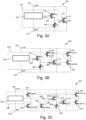
- Figures 3B and 3C schematically illustrate circuits for a voltage limiter 200 according to second and third respective example embodiments.
- Figure 3A illustrates a circuit for a voltage limiter 100, without the feedback circuitry of the present disclosure, useful for understanding the present disclosure.
- Figure 3A shows a voltage limiter 100 including a current sink device 110 in the form of an NMOS transistor coupled between the output Vrec 120 of the rectifier of the RFID tag, and a ground reference 125.
- a reference generator 130 comprises a voltage reference 160 for outputting a voltage Vref 165 dependent upon the rectifier output voltage Vrec, and further comprises a transistor 170 and a resistor 180 coupled in series between the output Vrec 120 of the rectifier and ground 125.
- the control terminal of the transistor 170 is controlled by the voltage Vref 165.
- a reference voltage Vlim 135 for controlling the current sink device 110 is generated at the connection point between the transistor 170 and resistor 180, which is coupled to the control terminal of current sink device 110.
- FIG. 3B illustrates a voltage limiter 200 according to a second example embodiment of the present invention.
- the voltage limiter 200 includes a current sink device 210, in the form of an NMOS transistor, coupled between the output (Vrec) 220 of the RF rectifier and a reference or ground potential (gnd) 225.
- a reference generator 230 has an output 235 providing a reference voltage Vlim 235 which is input to the control terminal (in this embodiment, the gate terminal) of the current sink device 210 for controlling a current through the current sink device 210 to limit the output voltage of the RF rectifier to a predefined voltage level.
- the reference generator 230 comprises a voltage reference 260 for outputting a voltage Vref 265 dependent upon the rectifier output voltage Vrec, and further comprises a transistor m, 270, in the form of a PMOS transistor, and a resistor R, 280 coupled in series between the output Vrec 220 of the rectifier and ground 225.
- the control terminal (in this embodiment, the gate terminal) of the transistor 270 is controlled by the voltage Vref 165 output by the voltage reference.
- the reference voltage Vlim 235 for controlling the current sink device 210 is generated at the connection between the transistor 270 and resistor 280, this connection point being coupled to the control terminal of current sink device 210.
- the reference voltage Vlim increases with the output voltage 220 of the RF rectifier.
- the current sink device 210 sinks current when the reference voltage Vlim 235 exceeds a predetermined value, in this case the threshold voltage of the current sink device 210.
- the voltage limiter 200 of Figure 3B embodiment also includes feedback circuitry 240, 252, 254 arranged to provide a feedback current to the reference generator 230 to vary the reference voltage Vlim 235 output by the reference generator 230 for controlling the current through the current sink device 210, the feedback current being dependent on the current through the current sink device 210.
- the feedback circuitry 240, 252, 254 includes a current replica device 240, a current mirror device 252 and a current copy device 254.
- the current replica device 252 in the form of a NMOS transistor, is coupled in parallel with the current sink device 210, between the output (Vrec) 220 of the RF rectifier and the reference or ground potential 225.
- the control terminal of the current replica device 240 is connected to the control terminal of the current sink device 210.
- a current through the current replica device 240 may be proportional to the current through the current sink device 210, for example a multiple or a sub-multiple of it.
- the current mirror device 252 and a current copy device 254 together form a current mirror for copying the current in the current replica device 240 (for example a multiple or submultiple of it).
- the current mirror device 252 in the form of a PMOS transistor, is coupled in series with the current replica device 240, between the output Vrec 220 of the RF rectifier and the current replica device 240.
- the source terminal of the current mirror device 252 is coupled to Vrec 220, while the gate and drain terminals of the current mirror device 252 are connected to each other and are coupled to the drain terminal of the current replica device 240.
- the copy current device 254, in the form of a PMOS transistor is coupled between the output Vrec 220 of the RF rectifier and the control terminal of the current sink device 210.
- the source terminal of the current copy device 254 is coupled to the Vrec 220
- the drain terminal of the current copy device 254 is coupled to control terminal of the current sink device 210.
- the control terminal of the copy current device 254 is connected to the control terminal of the current mirror device 252.
- the current through the current copy device 254 is therefore a copy (e.g. a multiple or submultiple) of the current in the current replica device 240, which is itself a copy (e.g. a multiple or submultiple) of the current in the current sink device 210.
- the copied current i.e. the current through the current copy device 252 is fed back to the reference generator 230 at a feedback node 290.
- the feedback node 290 is connected to the control terminal of the current sink device 210.
- the feedback current may be provided at other circuitry points, as will be illustrated in other example embodiments.
- the unfilled arrows in Figure 3B indicate the function of the feedback circuitry 240, 252, 254 in successively copying the current in the current sink device 210 to the current replica device 240, the current mirror device 252, and the current copy device 254 in order to provide, at feedback node 290, a feedback current which increases with increasing current in the current sink device 210.
- the additional feedback current supplied at the feedback node 290 increases Vlim, causing the current sink device 210 to conduct more strongly, reducing the voltage Vrec.
- FIG 3C illustrates a voltage limiter 300 according to a third example embodiment of the present invention.
- the voltage limiter 300 differs from the voltage limiter 200 of Figure 3B in that the feedback circuitry 240, 252, 254, 256, 285 comprises a further current mirror 256, 258, for copying the current in the first current mirror 252, 254, and the feedback current is fed back to a feedback node 292 corresponding to a different circuitry point.
- the feedback node 292 is connected to the output Vref of the voltage reference 260 and the control terminal of the transistor 270.
- the further current mirror 256, 258 comprises a further current mirror device 256 and a further current copy device 258, in the form of NMOS based transistors.
- the first current copy device 254 and the further current mirror device 256 are coupled in series between the rectifier output Vrec 220 and ground 225, the drain of the first current copy device 254 being coupled to the drain of the further current mirror device 256, and the source of the further current mirror device 256 being coupled to ground 225.
- the further current copy device 258 is coupled between the feedback node 292 and ground 225.
- the control terminals (gate terminals) of the further current mirror device and the further current copy device are connected to each other and to the drain of the further current mirror device 256. Including multiple current mirrors may facilitate different ratios between the feedback current and the current in the current sink device.
- the feedback current at feedback node 292 influences the current through transistor 270, thereby influencing the voltage Vlim 235 at the control terminal of the current sink device 210.
- the location of feedback node 292 in the example embodiment of Figure 3C enables the sizes of the devices to be reduced, resulting in an area benefit, and to have a faster response.
- FIG. 4 illustrates a voltage limiter 400 according to a fourth example embodiment.
- Voltage limiters according to the present disclosure may be based on voltage generation architecture comprising a current sink or current source into or from a diode (or multiple diodes).
- a PMOS transistor m1 is coupled in series with a current sink I between Vrec 220 and ground 225.
- the current through the transistor m1 is mirrored in a second PMOS transistor m2, the source terminal of which is coupled to Vrec 220, the drain terminal of which is coupled via multiple series-connected diodes md1, md2, mdN to ground 225.
- a reference voltage Vlim 435 is generated at the connection point between the transistor m2 and the closest diode md1.
- the current sink device 410 of this embodiment is provided by a PMOS transistor coupled between Vrec 220 and ground 225.
- the reference voltage Vlim 435 is coupled to the control terminal of current sink device 410.
- the current sink device 410 sinks current when the difference between the output voltage 220 of the RF rectifier and the reference voltage Vlim exceeds a predetermined value, in this case the threshold voltage of the current sink device 410.
- the voltage limiter 400 of Figure 4 also includes feedback circuitry comprising a current replica device 440, a current mirror device 452 and a current copy device 454, arranged to provide a feedback current to feedback node 290 to vary the reference voltage Vlim 435 output by the reference generator for controlling the current through the current sink device 410.
- Each of the current sink device 410, the current replica device 440, the current mirror device 452 and the current copy device 454 has opposite polarity compared to the corresponding elements of the voltage limiter 200 of Figures 3B and 3C .
- the current sink device 410 and the current replica device 440 are PMOS transistors, while the current mirror device 452 and the current copy device 454 forming the current mirror are NMOS transistors.
- the maximum current at which the output voltage 220 of the RF rectifier is modified is determined, at least in part, by the driving capability of the reference generator, the current replica ratio and current copy ratio. For example: Iref ⁇ nsink ⁇ ncopy @vdda ⁇ vth_sink (vgs ⁇ vds), where Iref is the driving capability of the reference generator, nsink is the ratio between the current through the current replica device and the current through the current sink device, ncopy is the ratio between the copied current and the current through the current replica device, vth_sink is the threshold voltage of the current sink device.
- FIG. 5 illustrates a voltage limiter 500 according to a fifth example embodiment.
- the voltage limiter 500 differs from the voltage limiter 400 of Figure 4 in that the reference voltage is based on voltage generation architecture which uses a charge pump with limited driving capability.
- the reference voltage Vlim 535 is generated by a charge pump device 580 coupled to a clock generator 585 and referenced to the ground potential 225.
- the charge pump device 580 generates the reference voltage Vlim 535 based on a regulated voltage Vreg 590.
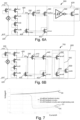
- FIGS 6A and 6B illustrate a voltage limiter 600, 700 according to sixth and seventh example embodiments respectively.
- the voltage limiters 600, 700 differ from the voltage limiter 400 of Figure 4 in that the feedback circuitry further comprises an additional or complementary current sink device 630, in the form of an NMOS transistor, coupled between Vrec 220 and ground 225, in parallel with the main current sink device 410, and a sensing device or sensing gate 640 for sensing current through the main current sink device 410 controlling the additional current sink device 630 and for turning on the additional current sink device 630 when current flows in the main current sink device 410.
- the polarity of the complementary current sink device 630 is opposite to that of the current sink device 410.
- the current through the current sink device 410 depends on the voltage Vlim 435 at the control terminal of the current sink device 410. Accordingly, the input of the sensing gate 640 is connected to the control terminal (gate) of the current sink device 410. The output of the sensing gate 640 is connected to the control terminal of the complementary current sink device 630.
- the sensing gate may be an inverter, a Schmitt trigger, a latch, an amplifier, and/or any other simple, complex or compound gate, sequential or combinational. In the voltage limiter 600 of Figure 6 , the sensing gate 640 is an inverting Schmitt trigger.
- the sensing gate 640 is a MOS inverter comprising a PMOS transistor 642 and an NMOS transistor 644, their control terminals being coupled to the control terminal of the current sink device 410, their sources being coupled to Vrec 220 and ground 225 respectively, their drains both being coupled to the control terminal of the complementary current sink device 630.
- Figure 7 shows a graph illustrating the behaviour of the voltage limiters 600 and 700 of Figures 6A and 6B , compared with that of the voltage limiter 400 of Figure 4 and a typical voltage limiter 100.
- the upper solid line (a) shows the voltage-current characteristics for a typical voltage limiter 100 without the feedback circuitry of the present disclosure.
- the dashed line (b) shows the voltage Vrec 220 output by the RF rectifier of the RFID tag as a function of the current through the current sink device 410, for the voltage limiter 400 of the fourth example embodiment described above with reference to Figure 4 .
- the behaviour of the voltage limiter 400 is the same as that described with respect to curve (b) of Figure 2 .
- the lower solid line (c) shows the voltage Vrec 220 as a function of the current through the current sink device 410, for the voltage limiters 600 and 700 of the sixth and seventh example embodiments described above with reference to Figure 6A and 6B .
- the effect of the complementary current sink device 630 in the voltage limiters 600 and 700 of Figures 6A and 6B is to further flatten the I/V behaviour, causing the reduced voltage (i.e. for currents above around 10E-6 A in Figure 7 ) to remain constant, at a value determined at least in part by the parameters of the complementary current sink device 630, rather than gradually increasing as for the voltage limiter 400 without the complementary sink device 630.
- the complementary current sink device 630 effectively prevents any rise in voltage with increasing current (i.e. increasing proximity to the reader) which could power on the RFID tag.
- FIG 8A illustrates a voltage limiter 800 according to an eighth example embodiment.
- the voltage limiter 800 differs from the voltage limiter 400 of Figure 4 in that the feedback circuitry further comprises a current pull device 835, in the form of an NMOS transistor, coupled between the control terminal of the current sink device 410 and ground 225.
- the polarity of the current pull device 835 is opposite to that of the current sink device 410.
- the voltage limiter 800 also includes a sensing device 640 for sensing the current through the current sink device 410, and for turning on the current pull device 835 when current flows in the main current sink device 410. Accordingly, the input of the sensing gate 640 is connected to the control terminal (gate) of the current sink device 410.
- the output of the sensing gate 640 is connected to the control terminal of the current pull device 835.
- the sensing gate may be an inverter, a Schmitt trigger, a latch, an amplifier, and/or any other simple, complex or compound gate, sequential or combinational.
- the sensing gate 640 is a MOS inverter comprising a PMOS transistor 642 and an NMOS transistor 644, their control terminals being coupled to the control terminal of the current sink device 410, their sources being coupled to Vrec 220 and ground 225 respectively, their drains both being coupled to the control terminal of the current pull device 835.
- FIG 8B illustrates a voltage limiter 900 according to a ninth example embodiment.
- the voltage limiter 900 differs from the voltage limiter 400 of Figure 4 in that the feedback circuitry further comprises a complementary current sink device 630 as disclosed above in connection with Figures 6A and 6B , and a current pull device 835 as disclosed above in connection with Figure 8A .
- the voltage limiter 900 includes a sensing gate 640 for sensing the current through the current sink device 410, the input of the sensing gate 640 being connected to the control terminal (gate) of the current sink device 410.
- the output of the sensing gate 640 is connected to the control terminals of both the complementary current sink device 630 and the current pull device 835.
- Figure 9 shows a graph illustrating the behaviour of the voltage limiter 800 of Figure 8A , compared with that of the voltage limiters 600, 700 of Figures 6A, 6B , the voltage limiter 400 of Figure 4 and a typical voltage limiter 100.
- the upper solid line (a), dashed line (b), and lower solid line (c) are the same as those discussed above with reference to Figure 7 .
- the lowermost solid line (d) shows the voltage Vrec 220 as a function of the current through the current sink device 410, for the voltage limiter 800 of the eighth example embodiment described above with reference to Figure 8A .
- the effect of the current pull device 830 in the voltage limiter 800 of Figure 8A is to clamp the control terminal of the current sink device 410 so that the current sink device 410 is fully turned on, causing the voltage to reduce even more sharply (i.e. at a current of around 4E-6 A).
- the I/V curve (d) in Figure 9 has a sharper edge than curve (b).
- An advantage of this arrangement is that the current pull device 830 may be smaller than the complementary current sink device 630 of Figures 6A and 6B .
- FIG 10 illustrates a voltage limiter 1000 according to a tenth example embodiment.
- the voltage limiter 1000 differs from the voltage limiter 400 of Figure 4 in that the feedback circuitry applies the feedback current to a feedback node 1090 at a different circuitry point.
- a resistor is coupled between the feedback node 1090 and the control terminal of the current sink device 410, thereby generating a voltage offset between the feedback node 1010 and the control terminal of the current sink device 410.
- the resistor 1010 is coupled in series between the transistor m2 and the first diode md1 of the reference generator.
- a similar voltage drop may be achieved using a different passive or active element, for example a diode, bipolar transistor, or MOS transistor, or using a combination of elements.
- Figure 11 shows a graph illustrating the behaviour of the voltage limiter 1010 of the present disclosure, compared with that of the voltage limiter 400 of Figure 4 and a typical voltage limiter 100.
- the upper solid line (a) and dashed line (b) are the same as discussed above with reference to Figure 7 .
- the lower solid line (e) shows the voltage Vrec 220 as a function of the current through the current sink device 410, for the voltage limiter 1000 of the tenth example embodiment described above with reference to Figure 10 .
- the effect of the feedback current passing through a resistor is an upward shift in the value of the reduced voltage level at high currents. Changing the location of the feedback node can therefore be used to adjust the level of the reduced voltage at high currents.
- some applications may require all read and write operations to be disabled at high RF powers, for which the voltage must be reduced below the read threshold, while other applications may require only write operations to be disabled, for which the voltage must be reduced below the write threshold, which is generally higher (e.g. 1V) than the read threshold (e.g. 0.5V).
- the current sink device, current replica device, current mirrors, additional current sink device and current pull device are all based on MOS transistors.
- the current sink device and current replica device have a first polarity.
- the (first) current mirror is based on transistors having a second polarity opposite to the first polarity.
- the skilled person will appreciate that other devices, in particular other types of transistor, could be used.
Landscapes
- Engineering & Computer Science (AREA)
- Computer Hardware Design (AREA)
- Microelectronics & Electronic Packaging (AREA)
- Physics & Mathematics (AREA)
- General Physics & Mathematics (AREA)
- Electromagnetism (AREA)
- Radar, Positioning & Navigation (AREA)
- Automation & Control Theory (AREA)
- Theoretical Computer Science (AREA)
- Tone Control, Compression And Expansion, Limiting Amplitude (AREA)
Abstract
Description
- The present disclosure relates to a voltage limiter for an RFID tag. In particular, but not exclusively, it relates to a voltage limiter incorporated in a radio-frequency identification (RFID) integrated circuit (IC) for an RFID tag, for strongly limiting the voltage at the RFID IC at short distances to an RFID reader.
- State of the art radio-frequency identification (RFID) tags need to deal with a huge input power range. Under high power conditions, when the tag is close to the reader, the integrated circuit (IC) of the RFID tag needs to be protected from physical damage. This is typically achieved by including limiter circuitry to limit the input amplitude to a certain maximum level, defined by the physical limitation of the IC process technology.
- Aspects of the disclosure are set out in the accompanying claims. Combinations of features from the dependent claims may be combined with features of the independent claims as appropriate and not merely as explicitly set out in the claims.
- According to an aspect of the disclosure, there is provided a voltage limiter for a radio-frequency identification (RFID) integrated circuit (IC) for an RFID tag, the RFID IC including a radio-frequency (RF) rectifier, the voltage limiter comprising:
- a current sink device coupled between the output of the RF rectifier and ground;
- a reference generator having an output for providing a reference voltage for controlling a current through the current sink device to limit a voltage at the output of the RF rectifier to values below a predefined voltage level; and
- feedback circuitry arranged to provide a feedback current to the reference generator to vary the reference voltage, the feedback current being dependent on the current through the current sink device.
- By including feedback circuitry arranged to provide a feedback current to the reference generator to vary the reference voltage, the feedback current being dependent on the current through the current sink device, the voltage limiter of the present disclosure can more strongly limit the power to the RFID IC under close-coupled conditions to the reader. This addresses a problem in known limiter circuitry of high-power dissipation through the limiter circuitry under near field (high power) conditions which still impacts the performance and lifetime of the RFID tag IC. By strongly limiting the power under close-coupled conditions to the reader, the voltage limiter of the present disclosure may thereby reduce physical damage to the tag IC. Furthermore, the voltage limiter of the present disclosure enables an anti-spy feature, to prevent intentional reading of the tag in the near field of the reader, thereby increasing privacy in these conditions. This feature guarantees that a tag must be a certain distance from a reader for the tag to be read by that reader, thereby restricting the operating range to a minimum distance.
- In some embodiments, the reference voltage is dependent on the output voltage of the RF rectifier. In other embodiments the reference voltage has a predefined value.
- The feedback current may be proportional to the current through the current sink device, for example a multiple or a submultiple of the current through the current sink device.
- The feedback circuitry may comprise a current replica device coupled between the output of the RF rectifier and ground, in parallel with the current sink device.
- The current replica device may be configured such that a current through the current replica device is dependent on the current through the current sink device. For example, the current through the current replica device may increase with increasing current through the current sink device. In some embodiments, the current through the current replica device is substantially proportional to the current through the current sink device, for example a multiple or submultiple. Providing a current replica branch in addition to the current sink branch, avoids the need to have a diode to mirror the current in the current sink branch, which would limit the sinking capability of the current sink device. For example, if a current mirror were present in the current sink branch, the voltage Vds between the current terminals of the current sink device would be reduced by the voltage Vds between the current terminals of the current mirror. Also, the current replica device provides an additional multiplication (division) ratio between the feedback current and the current in the current sink device, ultimately reducing the area of the voltage limiter.
- A control terminal of the current replica device may be coupled to the control terminal of the current sink device.
- The current replica device may be configured to replicate a multiple or submultiple of the current in the current sink device.
- The feedback circuitry may further comprise at least one current mirror for copying the current in the current replica device.
- By copying or mirroring a current in the current replica branch, the current mirror device does not limit the sinking capability of the current sink device.
- At least one current mirror may comprise a current mirror device coupled in series with the current replica device.
- That is, a current terminal of the current mirror device may be coupled to a current terminal of the current replica device, the other current terminal of the current mirror device being coupled to one of ground or the output of the RF rectifier.
- At least one current mirror may comprise a current mirror device and a current copy device, the current copy device having a control terminal coupled to a control terminal of the current mirror device, a first current terminal coupled to a current terminal of the current mirror device, and a second current terminal coupled to the control terminal of the current sink device.
- A current in said current copy device may be proportional to a current in said current replica device.
- Said at least one current mirror may be configured to mirror a multiple or submultiple of the current in the current replica device.
- Said at least one current mirror may comprise a first current mirror for copying the current in the current replica device, and a further current mirror for copying the current in the first current mirror.
- The inclusion of multiple current mirrors in the feedback circuitry may facilitate different ratios between the feedback current and the current in the current sink device, and/or may facilitate providing the feedback current to different circuitry points of the voltage limiter.
- The feedback circuitry may be configured to provide the feedback current to a control terminal of the current sink device.
- The feedback circuitry may be configured to provide the feedback current to a feedback node of the reference generator, wherein a voltage offset is generated between the feedback node and the control terminal of the current sink device.
- This feature may be used to cause the supply voltage to be reduced to a particular voltage level when the rf power is high. For example, the voltage may be reduced to a level at which read and write to the tag is not possible. As another example, the voltage may be reduced to a level which allows read operations only, but no write operations (as a typical example, read functionality requires a minimum of around 0.5V, while write functionality requires a minimum of around .0V). This feature may also allow the current sink device to be smaller, by causing it to sink less current at high rf powers.
- The feedback circuitry may comprise an element coupled between the feedback node and the control terminal of the current sink device for generating the voltage offset, the element being a resistor, a diode, a bipolar transistor, or a MOS transistor.
- In some embodiments, the current sink device is a main current sink device, the voltage limiter further comprising:
- an additional current sink device coupled between the output of the RF rectifier and the ground, in parallel with the main current sink device; and
- a sensing device for sensing current through the main current sink device and for turning on the additional current sink device when a current flow in the main current sink device exceeds a predetermined level.
- By turning on the additional current sink device when current flows in the main current sink device, the supply voltage is reduced to a fixed voltage level when the rf power is high. This prevents the reduced supply voltage from gradually rising as proximity to an RF reader increases further, since higher RF field amplitudes might otherwise raise the supply voltage sufficiently to actuate the RFID IC. The value of the fixed voltage level may be selected through the choice of device type for the sense device and additional current sink.
- The main sink device and the additional sink device may be transistors having opposite polarity.
- The sensing device may comprise at least one of an inverter, a Schmitt trigger, a latch, and/or an amplifier which may feature a hysteresis.
- The voltage limiter may further comprise:
- a current pull device coupled between the control terminal of the main current sink device and ground; and
- a sensing device for sensing current through the main current sink device and for turning on the current pull device when current flows in the main current sink device.
- By turning on the current pull device when current flows in the main current sink device, the supply voltage is reduced more rapidly as a function of increasing current, due to clamping the control terminal of the current sink device. Another advantage is that this arrangement allows the sensing device and current pull device to be very small.
- The sensing device may comprise at least one of an inverter, a Schmitt trigger, a latch, and/or an amplifier. The sensing device may feature a hysteresis.
- In some embodiments, the current sink device is a main current sink device, the voltage limiter further comprising:
- an additional current sink device coupled between the output of the voltage rectifier and the ground, in parallel with the main current sink device;
- a current pull device coupled between the control terminal of the main current sink device and ground; and
and - a sensing device for sensing current through the main current sink device and for turning on the additional current sink device and the current pull device when current flows in the main current sink device.
- The sensing device may comprise at least one of an inverter, a Schmitt trigger, a latch, and/or an amplifier. The sensing device may feature a hysteresis.
- The current sink device may be a transistor having a first polarity, the transistor comprising a control terminal coupled to the output of the reference generator.
- The current replica device may be a transistor having said first polarity.
- The at least one current mirror may comprise a current mirror having a second polarity opposite to said first polarity.
- According to another aspect of the disclosure, there is provided a radio-frequency identification (RFID) integrated circuit (IC) for an RFID tag, the RFID IC comprising:
- a radio-frequency (RF) rectifier; and
- a voltage limiter according to the preceding aspect of the disclosure.
- According to another aspect of the disclosure, there is provided a method for operating a voltage limiter in a radio-frequency identification (RFID) integrated circuit (IC) for an RFID tag, the RFID IC including a radio-frequency (RF) rectifier, the method comprising:
- sinking a current from the output of the RF rectifier to ground;
- providing a reference voltage for controlling the current to limit a voltage at the output of the RF rectifier to values below a predefined voltage level; and
- providing a feedback current to vary the reference voltage, the feedback current being dependent on the current.
- Example embodiments of the present disclosure will be described, by way of example only, with reference to the accompanying drawings in which like reference signs relate to like elements and in which:
-
Figure 1A schematically illustrates a voltage limiter for an RFID IC useful for understanding the present disclosure; -
Figure 1B schematically illustrates a circuit for a voltage limiter for an RFID IC in accordance with a first example embodiment of the present disclosure; -
Figure 2 shows a graph of input voltage against current sunk illustrating the behaviour of a typical voltage limiter and the voltage limiter according to the first example embodiment of the present disclosure; -
Figure 3A illustrates a circuit for a voltage limiter useful for understanding the present disclosure; -
Figure 3B illustrates a circuit for a voltage limiter in accordance with a second example embodiment of the present disclosure; -
Figure 3C illustrates a circuit for a voltage limiter in accordance with a third example embodiment of the present disclosure; -
Figure 4 illustrates a circuit for a voltage limiter in accordance with a fourth example embodiment of the present disclosure; -
Figure 5 illustrates a circuit for a voltage limiter in accordance with a fifth example embodiment of the present disclosure; -
Figure 6A schematically illustrates a circuit for a voltage limiter in accordance with a sixth example embodiment of the present disclosure; -
Figure 6B illustrates a circuit for a voltage limiter in accordance with a seventh example embodiment of the present disclosure; -
Figure 7 shows a graph of input voltage against current sunk illustrating the behaviour of a typical voltage limiter and the voltage limiter according to the sixth and seventh example embodiments; -
Figure 8A schematically illustrates a circuit for a voltage limiter in accordance with a eighth example embodiment of the present disclosure; -
Figure 8B illustrates a circuit for a voltage limiter in accordance with a ninth example embodiment of the present disclosure; -
Figure 9 shows a graph of input voltage against current sunk illustrating the behaviour of a typical voltage limiter and the voltage limiters according to the eighth and ninth example embodiments; -
Figure 10 illustrates a circuit for a voltage limiter in accordance with a tenth example embodiment of the present disclosure; and -
Figure 11 shows a graph of input voltage against current sunk illustrating the behaviour of a typical voltage limiter and the voltage limiter according to the eleventh example embodiment. -
Figure 1A represents atypical voltage limiter 100, useful for understanding the present invention, thevoltage limiter 100 for a radio-frequency identification (RFID) IC of an RFID tag. The RFID IC includes a radio-frequency (RF) rectifier (not shown) configured to convert an AC signal received from an antenna (not shown) incorporated in the RFID tag to a DC signal. Thevoltage limiter 100 includes acurrent sink device 110 coupled between the output (Vrec) 120 of the RF rectifier and a reference or ground potential (gnd) 125, and areference generator 130 for generating a reference voltage (Vlim) 135 for controlling a current through thecurrent sink device 110 to limit the output voltage of the RF rectifier to a predefined level. -
Figure 1B conceptually illustrates avoltage limiter 200 according to a first example embodiment of the present disclosure. Thevoltage limiter 200 may be incorporated in an RFID IC of an RFID tag. The RFID tag typically includes electronic components to allow the RFID tag to communicate with an external RFID reader, including an RF rectifier (not shown) for generating a DC voltage (Vrec) 230 from an AC signal received from a reader (not shown) through an RFID tag antenna (not shown). Thevoltage limiter 200 includes acurrent sink device 210 coupled between the output (Vrec) 220 of the RF rectifier and a reference or ground potential (gnd) 225. Thevoltage limiter 200 also includes areference generator 230 having anoutput 235 for providing a reference voltage Vlim to the control terminal of thecurrent sink device 210, for controlling a current through thecurrent sink device 210 to limit the output voltage of theRF rectifier Vrec 220 to a predefined voltage level. Thereference voltage Vlim 235 may be derived by thereference generator 230 from thevoltage Vrec 220 output by the RF rectifier. Thecurrent sink device 210 begins to conduct when theoutput voltage 220 of the RF rectifier exceeds a predetermined value. Thereference generator 230 may have a limited driving capability. In contrast to thevoltage limiter 100 ofFigure 1A , thevoltage limiter 200 of this example embodiment also includesfeedback circuitry reference generator 230 to vary thereference voltage Vlim 235 output by thereference generator 230, the feedback current being dependent on the current through thecurrent sink device 210. Thefeedback circuitry current replica device 240, coupled between the output (Vrec) 220 of the RF rectifier and theground potential 225, in parallel with thecurrent sink device 210. The control terminals of thecurrent sink device 210 and thecurrent replica device 240 are connected to each other. A current through the replicacurrent device 240 is proportional to the current through thecurrent sink device 210, for example a multiple or a sub-multiple of it. Thefeedback circuitry current device 240, for example as a multiple or a sub-multiple of it. The copied current is connected (sinking or sourcing) to thereference generator 230 to pull current from the reference voltage Vlim in order to influence the voltage Vlim at theoutput 235 of the reference generator. Thefeedback circuitry current sink device 210 increases. -
Figure 2 shows a graph illustrating the behaviour of thevoltage limiter 200 of the present disclosure and atypical voltage limiter 100. The dashed line (b) ofFigure 2 shows thevoltage Vrec 220 output by the RF rectifier of the RFID tag as a function of the current through thecurrent sink device 210, for thevoltage limiter 200 of the first example embodiment described above with reference toFigure 1B . For comparison, the solid line (a) ofFigure 2 illustrates the corresponding voltage-current characteristics for a typical voltage limiter without the feedback circuitry described in the present disclosure, such as thevoltage limiter 100 shown inFigure 1A . - In
Figure 2 , increasing current corresponds to increasing RF field strength due to increasing proximity to an RF reader. In general, known voltage limiters act to limit the voltage to a pre-determined level as the current increases. Accordingly, the solid line (a) shown inFigure 2 is relatively flat. In contrast, thevoltage limiter 200 of the present disclosure acts to strongly limit the voltage above a specified RF field strength, corresponding to a specified distance to the reader. As can be seen inFigure 2 , the voltage is at a relatively constant level of around 2.3 volts for currents below about 1E-06 amps. As the current increases, corresponding to decreasing distance of the RFID tag from the RF reader, the voltage is sharply pulled down and thereafter remains at a significantly reduced level. In the specific example illustrated inFigure 2 , this sharp decrease occurs between about 4E-6 and 5E-06A, and the voltage is reduced from about 2.3 V to about 0.5 volts. This reduced voltage may gradually increase with further increases to the current, but remains substantially reduced, for example remaining significantly below 1 V. - The effect of the feedback current in the
voltage limiter 200 is thus to automatically reduce the DC voltage supply for the RF tag IC below a predetermined voltage level, for RF field strengths above a predetermined value. The level to which the voltage is reduced is dependent on the size of the devices, in particular the current sink device. As a result, certain functionality of the RFID tag is disabled and can therefore only be used at greater distances from the reader. For example, the supply voltage may be reduced below the level at which the memory cannot be written, or even below the level at which the IC cannot be operated. For example, by limiting the supply voltage to below about 1 volt, both read and write functionality are typically disabled. Some or all operations of the tag may therefore be restricted to be performed only above a minimum distance to the reader. Since this feature is not controlled by a digital signal, but by limiting power to the RFID IC, security may be improved. - Reducing the voltage to the RFID tag IC at high RF powers may also prevent physical damage to the RFID tag IC. This includes reduced self-heating (thermal protection), which in turn reduces the required voltage limiter device size (area improvement) and reduces the parasitic input cap due to the reduced device size (performance improvement). Temperature sensitive applications/products are not disturbed. Power is not burned in the voltage limiter and therefore can be used by other labels in a population (power sharing).
-
Figures 3B and 3C schematically illustrate circuits for avoltage limiter 200 according to second and third respective example embodiments. For comparison,Figure 3A illustrates a circuit for avoltage limiter 100, without the feedback circuitry of the present disclosure, useful for understanding the present disclosure. - Accordingly,
Figure 3A shows avoltage limiter 100 including acurrent sink device 110 in the form of an NMOS transistor coupled between theoutput Vrec 120 of the rectifier of the RFID tag, and aground reference 125. Areference generator 130 comprises avoltage reference 160 for outputting avoltage Vref 165 dependent upon the rectifier output voltage Vrec, and further comprises atransistor 170 and aresistor 180 coupled in series between theoutput Vrec 120 of the rectifier andground 125. The control terminal of thetransistor 170 is controlled by thevoltage Vref 165. Areference voltage Vlim 135 for controlling thecurrent sink device 110 is generated at the connection point between thetransistor 170 andresistor 180, which is coupled to the control terminal ofcurrent sink device 110. -
Figure 3B illustrates avoltage limiter 200 according to a second example embodiment of the present invention. Thevoltage limiter 200 includes acurrent sink device 210, in the form of an NMOS transistor, coupled between the output (Vrec) 220 of the RF rectifier and a reference or ground potential (gnd) 225. Areference generator 230 has anoutput 235 providing areference voltage Vlim 235 which is input to the control terminal (in this embodiment, the gate terminal) of thecurrent sink device 210 for controlling a current through thecurrent sink device 210 to limit the output voltage of the RF rectifier to a predefined voltage level. Thereference generator 230 comprises avoltage reference 260 for outputting avoltage Vref 265 dependent upon the rectifier output voltage Vrec, and further comprises a transistor m, 270, in the form of a PMOS transistor, and a resistor R, 280 coupled in series between theoutput Vrec 220 of the rectifier andground 225. The control terminal (in this embodiment, the gate terminal) of thetransistor 270 is controlled by thevoltage Vref 165 output by the voltage reference. Thereference voltage Vlim 235 for controlling thecurrent sink device 210 is generated at the connection between thetransistor 270 andresistor 280, this connection point being coupled to the control terminal ofcurrent sink device 210. In this embodiment, the reference voltage Vlim increases with theoutput voltage 220 of the RF rectifier. Thecurrent sink device 210 sinks current when thereference voltage Vlim 235 exceeds a predetermined value, in this case the threshold voltage of thecurrent sink device 210. - The
voltage limiter 200 ofFigure 3B embodiment also includesfeedback circuitry reference generator 230 to vary thereference voltage Vlim 235 output by thereference generator 230 for controlling the current through thecurrent sink device 210, the feedback current being dependent on the current through thecurrent sink device 210. - The
feedback circuitry current replica device 240, acurrent mirror device 252 and acurrent copy device 254. Thecurrent replica device 252, in the form of a NMOS transistor, is coupled in parallel with thecurrent sink device 210, between the output (Vrec) 220 of the RF rectifier and the reference orground potential 225. The control terminal of thecurrent replica device 240 is connected to the control terminal of thecurrent sink device 210. A current through thecurrent replica device 240 may be proportional to the current through thecurrent sink device 210, for example a multiple or a sub-multiple of it. Thecurrent mirror device 252 and acurrent copy device 254 together form a current mirror for copying the current in the current replica device 240 (for example a multiple or submultiple of it). Thecurrent mirror device 252, in the form of a PMOS transistor, is coupled in series with thecurrent replica device 240, between theoutput Vrec 220 of the RF rectifier and thecurrent replica device 240. The source terminal of thecurrent mirror device 252 is coupled toVrec 220, while the gate and drain terminals of thecurrent mirror device 252 are connected to each other and are coupled to the drain terminal of thecurrent replica device 240. The copycurrent device 254, in the form of a PMOS transistor, is coupled between theoutput Vrec 220 of the RF rectifier and the control terminal of thecurrent sink device 210. That is, the source terminal of thecurrent copy device 254 is coupled to theVrec 220, the drain terminal of thecurrent copy device 254 is coupled to control terminal of thecurrent sink device 210. The control terminal of the copycurrent device 254 is connected to the control terminal of thecurrent mirror device 252. The current through thecurrent copy device 254 is therefore a copy (e.g. a multiple or submultiple) of the current in thecurrent replica device 240, which is itself a copy (e.g. a multiple or submultiple) of the current in thecurrent sink device 210. The copied current, i.e. the current through thecurrent copy device 252, is fed back to thereference generator 230 at afeedback node 290. In this example embodiment, thefeedback node 290 is connected to the control terminal of thecurrent sink device 210. However, the feedback current may be provided at other circuitry points, as will be illustrated in other example embodiments. The unfilled arrows inFigure 3B indicate the function of thefeedback circuitry current sink device 210 to thecurrent replica device 240, thecurrent mirror device 252, and thecurrent copy device 254 in order to provide, atfeedback node 290, a feedback current which increases with increasing current in thecurrent sink device 210. In this embodiment, the additional feedback current supplied at thefeedback node 290 increases Vlim, causing thecurrent sink device 210 to conduct more strongly, reducing the voltage Vrec. -
Figure 3C illustrates avoltage limiter 300 according to a third example embodiment of the present invention. Thevoltage limiter 300 differs from thevoltage limiter 200 ofFigure 3B in that thefeedback circuitry current mirror current mirror feedback node 292 corresponding to a different circuitry point. Thefeedback node 292 is connected to the output Vref of thevoltage reference 260 and the control terminal of thetransistor 270. The furthercurrent mirror current mirror device 256 and a furthercurrent copy device 258, in the form of NMOS based transistors. The firstcurrent copy device 254 and the furthercurrent mirror device 256 are coupled in series between therectifier output Vrec 220 andground 225, the drain of the firstcurrent copy device 254 being coupled to the drain of the furthercurrent mirror device 256, and the source of the furthercurrent mirror device 256 being coupled toground 225. The furthercurrent copy device 258 is coupled between thefeedback node 292 andground 225. The control terminals (gate terminals) of the further current mirror device and the further current copy device are connected to each other and to the drain of the furthercurrent mirror device 256. Including multiple current mirrors may facilitate different ratios between the feedback current and the current in the current sink device. The feedback current atfeedback node 292 influences the current throughtransistor 270, thereby influencing thevoltage Vlim 235 at the control terminal of thecurrent sink device 210. Compared with the example embodiment ofFigure 3B , the location offeedback node 292 in the example embodiment ofFigure 3C enables the sizes of the devices to be reduced, resulting in an area benefit, and to have a faster response. -
Figure 4 illustrates avoltage limiter 400 according to a fourth example embodiment. Voltage limiters according to the present disclosure may be based on voltage generation architecture comprising a current sink or current source into or from a diode (or multiple diodes). InFigure 4 , a PMOS transistor m1 is coupled in series with a current sink I betweenVrec 220 andground 225. The current through the transistor m1 is mirrored in a second PMOS transistor m2, the source terminal of which is coupled toVrec 220, the drain terminal of which is coupled via multiple series-connected diodes md1, md2, mdN toground 225. Areference voltage Vlim 435 is generated at the connection point between the transistor m2 and the closest diode md1. Thecurrent sink device 410 of this embodiment is provided by a PMOS transistor coupled betweenVrec 220 andground 225. Thereference voltage Vlim 435 is coupled to the control terminal ofcurrent sink device 410. Thecurrent sink device 410 sinks current when the difference between theoutput voltage 220 of the RF rectifier and the reference voltage Vlim exceeds a predetermined value, in this case the threshold voltage of thecurrent sink device 410. Thevoltage limiter 400 ofFigure 4 also includes feedback circuitry comprising acurrent replica device 440, acurrent mirror device 452 and acurrent copy device 454, arranged to provide a feedback current tofeedback node 290 to vary thereference voltage Vlim 435 output by the reference generator for controlling the current through thecurrent sink device 410. Each of thecurrent sink device 410, thecurrent replica device 440, thecurrent mirror device 452 and thecurrent copy device 454 has opposite polarity compared to the corresponding elements of thevoltage limiter 200 ofFigures 3B and 3C . Thecurrent sink device 410 and thecurrent replica device 440 are PMOS transistors, while thecurrent mirror device 452 and thecurrent copy device 454 forming the current mirror are NMOS transistors. - The maximum current at which the
output voltage 220 of the RF rectifier is modified is determined, at least in part, by the driving capability of the reference generator, the current replica ratio and current copy ratio. For example: Iref · nsink · ncopy @vdda ∼ vth_sink (vgs ∼ vds), where Iref is the driving capability of the reference generator, nsink is the ratio between the current through the current replica device and the current through the current sink device, ncopy is the ratio between the copied current and the current through the current replica device, vth_sink is the threshold voltage of the current sink device. Referring toFigure 4 , that is, once the current in thecurrent copy device 454 is more than can be sourced from the transistor m2, vlim drops, resulting in an increased current though thecurrent sink device 410 and a drop in the voltage vrec output by the RF rectifier. -
Figure 5 illustrates avoltage limiter 500 according to a fifth example embodiment. Thevoltage limiter 500 differs from thevoltage limiter 400 ofFigure 4 in that the reference voltage is based on voltage generation architecture which uses a charge pump with limited driving capability. InFigure 5 , thereference voltage Vlim 535 is generated by acharge pump device 580 coupled to aclock generator 585 and referenced to theground potential 225. Thecharge pump device 580 generates thereference voltage Vlim 535 based on aregulated voltage Vreg 590. -
Figures 6A and 6B illustrate avoltage limiter voltage limiters voltage limiter 400 ofFigure 4 in that the feedback circuitry further comprises an additional or complementarycurrent sink device 630, in the form of an NMOS transistor, coupled betweenVrec 220 andground 225, in parallel with the maincurrent sink device 410, and a sensing device orsensing gate 640 for sensing current through the maincurrent sink device 410 controlling the additionalcurrent sink device 630 and for turning on the additionalcurrent sink device 630 when current flows in the maincurrent sink device 410. The polarity of the complementarycurrent sink device 630 is opposite to that of thecurrent sink device 410. The current through thecurrent sink device 410 depends on thevoltage Vlim 435 at the control terminal of thecurrent sink device 410. Accordingly, the input of thesensing gate 640 is connected to the control terminal (gate) of thecurrent sink device 410. The output of thesensing gate 640 is connected to the control terminal of the complementarycurrent sink device 630. The sensing gate may be an inverter, a Schmitt trigger, a latch, an amplifier, and/or any other simple, complex or compound gate, sequential or combinational. In thevoltage limiter 600 ofFigure 6 , thesensing gate 640 is an inverting Schmitt trigger. InFigure 7 , thesensing gate 640 is a MOS inverter comprising aPMOS transistor 642 and anNMOS transistor 644, their control terminals being coupled to the control terminal of thecurrent sink device 410, their sources being coupled toVrec 220 andground 225 respectively, their drains both being coupled to the control terminal of the complementarycurrent sink device 630. -
Figure 7 shows a graph illustrating the behaviour of thevoltage limiters Figures 6A and 6B , compared with that of thevoltage limiter 400 ofFigure 4 and atypical voltage limiter 100. The upper solid line (a) shows the voltage-current characteristics for atypical voltage limiter 100 without the feedback circuitry of the present disclosure. The dashed line (b) shows thevoltage Vrec 220 output by the RF rectifier of the RFID tag as a function of the current through thecurrent sink device 410, for thevoltage limiter 400 of the fourth example embodiment described above with reference toFigure 4 . The behaviour of thevoltage limiter 400 is the same as that described with respect to curve (b) ofFigure 2 . The lower solid line (c) shows thevoltage Vrec 220 as a function of the current through thecurrent sink device 410, for thevoltage limiters Figure 6A and 6B . The effect of the complementarycurrent sink device 630 in thevoltage limiters Figures 6A and 6B is to further flatten the I/V behaviour, causing the reduced voltage (i.e. for currents above around 10E-6 A inFigure 7 ) to remain constant, at a value determined at least in part by the parameters of the complementarycurrent sink device 630, rather than gradually increasing as for thevoltage limiter 400 without thecomplementary sink device 630. The complementarycurrent sink device 630 effectively prevents any rise in voltage with increasing current (i.e. increasing proximity to the reader) which could power on the RFID tag. -
Figure 8A illustrates avoltage limiter 800 according to an eighth example embodiment. Thevoltage limiter 800 differs from thevoltage limiter 400 ofFigure 4 in that the feedback circuitry further comprises acurrent pull device 835, in the form of an NMOS transistor, coupled between the control terminal of thecurrent sink device 410 andground 225. The polarity of thecurrent pull device 835 is opposite to that of thecurrent sink device 410. Thevoltage limiter 800 also includes asensing device 640 for sensing the current through thecurrent sink device 410, and for turning on thecurrent pull device 835 when current flows in the maincurrent sink device 410. Accordingly, the input of thesensing gate 640 is connected to the control terminal (gate) of thecurrent sink device 410. The output of thesensing gate 640 is connected to the control terminal of thecurrent pull device 835. The sensing gate may be an inverter, a Schmitt trigger, a latch, an amplifier, and/or any other simple, complex or compound gate, sequential or combinational. In thevoltage limiter 800 ofFigure 8A , thesensing gate 640 is a MOS inverter comprising aPMOS transistor 642 and anNMOS transistor 644, their control terminals being coupled to the control terminal of thecurrent sink device 410, their sources being coupled toVrec 220 andground 225 respectively, their drains both being coupled to the control terminal of thecurrent pull device 835. -
Figure 8B illustrates avoltage limiter 900 according to a ninth example embodiment. Thevoltage limiter 900 differs from thevoltage limiter 400 ofFigure 4 in that the feedback circuitry further comprises a complementarycurrent sink device 630 as disclosed above in connection withFigures 6A and 6B , and acurrent pull device 835 as disclosed above in connection withFigure 8A . Thevoltage limiter 900 includes asensing gate 640 for sensing the current through thecurrent sink device 410, the input of thesensing gate 640 being connected to the control terminal (gate) of thecurrent sink device 410. The output of thesensing gate 640 is connected to the control terminals of both the complementarycurrent sink device 630 and thecurrent pull device 835. -
Figure 9 shows a graph illustrating the behaviour of thevoltage limiter 800 ofFigure 8A , compared with that of thevoltage limiters Figures 6A, 6B , thevoltage limiter 400 ofFigure 4 and atypical voltage limiter 100. The upper solid line (a), dashed line (b), and lower solid line (c) are the same as those discussed above with reference toFigure 7 . The lowermost solid line (d) shows thevoltage Vrec 220 as a function of the current through thecurrent sink device 410, for thevoltage limiter 800 of the eighth example embodiment described above with reference toFigure 8A . The effect of the current pull device 830 in thevoltage limiter 800 ofFigure 8A is to clamp the control terminal of thecurrent sink device 410 so that thecurrent sink device 410 is fully turned on, causing the voltage to reduce even more sharply (i.e. at a current of around 4E-6 A). Thus the I/V curve (d) inFigure 9 has a sharper edge than curve (b). An advantage of this arrangement is that the current pull device 830 may be smaller than the complementarycurrent sink device 630 ofFigures 6A and 6B . -
Figure 10 illustrates avoltage limiter 1000 according to a tenth example embodiment. Thevoltage limiter 1000 differs from thevoltage limiter 400 ofFigure 4 in that the feedback circuitry applies the feedback current to afeedback node 1090 at a different circuitry point. In thevoltage limiter 1000, a resistor is coupled between thefeedback node 1090 and the control terminal of thecurrent sink device 410, thereby generating a voltage offset between thefeedback node 1010 and the control terminal of thecurrent sink device 410. Theresistor 1010 is coupled in series between the transistor m2 and the first diode md1 of the reference generator. In other embodiments, a similar voltage drop may be achieved using a different passive or active element, for example a diode, bipolar transistor, or MOS transistor, or using a combination of elements. -
Figure 11 shows a graph illustrating the behaviour of thevoltage limiter 1010 of the present disclosure, compared with that of thevoltage limiter 400 ofFigure 4 and atypical voltage limiter 100. The upper solid line (a) and dashed line (b) are the same as discussed above with reference toFigure 7 . The lower solid line (e) shows thevoltage Vrec 220 as a function of the current through thecurrent sink device 410, for thevoltage limiter 1000 of the tenth example embodiment described above with reference toFigure 10 . The effect of the feedback current passing through a resistor is an upward shift in the value of the reduced voltage level at high currents. Changing the location of the feedback node can therefore be used to adjust the level of the reduced voltage at high currents. For example, some applications may require all read and write operations to be disabled at high RF powers, for which the voltage must be reduced below the read threshold, while other applications may require only write operations to be disabled, for which the voltage must be reduced below the write threshold, which is generally higher (e.g. 1V) than the read threshold (e.g. 0.5V). - In the example embodiments described above, the current sink device, current replica device, current mirrors, additional current sink device and current pull device are all based on MOS transistors. The current sink device and current replica device have a first polarity. The (first) current mirror is based on transistors having a second polarity opposite to the first polarity. However, the skilled person will appreciate that other devices, in particular other types of transistor, could be used.
- It will also be appreciated that all the example embodiments disclosed above may be built in their complementary form, that is be replacing NMOS devices by PMOS devices and replacing PMOS devices by NMOS devices.
- Although particular example embodiments of the disclosure have been described above, it will be appreciated than many modifications, including additions and/or substitutions, may be made within the scope of the appended claims.
Claims (15)
- A voltage limiter for a radio-frequency identification, RFID, integrated circuit, IC, for an RFID tag, the RFID IC including a radio-frequency, RF, rectifier, the voltage limiter comprising:a current sink device coupled between the output of the RF rectifier and ground;a reference generator having an output for providing a reference voltage for controlling a current through the current sink device to limit a voltage at the output of the RF rectifier to values below a predefined voltage level; andfeedback circuitry arranged to provide a feedback current to the reference generator to vary the reference voltage, the feedback current being dependent on the current through the current sink device.
- A voltage limited according to claim 1, wherein the feedback circuitry comprises a current replica device coupled between the output of the RF rectifier and ground, in parallel with the current sink device.
- A voltage limiter according to claim 2, wherein a control terminal of the current replica device is coupled to a control terminal of the current sink device.
- A voltage limiter according to claim 2 or claim 3, wherein the current replica device is configured to replicate a multiple or submultiple of the current in the current sink device.
- A voltage limiter according to any one of claims 2 to 4, wherein the feedback circuitry further comprises at least one current mirror for copying the current in the current replica device.
- A voltage limiter according to claim 5, wherein said at least one current mirror is configured to mirror a multiple or submultiple of the current in the current replica device.
- A voltage limiter according to claim 5 or claim 6, wherein said at least one current mirror comprises a first current mirror for copying the current in the current replica device, and a further current mirror for copying the current in the first current mirror.
- A voltage limiter according to any one of the preceding claims, wherein the feedback circuitry is configured to provide the feedback current to a control terminal of the current sink device.
- A voltage limiter according to any one of claims 1 to 7, wherein the feedback circuitry is configured to provide the feedback current to a feedback node of the reference generator, wherein a voltage offset is generated between the feedback node and the control terminal of the current sink device.
- A voltage limiter according to claim 9, wherein the feedback circuitry comprises an element coupled between the feedback node and the control terminal of the current sink device for generating the voltage offset, the element being a resistor, a diode, a bipolar transistor, or a MOS transistor.
- A voltage limiter according to any one of the preceding claims, wherein the current sink device is a main current sink device, the voltage limiter further comprising:an additional current sink device coupled between the output of the RF rectifier and the ground, in parallel with the main current sink device; anda sensing device for sensing current through the main current sink device and for turning on the additional current sink device when a current in the main current sink device exceeds a predetermined level.
- A voltage limiter according to any one of the preceding claims, further comprising:a current pull device coupled between the control terminal of the main current sink device and ground; anda sensing device for sensing current through the main current sink device and for turning on the current pull device when current flows in the main current sink device.
- A voltage limiter according to claim 11 or claim 12, wherein the sensing device comprises at least one of an inverter, a Schmitt trigger, a latch, and/or an amplifier.
- A voltage limiter according to any one of the preceding claims, comprising at least one of the following features:wherein the current sink device is a transistor having a first polarity, the transistor comprising a control terminal coupled to the output of the reference generator;wherein the current replica device is a transistor having said first polarity; andthe at least one current mirror comprises a current mirror device having a second polarity opposite to said first polarity.
- A radio-frequency identification, RFID, integrated circuit, IC, for an RFID tag, the RFID IC comprising:a radio-frequency rectifier; anda voltage limiter according to any one of the preceding claims.
Priority Applications (3)
| Application Number | Priority Date | Filing Date | Title |
|---|---|---|---|
| EP22171932.1A EP4273749B1 (en) | 2022-05-05 | 2022-05-05 | Voltage limiter for an rfid tag |
| US18/298,005 US12372992B2 (en) | 2022-05-05 | 2023-04-10 | Voltage limiter for an RFID tag |
| CN202310489941.5A CN117013512A (en) | 2022-05-05 | 2023-05-04 | Voltage limiter for RFID tag |
Applications Claiming Priority (1)
| Application Number | Priority Date | Filing Date | Title |
|---|---|---|---|
| EP22171932.1A EP4273749B1 (en) | 2022-05-05 | 2022-05-05 | Voltage limiter for an rfid tag |
Publications (2)
| Publication Number | Publication Date |
|---|---|
| EP4273749A1 true EP4273749A1 (en) | 2023-11-08 |
| EP4273749B1 EP4273749B1 (en) | 2025-01-08 |
Family
ID=81585181
Family Applications (1)
| Application Number | Title | Priority Date | Filing Date |
|---|---|---|---|
| EP22171932.1A Active EP4273749B1 (en) | 2022-05-05 | 2022-05-05 | Voltage limiter for an rfid tag |
Country Status (3)
| Country | Link |
|---|---|
| US (1) | US12372992B2 (en) |
| EP (1) | EP4273749B1 (en) |
| CN (1) | CN117013512A (en) |
Citations (2)
| Publication number | Priority date | Publication date | Assignee | Title |
|---|---|---|---|---|
| US20160314389A1 (en) * | 2014-01-08 | 2016-10-27 | Excelio Technology (Shenzhen) Co.,Ltd. | Limiter circuit capable of continuously adjusting amplitude of rectified signal and passive radio frequency tag |
| EP3113082A2 (en) * | 2015-06-29 | 2017-01-04 | EM Microelectronic-Marin SA | Rfid transponder with rectifier and voltage limiter |
Family Cites Families (25)
| Publication number | Priority date | Publication date | Assignee | Title |
|---|---|---|---|---|
| US4127885A (en) | 1977-04-21 | 1978-11-28 | Rca Corporation | Over-current protection circuit for voltage regulator |
| GB9027111D0 (en) | 1990-12-13 | 1991-02-06 | Raychem Ltd | Circuit protection device |
| EP0614136B1 (en) | 1993-03-04 | 1999-07-07 | Alcatel | Power supply shunt regulator |
| US6141193A (en) | 1999-03-15 | 2000-10-31 | National Semiconductor Corporation | Shunt regulator with shutdown protection to prevent excessive power dissipation |
| CN1193283C (en) | 2001-01-02 | 2005-03-16 | 深圳赛意法微电子有限公司 | Current-limiting protection circuit for voltage stabilizer |
| FR2830091B1 (en) | 2001-09-25 | 2004-09-10 | St Microelectronics Sa | VOLTAGE REGULATOR INCORPORATING A STABILIZATION RESISTOR AND A CIRCUIT FOR LIMITING THE OUTPUT CURRENT |
| JP2003216252A (en) | 2001-11-15 | 2003-07-31 | Seiko Instruments Inc | Voltage regulator |
| US6861832B2 (en) * | 2003-06-02 | 2005-03-01 | Texas Instruments Incorporated | Threshold voltage adjustment for MOS devices |
| US7494066B2 (en) * | 2003-12-19 | 2009-02-24 | Semiconductor Energy Laboratory Co., Ltd. | Semiconductor device |
| US20070206338A1 (en) | 2004-08-10 | 2007-09-06 | Tsutomu Ishino | Circuit Protection Method, Protection Circuit and Power Supply Device Using The Protection Circuit |
| US7602161B2 (en) | 2006-05-05 | 2009-10-13 | Standard Microsystems Corporation | Voltage regulator with inherent voltage clamping |
| US7808387B1 (en) * | 2007-06-07 | 2010-10-05 | Impinj, Inc. | Voltage reference circuit with low-power bandgap |
| ITTO20070563A1 (en) * | 2007-07-30 | 2009-01-31 | St Microelectronics Srl | RADIOFREQUENCY IDENTIFICATION DEVICE WITH COUPLED ANTENNA IN NEAR FIELD |
| US7423416B1 (en) | 2007-09-12 | 2008-09-09 | Freescale Semiconductor, Inc. | Voltage regulator and method for providing a regulated output |
| GB0722516D0 (en) | 2007-11-15 | 2007-12-27 | Innovision Res & Tech Plc | Near field communication devices |
| TW201017359A (en) | 2008-10-20 | 2010-05-01 | Advanced Analog Technology Inc | Low dropout regulator having a current-limiting mechanism |
| US8841890B2 (en) * | 2011-06-10 | 2014-09-23 | Cypress Semiconductor Corporation | Shunt regulator circuit having a split output |
| JP5895369B2 (en) | 2011-06-14 | 2016-03-30 | ミツミ電機株式会社 | Semiconductor integrated circuit for regulator |
| KR102013402B1 (en) * | 2012-08-13 | 2019-08-22 | 삼성전자주식회사 | Radio frequency identification device |
| CN103699929B (en) * | 2014-01-08 | 2017-01-04 | 卓捷创芯科技(深圳)有限公司 | The rectification that a kind of switching signal controls and amplitude limiter circuit and passive RF label |
| FR3023434B1 (en) * | 2014-07-02 | 2017-10-13 | Stmicroelectronics Rousset | VOLTAGE AND POWER LIMITER FOR ELECTROMAGNETIC TRANSPONDER |
| US20160187900A1 (en) | 2014-12-24 | 2016-06-30 | Kailash Dhiman | Voltage regulator circuit and method for limiting inrush current |
| US10572789B1 (en) * | 2015-06-26 | 2020-02-25 | Impinj, Inc. | Impedance-change mitigation in RFID tags |
| JP7096673B2 (en) | 2018-01-29 | 2022-07-06 | ローム株式会社 | regulator |
| US11720778B2 (en) | 2021-08-24 | 2023-08-08 | Nxp B.V. | Voltage limiter |
-
2022
- 2022-05-05 EP EP22171932.1A patent/EP4273749B1/en active Active
-
2023
- 2023-04-10 US US18/298,005 patent/US12372992B2/en active Active
- 2023-05-04 CN CN202310489941.5A patent/CN117013512A/en active Pending
Patent Citations (2)
| Publication number | Priority date | Publication date | Assignee | Title |
|---|---|---|---|---|
| US20160314389A1 (en) * | 2014-01-08 | 2016-10-27 | Excelio Technology (Shenzhen) Co.,Ltd. | Limiter circuit capable of continuously adjusting amplitude of rectified signal and passive radio frequency tag |
| EP3113082A2 (en) * | 2015-06-29 | 2017-01-04 | EM Microelectronic-Marin SA | Rfid transponder with rectifier and voltage limiter |
Also Published As
| Publication number | Publication date |
|---|---|
| US12372992B2 (en) | 2025-07-29 |
| CN117013512A (en) | 2023-11-07 |
| US20230359234A1 (en) | 2023-11-09 |
| EP4273749B1 (en) | 2025-01-08 |
Similar Documents
| Publication | Publication Date | Title |
|---|---|---|
| US10454466B1 (en) | Biasing cascode transistors of an output buffer circuit for operation over a wide range of supply voltages | |
| US10168363B1 (en) | Current sensor with extended voltage range | |
| JP4937865B2 (en) | Constant voltage circuit | |
| US20160357206A1 (en) | Ldo regulator with improved load transient performance for internal power supply | |
| US9882558B1 (en) | Power-on reset circuit | |
| JP5279544B2 (en) | Voltage regulator | |
| KR100335496B1 (en) | Internal voltage generation circuit that can operate safely under low power voltage VCC | |
| KR100939293B1 (en) | Shunt Regulators and Electronic Devices | |
| CN110045777B (en) | Reverse current prevention circuit and power supply circuit | |
| US7349190B1 (en) | Resistor-less accurate low voltage detect circuit and method for detecting a low voltage condition | |
| JP4981267B2 (en) | Overheat detection circuit | |
| EP4286977A1 (en) | Fast-transient buffer | |
| EP2239645A1 (en) | Band gap reference circuit and method for operating a band gap reference circuit | |
| US8143878B2 (en) | Starter circuit, bandgap circuit and monitoring circuit | |
| US12416933B2 (en) | Low voltage drop output regulator for preventing inrush current and method for controlling thereof | |
| US9772647B2 (en) | Powering of a charge with a floating node | |
| US12372992B2 (en) | Voltage limiter for an RFID tag | |
| JP4727294B2 (en) | Power circuit | |
| CN111585552A (en) | Output driver circuit | |
| EP3435193B1 (en) | Current and voltage regulation method to improve electromagnetic compatibility performance | |
| JP2011188361A (en) | Power-on reset circuit | |
| KR100633598B1 (en) | Half Supply Voltage Generation Circuit | |
| KR970003188B1 (en) | Ac voltage clipper in mos-technology | |
| US7626845B2 (en) | Voltage programming switch for one-time-programmable (OTP) memories | |
| US20240039494A1 (en) | Operational Amplifier |
Legal Events
| Date | Code | Title | Description |
|---|---|---|---|
| PUAI | Public reference made under article 153(3) epc to a published international application that has entered the european phase |
Free format text: ORIGINAL CODE: 0009012 |
|
| STAA | Information on the status of an ep patent application or granted ep patent |
Free format text: STATUS: THE APPLICATION HAS BEEN PUBLISHED |
|
| AK | Designated contracting states |
Kind code of ref document: A1 Designated state(s): AL AT BE BG CH CY CZ DE DK EE ES FI FR GB GR HR HU IE IS IT LI LT LU LV MC MK MT NL NO PL PT RO RS SE SI SK SM TR |
|
| STAA | Information on the status of an ep patent application or granted ep patent |
Free format text: STATUS: REQUEST FOR EXAMINATION WAS MADE |
|
| 17P | Request for examination filed |
Effective date: 20240508 |
|
| RBV | Designated contracting states (corrected) |
Designated state(s): AL AT BE BG CH CY CZ DE DK EE ES FI FR GB GR HR HU IE IS IT LI LT LU LV MC MK MT NL NO PL PT RO RS SE SI SK SM TR |
|
| GRAP | Despatch of communication of intention to grant a patent |
Free format text: ORIGINAL CODE: EPIDOSNIGR1 |
|
| STAA | Information on the status of an ep patent application or granted ep patent |
Free format text: STATUS: GRANT OF PATENT IS INTENDED |
|
| INTG | Intention to grant announced |
Effective date: 20240904 |
|
| GRAS | Grant fee paid |
Free format text: ORIGINAL CODE: EPIDOSNIGR3 |
|
| GRAA | (expected) grant |
Free format text: ORIGINAL CODE: 0009210 |
|
| STAA | Information on the status of an ep patent application or granted ep patent |
Free format text: STATUS: THE PATENT HAS BEEN GRANTED |
|
| AK | Designated contracting states |
Kind code of ref document: B1 Designated state(s): AL AT BE BG CH CY CZ DE DK EE ES FI FR GB GR HR HU IE IS IT LI LT LU LV MC MK MT NL NO PL PT RO RS SE SI SK SM TR |
|
| REG | Reference to a national code |
Ref country code: GB Ref legal event code: FG4D |
|
| REG | Reference to a national code |
Ref country code: CH Ref legal event code: EP |
|
| REG | Reference to a national code |
Ref country code: DE Ref legal event code: R096 Ref document number: 602022009492 Country of ref document: DE |
|
| REG | Reference to a national code |
Ref country code: IE Ref legal event code: FG4D |
|
| REG | Reference to a national code |
Ref country code: LT Ref legal event code: MG9D |
|
| REG | Reference to a national code |
Ref country code: NL Ref legal event code: MP Effective date: 20250108 |
|
| REG | Reference to a national code |
Ref country code: AT Ref legal event code: MK05 Ref document number: 1758818 Country of ref document: AT Kind code of ref document: T Effective date: 20250108 |
|
| PG25 | Lapsed in a contracting state [announced via postgrant information from national office to epo] |
Ref country code: NL Free format text: LAPSE BECAUSE OF FAILURE TO SUBMIT A TRANSLATION OF THE DESCRIPTION OR TO PAY THE FEE WITHIN THE PRESCRIBED TIME-LIMIT Effective date: 20250108 |
|
| PG25 | Lapsed in a contracting state [announced via postgrant information from national office to epo] |
Ref country code: RS Free format text: LAPSE BECAUSE OF FAILURE TO SUBMIT A TRANSLATION OF THE DESCRIPTION OR TO PAY THE FEE WITHIN THE PRESCRIBED TIME-LIMIT Effective date: 20250408 |
|
| PG25 | Lapsed in a contracting state [announced via postgrant information from national office to epo] |
Ref country code: PL Free format text: LAPSE BECAUSE OF FAILURE TO SUBMIT A TRANSLATION OF THE DESCRIPTION OR TO PAY THE FEE WITHIN THE PRESCRIBED TIME-LIMIT Effective date: 20250108 |
|
| PGFP | Annual fee paid to national office [announced via postgrant information from national office to epo] |
Ref country code: DE Payment date: 20250423 Year of fee payment: 4 |
|
| PG25 | Lapsed in a contracting state [announced via postgrant information from national office to epo] |
Ref country code: ES Free format text: LAPSE BECAUSE OF FAILURE TO SUBMIT A TRANSLATION OF THE DESCRIPTION OR TO PAY THE FEE WITHIN THE PRESCRIBED TIME-LIMIT Effective date: 20250108 |
|
| PG25 | Lapsed in a contracting state [announced via postgrant information from national office to epo] |
Ref country code: NO Free format text: LAPSE BECAUSE OF FAILURE TO SUBMIT A TRANSLATION OF THE DESCRIPTION OR TO PAY THE FEE WITHIN THE PRESCRIBED TIME-LIMIT Effective date: 20250408 Ref country code: IS Free format text: LAPSE BECAUSE OF FAILURE TO SUBMIT A TRANSLATION OF THE DESCRIPTION OR TO PAY THE FEE WITHIN THE PRESCRIBED TIME-LIMIT Effective date: 20250508 |
|
| PG25 | Lapsed in a contracting state [announced via postgrant information from national office to epo] |
Ref country code: HR Free format text: LAPSE BECAUSE OF FAILURE TO SUBMIT A TRANSLATION OF THE DESCRIPTION OR TO PAY THE FEE WITHIN THE PRESCRIBED TIME-LIMIT Effective date: 20250108 |
|
| PG25 | Lapsed in a contracting state [announced via postgrant information from national office to epo] |
Ref country code: PT Free format text: LAPSE BECAUSE OF FAILURE TO SUBMIT A TRANSLATION OF THE DESCRIPTION OR TO PAY THE FEE WITHIN THE PRESCRIBED TIME-LIMIT Effective date: 20250508 Ref country code: LV Free format text: LAPSE BECAUSE OF FAILURE TO SUBMIT A TRANSLATION OF THE DESCRIPTION OR TO PAY THE FEE WITHIN THE PRESCRIBED TIME-LIMIT Effective date: 20250108 |
|
| PGFP | Annual fee paid to national office [announced via postgrant information from national office to epo] |
Ref country code: FR Payment date: 20250423 Year of fee payment: 4 |
|
| PG25 | Lapsed in a contracting state [announced via postgrant information from national office to epo] |
Ref country code: BG Free format text: LAPSE BECAUSE OF FAILURE TO SUBMIT A TRANSLATION OF THE DESCRIPTION OR TO PAY THE FEE WITHIN THE PRESCRIBED TIME-LIMIT Effective date: 20250108 Ref country code: GR Free format text: LAPSE BECAUSE OF FAILURE TO SUBMIT A TRANSLATION OF THE DESCRIPTION OR TO PAY THE FEE WITHIN THE PRESCRIBED TIME-LIMIT Effective date: 20250409 |
|
| PG25 | Lapsed in a contracting state [announced via postgrant information from national office to epo] |
Ref country code: AT Free format text: LAPSE BECAUSE OF FAILURE TO SUBMIT A TRANSLATION OF THE DESCRIPTION OR TO PAY THE FEE WITHIN THE PRESCRIBED TIME-LIMIT Effective date: 20250108 |
|
| PG25 | Lapsed in a contracting state [announced via postgrant information from national office to epo] |
Ref country code: SE Free format text: LAPSE BECAUSE OF FAILURE TO SUBMIT A TRANSLATION OF THE DESCRIPTION OR TO PAY THE FEE WITHIN THE PRESCRIBED TIME-LIMIT Effective date: 20250108 |
|
| PG25 | Lapsed in a contracting state [announced via postgrant information from national office to epo] |
Ref country code: SM Free format text: LAPSE BECAUSE OF FAILURE TO SUBMIT A TRANSLATION OF THE DESCRIPTION OR TO PAY THE FEE WITHIN THE PRESCRIBED TIME-LIMIT Effective date: 20250108 |
|
| REG | Reference to a national code |
Ref country code: DE Ref legal event code: R097 Ref document number: 602022009492 Country of ref document: DE |
|
| PG25 | Lapsed in a contracting state [announced via postgrant information from national office to epo] |
Ref country code: DK Free format text: LAPSE BECAUSE OF FAILURE TO SUBMIT A TRANSLATION OF THE DESCRIPTION OR TO PAY THE FEE WITHIN THE PRESCRIBED TIME-LIMIT Effective date: 20250108 |
|
| PG25 | Lapsed in a contracting state [announced via postgrant information from national office to epo] |
Ref country code: EE Free format text: LAPSE BECAUSE OF FAILURE TO SUBMIT A TRANSLATION OF THE DESCRIPTION OR TO PAY THE FEE WITHIN THE PRESCRIBED TIME-LIMIT Effective date: 20250108 Ref country code: CZ Free format text: LAPSE BECAUSE OF FAILURE TO SUBMIT A TRANSLATION OF THE DESCRIPTION OR TO PAY THE FEE WITHIN THE PRESCRIBED TIME-LIMIT Effective date: 20250108 |
|
| PG25 | Lapsed in a contracting state [announced via postgrant information from national office to epo] |
Ref country code: RO Free format text: LAPSE BECAUSE OF FAILURE TO SUBMIT A TRANSLATION OF THE DESCRIPTION OR TO PAY THE FEE WITHIN THE PRESCRIBED TIME-LIMIT Effective date: 20250108 |
|
| PG25 | Lapsed in a contracting state [announced via postgrant information from national office to epo] |
Ref country code: SK Free format text: LAPSE BECAUSE OF FAILURE TO SUBMIT A TRANSLATION OF THE DESCRIPTION OR TO PAY THE FEE WITHIN THE PRESCRIBED TIME-LIMIT Effective date: 20250108 |
|
| PLBE | No opposition filed within time limit |
Free format text: ORIGINAL CODE: 0009261 |
|
| STAA | Information on the status of an ep patent application or granted ep patent |
Free format text: STATUS: NO OPPOSITION FILED WITHIN TIME LIMIT |
|
| REG | Reference to a national code |
Ref country code: CH Ref legal event code: L10 Free format text: ST27 STATUS EVENT CODE: U-0-0-L10-L00 (AS PROVIDED BY THE NATIONAL OFFICE) Effective date: 20251119 |
|
| 26N | No opposition filed |
Effective date: 20251009 |
|
| REG | Reference to a national code |
Ref country code: CH Ref legal event code: H13 Free format text: ST27 STATUS EVENT CODE: U-0-0-H10-H13 (AS PROVIDED BY THE NATIONAL OFFICE) Effective date: 20251223 |
|
| PG25 | Lapsed in a contracting state [announced via postgrant information from national office to epo] |
Ref country code: LU Free format text: LAPSE BECAUSE OF NON-PAYMENT OF DUE FEES Effective date: 20250505 |
|
| PG25 | Lapsed in a contracting state [announced via postgrant information from national office to epo] |
Ref country code: CH Free format text: LAPSE BECAUSE OF NON-PAYMENT OF DUE FEES Effective date: 20250531 |
|
| PG25 | Lapsed in a contracting state [announced via postgrant information from national office to epo] |
Ref country code: IT Free format text: LAPSE BECAUSE OF FAILURE TO SUBMIT A TRANSLATION OF THE DESCRIPTION OR TO PAY THE FEE WITHIN THE PRESCRIBED TIME-LIMIT Effective date: 20250108 |
|
| REG | Reference to a national code |
Ref country code: BE Ref legal event code: MM Effective date: 20250531 |
|
| PG25 | Lapsed in a contracting state [announced via postgrant information from national office to epo] |
Ref country code: MC Free format text: LAPSE BECAUSE OF FAILURE TO SUBMIT A TRANSLATION OF THE DESCRIPTION OR TO PAY THE FEE WITHIN THE PRESCRIBED TIME-LIMIT Effective date: 20250108 |
|
| PG25 | Lapsed in a contracting state [announced via postgrant information from national office to epo] |
Ref country code: IE Free format text: LAPSE BECAUSE OF NON-PAYMENT OF DUE FEES Effective date: 20250505 |
|
| PG25 | Lapsed in a contracting state [announced via postgrant information from national office to epo] |
Ref country code: BE Free format text: LAPSE BECAUSE OF NON-PAYMENT OF DUE FEES Effective date: 20250531 |