EP4273702A1 - Operating method of memory device for managing map data of each of plurality of storage devices, computing system including memory device, and operating method of computing system - Google Patents
Operating method of memory device for managing map data of each of plurality of storage devices, computing system including memory device, and operating method of computing system Download PDFInfo
- Publication number
- EP4273702A1 EP4273702A1 EP23171249.8A EP23171249A EP4273702A1 EP 4273702 A1 EP4273702 A1 EP 4273702A1 EP 23171249 A EP23171249 A EP 23171249A EP 4273702 A1 EP4273702 A1 EP 4273702A1
- Authority
- EP
- European Patent Office
- Prior art keywords
- cxl
- memory
- storage
- storage device
- map data
- Prior art date
- Legal status (The legal status is an assumption and is not a legal conclusion. Google has not performed a legal analysis and makes no representation as to the accuracy of the status listed.)
- Pending
Links
- 238000003860 storage Methods 0.000 title claims abstract description 502
- 238000011017 operating method Methods 0.000 title claims abstract description 25
- 230000015654 memory Effects 0.000 claims description 477
- 230000004044 response Effects 0.000 claims description 112
- 238000013507 mapping Methods 0.000 claims description 13
- 238000004891 communication Methods 0.000 claims description 5
- 238000000034 method Methods 0.000 abstract description 2
- 101150101057 PBA1 gene Proteins 0.000 description 25
- 101000648827 Homo sapiens TPR and ankyrin repeat-containing protein 1 Proteins 0.000 description 23
- 102100028173 TPR and ankyrin repeat-containing protein 1 Human genes 0.000 description 23
- 238000012546 transfer Methods 0.000 description 23
- 238000010586 diagram Methods 0.000 description 14
- 230000000630 rising effect Effects 0.000 description 8
- 230000014759 maintenance of location Effects 0.000 description 7
- 238000007726 management method Methods 0.000 description 4
- 238000012545 processing Methods 0.000 description 4
- 239000004744 fabric Substances 0.000 description 3
- 230000008859 change Effects 0.000 description 2
- 238000012937 correction Methods 0.000 description 2
- 230000009977 dual effect Effects 0.000 description 2
- 230000003287 optical effect Effects 0.000 description 2
- 238000013519 translation Methods 0.000 description 2
- 230000003936 working memory Effects 0.000 description 2
- 230000005540 biological transmission Effects 0.000 description 1
- CXOXHMZGEKVPMT-UHFFFAOYSA-N clobazam Chemical compound O=C1CC(=O)N(C)C2=CC=C(Cl)C=C2N1C1=CC=CC=C1 CXOXHMZGEKVPMT-UHFFFAOYSA-N 0.000 description 1
- 238000013461 design Methods 0.000 description 1
- 238000001514 detection method Methods 0.000 description 1
- 238000005516 engineering process Methods 0.000 description 1
- 239000000835 fiber Substances 0.000 description 1
- 230000006870 function Effects 0.000 description 1
- 230000036541 health Effects 0.000 description 1
- 230000010354 integration Effects 0.000 description 1
- 238000012986 modification Methods 0.000 description 1
- 230000004048 modification Effects 0.000 description 1
- 230000001537 neural effect Effects 0.000 description 1
- 229940044442 onfi Drugs 0.000 description 1
- 230000008569 process Effects 0.000 description 1
- 239000007787 solid Substances 0.000 description 1
- 230000003068 static effect Effects 0.000 description 1
- 230000001360 synchronised effect Effects 0.000 description 1
Images


Classifications
-
- G—PHYSICS
- G06—COMPUTING; CALCULATING OR COUNTING
- G06F—ELECTRIC DIGITAL DATA PROCESSING
- G06F12/00—Accessing, addressing or allocating within memory systems or architectures
- G06F12/02—Addressing or allocation; Relocation
- G06F12/0223—User address space allocation, e.g. contiguous or non contiguous base addressing
- G06F12/023—Free address space management
- G06F12/0238—Memory management in non-volatile memory, e.g. resistive RAM or ferroelectric memory
- G06F12/0246—Memory management in non-volatile memory, e.g. resistive RAM or ferroelectric memory in block erasable memory, e.g. flash memory
-
- G—PHYSICS
- G06—COMPUTING; CALCULATING OR COUNTING
- G06F—ELECTRIC DIGITAL DATA PROCESSING
- G06F2212/00—Indexing scheme relating to accessing, addressing or allocation within memory systems or architectures
- G06F2212/72—Details relating to flash memory management
- G06F2212/7201—Logical to physical mapping or translation of blocks or pages
Definitions
- Embodiments of the present disclosure described herein relate to a memory device, and more particularly, relate to a memory device managing map data of each of a plurality of storage devices.
- a memory device stores data in response to a write request and outputs data stored therein in response to a read request.
- the memory device is classified as a volatile memory device, which loses data stored therein when a power supply is interrupted, such as a dynamic random access memory (DRAM) device, a static RAM (SRAM) device, or a nonvolatile memory device, which retains data stored therein even when a power supply is interrupted, such as a flash memory device, a phase-change RAM (PRAM), a magnetic RAM (MRAM), or a resistive RAM (RRAM).
- DRAM dynamic random access memory
- SRAM static RAM
- RRAM resistive RAM
- the nonvolatile memory device may be used as a storage device storing a large amount of data.
- the number of storage devices capable of being connected with a host may be limited depending on an interface of the host.
- SSD solid state drive
- an SSD device including a plurality of storage devices may be required regardless of the limitation on the number of storage devices capable of being connected with the host.
- Embodiments of the present disclosure provide an operating method of a memory device managing map data of each of a plurality of storage devices, a computing system including the memory device, and an operating method of the computing system.
- an operating method of a memory device which communicates with a first storage device and a second storage device through an interface circuit, the operating method including: receiving, from a host device, a first request including a command and a first logical block address; obtaining, based on the first logical block address, a first physical block address with reference to first map data dedicated for the first storage device; and sending, to the first storage device through the interface circuit, a second request including the first physical block address and the command.
- a computing system including: a first storage device; a second storage device; a memory device storing a mapping table for managing first map data dedicated for the first storage device and second map data dedicated for the second storage device; and an interface circuit configured to communicate with the first storage device, the second storage device, and the memory device, wherein the memory device is configured to: receive, from a host device, a first request including a command and a first logical block address, obtain, based on the first logical block address, a first physical block address with reference to the first map data of the mapping table, and send, to the first storage device through the interface circuit, a second request including the first physical block address and the command.
- an operating method of a computing system which includes a first storage device, a second storage device, a memory device, and an interface circuit communicating with the first storage device, the second storage device, and the memory device, the operating method including: receiving, by the memory device, a first request including a command and a first logical block address from a host device; obtaining, by the memory device, a first physical block address with reference to first map data dedicated for the first storage device, based on the first logical block address; and sending, by the memory device, a second request including the first physical block address and the command to the first storage device through the interface circuit.
- FIG. 1 is a block diagram illustrating a computing system including a storage device.
- a computing system 10 may include a host 11, a plurality of memory devices 12a and 12b, and a storage device 13.
- the host 11 may control an overall operation of the computing system 10.
- the plurality of memory devices 12a and 12b may be used as a working memory or a system memory of the host 11.
- the storage device 13 may include a storage controller 13a, a buffer memory 13b, and a nonvolatile memory 13c. Under control of the host 11, the storage controller 13a may store data in the nonvolatile memory 13c or may send data stored in the nonvolatile memory 13c to the host 11.
- the buffer memory 13b may store a variety of information necessary for the storage device 13 to operate.
- the storage controller 13a may manage data stored in the nonvolatile memory 13c by using map data.
- the map data may include information about relationship between a logical block address managed by the host 11 and a physical block address of the nonvolatile memory 13c.
- the buffer memory 13b may be a high-speed memory such as a DRAM.
- the capacity of the nonvolatile memory 13c increases, the size of necessary map data may increase.
- the capacity of the buffer memory 13b included in the single storage device 13 is limited, it is impossible to cope with the increase in the size of the map data due to the increase in the capacity of the nonvolatile memory 13c.
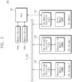
- FIG. 2 is a block diagram illustrating a computing system to which a storage system according to an embodiment of the present disclosure is applied.
- a computing system 100 may include a host 101, a plurality of memory devices 102a and 102b, first Compute Express Link (CXL) storage 120, second CXL storage 130, and a CXL memory 110.
- the computing system 100 may be included in user devices such as a personal computer, a laptop computer, a server, a media player, and a digital camera or automotive devices such as a navigation system, a black box, and an automotive electronic device/part.
- the computing system 100 may be a mobile system such as a mobile phone, a smartphone, a tablet personal computer (PC), a wearable device, a health care device, or an Internet of things (IoT) device.
- IoT Internet of things
- the host 101 may control an overall operation of the computing system 100.
- the host 101 may be one of various processors such as a central processing unit (CPU), a graphics processing unit (GPU), a neural processing unit (NPU), and a data processing unit (DPU).
- the host 101 may include a single core processor or a multi-core processor.
- the plurality of memory devices 102a and 102b may be used as a main memory or a system memory of the computing system 100.
- each of the plurality of memory devices 102a and 102b may be a dynamic random access memory (DRAM) device and may have the form factor of the dual in-line memory module (DIMM).
- DIMM dual in-line memory module
- the present disclosure is not limited thereto.
- the plurality of memory devices 102a and 102b may include a nonvolatile memory such as a flash memory, a phase change RAM (PRAM), a resistive RAM (RRAM), or a magnetic RAM (MRAM).
- PRAM phase change RAM
- RRAM resistive RAM
- MRAM magnetic RAM
- the plurality of memory devices 102a and 102b may directly communicate with the host 101 through the DDR interface.
- the host 101 may include a memory controller configured to control the plurality of memory devices 102a and 102b.
- the present disclosure is not limited thereto.
- the plurality of memory devices 102a and 102b may communicate with the host 101 through various interfaces.
- the first CXL storage 120 may include a first CXL storage controller 121 and a nonvolatile memory NVMa. Under control of the host 101, the first CXL storage controller 121 may store data in the nonvolatile memory NVMa or may send data stored in the nonvolatile memory NVMa to the host 101.
- the nonvolatile memory NVMa may be a NAND flash memory, but the present disclosure is not limited thereto.
- the second CXL storage 130 may include a second CXL storage controller 131 and a nonvolatile memory NVMb. Under control of the host 101, the second CXL storage controller 131 may store data in the nonvolatile memory NVMb or may send data stored in the nonvolatile memory NVMb to the host 101. In an embodiment, the second CXL storage 130 may be connected with the first CXL storage 120 in a cascade structure.
- the CXL memory 110 may include a CXL memory controller 111 and a buffer memory BFM. Under control of the host 101, the CXL memory controller 111 may store data in the buffer memory BFM or may send data stored in the buffer memory BFM to the host 101.
- the buffer memory BFM may be a DRAM, but the present disclosure is not limited thereto.
- the first CXL storage 120, the second CXL storage 130, and the CXL memory 110 may be configured to share the same interface.
- the first CXL storage 120, the second CXL storage 130, and the CXL memory 110 may communicate with each other through a CXL interface IF_CXL.
- the CXL interface IF_CXL may indicate a low-latency and high-bandwidth link that supports coherency, memory access, and dynamic protocol muxing of IO protocols such that various connections between accelerators, memory devices, or various electronic devices are possible.
- each of the first CXL storage 120 and the second CXL storage 130 may not include a separate buffer memory for storing or managing map data.
- each of the first CXL storage 120 and the second CXL storage 130 may require a buffer memory for storing or managing the map data.
- at least a partial area of the CXL memory 110 may be used as a buffer memory of each of the first CXL storage 120 and the second CXL storage 130.
- a mapping table for managing map data dedicated for the first CXL storage 120 and map data dedicated for the second CXL storage 130 may be stored in the CXL memory 110.
- at least a partial area of the CXL memory 110 may be allocated for a buffer memory of the first CXL storage 120 (i.e., for an area dedicated for the first CXL storage 120) by the host 101.
- the first CXL storage 120 may access the CXL memory 110 through the CXL interface IF_CXL.
- the first CXL storage 120 may store the mapping table in the allocated area of the CXL memory 110 or may read the mapping table from the allocated area of the CXL memory 110.
- the CXL memory 110 may store data (e.g., the map data) in the buffer memory BFM or may send the data (e.g., the map data) stored in the buffer memory BFM to the first CXL storage 120.
- the second CXL storage 130 may access the CXL memory 110 through the CXL interface IF_CXL.
- the second CXL storage 130 may store the mapping table in the allocated area of the CXL memory 110 or may read the mapping table from the allocated area of the CXL memory 110.
- the CXL memory 110 may store data (e.g., the map data) in the buffer memory BFM or may send the data (e.g., the map data) stored in the buffer memory BFM to the second CXL storage 130.
- the related art storage device 13 stores and manages the map data by using the buffer memory 13b included therein.
- the capacity of the storage device 13 increases, the size of the map data increase, thereby causing an increase in the capacity of the buffer memory 13b included in the storage device 13.
- the first CXL storage 120 may use at least a partial area of the CXL memory 110 placed outside the first CXL storage 120 as a buffer memory.
- the second CXL storage 130 may use at least a partial area of the CXL memory 110 placed outside the second CXL storage 130 as a buffer memory.
- the CXL memory 110 may be implemented with a high-capacity memory. As such, even though the size of the map data increases due to an increase in the capacity of the first CXL storage 120 and the second CXL storage 130, the map data may be normally managed by the CXL memory 110.
- the storage controller 13a of the related art storage device 13 communicates with the host 11 through the host interface such as PCIe or NVMe, and communicates with the buffer memory 13b through the memory interface such as a DDR interface or an LPDDR interface. That is, the storage controller 13a of the related art storage device 13 communicates with the host 11 and the buffer memory 13b included therein, through different interfaces (i.e., heterogeneous interfaces).
- the first CXL storage controller 121 of the first CXL storage 120 may communicate with the CXL memory 110 (i.e., a buffer memory) through the CXL interface IF_CXL
- the second CXL storage controller 131 of the second CXL storage 130 may communicate with the CXL memory 110 (i.e., a buffer memory) through the CXL interface IF_CXL
- the CXL memory 110 may communicate with the host 101 through an interface different from the CXL interface IF _CXL.
- each of the first CXL storage controller 121 and the second CXL storage controller 131 may communicate with the CXL memory 110 through a homogeneous interface or a common interface and may use a partial area of the CXL memory 110 as a buffer memory.
- first CXL storage 120, the second CXL storage 130, and the CXL memory 110 communicate with each other through the CXL interface IF_CXL.
- present disclosure is not limited thereto.
- the first CXL storage 120, the second CXL storage 130, and the CXL memory 110 may communicate with each other based on various computing interfaces complying with the following: GEN-Z protocol, NVLink protocol, CCIX protocol, and Open CAPI protocol.
- the CXL memory 110 communicates with the first CXL storage 120 and the second CXL storage 130 through the CXL interface IF_CXL is illustrated, but the present disclosure is not limited thereto.
- the CXL memory 110 may communicate with two or more CXL storages through the CXL interface IF_CXL. That is, the CXL memory 110 and the plurality of CXL storages may be connected through the CXL interface IF_CXL in the cascade structure.
- FIG. 3 is a block diagram illustrating components of a computing system of FIG. 2 in detail.
- the computing system 100 may include a CXL switch SW_CXL, the host 101, the first CXL storage 120, the second CXL storage 130, and the CXL memory 110.
- the CXL switch SW_CXL may be a component included in the CXL interface IF_CXL.
- the CXL switch SW_CXL may be configured to arbitrate the communications between the first CXL storage 120, the second CXL storage 130, and the CXL memory 110.
- the CXL switch SW_CXL may be configured to send information, which is provided from the CXL memory 110, such as a request, data, a response, or a signal, to the first CXL storage 120.
- the CXL switch SW_CXL may be configured to send information, which is provided from the CXL memory 110, such as a request, data, a response, or a signal, to the second CXL storage 130.
- the host 101 may include a CXL host interface circuit 101a.
- the CXL host interface circuit 101a may communicate with the CXL memory 110.
- a configuration of the first CXL storage 120 may be different from configurations of related art storages.
- a related art storage device e.g., an SSD including a DRAM buffer
- a high-capacity DRAM buffer for storing the map data should be included in the related art storage device.
- another type of related art storage device e.g., a DRAM-less SSD or a DRAM-less memory card
- stores the entire map data in a nonvolatile memory e.g., a NAND flash memory
- a nonvolatile memory e.g., a NAND flash memory
- each of the first CXL storage 120 and the second CXL storage 130 may not include a separate DRAM buffer configured to store the map data.
- each of the map data of the first CXL storage 120 and the map data of the second CXL storage 130 may be stored and managed in the CXL memory 110 placed outside the first CXL storage 120 and the second CXL storage 130.
- the CXL memory 110 supports a fast operating speed
- the first CXL storage 120 and the second CXL storage 130 may have the same performance as the related art storage device (e.g., a storage device including a DRAM).
- the CXL memory 110 are placed outside the first CXL storage 120 and the second CXL storage 130, it may be possible to easily cope with a large amount of map data of each of the first CXL storage 120 and the second CXL storage 130.
- the first CXL storage 120 may include the first CXL storage controller 121 and the nonvolatile memory NVMa.
- the first CXL storage controller 121 may include a CXL storage interface circuit 121a, a processor 121b, a RAM 121c, and a NAND interface circuit 121d.
- the CXL storage interface circuit 121a may be connected with the CXL switch SW _CXL.
- the CXL storage interface circuit 121a may communicate with the CXL memory 110 through the CXL switch SW_CXL.
- the processor 121b may be configured to control an overall operation of the first CXL storage controller 121.
- the RAM 121c may be used as a working memory or a buffer memory of the first CXL storage controller 121.
- the RAM 121c may be an SRAM and may be used as a read buffer and a write buffer for the first CXL storage 120.
- the RAM 121c may be configured to temporarily store first map data MD1 read from the CXL memory 110 or a portion of the first map data MD1.
- the NAND interface circuit 121d may control the nonvolatile memory NVMa such that data are stored in the nonvolatile memory NVMa or data are read from the nonvolatile memory NVMa.
- the NAND interface circuit 121d may be implemented to comply with the standard protocol such as a toggle interface or ONFI.
- the nonvolatile memory NVMa may include a plurality of NAND flash devices; in the case where the NAND interface circuit 121d is implemented based on the toggle interface, the NAND interface circuit 121d communicates with the plurality of NAND flash devices through a plurality of channels.
- the plurality of NAND flash devices may be connected with the plurality of channels through a multi-channel, multi-way structure.
- the NAND interface circuit 121d may send a chip enable signal /CE, a command latch enable signal CLE, an address latch enable signal ALE, a read enable signal /RE and a write enable signal /WE to the plurality of NAND flash devices through the plurality of channels.
- the NAND interface circuit 121d and the plurality of NAND flash devices may exchange a data signal DQ and a data strobe signal DQS through the plurality of channels.
- Table 1 shows operating modes of a NAND flash device according to a state of each signal.
- the NAND flash device receives a command CMD or an address ADDR or receives/outputs data "DATA”
- the chip enable signal ICE maintains a low state "L”.
- the NAND interface circuit 121d may control signal lines such that the command latch enable signal CLE has a high level “H”, the address latch enable signal ALE has the low level “L”, the write enable signal /WE toggles between the high level “H” and the low level “L” and the read enable signal /RE has the high level "H”.
- the NAND interface circuit 121d may send the command CMD to the NAND flash device through data signals DQx in synchronization with the rising edge ⁇ of the write enable signal /WE.
- the NAND flash device may identify the command CMD from the data signals DQx in response to the rising edge ⁇ of the write enable signal /WE.
- the NAND interface circuit 121d may control signal lines such that the command latch enable signal CLE has the low level “L”, the address latch enable signal ALE has the high level "H”, the write enable signal /WE toggles between the high level “H” and the low level “L”, and the read enable signal /RE has the high level "H".
- the NAND interface circuit 121d may send the address ADDR to the NAND flash device through the data signals DQx in synchronization with the rising edge ⁇ of the write enable signal /WE.
- the NAND flash device may identify the address ADDR from the data signals DQx in response to the rising edge ⁇ of the write enable signal /WE.
- the address ADDR may be a value corresponding to a physical block address of the NAND flash device.
- the NAND interface circuit 121d may control signal lines such that the command latch enable signal CLE has the low level “L”, the address latch enable signal ALE has the low level “L”, the write enable signal /WE has the high level “H”, the read enable signal /RE has the high level “H”, and the data strobe signal DQS toggles between the high level “H” and the low level “L”.
- the NAND interface circuit 121d may send the data "DATA" to the NAND flash device through the data signals DQx in synchronization with the rising edge ⁇ and the falling edge ⁇ of the data strobe signal DQS.
- the NAND flash device may identify the data "DATA” from the data signals DQx in response to the rising edge ⁇ and the falling edge ⁇ of the data strobe signal DQS.
- the NAND interface circuit 121d may control signal lines that the command latch enable signal CLE has the low level “L”, the address latch enable signal ALE has the low level “L”, the write enable signal /WE has the high level “H”, and the read enable signal /RE toggles between the high level “H” and the low level “L”.
- the NAND flash device may generate the data strobe signal DQS toggling between the high level "H” and the low level “L” in response to the read enable signal /RE.
- the NAND flash device may send the data "DATA” to the NAND interface circuit 121d through the data signals DQx in synchronization with the rising edge ⁇ and the falling edge ⁇ of the data strobe signal DQS.
- the NAND interface circuit 121d may identify the data "DATA” from the data signals DQx in response to the rising edge ⁇ and the falling edge ⁇ of the data strobe signal DQS.
- the toggle interface described above is an example, and the present disclosure is not limited thereto.
- the nonvolatile memory NVMa may store or output first user data UD1 under control of the first CXL storage controller 121.
- the nonvolatile memory NVMa may store or output the first map data MD1 under control of the first CXL storage controller 121.
- the first map data MD1 stored in the nonvolatile memory NVMa may include mapping information corresponding to the whole of the first user data UD1 stored in the nonvolatile memory NVMa.
- the first map data MD1 stored in the nonvolatile memory NVMa may be stored in the CXL memory 110 in the initialization operation of the first CXL storage 120.
- the second CXL storage 130 may include the second CXL storage controller 131 and the nonvolatile memory NVMb.
- the second CXL storage controller 131 may include a CXL storage interface circuit 131a, a processor 131b, a RAM 131c, and a NAND interface circuit 131d.
- the CXL storage interface circuit 131a, the processor 131b, the RAM 131c, and the NAND interface circuit 131d may respectively correspond to the CXL storage interface circuit 121a, the processor 121b, the RAM 121c, and the NAND interface circuit 121d.
- the CXL memory 110 may include the CXL memory controller 111 and the buffer memory BFM.
- the CXL memory controller 111 may include a CXL memory interface circuit 111a, a processor 111b, a memory manager 111c, a flash translation layer (FTL) 111d, an error correction code (ECC) engine 111e, and a buffer memory interface circuit 111f.
- FTL flash translation layer
- ECC error correction code
- the CXL memory interface circuit 111a may be connected with the CXL switch SW _CXL.
- the CXL memory interface circuit 111a may communicate with the first CXL storage 120 and the second CXL storage 130 through the CXL switch SW_CXL.
- the CXL memory interface circuit 111a may communicate with the host 101.
- the processor 111b may be configured to control an overall operation of the CXL memory controller 111.
- the memory manager 111c may be configured to manage the buffer memory BFM.
- the memory manager 111c may be configured to translate a memory address (e.g., a logical address or a virtual address) from the first CXL storage 120 or the second CXL storage 130 into a physical address for the buffer memory BFM.
- the memory address that is an address for managing a storage area of the CXL memory 110 may be a logical address or a virtual address that is designated and managed by the host 101.
- the FTL 111d may perform various management operations for efficiently using the nonvolatile memory NVMa. For example, the FTL 111d may perform address translation between a logical block address managed by the host 101 and a physical block address used in the nonvolatile memory NVMa, based on the mapping table. The FTL 111d may perform a bad block management operation for the nonvolatile memory NVMa. The FTL 111d may perform a wear leveling operation for the nonvolatile memory NVMa. The FTL 111d may perform a garbage collection operation for the nonvolatile memory NVMa.
- the FTL 111d may be implemented in the form of hardware, firmware, or software, or in the form of a combination thereof.
- program codes associated with the FTL 111d may be stored in a RAM (not illustrated) in the CXL memory controller 111 and may be driven by the processor 111b.
- hardware components configured to perform the above management operations may be implemented in the first CXL storage controller 121.
- the ECC engine 111e may perform error detection and correction on data read from the nonvolatile memory NVMa. For example, the ECC engine 111e may generate parity bits for the user data UD to be stored in the nonvolatile memory NVMa, and the parity bits thus generated may be stored in the nonvolatile memory NVMa together with the user data UD. When the user data UD are read from the nonvolatile memory NVMa, the ECC engine 111e may detect and correct an error of the user data UD by using the parity bits read from the nonvolatile memory NVMa together with the user data UD.
- the buffer memory interface circuit 111f may control the buffer memory BFM such that data are stored in the buffer memory BFM or data are read from the buffer memory BFM.
- the buffer memory interface circuit 111f may be implemented to comply with the standard protocol such as a DDR interface or an LPDDR interface.
- the buffer memory BFM may store data or may output the stored data.
- the buffer memory BFM may be configured to store the first map data MD1 that are used in the first CXL storage 120.
- the first map data MD1 may be transferred from the first CXL storage 120 to the CXL memory 110.
- the buffer memory BFM may be configured to store second map data MD2 that are used in the second CXL storage 130.
- the second map data MD2 may be transferred from the second CXL storage 130 to the CXL memory 110.
- the first CXL storage 120 may store the first map data MD1, which are necessary to manage the nonvolatile memory NVMa, in the CXL memory 110 connected through the CXL switch SW_CXL (or the CXL interface IF_CXL).
- the first CXL storage 120 may read at least a portion of the first map data MD1 from the CXL memory 110 through the CXL switch SW_CXL (or the CXL interface IF_CXL) and may perform the read operation based on the first map data MD1 thus read.
- the first CXL storage 120 may perform the write operation on the nonvolatile memory NVMa and may update the first map data MD1.
- the first map data MD1 thus updated may be first stored in the RAM 121c of the in first CXL storage controller 121, and the first map data MD1 stored in the RAM 121c may be transferred to the buffer memory BFM of the CXL memory 110 through the CXL switch SW_CXL (or the CXL interface IF_CXL), so as to be updated in the buffer memory BFM.
- the second CXL storage 130 may perform the write operation and the read operation by communicating with the CXL memory 110 and may transfer the second map data MD2 to the buffer memory BFM.
- At least a partial area of the buffer memory BFM of the CXL memory 110 may be allocated for a dedicated area of the first CXL storage 120 and a dedicated area of the second CXL storage 130, and the remaining area thereof may be used as an area that is capable of being accessed by the host 101.
- the host 101 and the CXL memory 110 may communicate with each other by using CXL.io protocol which is an input/output protocol.
- the CXL.io may have a PCIe-based non-coherency input/output protocol.
- the host 101 and the CXL memory 110 may exchange user data or variety of information with each other by using the CXL.io.
- the host 101 and the CXL memory 110 may communicate with each other by using CXL.mem protocol which is a memory access protocol.
- the CXL.mem may be a memory access protocol that supports memory access.
- the host 101 may access a partial area (e.g., an area where the first map data MD1 and the second map data MD2 are stored or a CXL storage-dedicated area) of the CXL memory 110 by using the CXL.mem.
- the first CXL storage 120 and the CXL memory 110 may communicate with each other by using the CXL.mem being the memory access protocol.
- the first CXL storage 120 may access a partial area (e.g., an area where the first map data MD1 are stored or a CXL storage-dedicated area) of the CXL memory 110 by using the CXL.mem.
- the first CXL storage 120 and the CXL memory 110 may communicate with each other by using the CXL.io being the input/output protocol.
- the first CXL storage 120 and the CXL memory 110 may exchange user data or variety of information with each other by using the CXL.io.
- the second CXL storage 130 and the CXL memory 110 may communicate with each other by using the CXL.mem being the memory access protocol.
- the second CXL storage 130 may access a partial area (e.g., an area where the second map data MD2 are stored or a CXL storage-dedicated area) of the CXL memory 110 by using the CXL.mem.
- the second CXL storage 130 and the CXL memory 110 may communicate with each other by using the CXL.io being the input/output protocol.
- the second CXL storage 130 and the CXL memory 110 may exchange user data or variety of information with each other by using the CXL.io.
- the first CXL storage 120, the second CXL storage 130, and the CXL memory 110 may be installed in a CXL interface-based physical port (e.g., a PCIe physical port).
- the first CXL storage 120, the second CXL storage 130, and the CXL memory 110 may be implemented based on the E1.S, E1.L, E3.S, E3.L, or PCIe AIC (CEM) form factor.
- CEM PCIe AIC
- the first CXL storage 120, the second CXL storage 130, and the CXL memory 110 may be implemented based on the U.2 form factor, the M.2 form factor, various different types of PCIe-based form factors, or various different types of small form factors.
- FIG. 4 is a flowchart describing an initialization operation or a power-up operation of a computing system of FIG. 3 .
- FIG. 4 is a flowchart illustrating an initialization operation or a power-up operation of a computing system of FIG. 3 .
- the computing system 100 may be powered up.
- the host 101 may send information about power-up or initialization start to the CXL memory 110, the first CXL storage 120, the second CXL storage 130, and the CXL switch SW_CXL.
- each of the CXL memory 110, the first CXL storage 120, the second CXL storage 130, and the CXL switch SW_CXL may perform the individual initialization operation.
- the CXL memory 110 may check a memory capacity (i.e., a capacity of the buffer memory BFM). For example, the CXL memory 110 may check the capacity of the buffer memory BFM in response to the information about power-up or initialization start in operation PUP-S10.
- the first CXL storage 120 may check a storage capacity (i.e., a capacity of the nonvolatile memory NVMa). For example, the first CXL storage 120 may check the storage capacity of the nonvolatile memory NVMa in response to the information about power-up or initialization start.
- a storage capacity i.e., a capacity of the nonvolatile memory NVMa.
- the second CXL storage 130 may check a storage capacity (i.e., a capacity of the nonvolatile memory NVMb). For example, the second CXL storage 130 may check the storage capacity of the nonvolatile memory NVMb in response to the information about power-up or initialization start.
- a storage capacity i.e., a capacity of the nonvolatile memory NVMb.
- the CXL memory 110 may recognize information of the first CXL storage 120 and the second CXL storage 130 through operation PUP-S21 and operation PUP-S22. For example, in operation PUP-S21, the CXL memory 110 may send a first device information request REQ_id1 for recognizing device information of the first CXL storage 120 through the CXL memory interface circuit 111a.
- the CXL switch SW_CXL may transfer the first device information request REQ_id1 to the first CXL storage 120 targeted for the first device information request REQ_id1.
- the first CXL storage 120 may output a first device information response REP_id1 through the CXL storage interface circuit 121a in response to the first device information request REQ_id1 received from the CXL switch SW_CXL.
- the first device information response REP_id1 may be transferred to the CXL switch SW_CXL.
- the CXL switch SW_CXL may transfer the first device information response REP_id1 to the CXL memory 110 targeted for the first device information response REP_id1.
- the CXL memory 110 may identify the device information of the first CXL storage 120 in response to the first device information response REP_id1 received from the CXL switch SW_CXL.
- the first device information response REP_id1 may include information about a device type and a storage capacity of the first CXL storage 120.
- the CXL memory 110 may send a second device information request REQ_id2 for recognizing device information of the second CXL storage 130 through the CXL memory interface circuit 111a.
- the CXL switch SW_CXL may transfer the second device information request REQ_id2 to the second CXL storage 130 targeted for the second device information request REQ_id2.
- the second CXL storage 130 may output a second device information response REP_id2 through the CXL storage interface circuit 131a in response to the second device information request REQ_id2 received from the CXL switch SW_CXL.
- the second device information response REP_id2 may be transferred to the CXL switch SW_CXL.
- the CXL switch SW_CXL may transfer the second device information response REP_id2 to the CXL memory 110 targeted for the second device information response REP_id2.
- the CXL memory 110 may identify the device information of the second CXL storage 130 in response to the second device information response REP_id2 received from the CXL switch SW_CXL.
- the second device information response REP_id2 may include information about a device type and a storage capacity of the second CXL storage 130.
- operation PUP-S22 is performed after operation PUP-S21 is illustrated, but the present disclosure is not limited thereto.
- operation PUP-S21 may be performed after operation PUP-S22, or operation PUP-S21 and operation PUP-S21 may be simultaneously performed.
- the CXL memory 110 communicates with the first CXL storage 120 and the second CXL storage 130 through the CXL interface IF_CXL is illustrated, but the present disclosure is not limited thereto.
- the CXL memory 110 may communicate with two or more CXL storages through the CXL interface IF_CXL. That is, the CXL memory 110 and the plurality of CXL storages may be connected through the CXL interface IF_CXL in the cascade structure.
- the host 101 may recognize the CXL memory 110, the first CXL storage 120, and the second CXL storage 130 as one memory device.
- the number of storage devices capable of being connected may be limited depending on the interface of the host 101; however, in the present disclosure, as a plurality of storage devices are connected through the CXL memory 110 and the CXL switch SW_CXL and the CXL memory 110 communicates with the host 101, storage devices may be connected with the CXL memory 110 as much as a necessary capacity, regardless of the limitation on the number of storage devices capable of being connected with the interface of the host 101. That is, the computing system 100 may include a high-capacity storage device.
- the CXL memory 110 may allocate at least a partial area of the CXL memory 110 for an area dedicated for each of the first CXL storage 120 and the second CXL storage 130 through operation PUP-S31 to operation PUP-S33.
- the first CXL storage 120 may output a first memory allocation request REQ_mem_alc1 through the CXL storage interface circuit 121a.
- the first memory allocation request REQ_mem_alc1 may be transferred to the CXL switch SW_CXL.
- the CXL switch SW_CXL may transfer the first memory allocation request REQ_mem_alc1 to the CXL memory 110.
- the first memory allocation request REQ_mem_alc1 may refer to an allocation request for an area of the CXL memory 110, which is to be used as a dedicated area of the first CXL storage 120.
- the second CXL storage 130 may output a second memory allocation request REQ_mem_alc2 through the CXL storage interface circuit 131a.
- the second memory allocation request REQ_mem_alc2 may be transferred to the CXL switch SW_CXL.
- the CXL switch SW_CXL may transfer the second memory allocation request REQ_mem_alc2 to the CXL memory 110.
- the second memory allocation request REQ_mem_alc2 may refer to an allocation request for an area of the CXL memory 110, which is to be used as a dedicated area of the second CXL storage 130.
- the CXL memory 110 may allocate at least a partial area of the CXL memory 110 for the dedicated area of the first CXL storage 120 in response to the first memory allocation request REQ_mem_alc1. For example, the CXL memory 110 may determine a buffer capacity required by the first CXL storage 120 based on the storage capacity of the first CXL storage 120. The CXL memory 110 may allocate the area of the CXL memory 110, which corresponds to the determined buffer capacity, for the dedicated area of the first CXL storage 120.
- the CXL memory 110 may allocate at least a partial area of the CXL memory 110 for the dedicated area of the second CXL storage 130 in response to the second memory allocation request REQ_mem_alc2. For example, the CXL memory 110 may determine a buffer capacity required by the second CXL storage 130 based on the storage capacity of the second CXL storage 130. The CXL memory 110 may allocate the area of the CXL memory 110, which corresponds to the determined buffer capacity, for the dedicated area of the second CXL storage 130.
- the CXL memory 110 may output a first memory allocation response REP_mem_alc1 through the CXL memory interface circuit 111a.
- the first memory allocation response REP_mem_alc1 may be transferred to the CXL switch SW_CXL.
- the CXL switch SW_CXL may transfer the first memory allocation response REP_mem_alc1 to the first CXL storage 120 targeted for the first memory allocation response REP_mem_alc1.
- the first memory allocation response REP_mem_alc1 may include information about a device identifier of the CXL memory 110 and a memory address (e.g., a logical address range or a virtual address range) of an area of the CXL memory 110, which is allocated for a dedicated area of the first CXL storage 120.
- the first CXL storage 120 may identify the area of the CXL memory 110, which is dedicated for the first CXL storage 120, based on the first memory allocation response REP_mem_alc1.
- the CXL memory 110 may output a second memory allocation response REP_mem_alc2 through the CXL memory interface circuit 111a.
- the second memory allocation response REP_mem_alc2 may be transferred to the CXL switch SW_CXL.
- the CXL switch SW_CXL may transfer the second memory allocation response REP_mem_alc2 to the second CXL storage 130 targeted for the second memory allocation response REP_mem_alc2.
- the second memory allocation response REP_mem_alc2 may include information about a device identifier of the CXL memory 110 and a memory address (e.g., a logical address range or a virtual address range) of an area of the CXL memory 110, which is allocated for a dedicated area of the second CXL storage 130.
- a memory address e.g., a logical address range or a virtual address range
- the second CXL storage 130 may identify the area of the CXL memory 110, which is dedicated for the second CXL storage 130, based on the second memory allocation response REP_mem_alc2.
- the operation for the first CXL storage 120 is performed prior to the operation for the second CXL storage 130 is illustrated, but the present disclosure is not limited thereto.
- the operation for the first CXL storage 120 may be performed after the operation for the second CXL storage 130, or the operation for the first CXL storage 120 and the operation for the second CXL storage 130 may be simultaneously performed.
- the first CXL storage 120 and the second CXL storage 130 may respectively output a first write request and a second write request to the CXL memory 110 through the CXL switch SW_CXL.
- the first write request may refer to a request for storing the first map data MD1 present in the nonvolatile memory NVMa of the first CXL storage 120 in the dedicated area of the CXL memory 110. That is, the first write request may include the first map data MD1 and address information about the dedicated area.
- the second write request may refer to a request for storing the second map data MD2 present in the nonvolatile memory NVMb of the second CXL storage 130 in the dedicated area of the CXL memory 110. That is, the second write request may include the second map data MD2 and address information about the dedicated area.
- the CXL memory 110 may perform the write operation in response to the first write request.
- the CXL memory 110 may transfer a first write response providing notification that the first write request is completed, to the first CXL storage 120.
- the first CXL storage 120 may recognize that the write operation is completely performed on the CXL memory 110, in response to the first write response. That is, the whole of the first map data MD1 of the first CXL storage 120 may be stored in the CXL memory 110.
- the CXL memory 110 may perform the write operation in response to the second write request.
- the CXL memory 110 may transfer a second write response providing notification that the second write request is completed, to the second CXL storage 130.
- the second CXL storage 130 may recognize that the write operation is completely performed on the CXL memory 110, in response to the second write response. That is, the whole of the second map data MD2 of the second CXL storage 130 may be stored in the CXL memory 110.
- the first CXL storage 120, the second CXL storage 130, and the CXL memory 110 may perform a normal operation (e.g., a read operation or a write operation).
- a normal operation e.g., a read operation or a write operation.
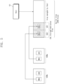
- FIG. 5 is a diagram describing an operation in which a computing system of FIG. 4 stores map data.
- components such as the host 101, the first CXL storage 120, the second CXL storage 130, and the CXL memory 110 are conceptually illustrated, and some unnecessary components are omitted.
- a partial area of the CXL memory 110 may be allocated for a dedicated area of the first and second CXL storages 120 and 130.
- the dedicated area of the first and second CXL storages 120 and 130 may include a mapping table that includes the first map data MD1 dedicated for the first CXL storage 120 and the second map data MD2 dedicated for the second CXL storage 130.
- the partial area of the CXL memory 110 may include a first dedicated area DA1 allocated to the first CXL storage 120 and a second dedicated area DA2 allocated to the second CXL storage 130.
- the first dedicated area DA1 allocated to the first CXL storage 120 may be accessed by the first CXL storage 120 and may be used to store the map data of the first CXL storage 120.
- the second dedicated area DA2 allocated to the second CXL storage 130 may be accessed by the second CXL storage 130 and may be used to store the map data of the second CXL storage 130.
- the nonvolatile memory NVMa of the first CXL storage 120 may store the first user data UD1 and the first map data MD1.
- the first CXL storage 120 may require a buffer area in which the first map data MD1 are to be stored.
- the first map data MD1 of the first CXL storage 120 may be stored in a partial area (e.g., the first dedicated area DA1) of the CXL memory 110.
- the first dedicated area DA1 of the CXL memory 110 may be accessed by the first CXL storage 120 through the CXL switch SW_CXL.
- the nonvolatile memory NVMb of the second CXL storage 130 may store second user data UD2 and the second map data MD2.
- the second map data MD2 of the second CXL storage 130 may be stored in a partial area (e.g., the second dedicated area DA2) of the CXL memory 110.
- the second dedicated area DA2 of the CXL memory 110 may be accessed by the second CXL storage 130 through the CXL switch SW_CXL.
- the remaining area of the CXL memory 110 which is not allocated, other than the dedicated area may be an area that is accessible by the host 101 or is managed by the host 101. In this case, the host 101 may access the remaining area of the CXL memory 110 through the CXL switch SW_CXL. In an embodiment, the remaining area of the CXL memory 110, which is not allocated for the dedicated area, may be used as a memory expander.
- FIG. 6 is a diagram describing an operation in which map data are stored in a CXL memory.
- the first map data MD1 present in the first CXL storage 120 and the second map data MD2 present in the second CXL storage 130 may be transferred and stored in the buffer memory BFM of the CXL memory 110 through a peer-to-peer (P2P) manner.
- P2P peer-to-peer
- the first CXL storage controller 121 of the first CXL storage 120 may include a direct memory access (DMA) engine.
- the DMA engine included in the first CXL storage controller 121 may transfer the first map data MD1 present in the nonvolatile memory NVMa to the CXL memory controller 111 without the interference or control of the host 101. That is, the map data may be transferred from the first CXL storage 120 to the CXL memory 110 based on the P2P manner.
- DMA direct memory access
- the second CXL storage controller 131 of the second CXL storage 130 may include a DMA engine.
- the DMA engine included in the second CXL storage controller 131 may transfer the second map data MD2 present in the nonvolatile memory NVMb to the CXL memory controller 111 without the interference or control of the host 101. That is, the map data may be transferred from the second CXL storage 130 to the CXL memory 110 based on the P2P manner.
- the above manners in which the map data are transferred from the first CXL storage 120 and the second CXL storage 130 to the CXL memory 110 are provided as an example, and the present disclosure is not limited thereto. It may be understood that the transfer of map data from the first CXL storage 120 and the second CXL storage 130 to the CXL memory 110 is implemented in various manners using the CXL interface or the CXL switch. In an embodiment, the transfer (i.e., the backup or flush) of map data from the CXL memory 110 to the first CXL storage 120 and the second CXL storage 130 may also be implemented in a manner(s) similar to the above manners.
- FIG. 7 is a flowchart illustrating a read operation for CXL storage of FIG. 2 .
- the read operation for the first CXL storage 120 according to the flowchart of FIG. 7 may be performed after the initialization operation of FIG. 4 is performed (i.e., after the first map data MD1 of the first CXL storage 120 are stored in the dedicated area of the CXL memory 110).
- the host 101 may send a first read request REQ_RD1 to the CXL memory 110 through the CXL host interface circuit 101a.
- the first read request REQ_RD1 may include a command indicating the read operation and a first logical block address LBA1. That is, the first read request REQ_RD1 may refer to a request for reading the first user data UD1 stored in the first CXL storage 120 and may include the first logical block address LBA1 corresponding to the first user data UD1.
- the CXL memory 110 may obtain a first physical block address PBA1 corresponding to the first logical block address LBA1 included in the first read request REQ_RD1.
- the CXL memory controller 111 of the CXL memory 110 may read the first map data MD1 from an area corresponding to a memory address (e.g., a logical address or a virtual address) included in the first read request REQ_RD1.
- the CXL memory controller 111 may read the first map data MD1 from the buffer memory BFM by using the buffer memory interface circuit 111f.
- the CXL memory controller 111 may obtain the first physical block address PBA1 corresponding to the first logical block address LBA1 with reference to the first map data MD1.
- the CXL memory 110 may send a second read request REQ_RD2 to the first CXL storage 120 through the CXL switch SW_CXL.
- the second read request REQ_RD2 may include a command indicating the read operation and the first physical block address PBA1.
- the first CXL storage 120 may read the first user data UD1 stored in an area of the nonvolatile memory NVMa, which corresponds to the first physical block address PBA1.
- the first CXL storage controller 121 may read the first user data UD1 from the area of the nonvolatile memory NVMa, which corresponds to the first physical block address PBA1.
- the first CXL storage controller 121 may read the first user data UD1 from the nonvolatile memory NVMa by using the NAND interface circuit 121d.
- the first CXL storage 120 may send a first read response REP_RD1 to the second read request REQ_RD2 through the CXL storage interface circuit 121a.
- the CXL switch SW_CXL may transfer the first read response REP_RD1 to the CXL memory 110.
- the first read response REP_RD1 may include the first user data UD1 requested through the second read request REQ_RD2 and the first physical block address PBA1.
- the CXL memory 110 may obtain the first logical block address LBA1 corresponding to the first physical block address PBA1 included in the first read response REP_RD1.
- the CXL memory controller 111 of the CXL memory 110 may read the first map data MD1 from an area corresponding to a memory address (e.g., a physical address or a virtual address) included in the first read response REP_RD1.
- the CXL memory controller 111 may read the first map data MD1 from the buffer memory BFM by using the buffer memory interface circuit 111f.
- the CXL memory controller 111 may obtain the first logical block address LBA1 corresponding to the first physical block address PBA1 with reference to the first map data MD1.
- the CXL memory 110 may send a second read response REP_RD2 to the host 101 through the CXL memory interface circuit 111a.
- the second read response REP_RD2 may include the first user data UD1 and the first logical block address LBA1.
- the read operation for the first CXL storage 120 is described with reference to FIG. 7 , but the read operation for the second CXL storage 130 may be performed in a manner similar to the above manner.
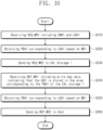
- FIG. 8 is a flowchart illustrating a read operation for CXL storage of FIG. 2 .
- An operating method in which the CXL memory 110 performs the read operation for the first CXL storage 120 will be described with reference to FIGS. 2 , 3 , and 8 .
- the CXL memory 110 may receive the first read request REQ_RD1 from the host 101 through the CXL memory interface circuit 111a.
- the first read request REQ_RD1 may include a command indicating the read operation and the first logical block address LBA1.
- the CXL memory 110 may obtain the first physical block address PBA1 corresponding to the first logical block address LBA1 included in the first read request REQ_RD1.
- the CXL memory controller 111 of the CXL memory 110 may obtain the first physical block address PBA1 corresponding to the first logical block address LBA1 with reference to the first map data MD1.
- the CXL memory 110 may send the second read request REQ_RD2 to the first CXL storage 120 through the CXL switch SW_CXL.
- the second read request REQ_RD2 may include a command indicating the read operation and the first physical block address PBA1.
- the CXL memory 110 may receive the first read response REP_RD1 from the first CXL storage 120.
- the first read response REP_RD1 may include the first user data UD1 requested through the second read request REQ_RD2 and the first physical block address PBA1.
- the CXL memory 110 may obtain the first logical block address LBA1 corresponding to the first physical block address PBA1 included in the first read response REP_RD1.
- the CXL memory controller 111 of the CXL memory 110 may obtain the first logical block address LBA1 corresponding to the first physical block address PBA1 with reference to the first map data MD1.
- the CXL memory 110 may send the second read response REP_RD2 to the host 101 through the CXL memory interface circuit 111a.
- the second read response REP_RD2 may include the first user data UD1 and the first logical block address LBA1.
- FIG. 9 is a flowchart illustrating a write operation for CXL storage of FIG. 2 .
- the write operation for the first CXL storage 120 according to the flowchart of FIG. 9 may be performed after the initialization operation of FIG. 4 is performed (i.e., after the first map data MD1 of the first CXL storage 120 are stored in the dedicated area of the CXL memory 110).
- the host 101 may send a first write request REQ_WR1 to the CXL memory 110 through the CXL host interface circuit 101a.
- the first write request REQ_WR1 may include a command indicating the write operation, the first logical block address LBA1 and the first user data UD1. That is, the first write request REQ_WR1 may refer to a request for writing the first user data UD1 in a CXL storage and may include the first logical block address LBA1 corresponding to the first user data UD1. All or part of the first user data UD1 may be temporarily stored in the buffer memory BFM of the CXL memory 110.
- the CXL memory 110 may obtain the first physical block address PBA1 corresponding to the first logical block address LBA1 included in the first write request REQ_WR1.
- the CXL memory 110 may determine CXL storage in which the first user data UD1 are to be written, in response to the first write request REQ_WR1.
- the CXL memory 110 may select CXL storage in which the first user data UD1 are to be written, in consideration of the capacity of each of the first CXL storage 120 and the second CXL storage 130.
- the FTL 111d of the CXL memory 110 may manage block information about a memory block, which is free, capable of being written, or capable of being allocated, from among memory blocks included in a nonvolatile memory of the selected CXL storage.
- the FTL 111d may select a memory block of the CXL storage, in which the first user data UD1 are to be written, based on the block information. That is, the first physical block address PBA1 may refer to a physical address of a memory block of the CXL storage selected by the CXL memory 110 to write the first user data UD1.
- the CXL memory 110 may send a second write request REQ_WR2 to the first CXL storage 120 through the CXL switch SW_CXL.
- the second write request REQ_WR2 may include a command indicating the write operation, the first physical block address PBA1 and the first user data UD1.
- the first CXL storage 120 may write the first user data UD1 in the selected memory block.
- the first CXL storage controller 121 may control the nonvolatile memory NVMa such that the first user data UD1 are written in the selected memory block.
- the first CXL storage controller 121 may write the first user data UD1 in the nonvolatile memory NVMa by using the NAND interface circuit 121d.
- the first CXL storage 120 may generate write map data.
- the write map data may include information indicating that the first user data UD1 corresponding to the first logical block address LBA1 are stored in the first CXL storage 120 as a result of the selection in the second operation 2.
- the first CXL storage 120 may send a first write response REP_WR1 to the second write request REQ_WR2 through the CXL storage interface circuit 121a.
- the CXL switch SW_CXL may transfer the first write response REP_WR1 to the CXL memory 110.
- the first write response REP_WR1 may include the write map data and the first physical block address PBA1.
- the CXL memory 110 may obtain the first logical block address LBA1 corresponding to the first physical block address PBA1 included in the first write response REP_WR1.
- the CXL memory 110 may update the first map data MD1 based on the write map data.
- the first map data MD1 may further include an attribute indicating the CXL storage in which the first user data UD1 is written, and the CXL memory 110 may update the attributes corresponding to the first logical block address LBA1 and the first physical block address PBA1 such that the attribute indicates the first CXL storage 120, based on the write map data.
- the CXL memory 110 may obtain the first logical block address corresponding to the first physical block address PBA1 based on the updated first map data MD1.
- the CXL memory 110 may send a second write response REP_WR2 to the host 101 through the CXL memory interface circuit 111a.
- the second write response REP_WR2 may include the updated first logical block address.
- the host 101 may determine that the first user data UD1 corresponding to the first write request REQ_WR1 are normally stored.
- the write operation for the first CXL storage 120 is described with reference to FIG. 9 , but the write operation for the second CXL storage 130 may also be performed in a manner similar to the above manner.
- FIG. 10 is a flowchart illustrating a write operation for CXL storage of FIG. 2 .
- An operating method in which the CXL memory 110 performs the write operation for the first CXL storage 120 will be described with reference to FIGS. 2 , 3 , and 10 .
- the CXL memory 110 may receive the first write request REQ_WR1 from the host 101 through the CXL memory interface circuit 111a.
- the first write request REQ_WR1 may include a command indicating the write operation and the first logical block address LBA1.
- the CXL memory 110 may obtain the first physical block address PBA1 corresponding to the first logical block address LBA1 included in the first write request REQ_WR1.
- the CXL memory controller 111 of the CXL memory 110 may determine CXL storage where the first user data UD1 are to be written, in response to the first write request REQ_WR1.
- the CXL memory 110 may send the second write request REQ_WR2 to the first CXL storage 120 through the CXL switch SW_CXL.
- the second write request REQ_WR2 may include a command indicating the write operation and the first physical block address PBA1.
- the CXL memory 110 may receive the first write response REP_WR1 from the first CXL storage 120.
- the first write response REP_WR1 may include write map data and the first physical block address PBA1.
- the CXL memory 110 may obtain the first logical block address LBA1 corresponding to the first physical block address PBA1 included in the first write response REP_WR1. In an embodiment, the CXL memory 110 may update the first map data MD1 based on the write map data.
- the CXL memory 110 may send the second write response REP_WR2 to the host 101 through the CXL memory interface circuit 111a.
- the second write response REP_WR2 may include the updated first logical block address LBA1.
- FIG. 11 is a flowchart describing a power-off operation of a computing system of FIG. 2 .
- FIG. 11 is a flowchart illustrating a power-off operation of a computing system of FIG. 2 .
- a power-off operation of a computing system will be described with reference to FIG. 11 , but the present disclosure is not limited thereto.
- the operating method of FIG. 11 is applicable to the power-off operation or reset operation of each of various components (e.g., a host, CXL storage, a CXL memory, and a CXL switch) included in the computing system.
- various components e.g., a host, CXL storage, a CXL memory, and a CXL switch
- the CXL memory 110 may output first power-off information IFM_off1 and second power-off information IFM_off2 to the CXL switch SW_CXL through the CXL memory interface circuit 111a.
- the CXL switch SW_CXL may transfer the power-off information IFM_off to the first CXL storage 120.
- the CXL memory 110 may send the first power-off information IFM_off1, which allows the first CXL storage 120 to perform the power-off operation, to the first CXL storage 120 through the CXL switch SW_CXL.
- the CXL memory 110 may send the second power-off information IFM_off2, which allows the second CXL storage 130 to perform the power-off operation, to the second CXL storage 130 through the CXL switch SW_CXL.
- the first CXL storage 120 may output the first read request REQ_RD1 through the CXL storage interface circuit 121a in response to the first power-off information IFM_off1.
- the CXL switch SW_CXL may transfer the first read request REQ_RD1 to the CXL memory 110.
- the first read request REQ_RD1 in operation POF-S21 may refer to a request for reading the first map data MD1 stored in the CXL memory 110.
- the first read request REQ_RD1 may include a memory address of an area where the first map data MD1 are stored.
- the CXL memory 110 may read the first map data MD1 in response to the first read request REQ_RD1. For example, the CXL memory 110 may read the first map data MD1 from the buffer memory BFM based on the memory address included in the first read request REQ_RD1.
- the second CXL storage 130 may output the second read request REQ_RD2 through the CXL storage interface circuit 131a in response to the second power-off information IFM_off2.
- the CXL switch SW_CXL may transfer the second read request REQ_RD2 to the CXL memory 110.
- the second read request REQ_RD2 in operation POF-S22 may refer to a request for reading the second map data MD2 stored in the CXL memory 110.
- the second read request REQ_RD2 may include a memory address of an area where the second map data MD2 are stored.
- the CXL memory 110 may read the second map data MD2 in response to the second read request REQ_RD2.
- the CXL memory 110 may read the second map data MD2 from the buffer memory BFM based on the memory address included in the second read request REQ_RD2.
- operation POF-S22 is performed after operation POF-S21 is illustrated, but the present disclosure is not limited thereto.
- operation POF-S21 may be performed after operation POF-S22, or operation POF-S21 and operation PUP-S22 may be simultaneously performed.
- the CXL memory 110 may output the first read response REP_RD1 to the first read request REQ_RD1 through the CXL memory interface circuit 111a.
- the CXL switch SW_CXL may transfer the first read response REP_RD1 to the first CXL storage 120.
- the CXL memory 110 may output the second read response REP_RD2 to the second read request REQ_RD2 through the CXL memory interface circuit 111a.
- the CXL switch SW_CXL may transfer the second read response REP_RD2 to the second CXL storage 130.
- the first CXL storage 120 may write the first map data MD1 included in the first read response REP_RD1 in the nonvolatile memory NVMa. In an embodiment, the first CXL storage 120 may store the first map data MD1 in a given area of the nonvolatile memory NVMa.
- the second CXL storage 130 may write the second map data MD2 included in the second read response REP_RD2 in the nonvolatile memory NVMb. In an embodiment, the second CXL storage 130 may store the second map data MD2 in a given area of the nonvolatile memory NVMb.
- the first CXL storage 120 may output a first response ACK_off1 to the first power-off information IFM_off1.
- the CXL switch SW_CXL may send the first response ACK_off1 to the CXL memory 110.
- the CXL memory 110 may recognize that the first map data MD1 present in the CXL memory 110 are normally stored in the first CXL storage 120, based on the first response ACK_off1.
- the second CXL storage 130 may output a second response ACK_off2 to the second power-off information IFM_off2.
- the CXL switch SW_CXL may send the second response ACK_off2 to the CXL memory 110.
- the CXL memory 110 may recognize that the second map data MD2 present in the CXL memory 110 are normally stored in the second CXL storage 130, based on the second response ACK_off2.
- the first CXL storage 120, the second CXL storage 130, the CXL memory 110, and the CXL switch SW_CXL may be powered off.
- the CXL memory 110 may send a power interruption request to the host 101; based on the power interruption request, the host 101 may interrupt the power that is supplied to the first CXL storage 120, the second CXL storage 130, the CXL memory 110, and the CXL switch SW_CXL.
- the operation for the first CXL storage 120 is performed prior to the operation for the second CXL storage 130 is illustrated, but the present disclosure is not limited thereto.
- the operation for the first CXL storage 120 may be performed after the operation for the second CXL storage 130, or the operation for the first CXL storage 120 and the operation for the second CXL storage 130 may be simultaneously performed.
- the power-off operation described with reference to FIG. 11 is provided as an example, and the present disclosure is not limited thereto.
- the CXL memory 110 may provide notification that the first map data MD1 and the second map data MD2 are completely backed up, by sending the first response ACK_off1 and the second response ACK_off2 to the host 11 (i.e., an interrupt manner).
- the first CXL storage 120 may store the first map data MD1 present in the CXL memory 110 in the nonvolatile memory NVMa and may then set a value of a specific register to a given value.
- the host 101 may determine whether the first map data MD1 are completely backed up, by periodically checking the value of the specific register through the CXL memory 110 (i.e., a polling manner).
- the first CXL storage 120 may be configured to complete the backup operation for the first map data MD1 within a given time from a point in time when the first power-off information IFM_off1 is received from the CXL memory 110 (i.e., a time-out manner).
- the first CXL storage 120 may transfer information, which indicates that the first map data MD1 are completely backed up, to the host 101 through the CXL memory 110 by using at least one of the above manners.
- FIG. 12 is a block diagram illustrating a computing system according to an embodiment of the present disclosure. For convenience of description, additional description associated with the components described above will be omitted to avoid redundancy.
- a computing system 1000 may include a first CPU 1110, a second CPU 1120, a CPU 1130, an NPU 1140, the CXL switch SW_CXL, CXL storage 1210, a CXL memory 1220, a PCIe device 1310, and an accelerator (CXL device) 1320.
- the first CPU 1110, the second CPU 1120, the CPU 1130, the NPU 1140, the CXL storage 1210, the CXL memory 1220, the PCIe device 1310, and the accelerator (CXL device) 1320 may be connected in common with the CXL switch SW_CXL and may communicate with each other through the CXL switch SW_CXL.
- each of the first CPU 1110, the second CPU 1120, the CPU 1130, and the NPU 1140 may be the host described with reference to FIGS. 1 to 12 and may be directly connected with individual memory devices.
- the CXL storage 1210 and the CXL memory 1220 may be the CXL storage and the CXL memory described with reference to FIGS. 2 to 12 , and at least a partial area of the CXL memory 1220 may be allocated for an area dedicated for the CXL storage 1210 by one or more of the first CPU 1110, the second CPU 1120, the CPU 1130, and the NPU 1140. That is, the CXL storage 1210 and the CXL memory 1220 may be used as a storage space STR of the computing system 1000.
- the CXL switch SW_CXL may be connected with the PCIe device 1310 or the accelerator 1320 configured to support various functions, and the PCIe device 1310 or the accelerator 1320 may communicate with each of the first CPU 1110, the second CPU 1120, the GPU 1130, and the NPU 1140 through the CXL switch SW_CXL or may access the storage space STR including the CXL storage 1210 and the CXL memory 1220 through the CXL switch SW_CXL.
- the CXL switch SW_CXL may be connected with an external network or Fabric and may be configured to communicate with an external server through the external network or Fabric.
- FIG. 13 is a block diagram illustrating a data center to which a computing system according to an embodiment of the present disclosure is applied.
- a data center 2000 that is a facility collecting various data and sending services may be referred to as a "data storage center”.
- the data center 2000 may be a system for operating a search engine and a database, and may be a computing system used in a business such as a bank or in a government institution.
- the data center 2000 may include application servers 2110 to 21m0 and storage servers 2210 to 22n0.
- the number of application servers and the number of storage servers may be variously selected depending on an embodiment, and the number of application servers and the number of storage servers may be different from each other.
- the application servers 2110 to 21m0 may have similar structures, the storage servers 2210 to 22n0 may have similar structures, and the application servers 2110 to 21m0 and the storage servers 2210 to 22n0 may communicate with each other over a network NT.
- the first storage server 2210 may include a processor 2211, a memory 2212, a switch 2213, a storage device 2215, a CXL memory 2214, and a network interface card (NIC) 2216.
- the processor 2211 may control an overall operation of the first storage server 2210 and may access the memory 2212 to execute an instruction loaded onto the memory 2212 or to process data.
- the memory 2212 may be implemented with a DDR SDRAM (Double Data Rate Synchronous DRAM), an HBM (High Bandwidth Memory), an HMC (Hybrid Memory Cube), a DIMM (Dual In-line Memory Module), an Optane DIMM, and/or an NVMDIMM (Non-Volatile DIMM).
- the processor 2211 and the memory 2212 may be directly connected, and the numbers of processors and memories included in one storage server 2210 may be variously selected.
- the processor 2211 and the memory 2212 may form a processor-memory pair. In an embodiment, the number of processors 2211 and the number of memories 2212 may be different from each other.
- the processor 2211 may include a single core processor or a multi-core processor.
- the detailed description of the storage server 2210 may be similarly applied to the application servers 2110 to 21m0.
- the switch 2213 may be configured to arbitrate or route the communications between various components included in the first storage server 2210.
- the switch 2213 may be implemented with the CXL switch SW_CXL described with reference to FIGS. 1 to 12 . That is, the switch 2213 may be a switch implemented based on the CXL protocol.
- the CXL memory 2214 may be connected with the switch 2213.
- the CXL memory 2214 may be used as a memory expander for the processor 2211.
- the CXL memory 2214 may be allocated for a dedicated memory or a buffer memory of the storage device 2215.
- the storage device 2215 may include a CXL interface circuit CXL_IF, a controller CTRL, and a NAND flash NAND. Depending on a request of the processor 2211, the storage device 2215 may store data or may output the stored data. In an embodiment, the storage device 2215 may be implemented with the first CXL storage described with reference to FIGS. 1 to 12 . In an embodiment, as in the description given with reference to FIGS. 1 to 12 , at least a partial area of the CXL memory 2214 may be allocated for a dedicated area, and the dedicated area may be used as a buffer memory (i.e., may be used to store map data in the CXL memory 2214).
- the first storage server 2210 may include a plurality of storage devices.
- at least a partial area of the CXL memory 2214 may be allocated for a dedicated area of each of the plurality of storage devices, and the dedicated area of each of the plurality of storage devices may be used as a buffer memory of each of the plurality of storage devices.
- the application servers 2110 to 21m0 may not include the storage device 2215.
- the storage server 2210 may include at least one or more storage devices 2215.
- the number of storage devices 2215 included in the storage server 2210 may be variously selected depending on an embodiment.
- the NIC 2216 may be connected with the CXL switch SW_CXL.
- the NIC 2216 may communicate with the remaining storage servers 2220 to 22n0 or the application servers 2210 to 21m0 over the network NT.
- the NIC 2216 may include a network interface card, a network adapter, etc.
- the NIC 2216 may be connected with the network NT by a wired interface, a wireless interface, a Bluetooth interface, an optical interface, etc.
- the NIC 2216 may include an internal memory, a digital signal processor (DSP), a host bus interface, etc. and may be connected with the processor 2211 and/or the switch 2213 through the host bus interface.
- the NIC 2216 may be integrated with at least one of the processor 2211, the switch 2213, and the storage device 2215.
- the network NT may be implemented by using a Fibre channel (FC) or an Ethernet.
- FC Fibre channel
- Ethernet may be a medium that is used in high-speed data transmission and may use an optical switch that sending high performance/high availability.
- Storage servers may be provided as file storage, block storage, or object storage depending on an access manner of the network NT.
- the network NT may be a storage-dedicated network such as a storage area network (SAN).
- the SAN may be a FC-SAN that uses a FC network and is implemented depending on a FC protocol (FCP).
- FCP FC protocol
- the SAN may be an IP-SAN that uses a TCP/IP network and is implemented depending on an iSCSI (SCSI over TCP/IP or Internet SCSI).
- the network NT may be a legacy network such as a TCP/IP network.
- the network NT may be implemented depending on the following protocol: FCoE (FC over Ethernet), NAS (Network Attached Storage), or NVMe-oF (NVMe over Fabrics).
- At least one of the application servers 2110 to 21m0 may store data, which are store-requested by a user or a client, in one of the storage servers 2210 to 22n0 over the network NT. At least one of the application servers 2110 to 21m0 may obtain data, which are read-requested by the user or the client, from one of the storage servers 2210 to 22n0 over the network NT.
- at least one of the application servers 2110 to 21m0 may be implemented with a web server, a database management system (DBMS), etc.
- DBMS database management system
- At least one of the application servers 2110 to 21m0 may access a memory, a CXL memory, or a storage device included in any other application server over the network NT or may access memories, CXL memories, or storage devices included in the storage servers 2210 to 22n0 over the network NT.
- at least one of the application servers 2110 to 21m0 may perform various operations on data stored in the remaining application servers and/or storage servers.
- at least one of the application servers 2110 to 21m0 may execute an instruction for moving or copying data between the remaining application servers and/or storage servers.
- the data may be moved from storage devices of storage servers to memories or CXL memories of application servers through memories or CXL memories of the storage servers or directly.
- the data that are transferred over a network may be data that are encrypted for security or privacy.
- a CXL memory included in at least one of the application servers 2110 to 21m0 and the storage servers 2210 to 22n0 may be allocated for a dedicated area of a storage device included in at least one of the application servers 2110 to 21m0 and the storage servers 2210 to 22n0, and the storage device may use the dedicated area thus allocated as a buffer memory (i.e., may store map data in the dedicated area).
- a CXL memory included in a storage server (e.g., 22n0) may be allocated to the storage device 2215 included in the storage server 2210, and the storage device 2215 included in the storage server 2210 may access the CXL memory included in the storage server (e.g., 22n0) over the switch 2213 and the NIC 2216.
- the map data associated with the storage device 2215 of the first storage server 2210 may be stored in the CXL memory of the storage server 22n0. That is, storage devices and CXL memories of a data center according to the present disclosure may be connected and implemented in various manners.
- a memory device managing map data of each of a plurality of storage devices and an operating method thereof are provided.
- the plurality of storage devices are connected with a memory device in a cascade structure without the connection with a host
- storage devices the number of which is more than the number of storage devices capable of being connected with an existing host, may be connected. Accordingly, a high-capacity computing system may be implemented.
Abstract
An operating method of a memory device which communicates with a first storage device and a second storage device through an interface circuit is provided. The method includes receiving, from a host device, a first request including a command and a first logical block address; obtaining, based on the first logical block address, a first physical block address with reference to first map data dedicated for the first storage device; and sending, to the first storage device through the interface circuit, a second request including the first physical block address and the command.
Description
- This application claims priority under 35 U.S.C. § 119 to
Korean Patent Application No. 10-2022-0056187 filed on May 6, 2022 - Embodiments of the present disclosure described herein relate to a memory device, and more particularly, relate to a memory device managing map data of each of a plurality of storage devices.
- A memory device stores data in response to a write request and outputs data stored therein in response to a read request. For example, the memory device is classified as a volatile memory device, which loses data stored therein when a power supply is interrupted, such as a dynamic random access memory (DRAM) device, a static RAM (SRAM) device, or a nonvolatile memory device, which retains data stored therein even when a power supply is interrupted, such as a flash memory device, a phase-change RAM (PRAM), a magnetic RAM (MRAM), or a resistive RAM (RRAM). The nonvolatile memory device may be used as a storage device storing a large amount of data.
- In the related art, the number of storage devices capable of being connected with a host may be limited depending on an interface of the host. As such, it is difficult to implement a high-capacity solid state drive (SSD). That is, an SSD device including a plurality of storage devices may be required regardless of the limitation on the number of storage devices capable of being connected with the host.
- Embodiments of the present disclosure provide an operating method of a memory device managing map data of each of a plurality of storage devices, a computing system including the memory device, and an operating method of the computing system.
- According to an aspect of an example embodiment, there is provided an operating method of a memory device which communicates with a first storage device and a second storage device through an interface circuit, the operating method including: receiving, from a host device, a first request including a command and a first logical block address; obtaining, based on the first logical block address, a first physical block address with reference to first map data dedicated for the first storage device; and sending, to the first storage device through the interface circuit, a second request including the first physical block address and the command.
- According to an aspect of an example embodiment, there is provided a computing system including: a first storage device; a second storage device; a memory device storing a mapping table for managing first map data dedicated for the first storage device and second map data dedicated for the second storage device; and an interface circuit configured to communicate with the first storage device, the second storage device, and the memory device, wherein the memory device is configured to: receive, from a host device, a first request including a command and a first logical block address, obtain, based on the first logical block address, a first physical block address with reference to the first map data of the mapping table, and send, to the first storage device through the interface circuit, a second request including the first physical block address and the command.
- According to an aspect of an example embodiment, there is provided an operating method of a computing system which includes a first storage device, a second storage device, a memory device, and an interface circuit communicating with the first storage device, the second storage device, and the memory device, the operating method including: receiving, by the memory device, a first request including a command and a first logical block address from a host device; obtaining, by the memory device, a first physical block address with reference to first map data dedicated for the first storage device, based on the first logical block address; and sending, by the memory device, a second request including the first physical block address and the command to the first storage device through the interface circuit.
- The above and other aspects and features of the present disclosure will become apparent by describing in detail embodiments thereof with reference to the accompanying drawings, in which:
-
FIG. 1 is a block diagram of a computing system including a storage device; -
FIG. 2 is a block diagram of a computing system to which a storage device is applied; -
FIG. 3 is a block diagram illustrating a computing system ofFIG. 2 ; -
FIG. 4 is a flowchart describing an initialization operation or a power-up operation of a computing system ofFIG. 3 ; -
FIG. 5 is a diagram describing an operation in which a computing system ofFIG. 4 stores map data; -
FIG. 6 is a diagram describing an operation in which map data are stored in a CXL memory; -
FIG. 7 is a flowchart illustrating a read operation for CXL storage ofFIG. 2 ; -
FIG. 8 is a flowchart illustrating a read operation for CXL storage ofFIG. 2 ; -
FIG. 9 is a flowchart illustrating a write operation for CXL storage ofFIG. 2 ; -
FIG. 10 is a flowchart illustrating a write operation for CXL storage ofFIG. 2 ; -
FIG. 11 is a flowchart illustrating a power-off operation of a computing system ofFIG. 2 ; -
FIG. 12 is a block diagram of a computing system according to an embodiment of the present disclosure; and -
FIG. 13 is a block diagram of a computing system according to an embodiment of the present disclosure. - Below, embodiments of the present disclosure will be described in detail and clearly to such an extent that one skilled in the art implements embodiment of the present disclosure easily. With regard to the description of the present disclosure, to make the overall understanding easy, like components will be marked by like reference signs/numerals in drawings, and thus, additional description will be omitted to avoid redundancy.
-
FIG. 1 is a block diagram illustrating a computing system including a storage device. Referring toFIG. 1 , acomputing system 10 may include ahost 11, a plurality ofmemory devices storage device 13. Thehost 11 may control an overall operation of thecomputing system 10. The plurality ofmemory devices host 11. - The
storage device 13 may include astorage controller 13a, abuffer memory 13b, and anonvolatile memory 13c. Under control of thehost 11, thestorage controller 13a may store data in thenonvolatile memory 13c or may send data stored in thenonvolatile memory 13c to thehost 11. - The
buffer memory 13b may store a variety of information necessary for thestorage device 13 to operate. For example, thestorage controller 13a may manage data stored in thenonvolatile memory 13c by using map data. The map data may include information about relationship between a logical block address managed by thehost 11 and a physical block address of thenonvolatile memory 13c. - In an embodiment, the
buffer memory 13b may be a high-speed memory such as a DRAM. As the capacity of thenonvolatile memory 13c increases, the size of necessary map data may increase. However, because the capacity of thebuffer memory 13b included in thesingle storage device 13 is limited, it is impossible to cope with the increase in the size of the map data due to the increase in the capacity of thenonvolatile memory 13c. -
FIG. 2 is a block diagram illustrating a computing system to which a storage system according to an embodiment of the present disclosure is applied. Referring toFIG. 2 , acomputing system 100 may include ahost 101, a plurality ofmemory devices storage 120,second CXL storage 130, and aCXL memory 110. In an embodiment, thecomputing system 100 may be included in user devices such as a personal computer, a laptop computer, a server, a media player, and a digital camera or automotive devices such as a navigation system, a black box, and an automotive electronic device/part. Alternatively, thecomputing system 100 may be a mobile system such as a mobile phone, a smartphone, a tablet personal computer (PC), a wearable device, a health care device, or an Internet of things (IoT) device. - The
host 101 may control an overall operation of thecomputing system 100. In an embodiment, thehost 101 may be one of various processors such as a central processing unit (CPU), a graphics processing unit (GPU), a neural processing unit (NPU), and a data processing unit (DPU). In an embodiment, thehost 101 may include a single core processor or a multi-core processor. - The plurality of
memory devices computing system 100. In an embodiment, each of the plurality ofmemory devices memory devices - The plurality of
memory devices host 101 through the DDR interface. In an embodiment, thehost 101 may include a memory controller configured to control the plurality ofmemory devices memory devices host 101 through various interfaces. - The
first CXL storage 120 may include a firstCXL storage controller 121 and a nonvolatile memory NVMa. Under control of thehost 101, the firstCXL storage controller 121 may store data in the nonvolatile memory NVMa or may send data stored in the nonvolatile memory NVMa to thehost 101. In an embodiment, the nonvolatile memory NVMa may be a NAND flash memory, but the present disclosure is not limited thereto. - The
second CXL storage 130 may include a secondCXL storage controller 131 and a nonvolatile memory NVMb. Under control of thehost 101, the secondCXL storage controller 131 may store data in the nonvolatile memory NVMb or may send data stored in the nonvolatile memory NVMb to thehost 101. In an embodiment, thesecond CXL storage 130 may be connected with thefirst CXL storage 120 in a cascade structure. - The
CXL memory 110 may include aCXL memory controller 111 and a buffer memory BFM. Under control of thehost 101, theCXL memory controller 111 may store data in the buffer memory BFM or may send data stored in the buffer memory BFM to thehost 101. In an embodiment, the buffer memory BFM may be a DRAM, but the present disclosure is not limited thereto. - In an embodiment, the
first CXL storage 120, thesecond CXL storage 130, and theCXL memory 110 may be configured to share the same interface. For example, thefirst CXL storage 120, thesecond CXL storage 130, and theCXL memory 110 may communicate with each other through a CXL interface IF_CXL. In an embodiment, the CXL interface IF_CXL may indicate a low-latency and high-bandwidth link that supports coherency, memory access, and dynamic protocol muxing of IO protocols such that various connections between accelerators, memory devices, or various electronic devices are possible. - In an embodiment, unlike the
storage device 13 ofFIG. 1 , each of thefirst CXL storage 120 and thesecond CXL storage 130 may not include a separate buffer memory for storing or managing map data. In this case, each of thefirst CXL storage 120 and thesecond CXL storage 130 may require a buffer memory for storing or managing the map data. In an embodiment, at least a partial area of theCXL memory 110 may be used as a buffer memory of each of thefirst CXL storage 120 and thesecond CXL storage 130. - In this case, a mapping table for managing map data dedicated for the
first CXL storage 120 and map data dedicated for thesecond CXL storage 130 may be stored in theCXL memory 110. For example, at least a partial area of theCXL memory 110 may be allocated for a buffer memory of the first CXL storage 120 (i.e., for an area dedicated for the first CXL storage 120) by thehost 101. - In an embodiment, the
first CXL storage 120 may access theCXL memory 110 through the CXL interface IF_CXL. For example, thefirst CXL storage 120 may store the mapping table in the allocated area of theCXL memory 110 or may read the mapping table from the allocated area of theCXL memory 110. Under control of thefirst CXL storage 120, theCXL memory 110 may store data (e.g., the map data) in the buffer memory BFM or may send the data (e.g., the map data) stored in the buffer memory BFM to thefirst CXL storage 120. - In an embodiment, as in the
first CXL storage 120, thesecond CXL storage 130 may access theCXL memory 110 through the CXL interface IF_CXL. For example, thesecond CXL storage 130 may store the mapping table in the allocated area of theCXL memory 110 or may read the mapping table from the allocated area of theCXL memory 110. Under control of thesecond CXL storage 130, theCXL memory 110 may store data (e.g., the map data) in the buffer memory BFM or may send the data (e.g., the map data) stored in the buffer memory BFM to thesecond CXL storage 130. - As described with reference to
FIG. 1 , the relatedart storage device 13 stores and manages the map data by using thebuffer memory 13b included therein. As the capacity of thestorage device 13 increases, the size of the map data increase, thereby causing an increase in the capacity of thebuffer memory 13b included in thestorage device 13. However, there is a limitation on an increase in capacity due to the structure and physical characteristic of thebuffer memory 13b included in thestorage device 13; in this case, the design change or additional integration of thebuffer memory 13b is required. - In contrast, according to an embodiment of the present disclosure, the
first CXL storage 120 may use at least a partial area of theCXL memory 110 placed outside thefirst CXL storage 120 as a buffer memory. Also, thesecond CXL storage 130 may use at least a partial area of theCXL memory 110 placed outside thesecond CXL storage 130 as a buffer memory. In this case, because theCXL memory 110 is implemented independently of thefirst CXL storage 120 and thesecond CXL storage 130, theCXL memory 110 may be implemented with a high-capacity memory. As such, even though the size of the map data increases due to an increase in the capacity of thefirst CXL storage 120 and thesecond CXL storage 130, the map data may be normally managed by theCXL memory 110. - In an embodiment, the
storage controller 13a of the relatedart storage device 13 communicates with thehost 11 through the host interface such as PCIe or NVMe, and communicates with thebuffer memory 13b through the memory interface such as a DDR interface or an LPDDR interface. That is, thestorage controller 13a of the relatedart storage device 13 communicates with thehost 11 and thebuffer memory 13b included therein, through different interfaces (i.e., heterogeneous interfaces). - In contrast, according to an embodiment of the present disclosure, the first
CXL storage controller 121 of thefirst CXL storage 120 may communicate with the CXL memory 110 (i.e., a buffer memory) through the CXL interface IF_CXL, the secondCXL storage controller 131 of thesecond CXL storage 130 may communicate with the CXL memory 110 (i.e., a buffer memory) through the CXL interface IF_CXL, and theCXL memory 110 may communicate with thehost 101 through an interface different from the CXL interface IF _CXL. In other words, each of the firstCXL storage controller 121 and the secondCXL storage controller 131 may communicate with theCXL memory 110 through a homogeneous interface or a common interface and may use a partial area of theCXL memory 110 as a buffer memory. - Below, for convenience of description, it is assumed that the
first CXL storage 120, thesecond CXL storage 130, and theCXL memory 110 communicate with each other through the CXL interface IF_CXL. However, the present disclosure is not limited thereto. For example, thefirst CXL storage 120, thesecond CXL storage 130, and theCXL memory 110 may communicate with each other based on various computing interfaces complying with the following: GEN-Z protocol, NVLink protocol, CCIX protocol, and Open CAPI protocol. - Also, for convenience of illustration, an example where the
CXL memory 110 communicates with thefirst CXL storage 120 and thesecond CXL storage 130 through the CXL interface IF_CXL is illustrated, but the present disclosure is not limited thereto. For example, theCXL memory 110 may communicate with two or more CXL storages through the CXL interface IF_CXL. That is, theCXL memory 110 and the plurality of CXL storages may be connected through the CXL interface IF_CXL in the cascade structure. -
FIG. 3 is a block diagram illustrating components of a computing system ofFIG. 2 in detail. Referring toFIGS. 2 and3 , thecomputing system 100 may include a CXL switch SW_CXL, thehost 101, thefirst CXL storage 120, thesecond CXL storage 130, and theCXL memory 110. - The CXL switch SW_CXL may be a component included in the CXL interface IF_CXL. The CXL switch SW_CXL may be configured to arbitrate the communications between the
first CXL storage 120, thesecond CXL storage 130, and theCXL memory 110. For example, in the case of storing data in thefirst CXL storage 120, the CXL switch SW_CXL may be configured to send information, which is provided from theCXL memory 110, such as a request, data, a response, or a signal, to thefirst CXL storage 120. In the case of storing data in thesecond CXL storage 130, the CXL switch SW_CXL may be configured to send information, which is provided from theCXL memory 110, such as a request, data, a response, or a signal, to thesecond CXL storage 130. - The
host 101 may include a CXLhost interface circuit 101a. The CXLhost interface circuit 101a may communicate with theCXL memory 110. - In an embodiment, a configuration of the
first CXL storage 120 may be different from configurations of related art storages. For example, a related art storage device (e.g., an SSD including a DRAM buffer) stores and manages map data in the DRAM buffer included in the related art storage device. In this case, a high-capacity DRAM buffer for storing the map data should be included in the related art storage device. Alternatively, another type of related art storage device (e.g., a DRAM-less SSD or a DRAM-less memory card) stores the entire map data in a nonvolatile memory (e.g., a NAND flash memory) included in the related art storage device and loads and uses a portion of the map data onto an SRAM buffer. In this case, to load the map data, the access to the nonvolatile memory whose operating speed is lower than that of the DRAM buffer is frequently performed, thereby reducing the performance of operation. - In contrast, each of the
first CXL storage 120 and thesecond CXL storage 130 according to the present disclosure may not include a separate DRAM buffer configured to store the map data. In this case, each of the map data of thefirst CXL storage 120 and the map data of thesecond CXL storage 130 may be stored and managed in theCXL memory 110 placed outside thefirst CXL storage 120 and thesecond CXL storage 130. As will be described below, because theCXL memory 110 supports a fast operating speed, thefirst CXL storage 120 and thesecond CXL storage 130 may have the same performance as the related art storage device (e.g., a storage device including a DRAM). In addition, because theCXL memory 110 are placed outside thefirst CXL storage 120 and thesecond CXL storage 130, it may be possible to easily cope with a large amount of map data of each of thefirst CXL storage 120 and thesecond CXL storage 130. - The
first CXL storage 120 may include the firstCXL storage controller 121 and the nonvolatile memory NVMa. The firstCXL storage controller 121 may include a CXLstorage interface circuit 121a, aprocessor 121b, aRAM 121c, and aNAND interface circuit 121d. - The CXL
storage interface circuit 121a may be connected with the CXL switch SW _CXL. The CXLstorage interface circuit 121a may communicate with theCXL memory 110 through the CXL switch SW_CXL. - The
processor 121b may be configured to control an overall operation of the firstCXL storage controller 121. TheRAM 121c may be used as a working memory or a buffer memory of the firstCXL storage controller 121. In an embodiment, theRAM 121c may be an SRAM and may be used as a read buffer and a write buffer for thefirst CXL storage 120. In an embodiment, as will be described below, theRAM 121c may be configured to temporarily store first map data MD1 read from theCXL memory 110 or a portion of the first map data MD1. - The
NAND interface circuit 121d may control the nonvolatile memory NVMa such that data are stored in the nonvolatile memory NVMa or data are read from the nonvolatile memory NVMa. In an embodiment, theNAND interface circuit 121d may be implemented to comply with the standard protocol such as a toggle interface or ONFI. For example, the nonvolatile memory NVMa may include a plurality of NAND flash devices; in the case where theNAND interface circuit 121d is implemented based on the toggle interface, theNAND interface circuit 121d communicates with the plurality of NAND flash devices through a plurality of channels. The plurality of NAND flash devices may be connected with the plurality of channels through a multi-channel, multi-way structure. - The
NAND interface circuit 121d may send a chip enable signal /CE, a command latch enable signal CLE, an address latch enable signal ALE, a read enable signal /RE and a write enable signal /WE to the plurality of NAND flash devices through the plurality of channels. TheNAND interface circuit 121d and the plurality of NAND flash devices may exchange a data signal DQ and a data strobe signal DQS through the plurality of channels.[Table 1] /CE CLE ALE /WE /RE DQS DQx MODE L H L ↑ H X CMD Command Input L L H ↑ H X ADDR Address Input L L L H H ↑↓ DATA_in Data Input L L L H ↑↓ ↑↓ DATA_out Data Output - Table 1 shows operating modes of a NAND flash device according to a state of each signal. Referring to Table 1, while the NAND flash device receives a command CMD or an address ADDR or receives/outputs data "DATA", the chip enable signal ICE maintains a low state "L". During a command input mode, the
NAND interface circuit 121d may control signal lines such that the command latch enable signal CLE has a high level "H", the address latch enable signal ALE has the low level "L", the write enable signal /WE toggles between the high level "H" and the low level "L" and the read enable signal /RE has the high level "H". During the command input mode, theNAND interface circuit 121d may send the command CMD to the NAND flash device through data signals DQx in synchronization with the rising edge ↑ of the write enable signal /WE. The NAND flash device may identify the command CMD from the data signals DQx in response to the rising edge ↑ of the write enable signal /WE. During an address input mode, theNAND interface circuit 121d may control signal lines such that the command latch enable signal CLE has the low level "L", the address latch enable signal ALE has the high level "H", the write enable signal /WE toggles between the high level "H" and the low level "L", and the read enable signal /RE has the high level "H". During the address input mode, theNAND interface circuit 121d may send the address ADDR to the NAND flash device through the data signals DQx in synchronization with the rising edge ↑ of the write enable signal /WE. The NAND flash device may identify the address ADDR from the data signals DQx in response to the rising edge ↑ of the write enable signal /WE. In an embodiment, the address ADDR may be a value corresponding to a physical block address of the NAND flash device. - During a data input mode, the
NAND interface circuit 121d may control signal lines such that the command latch enable signal CLE has the low level "L", the address latch enable signal ALE has the low level "L", the write enable signal /WE has the high level "H", the read enable signal /RE has the high level "H", and the data strobe signal DQS toggles between the high level "H" and the low level "L". During the data input mode, theNAND interface circuit 121d may send the data "DATA" to the NAND flash device through the data signals DQx in synchronization with the rising edge ↑ and the falling edge ↓ of the data strobe signal DQS. The NAND flash device may identify the data "DATA" from the data signals DQx in response to the rising edge ↑ and the falling edge ↓ of the data strobe signal DQS. - During a data output mode, the
NAND interface circuit 121d may control signal lines that the command latch enable signal CLE has the low level "L", the address latch enable signal ALE has the low level "L", the write enable signal /WE has the high level "H", and the read enable signal /RE toggles between the high level "H" and the low level "L". During the data output mode, the NAND flash device may generate the data strobe signal DQS toggling between the high level "H" and the low level "L" in response to the read enable signal /RE. The NAND flash device may send the data "DATA" to theNAND interface circuit 121d through the data signals DQx in synchronization with the rising edge ↑ and the falling edge ↓ of the data strobe signal DQS. TheNAND interface circuit 121d may identify the data "DATA" from the data signals DQx in response to the rising edge ↑ and the falling edge ↓ of the data strobe signal DQS. - The toggle interface described above is an example, and the present disclosure is not limited thereto.
- The nonvolatile memory NVMa may store or output first user data UD1 under control of the first
CXL storage controller 121. The nonvolatile memory NVMa may store or output the first map data MD1 under control of the firstCXL storage controller 121. In an embodiment, the first map data MD1 stored in the nonvolatile memory NVMa may include mapping information corresponding to the whole of the first user data UD1 stored in the nonvolatile memory NVMa. The first map data MD1 stored in the nonvolatile memory NVMa may be stored in theCXL memory 110 in the initialization operation of thefirst CXL storage 120. - The
second CXL storage 130 may include the secondCXL storage controller 131 and the nonvolatile memory NVMb. The secondCXL storage controller 131 may include a CXLstorage interface circuit 131a, aprocessor 131b, aRAM 131c, and aNAND interface circuit 131d. The CXLstorage interface circuit 131a, theprocessor 131b, theRAM 131c, and theNAND interface circuit 131d may respectively correspond to the CXLstorage interface circuit 121a, theprocessor 121b, theRAM 121c, and theNAND interface circuit 121d. - The
CXL memory 110 may include theCXL memory controller 111 and the buffer memory BFM. TheCXL memory controller 111 may include a CXLmemory interface circuit 111a, aprocessor 111b, amemory manager 111c, a flash translation layer (FTL) 111d, an error correction code (ECC)engine 111e, and a buffermemory interface circuit 111f. - The CXL
memory interface circuit 111a may be connected with the CXL switch SW _CXL. The CXLmemory interface circuit 111a may communicate with thefirst CXL storage 120 and thesecond CXL storage 130 through the CXL switch SW_CXL. The CXLmemory interface circuit 111a may communicate with thehost 101. - The
processor 111b may be configured to control an overall operation of theCXL memory controller 111. Thememory manager 111c may be configured to manage the buffer memory BFM. For example, thememory manager 111c may be configured to translate a memory address (e.g., a logical address or a virtual address) from thefirst CXL storage 120 or thesecond CXL storage 130 into a physical address for the buffer memory BFM. - In an embodiment, the memory address that is an address for managing a storage area of the
CXL memory 110 may be a logical address or a virtual address that is designated and managed by thehost 101. - The
FTL 111d may perform various management operations for efficiently using the nonvolatile memory NVMa. For example, theFTL 111d may perform address translation between a logical block address managed by thehost 101 and a physical block address used in the nonvolatile memory NVMa, based on the mapping table. TheFTL 111d may perform a bad block management operation for the nonvolatile memory NVMa. TheFTL 111d may perform a wear leveling operation for the nonvolatile memory NVMa. TheFTL 111d may perform a garbage collection operation for the nonvolatile memory NVMa. - In an embodiment, the
FTL 111d may be implemented in the form of hardware, firmware, or software, or in the form of a combination thereof. In the case where theFTL 111d is implemented in the form of firmware or software, program codes associated with theFTL 111d may be stored in a RAM (not illustrated) in theCXL memory controller 111 and may be driven by theprocessor 111b. In the case where theFTL 111d is implemented in the form of hardware, hardware components configured to perform the above management operations may be implemented in the firstCXL storage controller 121. - The
ECC engine 111e may perform error detection and correction on data read from the nonvolatile memory NVMa. For example, theECC engine 111e may generate parity bits for the user data UD to be stored in the nonvolatile memory NVMa, and the parity bits thus generated may be stored in the nonvolatile memory NVMa together with the user data UD. When the user data UD are read from the nonvolatile memory NVMa, theECC engine 111e may detect and correct an error of the user data UD by using the parity bits read from the nonvolatile memory NVMa together with the user data UD. - The buffer
memory interface circuit 111f may control the buffer memory BFM such that data are stored in the buffer memory BFM or data are read from the buffer memory BFM. In an embodiment, the buffermemory interface circuit 111f may be implemented to comply with the standard protocol such as a DDR interface or an LPDDR interface. - Under control of the
CXL memory controller 111, the buffer memory BFM may store data or may output the stored data. In an embodiment, the buffer memory BFM may be configured to store the first map data MD1 that are used in thefirst CXL storage 120. When thecomputing system 100 or thefirst CXL storage 120 is initialized, the first map data MD1 may be transferred from thefirst CXL storage 120 to theCXL memory 110. - In an embodiment, the buffer memory BFM may be configured to store second map data MD2 that are used in the
second CXL storage 130. When thecomputing system 100 or thesecond CXL storage 130 is initialized, the second map data MD2 may be transferred from thesecond CXL storage 130 to theCXL memory 110. - As described above, the
first CXL storage 120 according to an embodiment of the present disclosure may store the first map data MD1, which are necessary to manage the nonvolatile memory NVMa, in theCXL memory 110 connected through the CXL switch SW_CXL (or the CXL interface IF_CXL). When thefirst CXL storage 120 performs the read operation depending on a request of thehost 101, thefirst CXL storage 120 may read at least a portion of the first map data MD1 from theCXL memory 110 through the CXL switch SW_CXL (or the CXL interface IF_CXL) and may perform the read operation based on the first map data MD1 thus read. Alternatively, when thefirst CXL storage 120 performs the write operation depending on a request of thehost 101, thefirst CXL storage 120 may perform the write operation on the nonvolatile memory NVMa and may update the first map data MD1. In this case, the first map data MD1 thus updated may be first stored in theRAM 121c of the in firstCXL storage controller 121, and the first map data MD1 stored in theRAM 121c may be transferred to the buffer memory BFM of theCXL memory 110 through the CXL switch SW_CXL (or the CXL interface IF_CXL), so as to be updated in the buffer memory BFM. Also, as in thefirst CXL storage 120, thesecond CXL storage 130 according to an embodiment of the present disclosure may perform the write operation and the read operation by communicating with theCXL memory 110 and may transfer the second map data MD2 to the buffer memory BFM. - In an embodiment, at least a partial area of the buffer memory BFM of the
CXL memory 110 may be allocated for a dedicated area of thefirst CXL storage 120 and a dedicated area of thesecond CXL storage 130, and the remaining area thereof may be used as an area that is capable of being accessed by thehost 101. - In an embodiment, the
host 101 and theCXL memory 110 may communicate with each other by using CXL.io protocol which is an input/output protocol. The CXL.io may have a PCIe-based non-coherency input/output protocol. Thehost 101 and theCXL memory 110 may exchange user data or variety of information with each other by using the CXL.io. - In an embodiment, the
host 101 and theCXL memory 110 may communicate with each other by using CXL.mem protocol which is a memory access protocol. The CXL.mem may be a memory access protocol that supports memory access. Thehost 101 may access a partial area (e.g., an area where the first map data MD1 and the second map data MD2 are stored or a CXL storage-dedicated area) of theCXL memory 110 by using the CXL.mem. - In an embodiment, the
first CXL storage 120 and theCXL memory 110 may communicate with each other by using the CXL.mem being the memory access protocol. Thefirst CXL storage 120 may access a partial area (e.g., an area where the first map data MD1 are stored or a CXL storage-dedicated area) of theCXL memory 110 by using the CXL.mem. - In an embodiment, the
first CXL storage 120 and theCXL memory 110 may communicate with each other by using the CXL.io being the input/output protocol. Thefirst CXL storage 120 and theCXL memory 110 may exchange user data or variety of information with each other by using the CXL.io. - In an embodiment, the
second CXL storage 130 and theCXL memory 110 may communicate with each other by using the CXL.mem being the memory access protocol. Thesecond CXL storage 130 may access a partial area (e.g., an area where the second map data MD2 are stored or a CXL storage-dedicated area) of theCXL memory 110 by using the CXL.mem. - In an embodiment, the
second CXL storage 130 and theCXL memory 110 may communicate with each other by using the CXL.io being the input/output protocol. Thesecond CXL storage 130 and theCXL memory 110 may exchange user data or variety of information with each other by using the CXL.io. - The above access types including CXL.io and CXL.mem are provided as an example, and the present disclosure is not limited thereto.
- In an embodiment, the
first CXL storage 120, thesecond CXL storage 130, and theCXL memory 110 may be installed in a CXL interface-based physical port (e.g., a PCIe physical port). In an embodiment, thefirst CXL storage 120, thesecond CXL storage 130, and theCXL memory 110 may be implemented based on the E1.S, E1.L, E3.S, E3.L, or PCIe AIC (CEM) form factor. Alternatively, thefirst CXL storage 120, thesecond CXL storage 130, and theCXL memory 110 may be implemented based on the U.2 form factor, the M.2 form factor, various different types of PCIe-based form factors, or various different types of small form factors. -
FIG. 4 is a flowchart describing an initialization operation or a power-up operation of a computing system ofFIG. 3 .FIG. 4 is a flowchart illustrating an initialization operation or a power-up operation of a computing system ofFIG. 3 . Referring toFIGS. 3 and4 , in operation PUP-S10, thecomputing system 100 may be powered up. When thecomputing system 100 is powered up, thehost 101 may send information about power-up or initialization start to theCXL memory 110, thefirst CXL storage 120, thesecond CXL storage 130, and the CXL switch SW_CXL. In response to the information about power-up or initialization start, each of theCXL memory 110, thefirst CXL storage 120, thesecond CXL storage 130, and the CXL switch SW_CXL may perform the individual initialization operation. - In operation PUP-S11, the
CXL memory 110 may check a memory capacity (i.e., a capacity of the buffer memory BFM). For example, theCXL memory 110 may check the capacity of the buffer memory BFM in response to the information about power-up or initialization start in operation PUP-S10. - In operation PUP-S12, the
first CXL storage 120 may check a storage capacity (i.e., a capacity of the nonvolatile memory NVMa). For example, thefirst CXL storage 120 may check the storage capacity of the nonvolatile memory NVMa in response to the information about power-up or initialization start. - In operation PUP-S13, the
second CXL storage 130 may check a storage capacity (i.e., a capacity of the nonvolatile memory NVMb). For example, thesecond CXL storage 130 may check the storage capacity of the nonvolatile memory NVMb in response to the information about power-up or initialization start. - The
CXL memory 110 may recognize information of thefirst CXL storage 120 and thesecond CXL storage 130 through operation PUP-S21 and operation PUP-S22. For example, in operation PUP-S21, theCXL memory 110 may send a first device information request REQ_id1 for recognizing device information of thefirst CXL storage 120 through the CXLmemory interface circuit 111a. The CXL switch SW_CXL may transfer the first device information request REQ_id1 to thefirst CXL storage 120 targeted for the first device information request REQ_id1. - The
first CXL storage 120 may output a first device information response REP_id1 through the CXLstorage interface circuit 121a in response to the first device information request REQ_id1 received from the CXL switch SW_CXL. The first device information response REP_id1 may be transferred to the CXL switch SW_CXL. The CXL switch SW_CXL may transfer the first device information response REP_id1 to theCXL memory 110 targeted for the first device information response REP_id1. - The
CXL memory 110 may identify the device information of thefirst CXL storage 120 in response to the first device information response REP_id1 received from the CXL switch SW_CXL. In an embodiment, the first device information response REP_id1 may include information about a device type and a storage capacity of thefirst CXL storage 120. - For example, in operation PUP-S22, the
CXL memory 110 may send a second device information request REQ_id2 for recognizing device information of thesecond CXL storage 130 through the CXLmemory interface circuit 111a. The CXL switch SW_CXL may transfer the second device information request REQ_id2 to thesecond CXL storage 130 targeted for the second device information request REQ_id2. - The
second CXL storage 130 may output a second device information response REP_id2 through the CXLstorage interface circuit 131a in response to the second device information request REQ_id2 received from the CXL switch SW_CXL. The second device information response REP_id2 may be transferred to the CXL switch SW_CXL. The CXL switch SW_CXL may transfer the second device information response REP_id2 to theCXL memory 110 targeted for the second device information response REP_id2. - The
CXL memory 110 may identify the device information of thesecond CXL storage 130 in response to the second device information response REP_id2 received from the CXL switch SW_CXL. In an embodiment, the second device information response REP_id2 may include information about a device type and a storage capacity of thesecond CXL storage 130. - For convenience of illustration, an example where operation PUP-S22 is performed after operation PUP-S21 is illustrated, but the present disclosure is not limited thereto. For example, operation PUP-S21 may be performed after operation PUP-S22, or operation PUP-S21 and operation PUP-S21 may be simultaneously performed.
- An example where the
CXL memory 110 communicates with thefirst CXL storage 120 and thesecond CXL storage 130 through the CXL interface IF_CXL is illustrated, but the present disclosure is not limited thereto. For example, theCXL memory 110 may communicate with two or more CXL storages through the CXL interface IF_CXL. That is, theCXL memory 110 and the plurality of CXL storages may be connected through the CXL interface IF_CXL in the cascade structure. - In an embodiment, as the
host 101 recognizes thefirst CXL storage 120 and thesecond CXL storage 130 through theCXL memory 110 without direct communication with thefirst CXL storage 120 and thesecond CXL storage 130, thehost 101 may recognize theCXL memory 110, thefirst CXL storage 120, and thesecond CXL storage 130 as one memory device. - Also, in the related art technology, the number of storage devices capable of being connected may be limited depending on the interface of the
host 101; however, in the present disclosure, as a plurality of storage devices are connected through theCXL memory 110 and the CXL switch SW_CXL and theCXL memory 110 communicates with thehost 101, storage devices may be connected with theCXL memory 110 as much as a necessary capacity, regardless of the limitation on the number of storage devices capable of being connected with the interface of thehost 101. That is, thecomputing system 100 may include a high-capacity storage device. - The
CXL memory 110 may allocate at least a partial area of theCXL memory 110 for an area dedicated for each of thefirst CXL storage 120 and thesecond CXL storage 130 through operation PUP-S31 to operation PUP-S33. For example, in operation PUP-S31, thefirst CXL storage 120 may output a first memory allocation request REQ_mem_alc1 through the CXLstorage interface circuit 121a. The first memory allocation request REQ_mem_alc1 may be transferred to the CXL switch SW_CXL. The CXL switch SW_CXL may transfer the first memory allocation request REQ_mem_alc1 to theCXL memory 110. In an embodiment, the first memory allocation request REQ_mem_alc1 may refer to an allocation request for an area of theCXL memory 110, which is to be used as a dedicated area of thefirst CXL storage 120. - The
second CXL storage 130 may output a second memory allocation request REQ_mem_alc2 through the CXLstorage interface circuit 131a. The second memory allocation request REQ_mem_alc2 may be transferred to the CXL switch SW_CXL. The CXL switch SW_CXL may transfer the second memory allocation request REQ_mem_alc2 to theCXL memory 110. In an embodiment, the second memory allocation request REQ_mem_alc2 may refer to an allocation request for an area of theCXL memory 110, which is to be used as a dedicated area of thesecond CXL storage 130. - In operation PUP-S32, the
CXL memory 110 may allocate at least a partial area of theCXL memory 110 for the dedicated area of thefirst CXL storage 120 in response to the first memory allocation request REQ_mem_alc1. For example, theCXL memory 110 may determine a buffer capacity required by thefirst CXL storage 120 based on the storage capacity of thefirst CXL storage 120. TheCXL memory 110 may allocate the area of theCXL memory 110, which corresponds to the determined buffer capacity, for the dedicated area of thefirst CXL storage 120. - The
CXL memory 110 may allocate at least a partial area of theCXL memory 110 for the dedicated area of thesecond CXL storage 130 in response to the second memory allocation request REQ_mem_alc2. For example, theCXL memory 110 may determine a buffer capacity required by thesecond CXL storage 130 based on the storage capacity of thesecond CXL storage 130. TheCXL memory 110 may allocate the area of theCXL memory 110, which corresponds to the determined buffer capacity, for the dedicated area of thesecond CXL storage 130. - In operation PUP-S33, the
CXL memory 110 may output a first memory allocation response REP_mem_alc1 through the CXLmemory interface circuit 111a. The first memory allocation response REP_mem_alc1 may be transferred to the CXL switch SW_CXL. The CXL switch SW_CXL may transfer the first memory allocation response REP_mem_alc1 to thefirst CXL storage 120 targeted for the first memory allocation response REP_mem_alc1. In an embodiment, the first memory allocation response REP_mem_alc1 may include information about a device identifier of theCXL memory 110 and a memory address (e.g., a logical address range or a virtual address range) of an area of theCXL memory 110, which is allocated for a dedicated area of thefirst CXL storage 120. Thefirst CXL storage 120 may identify the area of theCXL memory 110, which is dedicated for thefirst CXL storage 120, based on the first memory allocation response REP_mem_alc1. - The
CXL memory 110 may output a second memory allocation response REP_mem_alc2 through the CXLmemory interface circuit 111a. The second memory allocation response REP_mem_alc2 may be transferred to the CXL switch SW_CXL. The CXL switch SW_CXL may transfer the second memory allocation response REP_mem_alc2 to thesecond CXL storage 130 targeted for the second memory allocation response REP_mem_alc2. In an embodiment, the second memory allocation response REP_mem_alc2 may include information about a device identifier of theCXL memory 110 and a memory address (e.g., a logical address range or a virtual address range) of an area of theCXL memory 110, which is allocated for a dedicated area of thesecond CXL storage 130. - The
second CXL storage 130 may identify the area of theCXL memory 110, which is dedicated for thesecond CXL storage 130, based on the second memory allocation response REP_mem_alc2. - For convenience of illustration, an example where the operation for the
first CXL storage 120 is performed prior to the operation for thesecond CXL storage 130 is illustrated, but the present disclosure is not limited thereto. For example, the operation for thefirst CXL storage 120 may be performed after the operation for thesecond CXL storage 130, or the operation for thefirst CXL storage 120 and the operation for thesecond CXL storage 130 may be simultaneously performed. - In an embodiment, after partial areas of the
CXL memory 110 are respectively allocated for the dedicated areas of thefirst CXL storage 120 and thesecond CXL storage 130, thefirst CXL storage 120 and thesecond CXL storage 130 may respectively output a first write request and a second write request to theCXL memory 110 through the CXL switch SW_CXL. - In an embodiment, the first write request may refer to a request for storing the first map data MD1 present in the nonvolatile memory NVMa of the
first CXL storage 120 in the dedicated area of theCXL memory 110. That is, the first write request may include the first map data MD1 and address information about the dedicated area. - In an embodiment, the second write request may refer to a request for storing the second map data MD2 present in the nonvolatile memory NVMb of the
second CXL storage 130 in the dedicated area of theCXL memory 110. That is, the second write request may include the second map data MD2 and address information about the dedicated area. - The
CXL memory 110 may perform the write operation in response to the first write request. TheCXL memory 110 may transfer a first write response providing notification that the first write request is completed, to thefirst CXL storage 120. Thefirst CXL storage 120 may recognize that the write operation is completely performed on theCXL memory 110, in response to the first write response. That is, the whole of the first map data MD1 of thefirst CXL storage 120 may be stored in theCXL memory 110. - The
CXL memory 110 may perform the write operation in response to the second write request. TheCXL memory 110 may transfer a second write response providing notification that the second write request is completed, to thesecond CXL storage 130. Thesecond CXL storage 130 may recognize that the write operation is completely performed on theCXL memory 110, in response to the second write response. That is, the whole of the second map data MD2 of thesecond CXL storage 130 may be stored in theCXL memory 110. - Afterwards, the
first CXL storage 120, thesecond CXL storage 130, and theCXL memory 110 may perform a normal operation (e.g., a read operation or a write operation). -
FIG. 5 is a diagram describing an operation in which a computing system ofFIG. 4 stores map data. For convenience of description and for brevity of drawing, components such as thehost 101, thefirst CXL storage 120, thesecond CXL storage 130, and theCXL memory 110 are conceptually illustrated, and some unnecessary components are omitted. - Referring to
FIGS. 3 to 5 , a partial area of theCXL memory 110 may be allocated for a dedicated area of the first and second CXL storages 120 and 130. In an embodiment, the dedicated area of the first and second CXL storages 120 and 130 may include a mapping table that includes the first map data MD1 dedicated for thefirst CXL storage 120 and the second map data MD2 dedicated for thesecond CXL storage 130. - In detail, the partial area of the
CXL memory 110 may include a first dedicated area DA1 allocated to thefirst CXL storage 120 and a second dedicated area DA2 allocated to thesecond CXL storage 130. In this case, the first dedicated area DA1 allocated to thefirst CXL storage 120 may be accessed by thefirst CXL storage 120 and may be used to store the map data of thefirst CXL storage 120. The second dedicated area DA2 allocated to thesecond CXL storage 130 may be accessed by thesecond CXL storage 130 and may be used to store the map data of thesecond CXL storage 130. - For example, as illustrated in
FIG. 5 , the nonvolatile memory NVMa of thefirst CXL storage 120 may store the first user data UD1 and the first map data MD1. As described above, because thefirst CXL storage 120 does not include a separate buffer memory, thefirst CXL storage 120 may require a buffer area in which the first map data MD1 are to be stored. According to an embodiment of the present disclosure, the first map data MD1 of thefirst CXL storage 120 may be stored in a partial area (e.g., the first dedicated area DA1) of theCXL memory 110. In this case, the first dedicated area DA1 of theCXL memory 110 may be accessed by thefirst CXL storage 120 through the CXL switch SW_CXL. - Also, the nonvolatile memory NVMb of the
second CXL storage 130 may store second user data UD2 and the second map data MD2. As in the first map data MD1, the second map data MD2 of thesecond CXL storage 130 may be stored in a partial area (e.g., the second dedicated area DA2) of theCXL memory 110. In this case, the second dedicated area DA2 of theCXL memory 110 may be accessed by thesecond CXL storage 130 through the CXL switch SW_CXL. - In an embodiment, the remaining area of the
CXL memory 110, which is not allocated, other than the dedicated area may be an area that is accessible by thehost 101 or is managed by thehost 101. In this case, thehost 101 may access the remaining area of theCXL memory 110 through the CXL switch SW_CXL. In an embodiment, the remaining area of theCXL memory 110, which is not allocated for the dedicated area, may be used as a memory expander. -
FIG. 6 is a diagram describing an operation in which map data are stored in a CXL memory. In an embodiment, the first map data MD1 present in thefirst CXL storage 120 and the second map data MD2 present in thesecond CXL storage 130 may be transferred and stored in the buffer memory BFM of theCXL memory 110 through a peer-to-peer (P2P) manner. - For example, as illustrated in
FIG. 6 , the firstCXL storage controller 121 of thefirst CXL storage 120 may include a direct memory access (DMA) engine. The DMA engine included in the firstCXL storage controller 121 may transfer the first map data MD1 present in the nonvolatile memory NVMa to theCXL memory controller 111 without the interference or control of thehost 101. That is, the map data may be transferred from thefirst CXL storage 120 to theCXL memory 110 based on the P2P manner. - Also, the second
CXL storage controller 131 of thesecond CXL storage 130 may include a DMA engine. The DMA engine included in the secondCXL storage controller 131 may transfer the second map data MD2 present in the nonvolatile memory NVMb to theCXL memory controller 111 without the interference or control of thehost 101. That is, the map data may be transferred from thesecond CXL storage 130 to theCXL memory 110 based on the P2P manner. - The above manners in which the map data are transferred from the
first CXL storage 120 and thesecond CXL storage 130 to theCXL memory 110 are provided as an example, and the present disclosure is not limited thereto. It may be understood that the transfer of map data from thefirst CXL storage 120 and thesecond CXL storage 130 to theCXL memory 110 is implemented in various manners using the CXL interface or the CXL switch. In an embodiment, the transfer (i.e., the backup or flush) of map data from theCXL memory 110 to thefirst CXL storage 120 and thesecond CXL storage 130 may also be implemented in a manner(s) similar to the above manners. -
FIG. 7 is a flowchart illustrating a read operation for CXL storage ofFIG. 2 . In an embodiment, the read operation for thefirst CXL storage 120 according to the flowchart ofFIG. 7 may be performed after the initialization operation ofFIG. 4 is performed (i.e., after the first map data MD1 of thefirst CXL storage 120 are stored in the dedicated area of the CXL memory 110). - Referring to
FIGS. 2 ,3 , and7 , in afirst operation ①, thehost 101 may send a first read request REQ_RD1 to theCXL memory 110 through the CXLhost interface circuit 101a. In an embodiment, the first read request REQ_RD1 may include a command indicating the read operation and a first logical block address LBA1. That is, the first read request REQ_RD1 may refer to a request for reading the first user data UD1 stored in thefirst CXL storage 120 and may include the first logical block address LBA1 corresponding to the first user data UD1. - In a second operation (2), the
CXL memory 110 may obtain a first physical block address PBA1 corresponding to the first logical block address LBA1 included in the first read request REQ_RD1. - For example, the
CXL memory controller 111 of theCXL memory 110 may read the first map data MD1 from an area corresponding to a memory address (e.g., a logical address or a virtual address) included in the first read request REQ_RD1. In an embodiment, theCXL memory controller 111 may read the first map data MD1 from the buffer memory BFM by using the buffermemory interface circuit 111f. TheCXL memory controller 111 may obtain the first physical block address PBA1 corresponding to the first logical block address LBA1 with reference to the first map data MD1. - In a
third operation ③, theCXL memory 110 may send a second read request REQ_RD2 to thefirst CXL storage 120 through the CXL switch SW_CXL. In an embodiment, the second read request REQ_RD2 may include a command indicating the read operation and the first physical block address PBA1. - In a fourth operation 40, the
first CXL storage 120 may read the first user data UD1 stored in an area of the nonvolatile memory NVMa, which corresponds to the first physical block address PBA1. For example, the firstCXL storage controller 121 may read the first user data UD1 from the area of the nonvolatile memory NVMa, which corresponds to the first physical block address PBA1. In an embodiment, the firstCXL storage controller 121 may read the first user data UD1 from the nonvolatile memory NVMa by using theNAND interface circuit 121d. - In a fifth operation (5), the
first CXL storage 120 may send a first read response REP_RD1 to the second read request REQ_RD2 through the CXLstorage interface circuit 121a. The CXL switch SW_CXL may transfer the first read response REP_RD1 to theCXL memory 110. In an embodiment, the first read response REP_RD1 may include the first user data UD1 requested through the second read request REQ_RD2 and the first physical block address PBA1. - In a sixth operation ⑥, the
CXL memory 110 may obtain the first logical block address LBA1 corresponding to the first physical block address PBA1 included in the first read response REP_RD1. For example, theCXL memory controller 111 of theCXL memory 110 may read the first map data MD1 from an area corresponding to a memory address (e.g., a physical address or a virtual address) included in the first read response REP_RD1. In an embodiment, theCXL memory controller 111 may read the first map data MD1 from the buffer memory BFM by using the buffermemory interface circuit 111f. TheCXL memory controller 111 may obtain the first logical block address LBA1 corresponding to the first physical block address PBA1 with reference to the first map data MD1. - In a seventh operation ⑦, the
CXL memory 110 may send a second read response REP_RD2 to thehost 101 through the CXLmemory interface circuit 111a. In an embodiment, the second read response REP_RD2 may include the first user data UD1 and the first logical block address LBA1. - The read operation for the
first CXL storage 120 is described with reference toFIG. 7 , but the read operation for thesecond CXL storage 130 may be performed in a manner similar to the above manner. -
FIG. 8 is a flowchart illustrating a read operation for CXL storage ofFIG. 2 . An operating method in which theCXL memory 110 performs the read operation for thefirst CXL storage 120 will be described with reference toFIGS. 2 ,3 , and8 . - In operation S110, the
CXL memory 110 may receive the first read request REQ_RD1 from thehost 101 through the CXLmemory interface circuit 111a. In an embodiment, the first read request REQ_RD1 may include a command indicating the read operation and the first logical block address LBA1. - In operation S120, the
CXL memory 110 may obtain the first physical block address PBA1 corresponding to the first logical block address LBA1 included in the first read request REQ_RD1. TheCXL memory controller 111 of theCXL memory 110 may obtain the first physical block address PBA1 corresponding to the first logical block address LBA1 with reference to the first map data MD1. - In operation S130, the
CXL memory 110 may send the second read request REQ_RD2 to thefirst CXL storage 120 through the CXL switch SW_CXL. In an embodiment, the second read request REQ_RD2 may include a command indicating the read operation and the first physical block address PBA1. - In operation S140, the
CXL memory 110 may receive the first read response REP_RD1 from thefirst CXL storage 120. In an embodiment, the first read response REP_RD1 may include the first user data UD1 requested through the second read request REQ_RD2 and the first physical block address PBA1. - In operation S150, the
CXL memory 110 may obtain the first logical block address LBA1 corresponding to the first physical block address PBA1 included in the first read response REP_RD1. TheCXL memory controller 111 of theCXL memory 110 may obtain the first logical block address LBA1 corresponding to the first physical block address PBA1 with reference to the first map data MD1. - In operation S160, the
CXL memory 110 may send the second read response REP_RD2 to thehost 101 through the CXLmemory interface circuit 111a. In an embodiment, the second read response REP_RD2 may include the first user data UD1 and the first logical block address LBA1. -
FIG. 9 is a flowchart illustrating a write operation for CXL storage ofFIG. 2 . In an embodiment, the write operation for thefirst CXL storage 120 according to the flowchart ofFIG. 9 may be performed after the initialization operation ofFIG. 4 is performed (i.e., after the first map data MD1 of thefirst CXL storage 120 are stored in the dedicated area of the CXL memory 110). - Referring to
FIGS. 2 ,3 , and9 , in afirst operation ①, thehost 101 may send a first write request REQ_WR1 to theCXL memory 110 through the CXLhost interface circuit 101a. In an embodiment, the first write request REQ_WR1 may include a command indicating the write operation, the first logical block address LBA1 and the first user data UD1. That is, the first write request REQ_WR1 may refer to a request for writing the first user data UD1 in a CXL storage and may include the first logical block address LBA1 corresponding to the first user data UD1. All or part of the first user data UD1 may be temporarily stored in the buffer memory BFM of theCXL memory 110. - In a second operation (2), the
CXL memory 110 may obtain the first physical block address PBA1 corresponding to the first logical block address LBA1 included in the first write request REQ_WR1. In detail, theCXL memory 110 may determine CXL storage in which the first user data UD1 are to be written, in response to the first write request REQ_WR1. For example, theCXL memory 110 may select CXL storage in which the first user data UD1 are to be written, in consideration of the capacity of each of thefirst CXL storage 120 and thesecond CXL storage 130. - Also, the
FTL 111d of theCXL memory 110 may manage block information about a memory block, which is free, capable of being written, or capable of being allocated, from among memory blocks included in a nonvolatile memory of the selected CXL storage. TheFTL 111d may select a memory block of the CXL storage, in which the first user data UD1 are to be written, based on the block information. That is, the first physical block address PBA1 may refer to a physical address of a memory block of the CXL storage selected by theCXL memory 110 to write the first user data UD1. - When the address of the selected memory block indicates a memory block included in the
first CXL storage 120, in athird operation ③, theCXL memory 110 may send a second write request REQ_WR2 to thefirst CXL storage 120 through the CXL switch SW_CXL. In an embodiment, the second write request REQ_WR2 may include a command indicating the write operation, the first physical block address PBA1 and the first user data UD1. - In a fourth operation 40, the
first CXL storage 120 may write the first user data UD1 in the selected memory block. For example, the firstCXL storage controller 121 may control the nonvolatile memory NVMa such that the first user data UD1 are written in the selected memory block. In an embodiment, the firstCXL storage controller 121 may write the first user data UD1 in the nonvolatile memory NVMa by using theNAND interface circuit 121d. - When the first user data UD1 are completely written in the nonvolatile memory NVMa (i.e., when a program operation for the nonvolatile memory NVMa is passed), the
first CXL storage 120 may generate write map data. For example, the write map data may include information indicating that the first user data UD1 corresponding to the first logical block address LBA1 are stored in thefirst CXL storage 120 as a result of the selection in thesecond operation ②. - In a fifth operation (5), the
first CXL storage 120 may send a first write response REP_WR1 to the second write request REQ_WR2 through the CXLstorage interface circuit 121a. The CXL switch SW_CXL may transfer the first write response REP_WR1 to theCXL memory 110. In an embodiment, the first write response REP_WR1 may include the write map data and the first physical block address PBA1. - In a sixth operation ⑥, the
CXL memory 110 may obtain the first logical block address LBA1 corresponding to the first physical block address PBA1 included in the first write response REP_WR1. In an embodiment, theCXL memory 110 may update the first map data MD1 based on the write map data. For example, the first map data MD1 may further include an attribute indicating the CXL storage in which the first user data UD1 is written, and theCXL memory 110 may update the attributes corresponding to the first logical block address LBA1 and the first physical block address PBA1 such that the attribute indicates thefirst CXL storage 120, based on the write map data. TheCXL memory 110 may obtain the first logical block address corresponding to the first physical block address PBA1 based on the updated first map data MD1. - In a seventh operation ⑦, the
CXL memory 110 may send a second write response REP_WR2 to thehost 101 through the CXLmemory interface circuit 111a. In an embodiment, the second write response REP_WR2 may include the updated first logical block address. In response to the second write response REP_WR2, thehost 101 may determine that the first user data UD1 corresponding to the first write request REQ_WR1 are normally stored. - The write operation for the
first CXL storage 120 is described with reference toFIG. 9 , but the write operation for thesecond CXL storage 130 may also be performed in a manner similar to the above manner. -
FIG. 10 is a flowchart illustrating a write operation for CXL storage ofFIG. 2 . An operating method in which theCXL memory 110 performs the write operation for thefirst CXL storage 120 will be described with reference toFIGS. 2 ,3 , and10 . - In operation S210, the
CXL memory 110 may receive the first write request REQ_WR1 from thehost 101 through the CXLmemory interface circuit 111a. In an embodiment, the first write request REQ_WR1 may include a command indicating the write operation and the first logical block address LBA1. - In operation S220, the
CXL memory 110 may obtain the first physical block address PBA1 corresponding to the first logical block address LBA1 included in the first write request REQ_WR1. TheCXL memory controller 111 of theCXL memory 110 may determine CXL storage where the first user data UD1 are to be written, in response to the first write request REQ_WR1. - In operation S230, the
CXL memory 110 may send the second write request REQ_WR2 to thefirst CXL storage 120 through the CXL switch SW_CXL. In an embodiment, the second write request REQ_WR2 may include a command indicating the write operation and the first physical block address PBA1. - In operation S240, the
CXL memory 110 may receive the first write response REP_WR1 from thefirst CXL storage 120. In an embodiment, the first write response REP_WR1 may include write map data and the first physical block address PBA1. - In operation S250, the
CXL memory 110 may obtain the first logical block address LBA1 corresponding to the first physical block address PBA1 included in the first write response REP_WR1. In an embodiment, theCXL memory 110 may update the first map data MD1 based on the write map data. - In operation S260, the
CXL memory 110 may send the second write response REP_WR2 to thehost 101 through the CXLmemory interface circuit 111a. In an embodiment, the second write response REP_WR2 may include the updated first logical block address LBA1. -
FIG. 11 is a flowchart describing a power-off operation of a computing system ofFIG. 2 .FIG. 11 is a flowchart illustrating a power-off operation of a computing system ofFIG. 2 . In an embodiment, a power-off operation of a computing system will be described with reference toFIG. 11 , but the present disclosure is not limited thereto. For example, it may be understood that the operating method ofFIG. 11 is applicable to the power-off operation or reset operation of each of various components (e.g., a host, CXL storage, a CXL memory, and a CXL switch) included in the computing system. - Referring to
FIGS. 2 and11 , in operation POF-S10, theCXL memory 110 may output first power-off information IFM_off1 and second power-off information IFM_off2 to the CXL switch SW_CXL through the CXLmemory interface circuit 111a. The CXL switch SW_CXL may transfer the power-off information IFM_off to thefirst CXL storage 120. - That is, the
CXL memory 110 may send the first power-off information IFM_off1, which allows thefirst CXL storage 120 to perform the power-off operation, to thefirst CXL storage 120 through the CXL switch SW_CXL. TheCXL memory 110 may send the second power-off information IFM_off2, which allows thesecond CXL storage 130 to perform the power-off operation, to thesecond CXL storage 130 through the CXL switch SW_CXL. - In operation POF-S21, the
first CXL storage 120 may output the first read request REQ_RD1 through the CXLstorage interface circuit 121a in response to the first power-off information IFM_off1. The CXL switch SW_CXL may transfer the first read request REQ_RD1 to theCXL memory 110. In an embodiment, the first read request REQ_RD1 in operation POF-S21 may refer to a request for reading the first map data MD1 stored in theCXL memory 110. The first read request REQ_RD1 may include a memory address of an area where the first map data MD1 are stored. - The
CXL memory 110 may read the first map data MD1 in response to the first read request REQ_RD1. For example, theCXL memory 110 may read the first map data MD1 from the buffer memory BFM based on the memory address included in the first read request REQ_RD1. - In operation POF-S22, the
second CXL storage 130 may output the second read request REQ_RD2 through the CXLstorage interface circuit 131a in response to the second power-off information IFM_off2. The CXL switch SW_CXL may transfer the second read request REQ_RD2 to theCXL memory 110. In an embodiment, the second read request REQ_RD2 in operation POF-S22 may refer to a request for reading the second map data MD2 stored in theCXL memory 110. The second read request REQ_RD2 may include a memory address of an area where the second map data MD2 are stored. - The
CXL memory 110 may read the second map data MD2 in response to the second read request REQ_RD2. For example, theCXL memory 110 may read the second map data MD2 from the buffer memory BFM based on the memory address included in the second read request REQ_RD2. Also, for convenience of illustration, an example where operation POF-S22 is performed after operation POF-S21 is illustrated, but the present disclosure is not limited thereto. For example, operation POF-S21 may be performed after operation POF-S22, or operation POF-S21 and operation PUP-S22 may be simultaneously performed. - In operation POF-S23, the
CXL memory 110 may output the first read response REP_RD1 to the first read request REQ_RD1 through the CXLmemory interface circuit 111a. The CXL switch SW_CXL may transfer the first read response REP_RD1 to thefirst CXL storage 120. TheCXL memory 110 may output the second read response REP_RD2 to the second read request REQ_RD2 through the CXLmemory interface circuit 111a. The CXL switch SW_CXL may transfer the second read response REP_RD2 to thesecond CXL storage 130. - In operation POF-S24, the
first CXL storage 120 may write the first map data MD1 included in the first read response REP_RD1 in the nonvolatile memory NVMa. In an embodiment, thefirst CXL storage 120 may store the first map data MD1 in a given area of the nonvolatile memory NVMa. Thesecond CXL storage 130 may write the second map data MD2 included in the second read response REP_RD2 in the nonvolatile memory NVMb. In an embodiment, thesecond CXL storage 130 may store the second map data MD2 in a given area of the nonvolatile memory NVMb. - After the first map data MD1 associated with the
first CXL storage 120 are stored in the nonvolatile memory NVMa and the second map data MD2 associated with thesecond CXL storage 130 are stored in the nonvolatile memory NVMb, in operation POF-S31, thefirst CXL storage 120 may output a first response ACK_off1 to the first power-off information IFM_off1. The CXL switch SW_CXL may send the first response ACK_off1 to theCXL memory 110. TheCXL memory 110 may recognize that the first map data MD1 present in theCXL memory 110 are normally stored in thefirst CXL storage 120, based on the first response ACK_off1. - The
second CXL storage 130 may output a second response ACK_off2 to the second power-off information IFM_off2. The CXL switch SW_CXL may send the second response ACK_off2 to theCXL memory 110. TheCXL memory 110 may recognize that the second map data MD2 present in theCXL memory 110 are normally stored in thesecond CXL storage 130, based on the second response ACK_off2. - Afterwards, in operation POF-S32, the
first CXL storage 120, thesecond CXL storage 130, theCXL memory 110, and the CXL switch SW_CXL may be powered off. For example, theCXL memory 110 may send a power interruption request to thehost 101; based on the power interruption request, thehost 101 may interrupt the power that is supplied to thefirst CXL storage 120, thesecond CXL storage 130, theCXL memory 110, and the CXL switch SW_CXL. - For convenience of illustration, an example where the operation for the
first CXL storage 120 is performed prior to the operation for thesecond CXL storage 130 is illustrated, but the present disclosure is not limited thereto. For example, the operation for thefirst CXL storage 120 may be performed after the operation for thesecond CXL storage 130, or the operation for thefirst CXL storage 120 and the operation for thesecond CXL storage 130 may be simultaneously performed. - The power-off operation described with reference to
FIG. 11 is provided as an example, and the present disclosure is not limited thereto. For example, in the embodiment ofFIG. 11 , after thefirst CXL storage 120 stores the first map data MD1 present in theCXL memory 110 in the nonvolatile memory NVMa, theCXL memory 110 may provide notification that the first map data MD1 and the second map data MD2 are completely backed up, by sending the first response ACK_off1 and the second response ACK_off2 to the host 11 (i.e., an interrupt manner). Alternatively, thefirst CXL storage 120 may store the first map data MD1 present in theCXL memory 110 in the nonvolatile memory NVMa and may then set a value of a specific register to a given value. Thehost 101 may determine whether the first map data MD1 are completely backed up, by periodically checking the value of the specific register through the CXL memory 110 (i.e., a polling manner). Alternatively, thefirst CXL storage 120 may be configured to complete the backup operation for the first map data MD1 within a given time from a point in time when the first power-off information IFM_off1 is received from the CXL memory 110 (i.e., a time-out manner). As described above, thefirst CXL storage 120 may transfer information, which indicates that the first map data MD1 are completely backed up, to thehost 101 through theCXL memory 110 by using at least one of the above manners. -
FIG. 12 is a block diagram illustrating a computing system according to an embodiment of the present disclosure. For convenience of description, additional description associated with the components described above will be omitted to avoid redundancy. Referring toFIG. 12 , acomputing system 1000 may include afirst CPU 1110, asecond CPU 1120, aCPU 1130, anNPU 1140, the CXL switch SW_CXL,CXL storage 1210, aCXL memory 1220, aPCIe device 1310, and an accelerator (CXL device) 1320. - The
first CPU 1110, thesecond CPU 1120, theCPU 1130, theNPU 1140, theCXL storage 1210, theCXL memory 1220, thePCIe device 1310, and the accelerator (CXL device) 1320 may be connected in common with the CXL switch SW_CXL and may communicate with each other through the CXL switch SW_CXL. - In an embodiment, each of the
first CPU 1110, thesecond CPU 1120, theCPU 1130, and theNPU 1140 may be the host described with reference toFIGS. 1 to 12 and may be directly connected with individual memory devices. - In an embodiment, the
CXL storage 1210 and theCXL memory 1220 may be the CXL storage and the CXL memory described with reference toFIGS. 2 to 12 , and at least a partial area of theCXL memory 1220 may be allocated for an area dedicated for theCXL storage 1210 by one or more of thefirst CPU 1110, thesecond CPU 1120, theCPU 1130, and theNPU 1140. That is, theCXL storage 1210 and theCXL memory 1220 may be used as a storage space STR of thecomputing system 1000. - In an embodiment, the CXL switch SW_CXL may be connected with the
PCIe device 1310 or theaccelerator 1320 configured to support various functions, and thePCIe device 1310 or theaccelerator 1320 may communicate with each of thefirst CPU 1110, thesecond CPU 1120, theGPU 1130, and theNPU 1140 through the CXL switch SW_CXL or may access the storage space STR including theCXL storage 1210 and theCXL memory 1220 through the CXL switch SW_CXL. - In an embodiment, the CXL switch SW_CXL may be connected with an external network or Fabric and may be configured to communicate with an external server through the external network or Fabric.
-
FIG. 13 is a block diagram illustrating a data center to which a computing system according to an embodiment of the present disclosure is applied. Referring toFIG. 13 , adata center 2000 that is a facility collecting various data and sending services may be referred to as a "data storage center". Thedata center 2000 may be a system for operating a search engine and a database, and may be a computing system used in a business such as a bank or in a government institution. Thedata center 2000 may includeapplication servers 2110 to 21m0 andstorage servers 2210 to 22n0. The number of application servers and the number of storage servers may be variously selected depending on an embodiment, and the number of application servers and the number of storage servers may be different from each other. - Below, a configuration of the
first storage server 2210 will be mainly described. Theapplication servers 2110 to 21m0 may have similar structures, thestorage servers 2210 to 22n0 may have similar structures, and theapplication servers 2110 to 21m0 and thestorage servers 2210 to 22n0 may communicate with each other over a network NT. - The
first storage server 2210 may include aprocessor 2211, amemory 2212, aswitch 2213, astorage device 2215, aCXL memory 2214, and a network interface card (NIC) 2216. Theprocessor 2211 may control an overall operation of thefirst storage server 2210 and may access thememory 2212 to execute an instruction loaded onto thememory 2212 or to process data. Thememory 2212 may be implemented with a DDR SDRAM (Double Data Rate Synchronous DRAM), an HBM (High Bandwidth Memory), an HMC (Hybrid Memory Cube), a DIMM (Dual In-line Memory Module), an Optane DIMM, and/or an NVMDIMM (Non-Volatile DIMM). Theprocessor 2211 and thememory 2212 may be directly connected, and the numbers of processors and memories included in onestorage server 2210 may be variously selected. - In an embodiment, the
processor 2211 and thememory 2212 may form a processor-memory pair. In an embodiment, the number ofprocessors 2211 and the number ofmemories 2212 may be different from each other. Theprocessor 2211 may include a single core processor or a multi-core processor. The detailed description of thestorage server 2210 may be similarly applied to theapplication servers 2110 to 21m0. - The
switch 2213 may be configured to arbitrate or route the communications between various components included in thefirst storage server 2210. In an embodiment, theswitch 2213 may be implemented with the CXL switch SW_CXL described with reference toFIGS. 1 to 12 . That is, theswitch 2213 may be a switch implemented based on the CXL protocol. - The
CXL memory 2214 may be connected with theswitch 2213. In an embodiment, theCXL memory 2214 may be used as a memory expander for theprocessor 2211. Alternatively, as described with reference toFIGS. 1 to 12 , theCXL memory 2214 may be allocated for a dedicated memory or a buffer memory of thestorage device 2215. - The
storage device 2215 may include a CXL interface circuit CXL_IF, a controller CTRL, and a NAND flash NAND. Depending on a request of theprocessor 2211, thestorage device 2215 may store data or may output the stored data. In an embodiment, thestorage device 2215 may be implemented with the first CXL storage described with reference toFIGS. 1 to 12 . In an embodiment, as in the description given with reference toFIGS. 1 to 12 , at least a partial area of theCXL memory 2214 may be allocated for a dedicated area, and the dedicated area may be used as a buffer memory (i.e., may be used to store map data in the CXL memory 2214). - In an embodiment, the
first storage server 2210 may include a plurality of storage devices. In this case, at least a partial area of theCXL memory 2214 may be allocated for a dedicated area of each of the plurality of storage devices, and the dedicated area of each of the plurality of storage devices may be used as a buffer memory of each of the plurality of storage devices. - According to an embodiment, the
application servers 2110 to 21m0 may not include thestorage device 2215. Thestorage server 2210 may include at least one ormore storage devices 2215. The number ofstorage devices 2215 included in thestorage server 2210 may be variously selected depending on an embodiment. - The
NIC 2216 may be connected with the CXL switch SW_CXL. TheNIC 2216 may communicate with the remainingstorage servers 2220 to 22n0 or theapplication servers 2210 to 21m0 over the network NT. - In an embodiment, the
NIC 2216 may include a network interface card, a network adapter, etc. TheNIC 2216 may be connected with the network NT by a wired interface, a wireless interface, a Bluetooth interface, an optical interface, etc. TheNIC 2216 may include an internal memory, a digital signal processor (DSP), a host bus interface, etc. and may be connected with theprocessor 2211 and/or theswitch 2213 through the host bus interface. In an embodiment, theNIC 2216 may be integrated with at least one of theprocessor 2211, theswitch 2213, and thestorage device 2215. - In an embodiment, the network NT may be implemented by using a Fibre channel (FC) or an Ethernet. In this case, the FC may be a medium that is used in high-speed data transmission and may use an optical switch that sending high performance/high availability. Storage servers may be provided as file storage, block storage, or object storage depending on an access manner of the network NT.
- In an embodiment, the network NT may be a storage-dedicated network such as a storage area network (SAN). For example, the SAN may be a FC-SAN that uses a FC network and is implemented depending on a FC protocol (FCP). For another example, the SAN may be an IP-SAN that uses a TCP/IP network and is implemented depending on an iSCSI (SCSI over TCP/IP or Internet SCSI). In an embodiment, the network NT may be a legacy network such as a TCP/IP network. For example, the network NT may be implemented depending on the following protocol: FCoE (FC over Ethernet), NAS (Network Attached Storage), or NVMe-oF (NVMe over Fabrics).
- In an embodiment, at least one of the
application servers 2110 to 21m0 may store data, which are store-requested by a user or a client, in one of thestorage servers 2210 to 22n0 over the network NT. At least one of theapplication servers 2110 to 21m0 may obtain data, which are read-requested by the user or the client, from one of thestorage servers 2210 to 22n0 over the network NT. For example, at least one of theapplication servers 2110 to 21m0 may be implemented with a web server, a database management system (DBMS), etc. - In an embodiment, at least one of the
application servers 2110 to 21m0 may access a memory, a CXL memory, or a storage device included in any other application server over the network NT or may access memories, CXL memories, or storage devices included in thestorage servers 2210 to 22n0 over the network NT. As such, at least one of theapplication servers 2110 to 21m0 may perform various operations on data stored in the remaining application servers and/or storage servers. For example, at least one of theapplication servers 2110 to 21m0 may execute an instruction for moving or copying data between the remaining application servers and/or storage servers. In this case, the data may be moved from storage devices of storage servers to memories or CXL memories of application servers through memories or CXL memories of the storage servers or directly. The data that are transferred over a network may be data that are encrypted for security or privacy. - In an embodiment, a CXL memory included in at least one of the
application servers 2110 to 21m0 and thestorage servers 2210 to 22n0 may be allocated for a dedicated area of a storage device included in at least one of theapplication servers 2110 to 21m0 and thestorage servers 2210 to 22n0, and the storage device may use the dedicated area thus allocated as a buffer memory (i.e., may store map data in the dedicated area). For example, a CXL memory included in a storage server (e.g., 22n0) may be allocated to thestorage device 2215 included in thestorage server 2210, and thestorage device 2215 included in thestorage server 2210 may access the CXL memory included in the storage server (e.g., 22n0) over theswitch 2213 and theNIC 2216. In this case, the map data associated with thestorage device 2215 of thefirst storage server 2210 may be stored in the CXL memory of the storage server 22n0. That is, storage devices and CXL memories of a data center according to the present disclosure may be connected and implemented in various manners. - According to an embodiment of the present disclosure, a memory device managing map data of each of a plurality of storage devices and an operating method thereof are provided.
- According to an embodiment of the present disclosure, as the plurality of storage devices are connected with a memory device in a cascade structure without the connection with a host, storage devices, the number of which is more than the number of storage devices capable of being connected with an existing host, may be connected. Accordingly, a high-capacity computing system may be implemented.
- While the present disclosure has been described with reference to embodiments thereof, it will be apparent to those of ordinary skill in the art that various changes and modifications may be made thereto without departing from the spirit and scope of the present disclosure as set forth in the following claims.
Claims (15)
- An operating method of a memory device which communicates with a first storage device and a second storage device through an interface circuit, the operating method comprising:receiving, from a host device, a first request comprising a command and a first logical block address;obtaining, based on the first logical block address, a first physical block address with reference to first map data dedicated for the first storage device; andsending, to the first storage device through the interface circuit, a second request comprising the first physical block address and the command.
- The operating method of claim 1, wherein the sending the second request comprises sending the second request for memory allocation to the first storage device through the interface circuit using a peer-to-peer (P2P) communication.
- The operating method of claim 1, wherein the sending the second request comprises sending the second request, to the first storage device through the interface circuit, by using CXL.mem protocol, based on a compute express link (CXL) interface.
- The operating method of claim 1, further comprising:receiving, from the host device, a third request comprising the command and a second logical block address;obtaining, based on the second logical block address, a second physical block address with reference to second map data dedicated for the second storage device; andsending, to the second storage device through the interface circuit, a fourth request comprising the second physical block address and the command.
- The operating method of claim 1, wherein a remaining capacity of the memory device, other than a capacity for storing the first map data and second map data dedicated for the second storage device, is used as a memory dedicated for the host device.
- The operating method of claim 1, further comprising receiving, from the first storage device through the interface circuit, a first read response comprising first user data stored in an area of the first storage device, which corresponds to the first physical block address, based on sending the second request to the first storage device,
wherein the command indicates a read operation. - The operating method of claim 6, further comprising:based on receiving the first read response, obtaining the first logical block address with reference to the first map data based on the first physical block address ; andsending, to the host device, a second read response including the first logical block address and the first user data.
- The operating method of claim 1, further comprising receiving, from the first storage device through the interface circuit, a first write response comprising write map data indicating that second user data are stored in the first storage device, based on sending the second request to the first storage device,
wherein the command indicates a write operation and the first request further includes the second user data corresponding to the command. - The operating method of claim 8, further comprising:based on receiving the first write response, updating the first map data based on the write map data;obtaining, based on the first physical block address, the first logical block address with reference to the updated first map data; andsending a second write response comprising the first logical block address to the host device.
- The operating method of claim 9, further comprising:based on sending the second write response to the host device, receiving a power-off request from the host device;based on receiving the power-off request, sending the updated first map data to the first storage device ; andbased on receiving the power-off request, sending second map data dedicated for the second storage device to the second storage device.
- The operating method of claim 1, wherein the receiving the first request comprises:receiving a first initialization request from the host device;based on receiving the first initialization request, sending a second initialization request to the first storage device through the interface circuit;based on receiving the first initialization request, sending a third initialization request to the second storage device through the interface circuit;based on sending the second initialization request, receiving a first initialization response comprising first capacity information of the first storage device and the first map data through the interface circuit;based on sending the third initialization request, receiving a second initialization response comprising second capacity information of the second storage device and second map data dedicated for the second storage device through the interface circuit;based on receiving the first initialization response and the second initialization response, sending a third initialization response to the host device; andbased on sending the third initialization response, receiving the first request comprising the command and the first logical block address from the host device.
- A computing system comprising:a first storage device;a second storage device;a memory device storing a mapping table for managing first map data dedicated for the first storage device and second map data dedicated for the second storage device; andan interface circuit configured to communicate with the first storage device, the second storage device, and the memory device,wherein the memory device is configured to:receive, from a host device, a first request comprising a command and a first logical block address,obtain, based on the first logical block address, a first physical block address with reference to the first map data of the mapping table, andsend, to the first storage device through the interface circuit, a second request comprising the first physical block address and the command.
- The computing system of claim 12, wherein the memory device is further configured to send the second request for memory allocation to the first storage device through the interface circuit using a peer-to-peer (P2P) communication.
- The computing system of claim 12, wherein the first storage device is configured to:based on receiving the second request, read first user data stored in an area corresponding to the first physical block address; andsend, to the memory device through the interface circuit, a first read response comprising the first user data and the first physical block address, andwherein the command indicates a read operation.
- The computing system of claim 14, wherein the memory device is further configured to:based on receiving the first read response, obtain the first logical block address with reference to the first map data of the mapping table based on the first physical block address; andsend, to the host device, a second read response comprising the first logical block address and the first user data.
Applications Claiming Priority (2)
| Application Number | Priority Date | Filing Date | Title |
|---|---|---|---|
| KR1020220056187A KR20230156583A (en) | 2022-05-06 | 2022-05-06 | Method of operating a memory device for managing map data of each of a plurality of storage devices, a computing system including the same, and an operating method thereof |
| US18/134,359 US20230359394A1 (en) | 2022-05-06 | 2023-04-13 | Operating method of memory device for managing map data of each of plurality of storage devices, computing system including memory device, and operating method of computing system |
Publications (1)
| Publication Number | Publication Date |
|---|---|
| EP4273702A1 true EP4273702A1 (en) | 2023-11-08 |
Family
ID=86328841
Family Applications (1)
| Application Number | Title | Priority Date | Filing Date |
|---|---|---|---|
| EP23171249.8A Pending EP4273702A1 (en) | 2022-05-06 | 2023-05-03 | Operating method of memory device for managing map data of each of plurality of storage devices, computing system including memory device, and operating method of computing system |
Country Status (1)
| Country | Link |
|---|---|
| EP (1) | EP4273702A1 (en) |
Citations (5)
| Publication number | Priority date | Publication date | Assignee | Title |
|---|---|---|---|---|
| US8738888B2 (en) * | 2006-12-25 | 2014-05-27 | Panasonic Corporation | Memory control device, memory device, and memory control method |
| US20200310958A1 (en) * | 2019-03-27 | 2020-10-01 | SK Hynix Inc. | Memory controller and method of operating the same |
| US20210311868A1 (en) * | 2020-04-01 | 2021-10-07 | Micron Technology, Inc. | Self-seeded randomizer for data randomization in flash memory |
| US11226895B2 (en) * | 2019-07-08 | 2022-01-18 | SK Hynix Inc. | Controller and operation method thereof |
| KR20220056187A (en) | 2019-09-13 | 2022-05-04 | 푸츠마이스터 엔지니어링 게엠베하 | Methods and working machines for operating working machines |
-
2023
- 2023-05-03 EP EP23171249.8A patent/EP4273702A1/en active Pending
Patent Citations (5)
| Publication number | Priority date | Publication date | Assignee | Title |
|---|---|---|---|---|
| US8738888B2 (en) * | 2006-12-25 | 2014-05-27 | Panasonic Corporation | Memory control device, memory device, and memory control method |
| US20200310958A1 (en) * | 2019-03-27 | 2020-10-01 | SK Hynix Inc. | Memory controller and method of operating the same |
| US11226895B2 (en) * | 2019-07-08 | 2022-01-18 | SK Hynix Inc. | Controller and operation method thereof |
| KR20220056187A (en) | 2019-09-13 | 2022-05-04 | 푸츠마이스터 엔지니어링 게엠베하 | Methods and working machines for operating working machines |
| US20210311868A1 (en) * | 2020-04-01 | 2021-10-07 | Micron Technology, Inc. | Self-seeded randomizer for data randomization in flash memory |
Similar Documents
| Publication | Publication Date | Title |
|---|---|---|
| US11467739B2 (en) | Storage device and operation method thereof | |
| US11775183B2 (en) | Storage device and operation method thereof | |
| EP4273702A1 (en) | Operating method of memory device for managing map data of each of plurality of storage devices, computing system including memory device, and operating method of computing system | |
| US20230359394A1 (en) | Operating method of memory device for managing map data of each of plurality of storage devices, computing system including memory device, and operating method of computing system | |
| US20230350832A1 (en) | Storage device, memory device, and system including storage device and memory device | |
| CN114863969A (en) | Memory device skipping refresh operation and method of operating the same | |
| EP4273703A1 (en) | Computing system generating map data, and method of operating the same | |
| US20230359379A1 (en) | Computing system generating map data, and method of operating the same | |
| EP4273708A1 (en) | Operation method of host configured to communicate with storage devices and memory devices, and system including storage devices and memory devices | |
| US20230359389A1 (en) | Operation method of host configured to communicate with storage devices and memory devices, and system including storage devices and memory devices | |
| EP4273706A1 (en) | Storage device, memory device, and system including storage device and memory device | |
| EP4276634A1 (en) | Storage device, computing device including storage device and memory device, and operating method of computing device | |
| US20230359566A1 (en) | Computing system including memory device and storage device and operating method thereof | |
| US20230359567A1 (en) | Storage device, computing device including storage device and memory device, and operating method of computing device | |
| EP4276642A1 (en) | Computing system including cxl switch, memory device and storage device and operating method thereof | |
| EP4283457A2 (en) | Computing system for managing distributed storage devices, and method of operating the same | |
| US20230376217A1 (en) | Storage device, memory device, and computing system including the same | |
| EP4276639A1 (en) | Computing system including memory device and storage device and operating method thereof | |
| US20230376216A1 (en) | Memory device, storage device, and computing system including memory device and storage device | |
| US20230359578A1 (en) | Computing system including cxl switch, memory device and storage device and operating method thereof | |
| US20230376238A1 (en) | Computing system for managing distributed storage devices, and method of operating the same | |
| EP4283474A1 (en) | Storage device, memory device, and computing system including the same | |
| EP4283456A1 (en) | Memory device, storage device, and computing system including memory device and storage device | |
| US20230084539A1 (en) | Computational storage device and storage system including the computational storage device | |
| US20230152985A1 (en) | Memory system for backing up data in case of sudden power-off and operation method thereof |
Legal Events
| Date | Code | Title | Description |
|---|---|---|---|
| PUAI | Public reference made under article 153(3) epc to a published international application that has entered the european phase |
Free format text: ORIGINAL CODE: 0009012 |
|
| STAA | Information on the status of an ep patent application or granted ep patent |
Free format text: STATUS: THE APPLICATION HAS BEEN PUBLISHED |
|
| AK | Designated contracting states |
Kind code of ref document: A1 Designated state(s): AL AT BE BG CH CY CZ DE DK EE ES FI FR GB GR HR HU IE IS IT LI LT LU LV MC ME MK MT NL NO PL PT RO RS SE SI SK SM TR |
|
| P01 | Opt-out of the competence of the unified patent court (upc) registered |
Effective date: 20231207 |
|
| STAA | Information on the status of an ep patent application or granted ep patent |
Free format text: STATUS: REQUEST FOR EXAMINATION WAS MADE |