EP4273544A1 - Electromagnetic interference shielding of gas detector - Google Patents
Electromagnetic interference shielding of gas detector Download PDFInfo
- Publication number
- EP4273544A1 EP4273544A1 EP23171318.1A EP23171318A EP4273544A1 EP 4273544 A1 EP4273544 A1 EP 4273544A1 EP 23171318 A EP23171318 A EP 23171318A EP 4273544 A1 EP4273544 A1 EP 4273544A1
- Authority
- EP
- European Patent Office
- Prior art keywords
- cover
- layer
- electrically conductive
- conductive ink
- pattern
- Prior art date
- Legal status (The legal status is an assumption and is not a legal conclusion. Google has not performed a legal analysis and makes no representation as to the accuracy of the status listed.)
- Granted
Links
Images



Classifications
-
- H—ELECTRICITY
- H05—ELECTRIC TECHNIQUES NOT OTHERWISE PROVIDED FOR
- H05K—PRINTED CIRCUITS; CASINGS OR CONSTRUCTIONAL DETAILS OF ELECTRIC APPARATUS; MANUFACTURE OF ASSEMBLAGES OF ELECTRICAL COMPONENTS
- H05K9/00—Screening of apparatus or components against electric or magnetic fields
- H05K9/0073—Shielding materials
- H05K9/0081—Electromagnetic shielding materials, e.g. EMI, RFI shielding
- H05K9/0088—Electromagnetic shielding materials, e.g. EMI, RFI shielding comprising a plurality of shielding layers; combining different shielding material structure
-
- G—PHYSICS
- G01—MEASURING; TESTING
- G01N—INVESTIGATING OR ANALYSING MATERIALS BY DETERMINING THEIR CHEMICAL OR PHYSICAL PROPERTIES
- G01N33/00—Investigating or analysing materials by specific methods not covered by groups G01N1/00 - G01N31/00
- G01N33/0004—Gaseous mixtures, e.g. polluted air
- G01N33/0009—General constructional details of gas analysers, e.g. portable test equipment
-
- G—PHYSICS
- G01—MEASURING; TESTING
- G01N—INVESTIGATING OR ANALYSING MATERIALS BY DETERMINING THEIR CHEMICAL OR PHYSICAL PROPERTIES
- G01N33/00—Investigating or analysing materials by specific methods not covered by groups G01N1/00 - G01N31/00
- G01N33/0004—Gaseous mixtures, e.g. polluted air
- G01N33/0009—General constructional details of gas analysers, e.g. portable test equipment
- G01N33/0027—General constructional details of gas analysers, e.g. portable test equipment concerning the detector
-
- H—ELECTRICITY
- H05—ELECTRIC TECHNIQUES NOT OTHERWISE PROVIDED FOR
- H05K—PRINTED CIRCUITS; CASINGS OR CONSTRUCTIONAL DETAILS OF ELECTRIC APPARATUS; MANUFACTURE OF ASSEMBLAGES OF ELECTRICAL COMPONENTS
- H05K9/00—Screening of apparatus or components against electric or magnetic fields
- H05K9/0073—Shielding materials
- H05K9/0081—Electromagnetic shielding materials, e.g. EMI, RFI shielding
- H05K9/009—Electromagnetic shielding materials, e.g. EMI, RFI shielding comprising electro-conductive fibres, e.g. metal fibres, carbon fibres, metallised textile fibres, electro-conductive mesh, woven, non-woven mat, fleece, cross-linked
-
- H—ELECTRICITY
- H05—ELECTRIC TECHNIQUES NOT OTHERWISE PROVIDED FOR
- H05K—PRINTED CIRCUITS; CASINGS OR CONSTRUCTIONAL DETAILS OF ELECTRIC APPARATUS; MANUFACTURE OF ASSEMBLAGES OF ELECTRICAL COMPONENTS
- H05K9/00—Screening of apparatus or components against electric or magnetic fields
- H05K9/0073—Shielding materials
- H05K9/0081—Electromagnetic shielding materials, e.g. EMI, RFI shielding
- H05K9/0092—Electromagnetic shielding materials, e.g. EMI, RFI shielding comprising electro-conductive pigments, e.g. paint, ink, tampon printing
Definitions
- Exemplary embodiments pertain to the art of gas detectors, and more specifically, to electromagnetic interference (EMI) shielding of gas detectors.
- EMI electromagnetic interference
- a product requirement for a new gas detector states that the detector must have light indicators while a second requirement is to have EMI protection for the circuitry of the gas detector to prevent disruption of the operation of the gas detector circuitry.
- Current gas detectors typically do not include such protection.
- Meeting each of these requirements may present issues in the sense that EMI shields require conductive material, which are typically not transparent, while light indicators require transparent material or openings of no material to allow light transmission.
- an electromagnetic interference (EMI) cover for a gas detector including one or more electrical components.
- the EMI cover includes one or more cover layers, each cover layer including a plastic material layer and one or more layers of conductive or dielectric ink applied to the plastic material layer defining one or more conductive pathways.
- the one or more conductive pathways are positioned in a pattern to provide electromagnetic interference (EMI) shielding to the one or more electrical component.
- the one or more conductive pathways may be arranged in one of a grid pattern, a spoke and spiral pattern, or a spoke and wheel pattern.
- the plastic material layer may be transparent or translucent.
- the one or more cover layers may include a first cover layer and a second cover layer arranged in a stack.
- a first plastic material layer of the first cover layer may be positioned between a first electrically conductive ink layer of the first cover layer and a second electrically conductive ink layer of the second cover layer.
- the first electrically conductive ink layer may be arranged in a first pattern and the second electrically conductive ink layer may be arranged in a second pattern different from the first pattern.
- At least one light source may be embedded in the stack or positioned on an exterior surface of the stack.
- the light source may be a light emitting diode.
- the first electrically conductive ink layer may be operably connected to the light source to power the light source, and the second electrically conductive ink layer may be connected to electrical ground.
- a method of forming an electromagnetic interference (EMI) cover for a gas detector including one or more electrical component includes forming a plastic material layer, applying an electrically conductive ink layer to the plastic material layer forming one or more electrically conductive pathways, thereby defining one or more cover layers.
- the one or more cover layers are formed into a desired cover shape.
- the one or more conductive pathways are located in a pattern to provide electromagnetic interference (EMI) shielding to the one or more electrical component.
- the electrically conductive ink may be applied in one of a grid pattern, a spoke and spiral pattern, or a wheel and spoke pattern.
- Two or more cover layers may be formed, and the two or more cover layers may be arranged in a stack.
- the stack may be arranged such that a first plastic material layer of a first cover layer is located between a first electrically conductive ink layer of the first cover layer and a second electrically conductive ink layer of a second cover layer.
- the first electrically conductive ink layer may be arranged in a first pattern and the second electrically conductive ink layer may be arranged in a second pattern different from the first pattern.
- At least one light source may be embedded or positioned in the stack or on an exterior surface of the stack.
- the light source may be a light emitting diode.
- the first electrically conductive ink layer may be operably connected to the light source to power the light source, and the second electrically conductive ink layer may be connected to electrical ground.
- the one or more cover layers may be formed to the desired cover shape via an injection molding process.
- FIG. 1 is a perspective view of a cover 10 with electromagnetic interference (EMI) shielding.
- EMI electromagnetic interference
- the cover 10 may be incorporated as a component of a gas detector 12, it should be appreciated that the application of the EMI shielding process described herein within any product is within the scope of the current disclosure.
- the cover 10 may be positioned over the exterior of the gas detector 12 such that the components 12 behind the cover 10 (e.g., the gas detector circuitry) are protected from electromagnetic interference.
- the features of the cover 10 are provided to produce the EMI shielding for the components 12.
- the cover 10 may be formed from one or more plastic material layers 14, which in some embodiments are formed from a transparent or translucent plastic material.
- One or more electrically conductive pathways 16 are embedded in the cover 10.
- the conductive pathways 16 are formed by, for example, electrically conductive ink 18 applied to one or more of the plastic material layers 14.
- the conductive pathways 16 may be formed into a pattern, for example, a grid pattern or the like.
- the pattern includes a plurality of pathway portions 20 having a selected spacing 22 between adjacent pathway portions 20 to provide a selected coverage of the conductive pathways 16 in the cover 10, thus providing a desired level of EMI shielding in the cover 10.
- the spacing 22 between adjacent pathway portions 20 is configured to provide shielding of up to a 6Ghz frequency with a maximum spacing 22 of five (5) millimeters. In other embodiments, other spacing 22 may be used depending on the desired shielding, with smaller spacing 22 utilized to provide greater maximum shielding frequency.
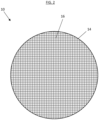
- the conductive pathways 16 are arranged in a grid pattern.
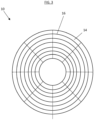
- the conductive pathways 16 are arranged in a ring and spoke pattern, that is interconnected between the circular portions of the conductive pathways 16, or alternatively in another pattern such as a spoked spiral pattern.
- the conductive pathways illustrated in FIG. 2 and 3 are merely exemplary, and that other arrangements of conductive pathways 16 may be utilized to achieve a desired level of EMI shielding of the cover 10.
- the cover 10 is a layered structure, having multiple cover layers 24 to form the cap 10.
- the cover 10 may include two cover layers 24, each cover layer 24 including a plastic material layer 14 having electrically conductive ink 18 applied thereto to define one or more conductive pathways 16.
- the cover layers 24 may be stacked such that a first electrically conductive ink 18a of a first cover layer 24a does not contact a second electrically conductive ink 18b of an adjacent second cover layer 24b.
- One of the plastic material layers 14, such as a first plastic material layer 14a of the first cover layer 24a may be positioned between the first electrically conductive ink 18a and the second electrically conductive ink 18b to keep the first electrically conductive ink 18a separated from the second electrically conductive ink 18b.
- the plastic material layer 14 is continuous covering the pathway portions 20 and the spacing, while in other embodiments the plastic material layer 14 is localized and present only in areas where the first electrically conductive ink 18a pathway portions 20a overlap the second electrically conductive ink 18b pathway portions 20b.
- a light 26 for example, a light-emitting diode (LED), is incorporated or embedded into the cover 10.
- the light 26 may be disposed between the first cover layer 24a and the second cover layer 24b. As shown, the light 26 may be connected to the first electrically conductive ink 18a, which is connected to a power source 28 defining a circuit for operation of the light 26. As shown, the second electrically conductive ink 18b may be connected to electrical ground 30. In the embodiment shown in FIG. 4 , while the first electrically conductive ink 18a provides power to the light 26, the second electrically conductive ink 18b provides the desired EMI shielding. It should be appreciated that in certain instances the light 26 may be disposed on the exterior of the cover 10 (as opposed to being disposed between the cover layers 24a and 24b), and receive power from the first electrically conductive ink 18a. For example, the light 26 may be disposed on the external surface of the first electrically conductive ink 18a, instead of being disposed in the plastic layer between the first electrically conductive ink 18a and the second electrically conductive ink 18b.
- the cover layers 24 are formed in flat sheets, with the electrically conductive ink 18 applied to the flat plastic material sheet 14.
- Example methods of application of the conductive ink may include extrusion, screen printing, pad printing, gravure application, or the like.
- the cover layers 24 may then be formed to their desired shape to define the cover 10.
- An exemplary method of forming the cover 10 is illustrated in FIG. 5 .
- the plastic material sheet 14 is formed, and in step 102 the electrically conductive ink 18 is applied to the plastic material sheet 14 to define the electrically conductive pathways 16 and the cover layers 24.
- the cover layers 24 are stacked, which may include embedding the light 26 between the cover layers 24.
- the light 26 may be disposed on the exterior of the cover 10 (as opposed to between the cover layers 24a and 24b), in certain instances.
- the cover layers 24 are stacked the cover layers 24 are fused together and formed to a selected shape to define the cover 10 at step 106 by, for example, injection molding or thermoforming to form the structural cover 10.
Landscapes
- Engineering & Computer Science (AREA)
- Chemical & Material Sciences (AREA)
- Physics & Mathematics (AREA)
- Life Sciences & Earth Sciences (AREA)
- Health & Medical Sciences (AREA)
- Microelectronics & Electronic Packaging (AREA)
- Electromagnetism (AREA)
- Combustion & Propulsion (AREA)
- Food Science & Technology (AREA)
- Medicinal Chemistry (AREA)
- Analytical Chemistry (AREA)
- Biochemistry (AREA)
- General Health & Medical Sciences (AREA)
- General Physics & Mathematics (AREA)
- Immunology (AREA)
- Pathology (AREA)
- Textile Engineering (AREA)
- Shielding Devices Or Components To Electric Or Magnetic Fields (AREA)
Abstract
Description
- Exemplary embodiments pertain to the art of gas detectors, and more specifically, to electromagnetic interference (EMI) shielding of gas detectors.
- A product requirement for a new gas detector states that the detector must have light indicators while a second requirement is to have EMI protection for the circuitry of the gas detector to prevent disruption of the operation of the gas detector circuitry. Current gas detectors typically do not include such protection. Meeting each of these requirements may present issues in the sense that EMI shields require conductive material, which are typically not transparent, while light indicators require transparent material or openings of no material to allow light transmission.
- Viewed from a first aspect, there is provided an electromagnetic interference (EMI) cover for a gas detector including one or more electrical components. The EMI cover includes one or more cover layers, each cover layer including a plastic material layer and one or more layers of conductive or dielectric ink applied to the plastic material layer defining one or more conductive pathways. The one or more conductive pathways are positioned in a pattern to provide electromagnetic interference (EMI) shielding to the one or more electrical component.
- The one or more conductive pathways may be arranged in one of a grid pattern, a spoke and spiral pattern, or a spoke and wheel pattern.
- The plastic material layer may be transparent or translucent.
- The one or more cover layers may include a first cover layer and a second cover layer arranged in a stack.
- A first plastic material layer of the first cover layer may be positioned between a first electrically conductive ink layer of the first cover layer and a second electrically conductive ink layer of the second cover layer.
- The first electrically conductive ink layer may be arranged in a first pattern and the second electrically conductive ink layer may be arranged in a second pattern different from the first pattern.
- At least one light source may be embedded in the stack or positioned on an exterior surface of the stack.
- The light source may be a light emitting diode.
- The first electrically conductive ink layer may be operably connected to the light source to power the light source, and the second electrically conductive ink layer may be connected to electrical ground.
- Viewed from a second aspect, there is provided a method of forming an electromagnetic interference (EMI) cover for a gas detector including one or more electrical component includes forming a plastic material layer, applying an electrically conductive ink layer to the plastic material layer forming one or more electrically conductive pathways, thereby defining one or more cover layers. The one or more cover layers are formed into a desired cover shape. The one or more conductive pathways are located in a pattern to provide electromagnetic interference (EMI) shielding to the one or more electrical component.
- The electrically conductive ink may be applied in one of a grid pattern, a spoke and spiral pattern, or a wheel and spoke pattern.
- Two or more cover layers may be formed, and the two or more cover layers may be arranged in a stack.
- The stack may be arranged such that a first plastic material layer of a first cover layer is located between a first electrically conductive ink layer of the first cover layer and a second electrically conductive ink layer of a second cover layer.
- The first electrically conductive ink layer may be arranged in a first pattern and the second electrically conductive ink layer may be arranged in a second pattern different from the first pattern.
- At least one light source may be embedded or positioned in the stack or on an exterior surface of the stack.
- The light source may be a light emitting diode.
- The first electrically conductive ink layer may be operably connected to the light source to power the light source, and the second electrically conductive ink layer may be connected to electrical ground.
- The one or more cover layers may be formed to the desired cover shape via an injection molding process.
- Certain exemplary embodiments will now be described in greater detail by way of example only and with reference to the accompanying drawings in which:
-
FIG. 1 is a perspective view of a cover with EMI shielding; -
FIG. 2 is a plane view of an electrically conductive pathway arrangement in a cover; -
FIG. 3 is a plane view of another electrically conductive pathway arrangement in a cover; -
FIG. 4 is a cross-sectional view of a cover; and -
FIG. 5 is a flow diagram illustrating a method of forming a cover with EMI shielding. - A detailed description of one or more embodiments of the disclosed apparatus and method are presented herein by way of exemplification and not limitation with reference to the Figures.
-
FIG. 1 is a perspective view of acover 10 with electromagnetic interference (EMI) shielding. Although described herein that thecover 10 may be incorporated as a component of agas detector 12, it should be appreciated that the application of the EMI shielding process described herein within any product is within the scope of the current disclosure. As shown inFIG. 1 , thecover 10 may be positioned over the exterior of thegas detector 12 such that thecomponents 12 behind the cover 10 (e.g., the gas detector circuitry) are protected from electromagnetic interference. As will be described below, the features of thecover 10 are provided to produce the EMI shielding for thecomponents 12. - The
cover 10 may be formed from one or moreplastic material layers 14, which in some embodiments are formed from a transparent or translucent plastic material. One or more electricallyconductive pathways 16 are embedded in thecover 10. Theconductive pathways 16 are formed by, for example, electricallyconductive ink 18 applied to one or more of theplastic material layers 14. Theconductive pathways 16 may be formed into a pattern, for example, a grid pattern or the like. The pattern includes a plurality ofpathway portions 20 having a selectedspacing 22 betweenadjacent pathway portions 20 to provide a selected coverage of theconductive pathways 16 in thecover 10, thus providing a desired level of EMI shielding in thecover 10. In at least one embodiment, thespacing 22 betweenadjacent pathway portions 20 is configured to provide shielding of up to a 6Ghz frequency with amaximum spacing 22 of five (5) millimeters. In other embodiments,other spacing 22 may be used depending on the desired shielding, withsmaller spacing 22 utilized to provide greater maximum shielding frequency. - Referring now to
FIG. 2 , in some embodiments theconductive pathways 16 are arranged in a grid pattern. In other embodiments, such as shown inFIG. 3 , theconductive pathways 16 are arranged in a ring and spoke pattern, that is interconnected between the circular portions of theconductive pathways 16, or alternatively in another pattern such as a spoked spiral pattern. One skilled in the art will readily appreciate that the conductive pathways illustrated inFIG. 2 and3 are merely exemplary, and that other arrangements ofconductive pathways 16 may be utilized to achieve a desired level of EMI shielding of thecover 10. - Referring now to
FIG. 4 , illustrated is a cross-sectional view of an embodiment of acover 10. Thecover 10 is a layered structure, having multiple cover layers 24 to form thecap 10. For example, thecover 10 may include two cover layers 24, each cover layer 24 including aplastic material layer 14 having electricallyconductive ink 18 applied thereto to define one or moreconductive pathways 16. The cover layers 24 may be stacked such that a first electricallyconductive ink 18a of afirst cover layer 24a does not contact a second electricallyconductive ink 18b of an adjacentsecond cover layer 24b. One of theplastic material layers 14, such as a firstplastic material layer 14a of thefirst cover layer 24a may be positioned between the first electricallyconductive ink 18a and the second electricallyconductive ink 18b to keep the first electricallyconductive ink 18a separated from the second electricallyconductive ink 18b. In some embodiments, theplastic material layer 14 is continuous covering thepathway portions 20 and the spacing, while in other embodiments theplastic material layer 14 is localized and present only in areas where the first electricallyconductive ink 18a pathway portions 20a overlap the second electricallyconductive ink 18b pathway portions 20b. In some embodiments, alight 26, for example, a light-emitting diode (LED), is incorporated or embedded into thecover 10. For example, thelight 26 may be disposed between thefirst cover layer 24a and thesecond cover layer 24b. As shown, thelight 26 may be connected to the first electricallyconductive ink 18a, which is connected to apower source 28 defining a circuit for operation of thelight 26. As shown, the second electricallyconductive ink 18b may be connected toelectrical ground 30. In the embodiment shown inFIG. 4 , while the first electricallyconductive ink 18a provides power to thelight 26, the second electricallyconductive ink 18b provides the desired EMI shielding. It should be appreciated that in certain instances thelight 26 may be disposed on the exterior of the cover 10 (as opposed to being disposed between thecover layers conductive ink 18a. For example, thelight 26 may be disposed on the external surface of the first electricallyconductive ink 18a, instead of being disposed in the plastic layer between the first electricallyconductive ink 18a and the second electricallyconductive ink 18b. - In some embodiments, the cover layers 24 are formed in flat sheets, with the electrically
conductive ink 18 applied to the flatplastic material sheet 14. Example methods of application of the conductive ink may include extrusion, screen printing, pad printing, gravure application, or the like. The cover layers 24 may then be formed to their desired shape to define thecover 10. An exemplary method of forming thecover 10 is illustrated inFIG. 5 . Instep 100, theplastic material sheet 14 is formed, and instep 102 the electricallyconductive ink 18 is applied to theplastic material sheet 14 to define the electricallyconductive pathways 16 and the cover layers 24. Atstep 104 the cover layers 24 are stacked, which may include embedding the light 26 between the cover layers 24. As described above, the light 26 may be disposed on the exterior of the cover 10 (as opposed to between the cover layers 24a and 24b), in certain instances. Once the cover layers 24 are stacked the cover layers 24 are fused together and formed to a selected shape to define thecover 10 atstep 106 by, for example, injection molding or thermoforming to form thestructural cover 10. - The term "about" is intended to include the degree of error associated with measurement of the particular quantity based upon the equipment available at the time of filing the application.
- The terminology used herein is for the purpose of describing particular embodiments only and is not intended to be limiting of the present disclosure. As used herein, the singular forms "a", "an" and "the" are intended to include the plural forms as well, unless the context clearly indicates otherwise. It will be further understood that the terms "comprises" and/or "comprising," when used in this specification, specify the presence of stated features, integers, steps, operations, elements, and/or components, but do not preclude the presence or addition of one or more other features, integers, steps, operations, element components, and/or groups thereof.
- While the present disclosure has been described with reference to an exemplary embodiment or embodiments, it will be understood by those skilled in the art that various changes may be made and equivalents may be substituted for elements thereof without departing from the scope of the present invention as set out in the appended claims. In addition, many modifications may be made to adapt a particular situation or material to the teachings of the present disclosure without departing from the essential scope of the invention. Therefore, it is intended that the present invention not be limited to the particular embodiment disclosed as the best mode contemplated for carrying out this present disclosure, but that the present invention will include all embodiments falling within the scope of the claims.
Claims (15)
- An electromagnetic interference (EMI) cover (10) for a gas detector (12) comprising one or more electrical component, the EMI cover comprising:one or more cover layers (24), each cover layer including:a plastic material layer (14); andone or more layers of conductive or dielectric ink (18) applied to the plastic material layer (14) defining one or more conductive pathways (16);wherein the one or more conductive pathways (16) are disposed in a pattern to provide electromagnetic interference (EMI) shielding to the one or more electrical component (12).
- The EMI cover of claim 1, wherein the one or more conductive pathways (16) are arranged in one of a grid pattern, a spoke and spiral pattern, or a spoke and wheel pattern.
- The EMI cover of claim 1 or 2, wherein the plastic material layer (14) is transparent or translucent.
- The EMI cover of claim 1, 2 or 3, wherein the one or more cover layers (24) comprise a first cover layer (24a) and a second cover layer (24b) arranged in a stack.
- The EMI cover of claim 4, wherein a first plastic material layer (14a) of the first cover layer (24a) is disposed between a first electrically conductive ink layer (18a) of the first cover layer (24a) and a second electrically conductive ink layer (18b) of the second cover layer (24b).
- The EMI cover of claim 5, wherein the first electrically conductive ink (18a) layer is arranged in a first pattern and the second electrically conductive ink (18b) layer is arranged in a second pattern different from the first pattern.
- The EMI cover of claim 5 or 6, further comprising at least one light source (26) embedded in the stack or disposed on an exterior surface of the stack, optionally wherein the light source (26) is a light emitting diode.
- The EMI cover of claim 7, wherein:the first electrically conductive ink layer (18a) is operably connected to the light source (26) to power the light source; andthe second electrically conductive ink layer (18b) is connected to electrical ground (30).
- A method of forming an electromagnetic interference (EMI) cover (10) for a gas detector (12) comprising one or more electrical component, the method comprising:forming (100) a plastic material layer (14);applying (102) an electrically conductive ink layer (18) to the plastic material layer (14) forming one or more electrically conductive pathways (16), thereby defining one or more cover layers (24); andforming (106) the one or more cover layers (24) into a desired cover shape;wherein the one or more conductive pathways (16) are disposed in a pattern to provide electromagnetic interference (EMI) shielding to the one or more electrical component.
- The method of claim 9, further comprising applying the electrically conductive ink (18) in one of a grid pattern, a spoke and spiral pattern, or a wheel and spoke pattern.
- The method of claim 9 or 10, further comprising:forming two or more cover layers(24); andarranging (104) the two or more cover layers (24) in a stack.
- The method of claim 11, further comprising arranging the stack such that a first plastic material layer of a first cover layer (24a) is disposed between a first electrically conductive ink layer (18a) of the first cover layer (24a) and a second electrically conductive ink layer (18b) of a second cover layer (24b), optionally wherein the first electrically conductive ink (18a) layer is arranged in a first pattern and the second electrically conductive ink (18b) layer is arranged in a second pattern different from the first pattern.
- The method of claim 12, further comprising embedding or disposing at least one light source (26) in the stack or on an exterior surface of the stack, optionally wherein the light source (26) is a light emitting diode.
- The method of claim 13, further comprising:operably connecting the first electrically conductive ink layer (18a) to the light source (26) to power the light source; andconnecting the second electrically conductive ink layer (18b) to electrical ground (30).
- The method of any of claims 9 to 14, wherein the one or more cover layers (24) are formed to the desired cover shape via an injection molding process.
Applications Claiming Priority (1)
| Application Number | Priority Date | Filing Date | Title |
|---|---|---|---|
| US202263338106P | 2022-05-04 | 2022-05-04 |
Publications (2)
| Publication Number | Publication Date |
|---|---|
| EP4273544A1 true EP4273544A1 (en) | 2023-11-08 |
| EP4273544B1 EP4273544B1 (en) | 2025-08-13 |
Family
ID=86329000
Family Applications (1)
| Application Number | Title | Priority Date | Filing Date |
|---|---|---|---|
| EP23171318.1A Active EP4273544B1 (en) | 2022-05-04 | 2023-05-03 | Electromagnetic interference shielding of gas detector |
Country Status (2)
| Country | Link |
|---|---|
| US (1) | US12550305B2 (en) |
| EP (1) | EP4273544B1 (en) |
Citations (2)
| Publication number | Priority date | Publication date | Assignee | Title |
|---|---|---|---|---|
| US20160113161A1 (en) * | 2014-10-17 | 2016-04-21 | Laird Technologies, Inc. | Electromagnetic interference (emi) shields including see-through portions |
| KR20210049093A (en) * | 2018-08-27 | 2021-05-04 | 택토텍 오와이 | Multi-layered structures with built-in sensing and related manufacturing methods |
Family Cites Families (1)
| Publication number | Priority date | Publication date | Assignee | Title |
|---|---|---|---|---|
| JP2010541285A (en) * | 2007-10-02 | 2010-12-24 | パーカー.ハニフィン.コーポレイション | Nano ink for providing EMI shielding to windows |
-
2023
- 2023-05-03 EP EP23171318.1A patent/EP4273544B1/en active Active
- 2023-05-03 US US18/311,311 patent/US12550305B2/en active Active
Patent Citations (2)
| Publication number | Priority date | Publication date | Assignee | Title |
|---|---|---|---|---|
| US20160113161A1 (en) * | 2014-10-17 | 2016-04-21 | Laird Technologies, Inc. | Electromagnetic interference (emi) shields including see-through portions |
| KR20210049093A (en) * | 2018-08-27 | 2021-05-04 | 택토텍 오와이 | Multi-layered structures with built-in sensing and related manufacturing methods |
Also Published As
| Publication number | Publication date |
|---|---|
| EP4273544B1 (en) | 2025-08-13 |
| US20230363127A1 (en) | 2023-11-09 |
| US12550305B2 (en) | 2026-02-10 |
Similar Documents
| Publication | Publication Date | Title |
|---|---|---|
| US11285645B2 (en) | Method for manufacturing an electronic assembly and an electronic assembly | |
| JP5957132B1 (en) | Touch panel | |
| KR101657951B1 (en) | Conductive sheet and manufacturing method for same | |
| CN103369938B (en) | Comb structure shielding layer and its wireless charging transmitter | |
| EP2579293B1 (en) | Ion mobility tube | |
| US20190019436A1 (en) | Display body device and display apparatus | |
| JP2015526862A (en) | ELECTRO-OPTICAL COMPONENT AND METHOD FOR MANUFACTURING THE SAME | |
| CN101014237A (en) | Permeable conductive shield having a laminated structure | |
| KR101893839B1 (en) | Wiring board | |
| KR20120029433A (en) | Electronic device having an inductive receiver coil with ultra-thin shielding layer and method | |
| CN104094431A (en) | Oled device and manufacture thereof | |
| EP4273544B1 (en) | Electromagnetic interference shielding of gas detector | |
| US7898821B2 (en) | Apparatus and arrangement for shielding a light emitting diode against electrostatic discharge | |
| US20120247826A1 (en) | Circuit board having circumferential shielding layer | |
| KR20170063593A (en) | Organic el panel and method for producing same | |
| CN107770944A (en) | Circuit board and its manufacture method with electro-magnetic screen function | |
| EP3871274B1 (en) | Led package | |
| US20160174419A1 (en) | Shielded RF Transmission Lines in Low Temperature Co-fired Ceramic Constructs and Method of Making Same | |
| US20160212859A1 (en) | Printing electronic circuitry | |
| US12035449B2 (en) | Keypad overlay with electrostatic discharge dissipation | |
| TW200511886A (en) | Method for manufacturing an organic electronic device and organic electronic device | |
| CN103716994B (en) | The preparation method of a kind of printed circuit board and printed circuit board thereof | |
| US20160351307A1 (en) | Method for manufacturing thin film chip resistor device | |
| JP2001196638A (en) | Light emitting diode electrostatic protection device | |
| EP4152131A1 (en) | Layered device for pressure treatment and method |
Legal Events
| Date | Code | Title | Description |
|---|---|---|---|
| PUAI | Public reference made under article 153(3) epc to a published international application that has entered the european phase |
Free format text: ORIGINAL CODE: 0009012 |
|
| STAA | Information on the status of an ep patent application or granted ep patent |
Free format text: STATUS: THE APPLICATION HAS BEEN PUBLISHED |
|
| AK | Designated contracting states |
Kind code of ref document: A1 Designated state(s): AL AT BE BG CH CY CZ DE DK EE ES FI FR GB GR HR HU IE IS IT LI LT LU LV MC ME MK MT NL NO PL PT RO RS SE SI SK SM TR |
|
| STAA | Information on the status of an ep patent application or granted ep patent |
Free format text: STATUS: REQUEST FOR EXAMINATION WAS MADE |
|
| 17P | Request for examination filed |
Effective date: 20240501 |
|
| RBV | Designated contracting states (corrected) |
Designated state(s): AL AT BE BG CH CY CZ DE DK EE ES FI FR GB GR HR HU IE IS IT LI LT LU LV MC ME MK MT NL NO PL PT RO RS SE SI SK SM TR |
|
| GRAP | Despatch of communication of intention to grant a patent |
Free format text: ORIGINAL CODE: EPIDOSNIGR1 |
|
| STAA | Information on the status of an ep patent application or granted ep patent |
Free format text: STATUS: GRANT OF PATENT IS INTENDED |
|
| RIC1 | Information provided on ipc code assigned before grant |
Ipc: G01N 33/00 20060101AFI20250417BHEP |
|
| INTG | Intention to grant announced |
Effective date: 20250506 |
|
| GRAS | Grant fee paid |
Free format text: ORIGINAL CODE: EPIDOSNIGR3 |
|
| GRAA | (expected) grant |
Free format text: ORIGINAL CODE: 0009210 |
|
| STAA | Information on the status of an ep patent application or granted ep patent |
Free format text: STATUS: THE PATENT HAS BEEN GRANTED |
|
| AK | Designated contracting states |
Kind code of ref document: B1 Designated state(s): AL AT BE BG CH CY CZ DE DK EE ES FI FR GB GR HR HU IE IS IT LI LT LU LV MC ME MK MT NL NO PL PT RO RS SE SI SK SM TR |
|
| REG | Reference to a national code |
Ref country code: GB Ref legal event code: FG4D |
|
| REG | Reference to a national code |
Ref country code: CH Ref legal event code: EP |
|
| REG | Reference to a national code |
Ref country code: DE Ref legal event code: R096 Ref document number: 602023005609 Country of ref document: DE |
|
| REG | Reference to a national code |
Ref country code: IE Ref legal event code: FG4D |
|
| REG | Reference to a national code |
Ref country code: NL Ref legal event code: MP Effective date: 20250813 |
|
| PG25 | Lapsed in a contracting state [announced via postgrant information from national office to epo] |
Ref country code: IS Free format text: LAPSE BECAUSE OF FAILURE TO SUBMIT A TRANSLATION OF THE DESCRIPTION OR TO PAY THE FEE WITHIN THE PRESCRIBED TIME-LIMIT Effective date: 20251213 |
|
| REG | Reference to a national code |
Ref country code: LT Ref legal event code: MG9D |
|
| PG25 | Lapsed in a contracting state [announced via postgrant information from national office to epo] |
Ref country code: PT Free format text: LAPSE BECAUSE OF FAILURE TO SUBMIT A TRANSLATION OF THE DESCRIPTION OR TO PAY THE FEE WITHIN THE PRESCRIBED TIME-LIMIT Effective date: 20251215 |
|
| PG25 | Lapsed in a contracting state [announced via postgrant information from national office to epo] |
Ref country code: FI Free format text: LAPSE BECAUSE OF FAILURE TO SUBMIT A TRANSLATION OF THE DESCRIPTION OR TO PAY THE FEE WITHIN THE PRESCRIBED TIME-LIMIT Effective date: 20250813 |
|
| PG25 | Lapsed in a contracting state [announced via postgrant information from national office to epo] |
Ref country code: HR Free format text: LAPSE BECAUSE OF FAILURE TO SUBMIT A TRANSLATION OF THE DESCRIPTION OR TO PAY THE FEE WITHIN THE PRESCRIBED TIME-LIMIT Effective date: 20250813 Ref country code: NL Free format text: LAPSE BECAUSE OF FAILURE TO SUBMIT A TRANSLATION OF THE DESCRIPTION OR TO PAY THE FEE WITHIN THE PRESCRIBED TIME-LIMIT Effective date: 20250813 |
|
| PG25 | Lapsed in a contracting state [announced via postgrant information from national office to epo] |
Ref country code: GR Free format text: LAPSE BECAUSE OF FAILURE TO SUBMIT A TRANSLATION OF THE DESCRIPTION OR TO PAY THE FEE WITHIN THE PRESCRIBED TIME-LIMIT Effective date: 20251114 |
|
| PG25 | Lapsed in a contracting state [announced via postgrant information from national office to epo] |
Ref country code: SE Free format text: LAPSE BECAUSE OF FAILURE TO SUBMIT A TRANSLATION OF THE DESCRIPTION OR TO PAY THE FEE WITHIN THE PRESCRIBED TIME-LIMIT Effective date: 20250813 |
|
| PG25 | Lapsed in a contracting state [announced via postgrant information from national office to epo] |
Ref country code: LV Free format text: LAPSE BECAUSE OF FAILURE TO SUBMIT A TRANSLATION OF THE DESCRIPTION OR TO PAY THE FEE WITHIN THE PRESCRIBED TIME-LIMIT Effective date: 20250813 |
|
| PG25 | Lapsed in a contracting state [announced via postgrant information from national office to epo] |
Ref country code: BG Free format text: LAPSE BECAUSE OF FAILURE TO SUBMIT A TRANSLATION OF THE DESCRIPTION OR TO PAY THE FEE WITHIN THE PRESCRIBED TIME-LIMIT Effective date: 20250813 Ref country code: PL Free format text: LAPSE BECAUSE OF FAILURE TO SUBMIT A TRANSLATION OF THE DESCRIPTION OR TO PAY THE FEE WITHIN THE PRESCRIBED TIME-LIMIT Effective date: 20250813 |
|
| PG25 | Lapsed in a contracting state [announced via postgrant information from national office to epo] |
Ref country code: RS Free format text: LAPSE BECAUSE OF FAILURE TO SUBMIT A TRANSLATION OF THE DESCRIPTION OR TO PAY THE FEE WITHIN THE PRESCRIBED TIME-LIMIT Effective date: 20251113 |
|
| PG25 | Lapsed in a contracting state [announced via postgrant information from national office to epo] |
Ref country code: ES Free format text: LAPSE BECAUSE OF FAILURE TO SUBMIT A TRANSLATION OF THE DESCRIPTION OR TO PAY THE FEE WITHIN THE PRESCRIBED TIME-LIMIT Effective date: 20250813 |
|
| REG | Reference to a national code |
Ref country code: DE Ref legal event code: R081 Ref document number: 602023005609 Country of ref document: DE Owner name: DETECTOR ELECTRONICS BUYER US, LLC, BLOOMINGTO, US Free format text: FORMER OWNER: CARRIER CORPORATION, PALM BEACH GARDENS, FL, US |
|
| REG | Reference to a national code |
Ref country code: AT Ref legal event code: MK05 Ref document number: 1825170 Country of ref document: AT Kind code of ref document: T Effective date: 20250813 |
|
| REG | Reference to a national code |
Ref country code: CH Ref legal event code: W10 Free format text: ST27 STATUS EVENT CODE: U-0-0-W10-W00 (AS PROVIDED BY THE NATIONAL OFFICE) Effective date: 20260225 |
|
| RAP2 | Party data changed (patent owner data changed or rights of a patent transferred) |
Owner name: DETECTOR ELECTRONICS BUYER US, LLC |
|
| REG | Reference to a national code |
Ref country code: GB Ref legal event code: 732E Free format text: REGISTERED BETWEEN 20260305 AND 20260311 |
|
| PG25 | Lapsed in a contracting state [announced via postgrant information from national office to epo] |
Ref country code: SM Free format text: LAPSE BECAUSE OF FAILURE TO SUBMIT A TRANSLATION OF THE DESCRIPTION OR TO PAY THE FEE WITHIN THE PRESCRIBED TIME-LIMIT Effective date: 20250813 |
|
| PG25 | Lapsed in a contracting state [announced via postgrant information from national office to epo] |
Ref country code: DK Free format text: LAPSE BECAUSE OF FAILURE TO SUBMIT A TRANSLATION OF THE DESCRIPTION OR TO PAY THE FEE WITHIN THE PRESCRIBED TIME-LIMIT Effective date: 20250813 |
|
| PG25 | Lapsed in a contracting state [announced via postgrant information from national office to epo] |
Ref country code: AT Free format text: LAPSE BECAUSE OF FAILURE TO SUBMIT A TRANSLATION OF THE DESCRIPTION OR TO PAY THE FEE WITHIN THE PRESCRIBED TIME-LIMIT Effective date: 20250813 |
|
| PG25 | Lapsed in a contracting state [announced via postgrant information from national office to epo] |
Ref country code: IT Free format text: LAPSE BECAUSE OF FAILURE TO SUBMIT A TRANSLATION OF THE DESCRIPTION OR TO PAY THE FEE WITHIN THE PRESCRIBED TIME-LIMIT Effective date: 20250813 |
|
| PG25 | Lapsed in a contracting state [announced via postgrant information from national office to epo] |
Ref country code: CZ Free format text: LAPSE BECAUSE OF FAILURE TO SUBMIT A TRANSLATION OF THE DESCRIPTION OR TO PAY THE FEE WITHIN THE PRESCRIBED TIME-LIMIT Effective date: 20250813 |
|
| PG25 | Lapsed in a contracting state [announced via postgrant information from national office to epo] |
Ref country code: EE Free format text: LAPSE BECAUSE OF FAILURE TO SUBMIT A TRANSLATION OF THE DESCRIPTION OR TO PAY THE FEE WITHIN THE PRESCRIBED TIME-LIMIT Effective date: 20250813 Ref country code: SK Free format text: LAPSE BECAUSE OF FAILURE TO SUBMIT A TRANSLATION OF THE DESCRIPTION OR TO PAY THE FEE WITHIN THE PRESCRIBED TIME-LIMIT Effective date: 20250813 |