EP4273507A1 - Scanning element and inductive position measuring device with the same - Google Patents
Scanning element and inductive position measuring device with the same Download PDFInfo
- Publication number
- EP4273507A1 EP4273507A1 EP22171709.3A EP22171709A EP4273507A1 EP 4273507 A1 EP4273507 A1 EP 4273507A1 EP 22171709 A EP22171709 A EP 22171709A EP 4273507 A1 EP4273507 A1 EP 4273507A1
- Authority
- EP
- European Patent Office
- Prior art keywords
- conductor
- conductor track
- track
- receiver
- scanning element
- Prior art date
- Legal status (The legal status is an assumption and is not a legal conclusion. Google has not performed a legal analysis and makes no representation as to the accuracy of the status listed.)
- Granted
Links
- 230000001939 inductive effect Effects 0.000 title claims description 12
- 239000004020 conductor Substances 0.000 claims abstract description 227
- 230000005284 excitation Effects 0.000 claims description 28
- 239000000758 substrate Substances 0.000 claims description 8
- 239000007769 metal material Substances 0.000 claims description 3
- 238000011156 evaluation Methods 0.000 description 5
- 238000005259 measurement Methods 0.000 description 5
- 230000001419 dependent effect Effects 0.000 description 3
- 238000006073 displacement reaction Methods 0.000 description 2
- 230000005672 electromagnetic field Effects 0.000 description 2
- 239000002184 metal Substances 0.000 description 2
- 229910052751 metal Inorganic materials 0.000 description 2
- 230000000737 periodic effect Effects 0.000 description 2
- 229920001721 polyimide Polymers 0.000 description 2
- RYGMFSIKBFXOCR-UHFFFAOYSA-N Copper Chemical compound [Cu] RYGMFSIKBFXOCR-UHFFFAOYSA-N 0.000 description 1
- 239000004642 Polyimide Substances 0.000 description 1
- 230000015572 biosynthetic process Effects 0.000 description 1
- 229910052802 copper Inorganic materials 0.000 description 1
- 239000010949 copper Substances 0.000 description 1
- 230000000694 effects Effects 0.000 description 1
- 239000003822 epoxy resin Substances 0.000 description 1
- 239000011888 foil Substances 0.000 description 1
- 230000006698 induction Effects 0.000 description 1
- 239000000696 magnetic material Substances 0.000 description 1
- 239000000463 material Substances 0.000 description 1
- 229920000647 polyepoxide Polymers 0.000 description 1
- 230000002787 reinforcement Effects 0.000 description 1
Images


Classifications
-
- G—PHYSICS
- G01—MEASURING; TESTING
- G01B—MEASURING LENGTH, THICKNESS OR SIMILAR LINEAR DIMENSIONS; MEASURING ANGLES; MEASURING AREAS; MEASURING IRREGULARITIES OF SURFACES OR CONTOURS
- G01B7/00—Measuring arrangements characterised by the use of electric or magnetic techniques
- G01B7/003—Measuring arrangements characterised by the use of electric or magnetic techniques for measuring position, not involving coordinate determination
-
- G—PHYSICS
- G01—MEASURING; TESTING
- G01D—MEASURING NOT SPECIALLY ADAPTED FOR A SPECIFIC VARIABLE; ARRANGEMENTS FOR MEASURING TWO OR MORE VARIABLES NOT COVERED IN A SINGLE OTHER SUBCLASS; TARIFF METERING APPARATUS; MEASURING OR TESTING NOT OTHERWISE PROVIDED FOR
- G01D5/00—Mechanical means for transferring the output of a sensing member; Means for converting the output of a sensing member to another variable where the form or nature of the sensing member does not constrain the means for converting; Transducers not specially adapted for a specific variable
- G01D5/12—Mechanical means for transferring the output of a sensing member; Means for converting the output of a sensing member to another variable where the form or nature of the sensing member does not constrain the means for converting; Transducers not specially adapted for a specific variable using electric or magnetic means
- G01D5/14—Mechanical means for transferring the output of a sensing member; Means for converting the output of a sensing member to another variable where the form or nature of the sensing member does not constrain the means for converting; Transducers not specially adapted for a specific variable using electric or magnetic means influencing the magnitude of a current or voltage
- G01D5/20—Mechanical means for transferring the output of a sensing member; Means for converting the output of a sensing member to another variable where the form or nature of the sensing member does not constrain the means for converting; Transducers not specially adapted for a specific variable using electric or magnetic means influencing the magnitude of a current or voltage by varying inductance, e.g. by a movable armature
- G01D5/204—Mechanical means for transferring the output of a sensing member; Means for converting the output of a sensing member to another variable where the form or nature of the sensing member does not constrain the means for converting; Transducers not specially adapted for a specific variable using electric or magnetic means influencing the magnitude of a current or voltage by varying inductance, e.g. by a movable armature by influencing the mutual induction between two or more coils
- G01D5/2053—Mechanical means for transferring the output of a sensing member; Means for converting the output of a sensing member to another variable where the form or nature of the sensing member does not constrain the means for converting; Transducers not specially adapted for a specific variable using electric or magnetic means influencing the magnitude of a current or voltage by varying inductance, e.g. by a movable armature by influencing the mutual induction between two or more coils by a movable non-ferromagnetic conductive element
-
- G—PHYSICS
- G01—MEASURING; TESTING
- G01B—MEASURING LENGTH, THICKNESS OR SIMILAR LINEAR DIMENSIONS; MEASURING ANGLES; MEASURING AREAS; MEASURING IRREGULARITIES OF SURFACES OR CONTOURS
- G01B7/00—Measuring arrangements characterised by the use of electric or magnetic techniques
- G01B7/30—Measuring arrangements characterised by the use of electric or magnetic techniques for measuring angles or tapers; for testing the alignment of axes
-
- G—PHYSICS
- G01—MEASURING; TESTING
- G01D—MEASURING NOT SPECIALLY ADAPTED FOR A SPECIFIC VARIABLE; ARRANGEMENTS FOR MEASURING TWO OR MORE VARIABLES NOT COVERED IN A SINGLE OTHER SUBCLASS; TARIFF METERING APPARATUS; MEASURING OR TESTING NOT OTHERWISE PROVIDED FOR
- G01D5/00—Mechanical means for transferring the output of a sensing member; Means for converting the output of a sensing member to another variable where the form or nature of the sensing member does not constrain the means for converting; Transducers not specially adapted for a specific variable
- G01D5/12—Mechanical means for transferring the output of a sensing member; Means for converting the output of a sensing member to another variable where the form or nature of the sensing member does not constrain the means for converting; Transducers not specially adapted for a specific variable using electric or magnetic means
- G01D5/14—Mechanical means for transferring the output of a sensing member; Means for converting the output of a sensing member to another variable where the form or nature of the sensing member does not constrain the means for converting; Transducers not specially adapted for a specific variable using electric or magnetic means influencing the magnitude of a current or voltage
- G01D5/20—Mechanical means for transferring the output of a sensing member; Means for converting the output of a sensing member to another variable where the form or nature of the sensing member does not constrain the means for converting; Transducers not specially adapted for a specific variable using electric or magnetic means influencing the magnitude of a current or voltage by varying inductance, e.g. by a movable armature
- G01D5/204—Mechanical means for transferring the output of a sensing member; Means for converting the output of a sensing member to another variable where the form or nature of the sensing member does not constrain the means for converting; Transducers not specially adapted for a specific variable using electric or magnetic means influencing the magnitude of a current or voltage by varying inductance, e.g. by a movable armature by influencing the mutual induction between two or more coils
Definitions
- the invention relates to a scanning element for an inductive position measuring device according to claim 1 for determining the position of the scanning element relative to a scale element and to a position measuring device with such a scanning element.
- Inductive position measuring devices are used, for example, as angle measuring devices to determine the angular position of machine parts that can rotate relative to one another.
- exciter tracks and receiver tracks are often applied in the form of conductor tracks on a common, usually multi-layer circuit board, which is firmly connected, for example, to a stator of an angle measuring device.
- this circuit board there is a scale element on which graduation structures are applied and which is connected in a rotationally fixed manner to the rotor of the angle measuring device. If a time-changing electrical excitation current is applied to the excitation conductor tracks,
- the receiver coils generate signals that depend on the angular position during the relative rotation between the rotor and stator. These signals are then further processed in evaluation electronics.
- Such inductive angle measuring devices are often used as measuring devices for electric drives to determine the relative movement or the relative position of corresponding machine parts.
- the generated angular position values are fed to subsequent electronics for controlling the drives via a corresponding interface arrangement.
- inductive position measuring devices are often used for direct measurement of longitudinal displacements along an axis.
- the same measuring principle is used as with the angle measuring devices mentioned above, but the receiver coils and the graduation structure then run along the straight axis.
- a position measuring device which has two receiver tracks, with connecting lines being led to the outside on both sides of the respective receiver tracks.
- the invention is based on the object of creating a comparatively precisely operating, compact and inexpensively producible scanning element for an inductive position measuring device.
- the scanning element which is suitable and intended for an inductive position measuring device for measuring a position along a measuring direction, comprises a circuit board which has a first layer and a second layer.
- the circuit board has a first receiver track, which comprises at least a first receiver conductor track and at least one connecting line, which comprises a first conductor track and a second conductor track.
- the connecting line crosses or passes through the first receiver track.
- the circuit board has a second receiver track, which includes at least a second receiver conductor track.
- the first conductor trace is electrically connected to the second receiver conductor trace at a (first) point and the second conductor trace is electrically connected to the second receiver conductor trace at another (second) point, so that a signal received by the second receiver conductor trace is with the help the conductor tracks can be picked up.
- the circuit board has a first excitation conductor track, wherein the first conductor track is electrically connected to the first excitation conductor track at a (third) point and the second conductor track is electrically connected to the first excitation conductor track at another (fourth) point, so that via the first conductor track and an excitation current can be introduced into the first excitation conductor track via the second conductor track.
- the first conductor track and the second conductor track run in such a way that in at least a first section of the connecting line the first conductor track is arranged offset in the positive measuring direction from the second conductor track and in at least a second section of the connecting line the second conductor track is arranged offset in the positive measuring direction from the first conductor track .
- the measuring direction can be a linear direction or a circumferential direction or a tangential direction.
- a direction (relative displacement) to the left can be understood as a positive measuring direction and the direction to the right can therefore be seen as a negative measuring direction.
- a clockwise measuring direction can be used as the positive measuring direction and a negative measuring direction can be used
- Measuring direction can be defined as a measuring direction in the counterclockwise direction.
- the first exciter conductor track runs along the circumferential direction or along the measuring direction.
- the first receiver track and the second receiver track advantageously run along the circumferential direction or along the measuring direction, as does the first excitation conductor track.
- the (first) point at which the first conductor track is electrically connected to the second receiver conductor track is in the first position and the other (second) point at which the second conductor track is electrically connected to the second receiver conductor track is in the first position , in the second layer of the circuit board.
- the (third) point at which the first conductor track is electrically connected to the first exciter conductor track is in the first position and the other (fourth) point at which the second conductor track is electrically connected to the first exciter conductor track is in the second layer.
- the first receiver conductor track and the first or second conductor track run parallel to one another in the same position of the circuit board.
- the first receiver conductor track and the first or second conductor track run parallel to one another in the same position of the circuit board.
- the first conductor run in the first layer and the second conductor run in the second layer are arranged one above the other.
- the term one above the other is to be understood as meaning that the conductor tracks are arranged one above the other in a direction orthogonal to the circuit board with a parallel course.
- first conductor track and the second conductor track run parallel to one another in sections in the first section and/or in the second section.
- the first receiver conductor track can in particular run centrally between the parallel first and second conductor tracks in the same position as the conductor tracks.
- the course of the first conductor track and the course of the second conductor track advantageously change from the first layer to the second layer in the first section and/or in the second section.
- the first conductor track in the first section runs along a partial route in the first position and the first receiver conductor track also runs in the first position in this area.
- the first conductor track runs parallel to the first receiver conductor track.
- the first receiver track comprises a further first receiver conductor track, which runs in the second layer in the first section, the first conductor track crossing the further first receiver conductor track in the section.
- the layer of the circuit board here is understood to mean an electrically conductive layer or layer.
- the circuit board can be designed as a rigid circuit board with, for example, an FR4 core.
- the circuit board can be used as a thin flexible circuit board or conductor foil, for example.
- B. be designed based on polyimide films.
- the circuit board can have a thickness of less than 1 mm, advantageously less than 500 ⁇ m, in particular less than 200 ⁇ m. Especially if the circuit board is thin, it can be advantageous if it is applied to a comparatively strong metal substrate.
- the first excitation conductor track can be energized with an excitation current, which usually has a current intensity that changes over time (alternating current or mixed current).
- the excitation current can be generated with the help of electronic components, which means that its course can be shaped by the electronic components. Since there is a physical connection between the current strength and the voltage strength, the same consideration can of course also be made for the excitation voltage.
- the electronic components can be mounted on the circuit board. In a further embodiment of the invention, those signals that can be generated by the first receiver track and the second receiver track can be further processed with the help of the electronic components, which in particular form an evaluation circuit.
- the electronic components can therefore be elements of different electronic circuits or assigned to different circuits.
- certain electronic components can be elements of the circuit for generating an excitation current or further electronic components can be elements of a further circuit for evaluating or further processing signals.
- the circuit board has exactly two layers.
- the scanning element can have a substrate on which the circuit board is arranged or applied.
- the substrate is advantageously made of a metallic material, in particular designed as a sheet of metal.
- the substrate can be made from a soft magnetic material.
- the first receiver track and the second receiver track are arranged curved about an axis, with the first receiver track being arranged radially on the outside relative to the second receiver track with respect to the axis.
- a scanning element is used in particular to determine an angular position.
- the first receiver track and the second receiver track can be arranged and designed to run continuously over 360° around the axis.
- the invention also includes an inductive position measuring device with the scanning element and a scale element, wherein the scale element is arranged at a distance from the circuit board in a direction that is oriented orthogonally to the measuring direction.
- the invention is described in accordance with Figures 1 and 2 described using a position measuring device which has a scanning element 1 which can be used to detect an angular position relative to a scale element 2.
- the scale element 2 is arranged to be rotatable about an axis R relative to the scanning element 1.
- the axis R is in the Figures 1 and 2 oriented orthogonally to the drawing plane.
- the position measuring device can be used to determine the position in the measuring direction U (here in the circumferential direction), i.e. an angular position, whereby here between a positive measuring direction U+, which is oriented clockwise, and a negative measuring direction U-, which is oriented counterclockwise, can be distinguished.
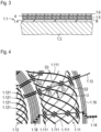
- the scanning element 1 comprises a circuit board 1.1, which according to the Figure 3 has several layers A, B, here exactly two layers A, B.
- the circuit board 1.1 is designed to be very thin with a Thickness of approx. 100 ⁇ m, which is why it can also be referred to as a film.
- the circuit board 1.1 is applied here to a comparatively thick substrate 1.3, which can in particular consist of a metallic material.
- an electrically insulating layer 1.4 Arranged on this substrate 1.3 is an electrically insulating layer 1.4 with a thickness of approximately 50 ⁇ m, on which the second layer B is applied.
- Another approximately 15 ⁇ m thick insulating layer 1.5 is located between the second layer B and the first layer A.
- insulating layer 1.6 which is also approximately 15 ⁇ m thick.
- the two layers A, B are each approx. 12 ⁇ m thick.
- the insulating layers 1.4, 1.5, 1.6 are made of polyimide in the exemplary embodiment presented.
- the scanning element 1 is used to scan the scale element 2.
- the circuit board 1.1 comprises a first (inner) exciter conductor track 1.18 and a second exciter conductor track 1.19.
- the exciter conductor tracks 1.18, 1.19 run in the first layer A and in the second layer B.
- a first receiver track 1.11 and a second receiver track 1.12 are arranged on the circuit board 1.1.
- the excitation conductor tracks 1.18, 1.19 enclose the second receiver track 1.12 or the first receiver track 1.11 and run along the measuring direction U or along the circumferential direction.
- each of the receiver tracks 1.11, 1.12 includes receiver conductor tracks 1.111, 1.121 (see for example Figure 4 ), which are arranged offset in the circumferential direction so that they can deliver four phase-shifted signals corresponding to the offset.
- those receiver conductor tracks 1.111, 1.121 which belong to one and the same receiver track 1.11, 1.12 are provided with only one reference number. Consequently, for example, all receiver conductor tracks 1.111 of the first receiver track 1.11 are provided with only one reference number.
- the first receiver conductor tracks 1.111 of the first receiver track 1.11 are connected to vias in the different layers A, B of the circuit board 1.1, so that undesirable short circuits are avoided at crossing points. The same applies to the receiver conductor tracks 1.121 the second receiver track 1.12.
- each of the first and second receiver conductor tracks 1.111, 1.121 consists of many conductor pieces, which are each distributed and lined up on two levels or layers A, B, such a structure is referred to below collectively as a receiver conductor track 1.111, 1.121.
- the conductor tracks in the areas where conductor tracks only run in the first layer A are shown in black.
- conductor tracks in the areas where conductor tracks only run in the second layer B are shown in white with a black border line.
- conductor tracks are shown in black and white dashed lines in the areas in which conductor tracks run one above the other in the first layer A and in the second layer B.
- the receiver conductor tracks 1.111, 1.121 have a spatially periodic course that is essentially sinusoidal or sinusoidal.
- the receiver conductor tracks 1.111 of the first receiver track 1.11 have a period length ⁇ 1 ( Figure 1 ), while the receiver conductor tracks 1.121 of the second receiver track 1.12 have a period length ⁇ 2.
- adjacent receiver conductor tracks 1.111, 1.121 are arranged offset from one another by 1/8 of the full sine period (by ⁇ /4 or 45 ° along the circumferential direction or measuring direction U).
- the receiver conductor tracks 1.111, 1.121 are electrically connected in such a way that they deliver 0° and 90° signals on the one hand and 45° and 135° signals on the other.
- a first position signal can be determined from the 0° and 90° signals and a second position signal that is redundant with respect to the first position signal can be determined from the 45° and 135° signals.
- the scanning element 1 has an electronic circuit with a large number of electronic components 1.2, which are in the Figure 1 are only shown schematically.
- the electronic circuit also includes an ASIC component.
- the signals received from the second receiver track 1.12 must be routed to the electronic circuit, in particular to an area that serves as an evaluation circuit.
- the first ladder route 1.131 ( Figure 5 ) is at a first point, for example at a first end of the second receiver conductor track 1.121 ( Figure 4 ), with the second receiver conductor track 1.121 electrically connected or contacted. This first point is in the first layer A of the circuit board 1.1.
- the second conductor track 1.132 is electrically connected or contacted with the second receiver conductor track 1.121 at another second point, for example at a second end of the second receiver conductor track 1.121.
- This other second point is located in the second layer B of the circuit board 1.1, whereby in the exemplary embodiment presented, the first point of the first conductor track 1.131 and the other second point of the second conductor track 1.132 lie one above the other in the layer structure of the circuit board 1.1.
- the circuit board 1.1 also has a further connection line 1.14, which also includes a first conductor track 1.141 and a second conductor track 1.142.
- the first conductor track 1.141 is electrically connected or contacted with the first exciter conductor track 1.18 at a third point, for example at a first end of the first exciter conductor track 1.18. This third point is in the first layer A of the circuit board 1.1.
- the second conductor track 1.142 is electrically connected or contacted with the first exciter conductor track 1.18 at another fourth point, for example at a second end of the first exciter conductor track 1.18.
- This other fourth point is located in the second layer B of the circuit board 1.1, where in the exemplary embodiment presented the third point of the first conductor track 1.141 and the other fourth point of the second conductor track 1.142 lie one above the other. With this configuration, the first excitation conductor track 1.18 is supplied with the excitation current.
- the circuit board 1.1 is designed such that the connecting lines 1.13, 1.14 cross the first receiver track 1.11. In this context, it is important that the connection line 1.13 to the second receiver track 1.12 does not capture any disturbing signals that could be picked up when crossing the first receiver track 1.11. It should also be avoided that the excitation currents for the first excitation conductor track 1.18, which flow through the connecting line 1.14, cause significant interference in the first receiver track 1.11.
- the course of the connecting line 1.13 is designed so that according to Figure 5
- the first conductor trace 1.131 and the second conductor trace 1.132 run such that the first conductor trace 1.131 is arranged offset from the second conductor trace 1.132 in the positive measuring direction U+.
- the second conductor track 1.132 is arranged offset from the first conductor track 1.131 in the positive measuring direction U+.
- the first conductor track 1.131 and the second conductor track 1.132 are arranged one above the other in the first layer A and in the second layer B in third sections S3 of the connecting line 1.13.
- the conductor tracks 1.131, 1.132 therefore run in sections in the first layer A and in sections in the second layer B.
- the change between layers A, B is carried out in the first conductor track 1.131 through vias 1.1311 and in the second conductor track 1.132 through vias 1.1321.
- the connecting line 1.14 which is used to connect the first excitation conductor track 1.18, can be explained.
- the first conductor track 1.141 and the second conductor track 1.142 run in such a way that the first conductor track 1.141 is arranged offset from the second conductor track 1.142 in the positive measuring direction U+.
- the second conductor track is in a second section S2 of the connecting line 1.14 1.142 arranged offset from the first conductor track 1.141 in the positive measuring direction U+.
- the first conductor track 1.141 and the second conductor track 1.142 are arranged one above the other in the first layer A and in the second layer B in third sections S3 of the connecting line 1.14. This means that the first conductor track 1.141 and the second conductor track 1.142 are arranged one above the other in a direction orthogonal to the circuit board 1.1.
- the third sections S3 extend in total over the largest portion of the length of the connecting line 1.14.
- the Figure 7 For the spatial representation of the courses of the first and second conductor tracks 1.141, 1.142 the Figure 7 be used. Going from the left in this figure, the first conductor track 1.141 in the first layer A of the circuit board 1.1 and the second conductor track 1.142 in the second layer B run one above the other in a section S3. This arrangement, which is inherently immune to interference, cannot be maintained in the further course because the connecting line 1.14 has to cross the first receiver track 1.11.
- the courses of the first and second conductor tracks 1.141, 1.142 are therefore initially changed so that they are aligned in both layers A, B along a section parallel to the first receiver conductor tracks 1.111 in the same position A, B.
- the first conductor track 1,141 in the first layer A crosses a first receiver conductor track 1,111, which runs there in the second layer B.
- the second conductor track 1.142 running in the second layer B crosses a first receiver conductor track 1.111, which runs there in the first layer A.
- the first and second conductor tracks 1.141, 1.142 run in these sections up to vias 1.1411, 1.1412, where the first and second conductor tracks 1.141, 1.142 then change from the first layer A to the second layer B of the circuit board 1.1 or vice versa.
- the first and second conductor tracks 1.141, 1.142 are again oriented parallel to the respective first receiver conductor track 1.111, whereby the parallelism refers to the first receiver conductor track 1.111 in the same position A, B in which the first and second Conductor route 1.141, 1.142 runs.
- the first and second conductor tracks 1,141, 1,142 re-enter a third section S3, where they are arranged one above the other.
- the scale element 2 which has a disk-shaped shape, is shown in a top view.
- the scale element 2 consists of a carrier, which in the illustrated embodiment is made of epoxy resin, and on which two graduation tracks 2.1, 2.2 are arranged.
- the dividing tracks 2.1, 2.2 are ring-shaped and arranged concentrically with different diameters on the carrier with respect to the axis R.
- the division tracks 2.1, 2.2 include division structures each consisting of a periodic sequence of alternately arranged electrically conductive division areas 2.11, 2.21 and non-conductive division areas 2.12, 2.22. In the example shown, copper was applied to the carrier as the material for the electrically conductive division areas 2.11, 2.21.
- the carrier was not coated. Due to the arrangement with two graduation tracks 2.1, 2.2, the angular position of the scale element 2 can be determined absolutely.
- the outermost graduation track 2.1 of the scale element 2 has the larger number of graduation areas 2.11, 2.12 along a circumferential line, so that the greatest resolution with regard to the measurement of the angular position can be achieved.
- the scanning element 1 and the scale element 2 face each other with an axial distance or air gap, so that when there is a relative rotation between the scale element 2 and the scanning element 1 in the receiver conductor tracks 1.111, 1.121, a signal dependent on the respective angular position can be generated by induction effects .
- the prerequisite for the formation of corresponding signals is that the excitation conductor tracks 1.18, 1.19 generate a time-changing electromagnetic excitation field in the area of the respective scanned division structures.
- the exciter conductor tracks 1.18, 1.19 are designed as several planar-parallel current-carrying individual conductor tracks.
- the electronic circuit of the scanning element 1 works not only as an evaluation element, but also as an excitation control element, under whose control the excitation current is generated or generated, which then flows through the excitation conductor tracks 1.18, 1.19. Thus become the exciter conductor tracks 1.18, 1.19 are energized by one and the same exciter control element via the connecting line 1.14.
- the first exciter conductor track 1.18 and the second exciter conductor track 1.19 are electrically connected in series.
- an electromagnetic field oriented in the shape of a tube or cylinder is formed around them.
- the field lines of the resulting electromagnetic field run around the exciter conductor tracks 1.18, 1.19, the direction of the field lines depending in a known manner on the direction of the current in the exciter conductor tracks 1.18, 1.19.
- Eddy currents are induced in the area of the conductive subregions 2.11, 2.21, so that a modulation of the field that is dependent on the angular position is achieved. Accordingly, the relative angular position can be measured by the receiver tracks 1.11, 1.12.
- the receiver conductor tracks 1.111, 1.121 are arranged within their receiver tracks 1.11, 1.12 in such a way that they each deliver signals that are 90° out of phase, so that the direction of rotation can also be determined.
- the signals generated by the receiver tracks 1.11, 1.12 are further processed by an evaluation circuit.
- FIG. 8 and 9 show a connection line 1.13 'comprising a first conductor track 1.131' and a second conductor track 1.132', the first conductor track 1.131' being electrically connected to the second receiver conductor track 1.121 at one point and the second conductor track 1.132' being electrically connected to the second receiver conductor track 1.121 at another point .
- the scanning element 1 ' according to the second exemplary embodiment also includes a further connection line to the excitation conductor track 1.18; this connection line is not shown in the figures.
- the first conductor track 1.131' and the second conductor track 1.132' run in such a way that in several first sections S1' (here three) of the connecting line 1.13' first conductor track 1.131' is arranged offset from the second conductor track 1.132' in the positive measuring direction U+.
- first sections S1' are located adjacent to one another in the course of the connecting line 1.13'.
- second conductor track 1.132' is arranged offset from the first conductor track 1.131' in the positive measuring direction U+, the second sections S2' being arranged adjacent to one another.
Landscapes
- Physics & Mathematics (AREA)
- General Physics & Mathematics (AREA)
- Transmission And Conversion Of Sensor Element Output (AREA)
- Measurement Of Length, Angles, Or The Like Using Electric Or Magnetic Means (AREA)
- Structure Of Printed Boards (AREA)
Abstract
Die Erfindung betrifft ein Abtastelement (1; 1'), zur Messung einer Position entlang einer Messrichtung (U), das eine mehrlagige Leiterplatte (1.1; 1.1') umfasst. Die Leiterplatte (1.1; 1.1') weist eine erste Empfängerspur (1.11) auf, die eine erste Empfängerleiterbahn (1.111) umfasst. Die Leiterplatte (1.1; 1.1') weist zudem eine Anschlussleitung (1.13; 1.13', 1.14) auf, welche einen ersten Leiterzug (1.131; 1.131', 1.141) und einen zweiten Leiterzug (1.132; 1.132', 1.142) umfasst, wobei die Anschlussleitung (1.13; 1.13', 1.14) die erste Empfängerspur (1.11) kreuzt. Der erste Leiterzug (1.131; 1.131', 1.141) und der zweite Leiterzug (1.132; 1.132', 1.142) verlaufen so, dass in zumindest einem ersten Abschnitt (S1; S1') der Anschlussleitung (1.13; 1.13', 1.14) der erste Leiterzug (1.131; 1.131', 1.141) in positiver Messrichtung (U+) versetzt zum zweiten Leiterzug (1.132; 1.132', 1.142) angeordnet ist und in zumindest einem zweiten Abschnitt (S2; S2') der Anschlussleitung (1.13; 1.13', 1.14) der zweite Leiterzug (1.132; 1.132', 1.142) in positiver Messrichtung (U+) versetzt zum ersten Leiterzug (1.131; 1.131', 1.141) angeordnet ist. (Figur 7)The invention relates to a scanning element (1; 1') for measuring a position along a measuring direction (U), which comprises a multi-layer printed circuit board (1.1; 1.1'). The circuit board (1.1; 1.1') has a first receiver track (1.11), which includes a first receiver conductor track (1.111). The circuit board (1.1; 1.1') also has a connection line (1.13; 1.13', 1.14), which comprises a first conductor track (1.131; 1.131', 1.141) and a second conductor track (1.132; 1.132', 1.142), the Connection line (1.13; 1.13 ', 1.14) crosses the first receiver track (1.11). The first conductor run (1.131; 1.131', 1.141) and the second conductor run (1.132; 1.132', 1.142) run such that in at least a first section (S1; S1') of the connecting line (1.13; 1.13', 1.14) the first Conductor track (1.131; 1.131', 1.141) is arranged offset in the positive measuring direction (U+) from the second conductor track (1.132; 1.132', 1.142) and in at least a second section (S2; S2') of the connecting line (1.13; 1.13', 1.14 ) the second conductor track (1.132; 1.132', 1.142) is arranged offset from the first conductor track (1.131; 1.131', 1.141) in the positive measuring direction (U+). (Figure 7)
Description
Die Erfindung betrifft ein Abtastelement für eine induktive Positionsmesseinrichtung gemäß dem Anspruch 1 zur Positionsbestimmung des Abtastelements relativ zu einem Skalenelement sowie eine Positionsmesseinrichtung mit einem derartigen Abtastelement.The invention relates to a scanning element for an inductive position measuring device according to
Induktive Positionsmesseinrichtungen werden beispielsweise als Winkelmessgeräte zur Bestimmung der Winkelposition von relativ zueinander drehbaren Maschinenteilen verwendet. Bei induktiven Positionsmesseinrichtungen sind häufig Erregerspuren und Empfängerspuren etwa in Form von Leiterbahnen auf einer gemeinsamen meist mehrlagigen Leiterplatte aufgebracht, die beispielsweise mit einem Stator eines Winkelmessgeräts fest verbunden ist. Dieser Leiterplatte gegenüber befindet sich ein Skalenelement, auf dem Teilungsstrukturen aufgebracht sind, und welches mit dem Rotor des Winkelmessgeräts drehfest verbunden ist. Wenn an den Erregerleiterbahnen ein zeitlich wechselnder elektrischer Erregerstrom angelegt wird, werden in den Empfängerspulen während der Relativdrehung zwischen Rotor und Stator von der Winkelposition abhängige Signale erzeugt. Diese Signale werden dann in einer Auswerteelektronik weiterverarbeitet.Inductive position measuring devices are used, for example, as angle measuring devices to determine the angular position of machine parts that can rotate relative to one another. In inductive position measuring devices, exciter tracks and receiver tracks are often applied in the form of conductor tracks on a common, usually multi-layer circuit board, which is firmly connected, for example, to a stator of an angle measuring device. Opposite this circuit board there is a scale element on which graduation structures are applied and which is connected in a rotationally fixed manner to the rotor of the angle measuring device. If a time-changing electrical excitation current is applied to the excitation conductor tracks, The receiver coils generate signals that depend on the angular position during the relative rotation between the rotor and stator. These signals are then further processed in evaluation electronics.
Häufig werden derartige induktive Winkelmesseinrichtungen als Messgeräte für elektrische Antriebe, zur Bestimmung der Relativbewegung beziehungsweise der Relativlage von entsprechenden Maschinenteilen eingesetzt. In diesem Fall werden die erzeugten Winkelpositionswerte einer Folgeelektronik zur Ansteuerung der Antriebe über eine entsprechende Schnittstellenanordnung zugeführt.Such inductive angle measuring devices are often used as measuring devices for electric drives to determine the relative movement or the relative position of corresponding machine parts. In this case, the generated angular position values are fed to subsequent electronics for controlling the drives via a corresponding interface arrangement.
Ferner werden induktive Positionsmesseinrichtungen häufig auch zur direkten Messung von Längsverschiebungen entlang einer Achse verwendet. Dabei wird das gleiche Messprinzip angewendet wie bei den oben genannten Winkelmessgeräten, allerdings verlaufen dann die Empfängerspulen und die Teilungsstruktur entlang der geradlinigen Achse.Furthermore, inductive position measuring devices are often used for direct measurement of longitudinal displacements along an axis. The same measuring principle is used as with the angle measuring devices mentioned above, but the receiver coils and the graduation structure then run along the straight axis.
Aus der
In der
Der Erfindung liegt die Aufgabe zugrunde ein vergleichsweise genau arbeitendes, kompaktes und kostengünstig herstellbares Abtastelement für eine induktive Positionsmesseinrichtung zu schaffen.The invention is based on the object of creating a comparatively precisely operating, compact and inexpensively producible scanning element for an inductive position measuring device.
Diese Aufgabe wird erfindungsgemäß durch die Merkmale des Anspruches 1 gelöst.This object is achieved according to the invention by the features of
Das Abtastelement, welches für eine induktive Positionsmesseinrichtung zur Messung einer Position entlang einer Messrichtung geeignet und bestimmt ist, umfasst eine Leiterplatte, die eine erste Lage und eine zweite Lage aufweist. Zudem weist die Leiterplatte eine erste Empfängerspur auf, die zumindest eine erste Empfängerleiterbahn umfasst und zumindest eine Anschlussleitung, welche einen ersten Leiterzug und einen zweiten Leiterzug umfasst. Die Anschlussleitung kreuzt beziehungsweise durchquert die erste Empfängerspur. Weiterhin weist die Leiterplatte eine zweite Empfängerspur auf, die zumindest eine zweite Empfängerleiterbahn umfasst. Der erste Leiterzug ist an einem (ersten) Punkt mit der zweiten Empfängerleiterbahn elektrisch verbunden und der zweite Leiterzug ist an einem anderen (zweiten) Punkt mit der zweiten Empfängerleiterbahn elektrisch verbunden, so dass ein Signal, das durch die zweite Empfängerleiterbahn empfangen wurde, mit Hilfe der Leiterzüge abgreifbar ist. Alternativ oder ergänzend weist die Leiterplatte eine erste Erregerleiterbahn auf, wobei der erste Leiterzug an einem (dritten) Punkt mit der ersten Erregerleiterbahn elektrisch verbunden ist und der zweite Leiterzug an einem anderen (vierten) Punkt mit der ersten Erregerleiterbahn elektrisch verbunden ist, so dass über den ersten Leiterzug und über den zweiten Leiterzug ein Erregerstrom in die erste Erregerleiterbahn einleitbar ist. Der erste Leiterzug und der zweite Leiterzug verlaufen so, dass in zumindest einem ersten Abschnitt der Anschlussleitung der erste Leiterzug in positiver Messrichtung versetzt zum zweiten Leiterzug angeordnet ist und in zumindest einem zweiten Abschnitt der Anschlussleitung der zweite Leiterzug in positiver Messrichtung versetzt zum ersten Leiterzug angeordnet ist.The scanning element, which is suitable and intended for an inductive position measuring device for measuring a position along a measuring direction, comprises a circuit board which has a first layer and a second layer. In addition, the circuit board has a first receiver track, which comprises at least a first receiver conductor track and at least one connecting line, which comprises a first conductor track and a second conductor track. The connecting line crosses or passes through the first receiver track. Furthermore, the circuit board has a second receiver track, which includes at least a second receiver conductor track. The first conductor trace is electrically connected to the second receiver conductor trace at a (first) point and the second conductor trace is electrically connected to the second receiver conductor trace at another (second) point, so that a signal received by the second receiver conductor trace is with the help the conductor tracks can be picked up. Alternatively or additionally, the circuit board has a first excitation conductor track, wherein the first conductor track is electrically connected to the first excitation conductor track at a (third) point and the second conductor track is electrically connected to the first excitation conductor track at another (fourth) point, so that via the first conductor track and an excitation current can be introduced into the first excitation conductor track via the second conductor track. The first conductor track and the second conductor track run in such a way that in at least a first section of the connecting line the first conductor track is arranged offset in the positive measuring direction from the second conductor track and in at least a second section of the connecting line the second conductor track is arranged offset in the positive measuring direction from the first conductor track .
Die Messrichtung kann eine lineare Richtung oder eine Umfangsrichtung beziehungsweise eine Tangentialrichtung sein. Als positive Messrichtung kann bei einer linearen Messung beispielsweise eine Richtung (relative Verschiebung) nach links verstanden werden und demnach kann als negative Messrichtung die Richtung nach rechts gesehen werden. Bei einer Messung einer Winkelposition, also in Umfangsrichtung, kann beispielsweise als die positive Messrichtung eine Messrichtung in Richtung des Uhrzeigersinns und als negative Messrichtung eine Messrichtung in Richtung entgegen des Uhrzeigersinns definiert werden. Insbesondere verläuft die erste Erregerleiterbahn entlang der Umfangsrichtung beziehungsweise entlang der Messrichtung.The measuring direction can be a linear direction or a circumferential direction or a tangential direction. In a linear measurement, for example, a direction (relative displacement) to the left can be understood as a positive measuring direction and the direction to the right can therefore be seen as a negative measuring direction. When measuring an angular position, i.e. in the circumferential direction, a clockwise measuring direction can be used as the positive measuring direction and a negative measuring direction can be used Measuring direction can be defined as a measuring direction in the counterclockwise direction. In particular, the first exciter conductor track runs along the circumferential direction or along the measuring direction.
Mit Vorteil verlaufen die erste Empfängerspur und die zweite Empfängerspur entlang der Umfangsrichtung beziehungsweise entlang der Messrichtung wie auch die erste Erregerleiterbahn.The first receiver track and the second receiver track advantageously run along the circumferential direction or along the measuring direction, as does the first excitation conductor track.
In weiterer Ausgestaltung der Erfindung befinden sich der (erste) Punkt, an dem der erste Leiterzug mit der zweiten Empfängerleiterbahn elektrisch verbunden ist, in der ersten Lage und der andere (zweite) Punkt, an dem der zweite Leiterzug mit der zweiten Empfängerleiterbahn elektrisch verbunden ist, in der zweiten Lage der Leiterplatte. Alternativ oder ergänzend befinden sich der (dritte) Punkt, an dem der erste Leiterzug mit der ersten Erregerleiterbahn elektrisch verbunden ist, in der ersten Lage und der andere (vierte) Punkt, an dem der zweite Leiterzug mit der ersten Erregerleiterbahn elektrisch verbunden ist, in der zweiten Lage.In a further embodiment of the invention, the (first) point at which the first conductor track is electrically connected to the second receiver conductor track is in the first position and the other (second) point at which the second conductor track is electrically connected to the second receiver conductor track is in the first position , in the second layer of the circuit board. Alternatively or additionally, the (third) point at which the first conductor track is electrically connected to the first exciter conductor track is in the first position and the other (fourth) point at which the second conductor track is electrically connected to the first exciter conductor track is in the second layer.
In vorteilhafter Ausgestaltung der Erfindung verlaufen streckenweise im ersten Abschnitt die erste Empfängerleiterbahn und der erste oder der zweite Leiterzug parallel zueinander in derselben Lage der Leiterplatte. Alternativ oder ergänzend verlaufen streckenweise im zweiten Abschnitt die erste Empfängerleiterbahn und der erste oder der zweite Leiterzug parallel zueinander in derselben Lage der Leiterplatte.In an advantageous embodiment of the invention, in the first section the first receiver conductor track and the first or second conductor track run parallel to one another in the same position of the circuit board. Alternatively or additionally, in the second section, the first receiver conductor track and the first or second conductor track run parallel to one another in the same position of the circuit board.
Mit Vorteil sind in zumindest einem dritten Abschnitt der Anschlussleitung der erste Leiterzug in der ersten Lage und der zweite Leiterzug in der zweiten Lage übereinander verlaufend angeordnet. Der Begriff übereinander ist so zu verstehen, dass die Leiterzüge in einer Richtung orthogonal zur Leiterplatte übereinander mit parallelem Verlauf angeordnet sind.Advantageously, in at least a third section of the connecting line, the first conductor run in the first layer and the second conductor run in the second layer are arranged one above the other. The term one above the other is to be understood as meaning that the conductor tracks are arranged one above the other in a direction orthogonal to the circuit board with a parallel course.
In weiterer Ausgestaltung der Erfindung verlaufen im ersten Abschnitt und / oder im zweiten Abschnitt der erste Leiterzug und der zweite Leiterzug streckenweise zueinander parallel. In diesem Fall kann die erste Empfängerleiterbahn insbesondere mittig zwischen den parallel verlaufenden ersten und zweiten Leiterzügen in derselben Lage wie die Leiterzüge verlaufen.In a further embodiment of the invention, the first conductor track and the second conductor track run parallel to one another in sections in the first section and/or in the second section. In this case, the first receiver conductor track can in particular run centrally between the parallel first and second conductor tracks in the same position as the conductor tracks.
Mit Vorteil wechseln der Verlauf des ersten Leiterzugs und der Verlauf des zweiten Leiterzugs im ersten Abschnitt und / oder im zweiten Abschnitt von der ersten Lage auf die zweite Lage.The course of the first conductor track and the course of the second conductor track advantageously change from the first layer to the second layer in the first section and/or in the second section.
In vorteilhafter Ausgestaltung der Erfindung verläuft der erste Leiterzug im ersten Abschnitt entlang einer Teilstrecke in der ersten Lage und die erste Empfängerleiterbahn verläuft in diesem Bereich ebenfalls in der ersten Lage. In dieser Teilstrecke verläuft der erste Leiterzug parallel zur ersten Empfängerleiterbahn. Optional umfasst die erste Empfängerspur eine weitere erste Empfängerleiterbahn, die im ersten Abschnitt in der zweiten Lage verläuft, wobei der erste Leiterzug die weitere erste Empfängerleiterbahn in der Teilstrecke kreuzt.In an advantageous embodiment of the invention, the first conductor track in the first section runs along a partial route in the first position and the first receiver conductor track also runs in the first position in this area. In this section, the first conductor track runs parallel to the first receiver conductor track. Optionally, the first receiver track comprises a further first receiver conductor track, which runs in the second layer in the first section, the first conductor track crossing the further first receiver conductor track in the section.
Als Lage der Leiterplatte ist hier, wie in der Leiterplattentechnologie üblich, eine elektrisch leitende Lage beziehungsweise Schicht zu verstehen. Die Leiterplatte kann als eine starre Leiterplatte mit beispielsweise einem FR4-Kern ausgestaltet sein. Alternativ kann die Leiterplatte als eine dünne Flexleiterplatte beziehungsweise Leiterfolie z. B. auf Basis von Polyimid-Folien ausgestaltet sein. Die Leiterplatte kann eine Dicke von weniger als 1 mm, mit Vorteil weniger als 500µm, insbesondere weniger als 200 µm aufweisen. Gerade bei einer geringen Dicke der Leiterplatte kann es vorteilhaft sein, wenn diese auf einem vergleichsweise starken Metallsubstrat aufgebracht ist.As is usual in circuit board technology, the layer of the circuit board here is understood to mean an electrically conductive layer or layer. The circuit board can be designed as a rigid circuit board with, for example, an FR4 core. Alternatively, the circuit board can be used as a thin flexible circuit board or conductor foil, for example. B. be designed based on polyimide films. The circuit board can have a thickness of less than 1 mm, advantageously less than 500 μm, in particular less than 200 μm. Especially if the circuit board is thin, it can be advantageous if it is applied to a comparatively strong metal substrate.
Mit Vorteil ist die erste Erregerleiterbahn mit einem Erregerstrom bestrombar, welcher üblicherweise eine zeitlich wechselnde Stromstärke aufweist (Wechselstrom oder Mischstrom). Der Erregerstrom ist mit Hilfe elektronischer Bauteile generierbar, das heißt, dass dessen Verlauf von den elektronischen Bauteilen formbar ist. Nachdem ein physikalischer Zusammenhang zwischen der Stromstärke und der Spannungsstärke existiert, kann natürlich die gleiche Betrachtung auch für die Erregerspannung vorgenommen werden. Die elektronischen Bauteile können auf der Leiterplatte montiert sein. In weiterer Ausgestaltung der Erfindung sind diejenigen Signale, die von der ersten Empfängerspur und der zweiten Empfängerspur erzeugbar sind, mit Hilfe der elektronischen Bauteile, die insbesondere eine Auswerteschaltung bilden, weiterverarbeitbar.Advantageously, the first excitation conductor track can be energized with an excitation current, which usually has a current intensity that changes over time (alternating current or mixed current). The excitation current can be generated with the help of electronic components, which means that its course can be shaped by the electronic components. Since there is a physical connection between the current strength and the voltage strength, the same consideration can of course also be made for the excitation voltage. The electronic components can be mounted on the circuit board. In a further embodiment of the invention, those signals that can be generated by the first receiver track and the second receiver track can be further processed with the help of the electronic components, which in particular form an evaluation circuit.
Die elektronischen Bauteile können also Elemente verschiedener elektronischer Schaltungen sein beziehungsweise unterschiedlichen Schaltungen zugeordnet sein. Beispielsweise können bestimmte elektronische Bauteile Elemente der Schaltung zur Generierung eines Erregerstroms sein oder weitere elektronische Bauteile können Elemente einer weiteren Schaltung zur Auswertung beziehungsweise Weiterverarbeitung von Signalen sein.The electronic components can therefore be elements of different electronic circuits or assigned to different circuits. For example, certain electronic components can be elements of the circuit for generating an excitation current or further electronic components can be elements of a further circuit for evaluating or further processing signals.
In weiterer Ausgestaltung der Erfindung weist die Leiterplatte genau zwei Lagen auf. Insbesondere kann das Abtastelement ein Substrat aufweisen, auf dem die Leiterplatte angeordnet beziehungsweise aufgebracht ist.In a further embodiment of the invention, the circuit board has exactly two layers. In particular, the scanning element can have a substrate on which the circuit board is arranged or applied.
Mit Vorteil ist das Substrat aus einem metallischen Werkstoff hergestellt, insbesondere als ein Blech ausgestaltet. Beispielsweise kann das Substrat aus einem weichmagnetischen Werkstoff hergestellt sein.The substrate is advantageously made of a metallic material, in particular designed as a sheet of metal. For example, the substrate can be made from a soft magnetic material.
In vorteilhafter Ausgestaltung der Erfindung sind die erste Empfängerspur und die zweite Empfängerspur um eine Achse gekrümmt angeordnet, wobei die erste Empfängerspur bezüglich der Achse radial außen relativ zur zweiten Empfängerspur angeordnet ist. Ein derartiges Abtastelement dient insbesondere zur Bestimmung einer Winkelposition. Insbesondere können die erste Empfängerspur und die zweite Empfängerspur lückenlos über 360° um die Achse umlaufend angeordnet und ausgestaltet sein.In an advantageous embodiment of the invention, the first receiver track and the second receiver track are arranged curved about an axis, with the first receiver track being arranged radially on the outside relative to the second receiver track with respect to the axis. Such a scanning element is used in particular to determine an angular position. In particular, the first receiver track and the second receiver track can be arranged and designed to run continuously over 360° around the axis.
Gemäß einem weiteren Aspekt umfasst die Erfindung auch eine induktive Positionsmesseinrichtung mit dem Abtastelement sowie einem Skalenelement, wobei das Skalenelement in einer Richtung, die orthogonal zur Messrichtung orientiert ist, beabstandet zur Leiterplatte angeordnet ist.According to a further aspect, the invention also includes an inductive position measuring device with the scanning element and a scale element, wherein the scale element is arranged at a distance from the circuit board in a direction that is oriented orthogonally to the measuring direction.
Vorteilhafte Ausbildungen der Erfindung entnimmt man den abhängigen Ansprüchen.Advantageous embodiments of the invention can be found in the dependent claims.
Weitere Einzelheiten und Vorteile des erfindungsgemäßen Abtastelements ergeben sich aus der nachfolgenden Beschreibung zweier Ausführungsbeispiele anhand der beiliegenden Figuren.Further details and advantages of the scanning element according to the invention result from the following description of two exemplary embodiments based on the accompanying figures.
- Figur 1Figure 1
- eine Draufsicht auf eine Seite eines Abtastelements,a top view of one side of a scanning element,
- Figur 2Figure 2
- eine Draufsicht auf eine Seite eines Skalenelements,a top view of one side of a scale element,
- Figur 3Figure 3
- eine Teilschnitt-Ansicht des Abtastelements,a partial section view of the scanning element,
- Figur 4Figure 4
- eine Detailansicht auf das Abtastelement mit Anschlussleitungen,a detailed view of the scanning element with connecting cables,
- Figur 5Figure 5
- eine Detailansicht auf eine der Anschlussleitungen,a detailed view of one of the connecting cables,
- Figur 6Figure 6
- eine Detailansicht auf eine andere Anschlussleitung,a detailed view of another connecting cable,
- Figur 7Figure 7
- eine räumliche Ansicht auf ein Detail der Anschlussleitung,a spatial view of a detail of the connection line,
- Figur 8Figure 8
- eine Detailansicht auf das Abtastelement mit Anschlussleitung gemäß einem zweiten Ausführungsbeispiel,a detailed view of the scanning element with connecting cable according to a second exemplary embodiment,
- Figur 9Figure 9
- eine Detailansicht auf die Anschlussleitung, gemäß dem zweiten Ausführungsbeispiel.a detailed view of the connecting cable, according to the second exemplary embodiment.
Die Erfindung wird gemäß den
Das Abtastelement 1 umfasst eine Leiterplatte 1.1, welche gemäß der
Die Leiterplatte 1.1 umfasst eine erste (innere) Erregerleiterbahn 1.18 und eine zweite Erregerleiterbahn 1.19. Die Erregerleiterbahnen 1.18, 1.19 verlaufen in der ersten Lage A und in der zweiten Lage B.The circuit board 1.1 comprises a first (inner) exciter conductor track 1.18 and a second exciter conductor track 1.19. The exciter conductor tracks 1.18, 1.19 run in the first layer A and in the second layer B.
Zur Bestimmung der Winkelinformationen sind auf der Leiterplatte 1.1 eine erste Empfängerspur 1.11 und eine zweite Empfängerspur 1.12 angeordnet. Die Erregerleiterbahnen 1.18, 1.19 umschließen die zweite Empfängerspur 1.12 beziehungsweise die erste Empfängerspur 1.11 und verlaufen entlang der Messrichtung U beziehungsweise entlang der Umfangsrichtung.To determine the angle information, a first receiver track 1.11 and a second receiver track 1.12 are arranged on the circuit board 1.1. The excitation conductor tracks 1.18, 1.19 enclose the second receiver track 1.12 or the first receiver track 1.11 and run along the measuring direction U or along the circumferential direction.
Jede der Empfängerspuren 1.11, 1.12 umfasst im vorgestellten Ausführungsbeispiel jeweils Empfängerleiterbahnen 1.111, 1.121 (siehe etwa die
Die Empfängerleiterbahnen 1.111, 1.121 weisen einen räumlich periodischen Verlauf auf, der im Wesentlichen sinusförmig beziehungsweise sinusartig ausgestaltet ist. Die Empfängerleiterbahnen 1.111 der ersten Empfängerspur 1.11 weisen eine Periodenlänge λ1 (
Im vorgestellten Ausführungsbeispiel ist die zweite Periodenlänge λ2 kleiner als die erste Periodenlänge λ1 (λ2/λ1 = 7/8).In the exemplary embodiment presented, the second period length λ2 is smaller than the first period length λ1 (λ2/λ1 = 7/8).
Das Abtastelement 1 weist eine elektronische Schaltung mit einer Vielzahl von elektronischen Bausteinen 1.2 auf, die in der
Die von der zweiten Empfängerspur 1.12 empfangenen Signale müssen zur elektronischen Schaltung, insbesondere zu einem Bereich, der als Auswerteschaltung dient, geführt werden. Zu diesem Zweck befinden sich auf der Leiterplatte vier Anschlussleitungen 1.13, welche jeweils einen ersten Leiterzug 1.131 und einen zweiten Leiterzug 1.132 aufweisen.The signals received from the second receiver track 1.12 must be routed to the electronic circuit, in particular to an area that serves as an evaluation circuit. For this purpose, there are four connecting lines 1.13 on the circuit board, each of which has a first conductor track 1.131 and a second conductor track 1.132.
Der erste Leiterzug 1.131 (
Damit die erste Erregerleiterbahn 1.18 mit dem Erregerstrom versorgt werden kann, weist die Leiterplatte 1.1 zudem eine weitere Anschlussleitung 1.14 auf, die ebenfalls einen ersten Leiterzug 1.141 und einen zweiten Leiterzug 1.142 umfasst. Der erste Leiterzug 1.141 ist an einem dritten Punkt, zum Beispiel an einem ersten Ende der ersten Erregerleiterbahn 1.18, mit der ersten Erregerleiterbahn 1.18 elektrisch verbunden beziehungsweise kontaktiert. Dieser dritte Punkt befindet sich in der ersten Lage A der Leiterplatte 1.1. Zudem ist der zweite Leiterzug 1.142 an einem anderen vierten Punkt, zum Beispiel an einem zweiten Ende der ersten Erregerleiterbahn 1.18 mit der ersten Erregerleiterbahn 1.18 elektrisch verbunden beziehungsweise kontaktiert. Dieser andere vierte Punkt befindet sich in der zweiten Lage B der Leiterplatte 1.1, wobei im vorgestellten Ausführungsbeispiel der dritte Punkt des ersten Leiterzugs 1.141 und der andere vierte Punkt des zweiten Leiterzugs 1.142 übereinander liegen. Mit dieser Konfiguration wird die erste Erregerleiterbahn 1.18 mit dem Erregerstrom versorgt.So that the first excitation conductor track 1.18 can be supplied with the excitation current, the circuit board 1.1 also has a further connection line 1.14, which also includes a first conductor track 1.141 and a second conductor track 1.142. The first conductor track 1.141 is electrically connected or contacted with the first exciter conductor track 1.18 at a third point, for example at a first end of the first exciter conductor track 1.18. This third point is in the first layer A of the circuit board 1.1. In addition, the second conductor track 1.142 is electrically connected or contacted with the first exciter conductor track 1.18 at another fourth point, for example at a second end of the first exciter conductor track 1.18. This other fourth point is located in the second layer B of the circuit board 1.1, where in the exemplary embodiment presented the third point of the first conductor track 1.141 and the other fourth point of the second conductor track 1.142 lie one above the other. With this configuration, the first excitation conductor track 1.18 is supplied with the excitation current.
Die Leiterplatte 1.1 ist so ausgestaltet, dass die Anschlussleitungen 1.13, 1.14 die erste Empfängerspur 1.11 kreuzen. In diesem Zusammenhang ist es wichtig, dass durch die Anschlussleitung 1.13 zur zweiten Empfängerspur 1.12 möglichst keine störende Signale eingefangen werden, die beim Kreuzen der ersten Empfängerspur 1.11 aufgenommen werden könnten. Ebenso soll vermieden werden, dass die Erregerströme für die erste Erregerleiterbahn 1.18, die durch die Anschlussleitung 1.14 fließen, signifikante Störungen in der ersten Empfängerspur 1.11 hervorrufen.The circuit board 1.1 is designed such that the connecting lines 1.13, 1.14 cross the first receiver track 1.11. In this context, it is important that the connection line 1.13 to the second receiver track 1.12 does not capture any disturbing signals that could be picked up when crossing the first receiver track 1.11. It should also be avoided that the excitation currents for the first excitation conductor track 1.18, which flow through the connecting line 1.14, cause significant interference in the first receiver track 1.11.
Daher ist der Verlauf der Anschlussleitung 1.13 so ausgestaltet, dass gemäß der
Anhand der
Zur räumlichen Darstellung der Verläufe des ersten und zweiten Leiterzugs 1.141, 1.142 kann die
In der
Im zusammengebauten Zustand stehen sich das Abtastelement 1 und das Skalenelement 2 mit axialem Abstand beziehungsweise Luftspalt gegenüber, so dass bei einer Relativdrehung zwischen dem Skalenelement 2 und dem Abtastelement 1 in den Empfängerleiterbahnen 1.111, 1.121 jeweils ein von der jeweiligen Winkelposition abhängiges Signal durch Induktionseffekte erzeugbar ist. Voraussetzung für die Bildung von entsprechenden Signalen ist, dass die Erregerleiterbahnen 1.18, 1.19 ein zeitlich wechselndes elektromagnetisches Erregerfeld im Bereich der jeweilig abgetasteten Teilungsstrukturen erzeugen. Im dargestellten Ausführungsbeispiel sind die Erregerleiterbahnen 1.18, 1.19 als mehrere planar-parallele stromdurchflossene Einzel-Leiterbahnen ausgebildet. Die elektronische Schaltung des Abtastelements 1 arbeitet nicht nur als Auswerteelement, sondern auch als Erregerkontrollelement, unter dessen Kontrolle der Erregerstrom generiert beziehungsweise erzeugt wird, welcher dann durch die Erregerleiterbahnen 1.18, 1.19 fließt. Somit werden die Erregerleiterbahnen 1.18, 1.19 durch ein und dasselbe Erregerkontrollelement über die Anschlussleitung 1.14 bestromt. Dabei sind die erste Erregerleiterbahn 1.18 und die zweite Erregerleiterbahn 1.19 elektrisch in Serie geschaltet.In the assembled state, the
Werden die Erregerleiterbahnen 1.18, 1.19 bestromt, so bildet sich um diese ein schlauch- bzw. zylinderförmig orientiertes elektromagnetisches Feld aus. Die Feldlinien des resultierenden elektromagnetischen Feldes verlaufen um die Erregerleiterbahnen 1.18, 1.19, wobei die Richtung der Feldlinien in bekannter Art und Weise von der Stromrichtung in den Erregerleiterbahnen 1.18, 1.19 abhängt. Im Bereich der leitfähigen Teilbereiche 2.11, 2.21 werden Wirbelströme induziert, so dass jeweils eine von der Winkelposition abhängige Modulation des Feldes erreicht wird. Entsprechend kann durch die Empfängerspuren 1.11, 1.12 jeweils die relative Winkelposition gemessen werden. Die Empfängerleiterbahnen 1.111, 1.121 sind innerhalb ihrer Empfängerspur 1.11, 1.12 so angeordnet, dass diese jeweils um 90° phasenversetzte Signale liefern, so dass auch eine Bestimmung der Drehrichtung vorgenommen werden kann. Die Signale, die von den Empfängerspuren 1.11, 1.12 erzeugt werden, werden durch eine Auswerteschaltung weiterverarbeitet.If the exciter conductor tracks 1.18, 1.19 are energized, an electromagnetic field oriented in the shape of a tube or cylinder is formed around them. The field lines of the resulting electromagnetic field run around the exciter conductor tracks 1.18, 1.19, the direction of the field lines depending in a known manner on the direction of the current in the exciter conductor tracks 1.18, 1.19. Eddy currents are induced in the area of the conductive subregions 2.11, 2.21, so that a modulation of the field that is dependent on the angular position is achieved. Accordingly, the relative angular position can be measured by the receiver tracks 1.11, 1.12. The receiver conductor tracks 1.111, 1.121 are arranged within their receiver tracks 1.11, 1.12 in such a way that they each deliver signals that are 90° out of phase, so that the direction of rotation can also be determined. The signals generated by the receiver tracks 1.11, 1.12 are further processed by an evaluation circuit.
Anhand der
Der erste Leiterzug 1.131' und der zweite Leiterzug 1.132' verlaufen so, dass in mehreren ersten Abschnitten S1' (hier drei) der Anschlussleitung 1.13' der erste Leiterzug 1.131' in positiver Messrichtung U+ versetzt zum zweiten Leiterzug 1.132' angeordnet ist. Im vorgestellten zweiten Ausführungsbeispiel befinden sich die ersten Abschnitte S1' im Verlauf der Anschlussleitung 1.13' benachbart zueinander. Ebenso ist in mehreren zweiten Abschnitten S2' der Anschlussleitung 1.13' der zweite Leiterzug 1.132' in positiver Messrichtung U+ versetzt zum ersten Leiterzug 1.131' angeordnet, wobei hier die zweiten Abschnitte S2' benachbart zueinander angeordnet sind. Demnach liegt also hier zwischen zwei ersten Abschnitten S1' ein dritter Abschnitt S3', in welchem die Leiterzüge 1.131', 1.132' übereinander liegen. Ebenso befindet sich im zweiten Ausführungsbeispiel ein dritter Abschnitt S3' zwischen zwei zweiten Abschnitten S2'.The first conductor track 1.131' and the second conductor track 1.132' run in such a way that in several first sections S1' (here three) of the connecting line 1.13' first conductor track 1.131' is arranged offset from the second conductor track 1.132' in the positive measuring direction U+. In the second exemplary embodiment presented, the first sections S1' are located adjacent to one another in the course of the connecting line 1.13'. Likewise, in several second sections S2' of the connecting line 1.13', the second conductor track 1.132' is arranged offset from the first conductor track 1.131' in the positive measuring direction U+, the second sections S2' being arranged adjacent to one another. Accordingly, there is a third section S3' between two first sections S1', in which the conductor tracks 1.131', 1.132' lie one above the other. Likewise, in the second exemplary embodiment, there is a third section S3' between two second sections S2'.
Durch die Abtastelemente 1; 1' gemäß den vorgestellten Ausführungsbeispielen ist es möglich die Messgenauigkeit der Positionsmesseinrichtung zu erhöhen, weil einerseits keine Lücken in einer Empfängerspur erforderlich sind und andererseits durch die Gestaltung der Anschlussleiterbahnen 1.13, 1.14, 1.13' Störungen in den Messsignalen vernachlässigbar klein sind.Through the
Claims (15)
Priority Applications (5)
| Application Number | Priority Date | Filing Date | Title |
|---|---|---|---|
| EP22171709.3A EP4273507B1 (en) | 2022-05-05 | 2022-05-05 | Scanning element and inductive position measuring device with the same |
| DE102023201024.0A DE102023201024A1 (en) | 2022-05-05 | 2023-02-08 | Scanning element and inductive position measuring device with this scanning element |
| JP2023065840A JP2023165624A (en) | 2022-05-05 | 2023-04-13 | Scanning element and inductive position-measuring mechanism having this scanning element |
| CN202310492518.0A CN117006939A (en) | 2022-05-05 | 2023-05-04 | Scanning element and inductive position measuring device with same |
| US18/143,181 US20230358523A1 (en) | 2022-05-05 | 2023-05-04 | Scanning element and inductive position measuring device having this scanning element |
Applications Claiming Priority (1)
| Application Number | Priority Date | Filing Date | Title |
|---|---|---|---|
| EP22171709.3A EP4273507B1 (en) | 2022-05-05 | 2022-05-05 | Scanning element and inductive position measuring device with the same |
Publications (2)
| Publication Number | Publication Date |
|---|---|
| EP4273507A1 true EP4273507A1 (en) | 2023-11-08 |
| EP4273507B1 EP4273507B1 (en) | 2024-07-10 |
Family
ID=81580779
Family Applications (1)
| Application Number | Title | Priority Date | Filing Date |
|---|---|---|---|
| EP22171709.3A Active EP4273507B1 (en) | 2022-05-05 | 2022-05-05 | Scanning element and inductive position measuring device with the same |
Country Status (5)
| Country | Link |
|---|---|
| US (1) | US20230358523A1 (en) |
| EP (1) | EP4273507B1 (en) |
| JP (1) | JP2023165624A (en) |
| CN (1) | CN117006939A (en) |
| DE (1) | DE102023201024A1 (en) |
Citations (6)
| Publication number | Priority date | Publication date | Assignee | Title |
|---|---|---|---|---|
| DE19751853A1 (en) * | 1996-11-29 | 1998-06-04 | Heidenhain Gmbh Dr Johannes | Scanning element for position measuring device |
| DE10320990A1 (en) * | 2003-05-09 | 2004-11-25 | Dr. Johannes Heidenhain Gmbh | Inductive rotation angle sensor and rotary encoder equipped with it |
| DE102006046531A1 (en) * | 2006-09-29 | 2008-04-03 | Dr. Johannes Heidenhain Gmbh | Encoder and method for its operation |
| EP1881299B1 (en) | 2006-07-19 | 2014-05-28 | Advanced Sensor Technology Limited | Inductive position sensor |
| DE102017219931A1 (en) * | 2017-01-30 | 2018-08-02 | Dr. Johannes Heidenhain Gesellschaft Mit Beschränkter Haftung | Sensor for position measurement |
| EP3702737B1 (en) | 2019-03-01 | 2021-05-12 | Dr. Johannes Heidenhain GmbH | Scanning unit for scanning an angle scale and angle measuring device with such a scanning unit |
-
2022
- 2022-05-05 EP EP22171709.3A patent/EP4273507B1/en active Active
-
2023
- 2023-02-08 DE DE102023201024.0A patent/DE102023201024A1/en active Pending
- 2023-04-13 JP JP2023065840A patent/JP2023165624A/en active Pending
- 2023-05-04 US US18/143,181 patent/US20230358523A1/en active Pending
- 2023-05-04 CN CN202310492518.0A patent/CN117006939A/en active Pending
Patent Citations (6)
| Publication number | Priority date | Publication date | Assignee | Title |
|---|---|---|---|---|
| DE19751853A1 (en) * | 1996-11-29 | 1998-06-04 | Heidenhain Gmbh Dr Johannes | Scanning element for position measuring device |
| DE10320990A1 (en) * | 2003-05-09 | 2004-11-25 | Dr. Johannes Heidenhain Gmbh | Inductive rotation angle sensor and rotary encoder equipped with it |
| EP1881299B1 (en) | 2006-07-19 | 2014-05-28 | Advanced Sensor Technology Limited | Inductive position sensor |
| DE102006046531A1 (en) * | 2006-09-29 | 2008-04-03 | Dr. Johannes Heidenhain Gmbh | Encoder and method for its operation |
| DE102017219931A1 (en) * | 2017-01-30 | 2018-08-02 | Dr. Johannes Heidenhain Gesellschaft Mit Beschränkter Haftung | Sensor for position measurement |
| EP3702737B1 (en) | 2019-03-01 | 2021-05-12 | Dr. Johannes Heidenhain GmbH | Scanning unit for scanning an angle scale and angle measuring device with such a scanning unit |
Also Published As
| Publication number | Publication date |
|---|---|
| US20230358523A1 (en) | 2023-11-09 |
| EP4273507B1 (en) | 2024-07-10 |
| DE102023201024A1 (en) | 2023-11-09 |
| CN117006939A (en) | 2023-11-07 |
| JP2023165624A (en) | 2023-11-16 |
Similar Documents
| Publication | Publication Date | Title |
|---|---|---|
| EP2743649B1 (en) | Inductive position measurement device | |
| EP3355032B1 (en) | Sensor for position measurement | |
| EP3961158B1 (en) | Scanning unit and inductive position measuring device with such a scanning unit | |
| EP2265902B1 (en) | Inductive rotational angle sensor and method for operating an inductive rotational angle sensor | |
| EP1475604B1 (en) | Inductive angle sensor | |
| EP4012351B1 (en) | Scanning element and inductive position measuring device with the same | |
| EP3495781B1 (en) | Inductive position measurement device | |
| EP4012350B1 (en) | Scanning element and inductive position measuring device with the same | |
| EP4012349B1 (en) | Scanning element and inductive position measuring device with the same | |
| EP4230967B1 (en) | Scanning element and inductive position measuring device with the same | |
| EP4170289B1 (en) | Inductive angle measuring device | |
| EP3901582B1 (en) | Inductive angle measuring device | |
| EP3904836B1 (en) | Inductive position measurement device | |
| EP4273507B1 (en) | Scanning element and inductive position measuring device with the same | |
| EP4336148B1 (en) | Scanning element and inductive position measuring device comprising said scanning element | |
| EP4421454A1 (en) | Scale element for an inductive position measuring device | |
| EP4421453A1 (en) | Scanning element for an inductive angular measurement device |
Legal Events
| Date | Code | Title | Description |
|---|---|---|---|
| PUAI | Public reference made under article 153(3) epc to a published international application that has entered the european phase |
Free format text: ORIGINAL CODE: 0009012 |
|
| STAA | Information on the status of an ep patent application or granted ep patent |
Free format text: STATUS: REQUEST FOR EXAMINATION WAS MADE |
|
| 17P | Request for examination filed |
Effective date: 20220506 |
|
| AK | Designated contracting states |
Kind code of ref document: A1 Designated state(s): AL AT BE BG CH CY CZ DE DK EE ES FI FR GB GR HR HU IE IS IT LI LT LU LV MC MK MT NL NO PL PT RO RS SE SI SK SM TR |
|
| GRAP | Despatch of communication of intention to grant a patent |
Free format text: ORIGINAL CODE: EPIDOSNIGR1 |
|
| STAA | Information on the status of an ep patent application or granted ep patent |
Free format text: STATUS: GRANT OF PATENT IS INTENDED |
|
| RIC1 | Information provided on ipc code assigned before grant |
Ipc: G01D 5/20 20060101AFI20240227BHEP |
|
| INTG | Intention to grant announced |
Effective date: 20240318 |
|
| GRAS | Grant fee paid |
Free format text: ORIGINAL CODE: EPIDOSNIGR3 |
|
| GRAA | (expected) grant |
Free format text: ORIGINAL CODE: 0009210 |
|
| STAA | Information on the status of an ep patent application or granted ep patent |
Free format text: STATUS: THE PATENT HAS BEEN GRANTED |
|
| RBV | Designated contracting states (corrected) |
Designated state(s): AL AT BE BG CH CY CZ DE DK EE ES FI FR GB GR HR HU IE IS IT LI LT LU LV MC MK MT NL NO PL PT RO RS SE SI SK SM TR |
|
| AK | Designated contracting states |
Kind code of ref document: B1 Designated state(s): AL AT BE BG CH CY CZ DE DK EE ES FI FR GB GR HR HU IE IS IT LI LT LU LV MC MK MT NL NO PL PT RO RS SE SI SK SM TR |
|
| REG | Reference to a national code |
Ref country code: CH Ref legal event code: EP |
|
| REG | Reference to a national code |
Ref country code: DE Ref legal event code: R096 Ref document number: 502022001198 Country of ref document: DE |