EP4270749A1 - Pwm method for suppressing narrow pulses - Google Patents
Pwm method for suppressing narrow pulses Download PDFInfo
- Publication number
- EP4270749A1 EP4270749A1 EP21935835.5A EP21935835A EP4270749A1 EP 4270749 A1 EP4270749 A1 EP 4270749A1 EP 21935835 A EP21935835 A EP 21935835A EP 4270749 A1 EP4270749 A1 EP 4270749A1
- Authority
- EP
- European Patent Office
- Prior art keywords
- duty cycle
- interval
- igbt
- bridge arm
- actual output
- Prior art date
- Legal status (The legal status is an assumption and is not a legal conclusion. Google has not performed a legal analysis and makes no representation as to the accuracy of the status listed.)
- Pending
Links
Images



Classifications
-
- H—ELECTRICITY
- H02—GENERATION; CONVERSION OR DISTRIBUTION OF ELECTRIC POWER
- H02M—APPARATUS FOR CONVERSION BETWEEN AC AND AC, BETWEEN AC AND DC, OR BETWEEN DC AND DC, AND FOR USE WITH MAINS OR SIMILAR POWER SUPPLY SYSTEMS; CONVERSION OF DC OR AC INPUT POWER INTO SURGE OUTPUT POWER; CONTROL OR REGULATION THEREOF
- H02M1/00—Details of apparatus for conversion
- H02M1/0048—Circuits or arrangements for reducing losses
- H02M1/0054—Transistor switching losses
-
- H—ELECTRICITY
- H02—GENERATION; CONVERSION OR DISTRIBUTION OF ELECTRIC POWER
- H02M—APPARATUS FOR CONVERSION BETWEEN AC AND AC, BETWEEN AC AND DC, OR BETWEEN DC AND DC, AND FOR USE WITH MAINS OR SIMILAR POWER SUPPLY SYSTEMS; CONVERSION OF DC OR AC INPUT POWER INTO SURGE OUTPUT POWER; CONTROL OR REGULATION THEREOF
- H02M1/00—Details of apparatus for conversion
- H02M1/08—Circuits specially adapted for the generation of control voltages for semiconductor devices incorporated in static converters
-
- H—ELECTRICITY
- H02—GENERATION; CONVERSION OR DISTRIBUTION OF ELECTRIC POWER
- H02M—APPARATUS FOR CONVERSION BETWEEN AC AND AC, BETWEEN AC AND DC, OR BETWEEN DC AND DC, AND FOR USE WITH MAINS OR SIMILAR POWER SUPPLY SYSTEMS; CONVERSION OF DC OR AC INPUT POWER INTO SURGE OUTPUT POWER; CONTROL OR REGULATION THEREOF
- H02M1/00—Details of apparatus for conversion
- H02M1/0003—Details of control, feedback or regulation circuits
- H02M1/0012—Control circuits using digital or numerical techniques
-
- H—ELECTRICITY
- H02—GENERATION; CONVERSION OR DISTRIBUTION OF ELECTRIC POWER
- H02M—APPARATUS FOR CONVERSION BETWEEN AC AND AC, BETWEEN AC AND DC, OR BETWEEN DC AND DC, AND FOR USE WITH MAINS OR SIMILAR POWER SUPPLY SYSTEMS; CONVERSION OF DC OR AC INPUT POWER INTO SURGE OUTPUT POWER; CONTROL OR REGULATION THEREOF
- H02M7/00—Conversion of AC power input into DC power output; Conversion of DC power input into AC power output
- H02M7/42—Conversion of DC power input into AC power output without possibility of reversal
- H02M7/44—Conversion of DC power input into AC power output without possibility of reversal by static converters
- H02M7/48—Conversion of DC power input into AC power output without possibility of reversal by static converters using discharge tubes with control electrode or semiconductor devices with control electrode
- H02M7/53—Conversion of DC power input into AC power output without possibility of reversal by static converters using discharge tubes with control electrode or semiconductor devices with control electrode using devices of a triode or transistor type requiring continuous application of a control signal
- H02M7/537—Conversion of DC power input into AC power output without possibility of reversal by static converters using discharge tubes with control electrode or semiconductor devices with control electrode using devices of a triode or transistor type requiring continuous application of a control signal using semiconductor devices only, e.g. single switched pulse inverters
- H02M7/539—Conversion of DC power input into AC power output without possibility of reversal by static converters using discharge tubes with control electrode or semiconductor devices with control electrode using devices of a triode or transistor type requiring continuous application of a control signal using semiconductor devices only, e.g. single switched pulse inverters with automatic control of output wave form or frequency
- H02M7/5395—Conversion of DC power input into AC power output without possibility of reversal by static converters using discharge tubes with control electrode or semiconductor devices with control electrode using devices of a triode or transistor type requiring continuous application of a control signal using semiconductor devices only, e.g. single switched pulse inverters with automatic control of output wave form or frequency by pulse-width modulation
-
- H—ELECTRICITY
- H02—GENERATION; CONVERSION OR DISTRIBUTION OF ELECTRIC POWER
- H02P—CONTROL OR REGULATION OF ELECTRIC MOTORS, ELECTRIC GENERATORS OR DYNAMO-ELECTRIC CONVERTERS; CONTROLLING TRANSFORMERS, REACTORS OR CHOKE COILS
- H02P27/00—Arrangements or methods for the control of AC motors characterised by the kind of supply voltage
- H02P27/04—Arrangements or methods for the control of AC motors characterised by the kind of supply voltage using variable-frequency supply voltage, e.g. inverter or converter supply voltage
- H02P27/06—Arrangements or methods for the control of AC motors characterised by the kind of supply voltage using variable-frequency supply voltage, e.g. inverter or converter supply voltage using DC to AC converters or inverters
- H02P27/08—Arrangements or methods for the control of AC motors characterised by the kind of supply voltage using variable-frequency supply voltage, e.g. inverter or converter supply voltage using DC to AC converters or inverters with pulse width modulation
Definitions
- the present invention relates to a narrow pulse filtering method of an electric motor controller, in particular to a pulse width modulation (PWM) method for suppressing narrow pulses.
- PWM pulse width modulation
- an insulated gate bipolar transistor (IGBT) module In an electric drive system, it is of vital importance to reduce a switching loss, prolong a service life, and improve working reliability of an insulated gate bipolar transistor (IGBT) module, a predominant power output unit and core component of an electric motor controller.
- IGBT insulated gate bipolar transistor
- a narrow pulse bandwidth has to be eliminated by virtue of a control technology, in order to prevent an invalid narrow pulse duty cycle from driving the IGBT to be switched on or off as well as reduce an IGBT loss and a connection risk.
- An objective of the present invention is to provide a method for controlling software. Accordingly, a duty cycle of a narrow pulse bandwidth is eliminated, a switching loss of an insulated gate bipolar transistor (IGBT) is reduced, a service life is prolonged, and efficiency is improved without increasing a hardware cost to solve the problems mentioned in the related art.
- IGBT insulated gate bipolar transistor
- a pulse width modulation (PWM) method for suppressing narrow pulses includes an interval confirmation module, a special state processing module, and a duty cycle output calculation module, comprises: setting a narrow pulse time D L and a dead time D d in a duty cycle output based on a system configure requirement and a system parameter, dividing a duty cycle into multiple interval segments to suppress narrow pulses signal based on a relation between a duty cycle D m and the narrow pulse time D L and a relation between a duty cycle D m and the dead time D d , a duty cycle into multiple interval segments to suppress a narrow pulse signal, in an electric motor control system, inputting a set duty cycle setting value D m obtained through the vector control calculation into the interval confirmation module; identifying a dead time loss state from a special jump state through the special state processing module, inputting a finally-determined division value and a special jump state value into the duty cycle calculation module to calculate an actual output duty cycle setting values
- the duty cycle is divided into 7 interval segments based on the relation between the duty cycle D m and the narrow pulse time D L and a relation between a duty cycle D m and the dead time D d , in the electric motor control system, inputting the duty cycle setting value D m obtained through the vector control calculation into the interval confirmation module, so as to determine an interval value, where an interval division form of set duty cycle setting value D m is as follows:
- the special state processing module adding a dead time setting for a non-dead state occurring in a continuous state process, and determining the non-dead state as a special interval.
- the present invention has the beneficial effects as follows: the present invention provides the method for controlling software, by which the duty cycle of the narrow pulse bandwidth is eliminated, the switching loss of the IGBT is reduced, the service life is prolonged, and the efficiency is improved without increasing the hardware cost.
- the present invention provides a technical solution as follows: a pulse width modulation (PWM) method for suppressing a narrow pulse.
- the method involves an interval confirmation module, a special state processing module, and a duty cycle output calculation module.
- the method includes: a narrow pulse time D L and a dead time D d in a duty cycle output are set based on a system design requirement and a system parameter, a duty cycle is divided into multiple interval segments to suppress a narrow pulse signal based on a relation between a duty cycle D m and the narrow pulse time D L and a relation between a duty cycle Dm and the dead time D d , and in an electric motor control system, a set duty cycle D m obtained through a vector control calculation is input into the interval confirmation module; a dead time loss state is identified from a special jump state through the special state processing module, a finally-determined interval division value and a special jump state value are input into the duty cycle calculation module to calculate actual output duty cycles of upper and lower bridge arms of an insulated gate bi
- D L ⁇ D d .
- the duty cycle is divided into 7 interval segments based on the relation between the duty cycle D m and the narrow pulse time D L and the relation between a duty cycle Dm and the dead time D d , and a voltage utilization rate is improved to a maximum extent, thereby realizing a duty cycle output effect shown in Fig. 2 .
- the set duty cycle D m obtained through the vector control calculation is input into the interval confirmation module to determine an interval value, where an interval division form of the set duty cycle D m is as follows:
- a dead time setting is added for a non-dead state occurring in a continuous state process, as shown in Fig. 3 , and the state is defined as a special interval.
- the actual output duty cycle of the bridge arm of the IGBT is output in different forms on the basis of the interval where the actual output duty cycle is positioned based on the interval division result and the special interval result to obtain the duty cycle outputs of different intervals as follows for driving the IGBT module to be switched on or off:
Landscapes
- Engineering & Computer Science (AREA)
- Power Engineering (AREA)
- Inverter Devices (AREA)
Abstract
Description
- The present invention relates to a narrow pulse filtering method of an electric motor controller, in particular to a pulse width modulation (PWM) method for suppressing narrow pulses.
- In an electric drive system, it is of vital importance to reduce a switching loss, prolong a service life, and improve working reliability of an insulated gate bipolar transistor (IGBT) module, a predominant power output unit and core component of an electric motor controller. In an IGBT switching control process, a narrow pulse bandwidth has to be eliminated by virtue of a control technology, in order to prevent an invalid narrow pulse duty cycle from driving the IGBT to be switched on or off as well as reduce an IGBT loss and a connection risk.
- An objective of the present invention is to provide a method for controlling software. Accordingly, a duty cycle of a narrow pulse bandwidth is eliminated, a switching loss of an insulated gate bipolar transistor (IGBT) is reduced, a service life is prolonged, and efficiency is improved without increasing a hardware cost to solve the problems mentioned in the related art.
- In order to realize the above objective, the present invention provides the technical solution as follows: a pulse width modulation (PWM) method for suppressing narrow pulses. The method includes an interval confirmation module, a special state processing module, and a duty cycle output calculation module, comprises: setting a narrow pulse time DL and a dead time Dd in a duty cycle output based on a system configure requirement and a system parameter, dividing a duty cycle into multiple interval segments to suppress narrow pulses signal based on a relation between a duty cycle Dm and the narrow pulse time DL and a relation between a duty cycle Dm and the dead time Dd, a duty cycle into multiple interval segments to suppress a narrow pulse signal, in an electric motor control system, inputting a set duty cycle setting value Dm obtained through the vector control calculation into the interval confirmation module; identifying a dead time loss state from a special jump state through the special state processing module, inputting a finally-determined division value and a special jump state value into the duty cycle calculation module to calculate an actual output duty cycle setting values of upper and lower bridge arms of an IGBT, and outputting the actual output duty cycle setting values of upper and lower bridge arms of an IGBT to a driving module as an IGBT switching operation instruction; and outputting an actual output duty cycle of the bridge arm of the IGBT in different forms on the basis of an interval where the actual output duty cycle is positioned based on an interval division result and a special interval result to obtain the duty cycle outputs of different intervals for driving an IGBT module to be switched on or off.
- Preferably, based on a system design, DL<Dd; and the duty cycle is divided into 7 interval segments based on the relation between the duty cycle Dm and the narrow pulse time DL and a relation between a duty cycle Dm and the dead time Dd, in the electric motor control system, inputting the duty cycle setting value Dm obtained through the vector control calculation into the interval confirmation module, so as to determine an interval value, where an interval division form of set duty cycle setting value Dm is as follows:
- a determination condition of a first interval Z0 is

- a determination condition of a second interval Z1 is

- a determination condition of a third interval Z2 is Dd ≤ Dm ≤ Dd + Dl ;
- a determination condition of a fourth interval Z3 is Dd + Dl ≤ Dm ≤ 1 - Dd - Dl ;
- a determination condition of a fifth interval Z4 is 1 - Dd - Dl ≤ Dm ≤ 1 - Dd ;;
- a determination condition of a sixth interval Z5 is

- a determination condition of a seventh interval Z6 is

- Preferably, in the special state processing module, adding a dead time setting for a non-dead state occurring in a continuous state process, and determining the non-dead state as a special interval.
- Preferably, outputting the actual output duty cycle of the bridge arm of the IGBT in different forms on the basis of the interval where the actual output duty cycle is positioned based on the interval division result and the special interval result to obtain the duty cycle outputs of different intervals as follows for driving the IGBT module to be switched on or off:
- interval Z0: an actual output duty cycle value of the upper bridge arm of the IGBT is Dt = 0, and a duty cycle output of the lower bridge arm is Db = 1;
- interval Z1: an actual output duty cycle value of the upper bridge arm of the IGBT is Dt = 0, and a duty cycle output of the lower bridge arm is Db = 1 - 2Dm ,
- interval Z2: an actual output duty cycle value of the upper bridge arm of the IGBT is Dt = 0, and a duty cycle output of the lower bridge arm is Db = 1 - 2Dm ,
- interval Z3: an actual output duty cycle value of the upper bridge arm of the IGBT is Dt = 0, and a duty cycle output of the lower bridge arm is Db = 1 - Dm - Dd ;
- interval Z4: an actual output duty cycle value of the upper bridge arm of the IGBT is Dt = Dm - Dd , and a duty cycle output of the lower bridge arm is Db = 1 - Dm - Dd ;
- interval Z5: an actual output duty cycle value of the upper bridge arm of the IGBT is Dt = Dm - Dd , and a duty cycle output of the lower bridge arm is Db = 0;
- interval Z6: an actual output duty cycle value of the upper bridge arm of the IGBT is Dt = 1, and a duty cycle output of the lower bridge arm is Db = 0;
- a special state: an actual output duty cycle value of the upper bridge arm of the IGBT is Dt = 0, and a duty cycle output of the lower bridge arm is Db = 1 - 2Dm - Dd.
- Compared with the related art, the present invention has the beneficial effects as follows: the present invention provides the method for controlling software, by which the duty cycle of the narrow pulse bandwidth is eliminated, the switching loss of the IGBT is reduced, the service life is prolonged, and the efficiency is improved without increasing the hardware cost.
-
-
Fig. 1 is a schematic block diagram of a narrow pulse suppression system; -
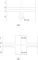
Fig. 2 is a schematic diagram of a solution for suppressing a narrow pulse; -
Fig. 3 is a schematic diagram of an example of a special interval; -
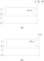
Fig. 4 is a schematic diagram of a Z0 interval output; -
Fig. 5 is a schematic diagram of a Z1 interval output; -
Fig. 6 is a schematic diagram of a Z2 interval output; -
Fig. 7 is a schematic diagram of a Z3 interval output; -
Fig. 8 is a schematic diagram of a Z4 interval output; -
Fig. 9 is a schematic diagram of a Z5 interval output; -
Fig. 10 is a schematic diagram of a Z6 interval output; -
Fig. 11 is a schematic diagram of a special state output. - The technical solutions in the examples of the present invention are clearly and completely described below with reference to the accompanying drawings in the examples of the present invention. Apparently, the described examples are some examples rather than all examples of the present invention. Based on the examples of the present invention, all other examples derived by those of ordinary skill in the art without making creative efforts fall within the scope of protection of the present invention.
- The present invention provides a technical solution as follows: a pulse width modulation (PWM) method for suppressing a narrow pulse. The method involves an interval confirmation module, a special state processing module, and a duty cycle output calculation module. As shown in
Fig. 1 , the method includes: a narrow pulse time DL and a dead time Dd in a duty cycle output are set based on a system design requirement and a system parameter, a duty cycle is divided into multiple interval segments to suppress a narrow pulse signal based on a relation between a duty cycle Dm and the narrow pulse time DL and a relation between a duty cycle Dm and the dead time Dd, and in an electric motor control system, a set duty cycle Dm obtained through a vector control calculation is input into the interval confirmation module; a dead time loss state is identified from a special jump state through the special state processing module, a finally-determined interval division value and a special jump state value are input into the duty cycle calculation module to calculate actual output duty cycles of upper and lower bridge arms of an insulated gate bipolar transistor (IGBT), and the actual output duty cycles are output to a driving module as an IGBT switching operation instruction; and an actual output duty cycle of the bridge arm of the IGBT is output in different forms on the basis of an interval where the actual output duty cycle is positioned based on an interval division result and a special interval result to obtain duty cycle outputs of different intervals for driving an IGBT module to be switched on or off. - Further, based on a system design, DL<Dd. The duty cycle is divided into 7 interval segments based on the relation between the duty cycle Dm and the narrow pulse time DL and the relation between a duty cycle Dm and the dead time Dd, and a voltage utilization rate is improved to a maximum extent, thereby realizing a duty cycle output effect shown in
Fig. 2 . In the electric motor control system, the set duty cycle Dm obtained through the vector control calculation is input into the interval confirmation module to determine an interval value, where an interval division form of the set duty cycle Dm is as follows: - a determination condition of a first interval Z0 is

- a determination condition of a second interval Z1 is

- a determination condition of a third interval Z2 is Dd ≤ Dm ≤ Dd + Dl ;
- a determination condition of a fourth interval Z3 is Dd + Dl ≤ Dm ≤ 1 - Dd - Dl ;
- a determination condition of a fifth interval Z4 is 1 - Dd - Dl ≤ Dm ≤ 1 - Dd ;
- a determination condition of a sixth interval Z5 is

- a determination condition of a seventh interval Z6 is

- Further, in the special state processing module, a dead time setting is added for a non-dead state occurring in a continuous state process, as shown in
Fig. 3 , and the state is defined as a special interval. - Further, the actual output duty cycle of the bridge arm of the IGBT is output in different forms on the basis of the interval where the actual output duty cycle is positioned based on the interval division result and the special interval result to obtain the duty cycle outputs of different intervals as follows for driving the IGBT module to be switched on or off:
- interval Z0: an actual output duty cycle of the upper bridge arm of the IGBT is Dt = 0, and a duty cycle output of the lower bridge arm is Db = 1, as shown in
Fig. 4 ; - interval Z1: an actual output duty cycle of the upper bridge arm of the IGBT is Dt = 0, and a duty cycle output of the lower bridge arm is Db = 1 - 2Dm , as shown in
Fig. 5 ; - interval Z2: an actual output duty cycle of the upper bridge arm of the IGBT is Dt = 0, and a duty cycle output of the lower bridge arm is Db = 1 - 2Dm , as shown in
Fig. 6 ; - interval Z3: an actual output duty cycle of the upper bridge arm of the IGBT is Dt = 0, and a duty cycle output of the lower bridge arm is Db = 1 - Dm - Dd , as shown in
Fig. 7 ; - interval Z4: an actual output duty cycle of the upper bridge arm of the IGBT is Dt = Dm - Dd , and a duty cycle output of the lower bridge arm is Db = 1 - Dm - Dd , as shown in
Fig. 8 ; - interval Z5: an actual output duty cycle of the upper bridge arm of the IGBT is Dt = Dm - Dd , and a duty cycle output of the lower bridge arm is Db = 0, as shown in
Fig. 9 ; - interval Z6: an actual output duty cycle of the upper bridge arm of the IGBT is Dt = 1, and a duty cycle output of the lower bridge arm is Db = 0, as shown in
Fig. 10 ; and - a special state: an actual output duty cycle of the upper bridge arm of the IGBT is Dt = 0, and a duty cycle output of the lower bridge arm is Db = 1 - 2Dm - Dd , as shown in
Fig. 11 . - While the examples of the present invention have been shown and described, it can be appreciated by those of ordinary skill in the art that various changes, modifications, substitutions, and variations can be made to these examples without departing from the principles and spirit of the present invention, and the scope of the present invention is defined by the appended claims and their equivalents.
Claims (4)
- A pulse width modulation (PWM) method for suppressing narrow pulses, comprising: an interval confirmation module, a special state processing module, and a duty cycle output calculation module, where the method comprises:setting a narrow pulse time period DL and a dead time period Dd in a duty cycle output based on a system configure requirement and a system parameter;dividing a duty cycle into a plurality of interval segments to suppress narrow pulses signal based on a relation between a duty cycle Dm and the narrow pulse time DL and a relation between the duty cycle Dm and the dead time period Dd, in an electric motor control system,inputting a duty cycle setting value Dm obtained through a vector control calculation into the interval confirmation module;identifying a dead time loss state from a special jump state through the special state processing module;inputting a finally-determined interval division value and a special jump state value into the duty cycle calculation module to calculate actual output duty cycle setting values of upper and lower bridge arms of an insulated gate bipolar transistor (IGBT) to output the actual output duty cycle setting values set as an IGBT switching operation instruction to a driving module; andoutputting an actual output duty cycle of the bridge arm of the IGBT in different forms on the basis of an interval where the actual output duty cycle is positioned based on an interval division result and a special interval result to obtain the duty cycle outputs of different intervals for driving an IGBT module to be switched on or off.
- The PWM method for suppressing narrow pulses as claimed in claim 1, wherein for a system design DL<Dd; and the duty cycle is divided into seven interval segments based on the relation between the duty cycle Dm and the narrow pulse time period DL and the relation between the duty cycle Dm and the dead time period Dd, in the electric motor control system, inputting the duty cycle setting value Dm obtained through the vector control calculation into the interval confirmation module, to determine an interval value, and an interval division form of the duty cycle setting value Dm is as follows:a determination condition of a first interval Z0 is
 a determination condition of a second interval Z1 is
 a determination condition of a third interval Z2 is Dd ≤ Dm ≤ Dd + Dl ;a determination condition of a fourth interval Z3 is Dd + Dl ≤ Dm ≤ 1 - Dd - Dl ;a determination condition of a fifth interval Z4 is 1 - Dd - Dl ≤ Dm ≤ 1 - Dd ;a determination condition of a sixth interval Z5 is
 a determination condition of a seventh interval Z6 is
- The PWM method for suppressing narrow pulses as claimed in claim 1, further comprising:in the special state processing module, adding a dead time setting for a non-dead state occurring in a continuous state process; anddetermining the non-dead state as a special interval.
- The PWM method for suppressing narrow pulses as claimed in claim 1 or 2, wherein the outputting the actual output duty cycle of the bridge arm of the IGBT in different forms on the basis of the interval where the actual output duty cycle is positioned based on the interval division result and the special interval result to obtain the duty cycle outputs of different intervals as follows for driving the IGBT module to be switched on or off:interval Z0: an actual output duty cycle value of the upper bridge arm of the IGBT is Dt = 0, and a duty cycle output of the lower bridge arm of the IGBT is Db = 1;interval Z1: an actual output duty cycle value of the upper bridge arm of the IGBT is Dt = 0, and a duty cycle output of the lower bridge arm of the IGBT is Db = 1 - 2Dm ,interval Z2: an actual output duty cycle value of the upper bridge arm of the IGBT is Dt = 0, and a duty cycle output of the lower bridge arm of the IGBT is Db = 1 - 2Dm ,interval Z3: an actual output duty cycle value of the upper bridge arm of the IGBT is Dt = 0, and a duty cycle output of the lower bridge arm of the IGBT is Db = 1 - Dm - Dd ;interval Z4: an actual output duty cycle value of the upper bridge arm of the IGBT is Dt = Dm - Dd , and a duty cycle output of the lower bridge arm of the IGBT is Db = 1 - Dm - Dd ;interval Z5: an actual output duty cycle value of the upper bridge arm of the IGBT is Dt = Dm - Dd , and a duty cycle output of the lower bridge arm of the IGBT is Db = 0;interval Z6: an actual output duty cycle value of the upper bridge arm of the IGBT is Dt = 1, and a duty cycle output of the lower bridge arm of the IGBT is Db = 0;a special state: an actual output duty cycle value of the upper bridge arm of the IGBT is Dt = 0, and a duty cycle output of the lower bridge arm of the IGBT is Db = 1 - 2Dm - Dd.
Applications Claiming Priority (2)
| Application Number | Priority Date | Filing Date | Title |
|---|---|---|---|
| CN202110370310.2A CN113270996B (en) | 2021-04-07 | 2021-04-07 | PWM modulation method for restraining narrow pulse |
| PCT/CN2021/133007 WO2022213618A1 (en) | 2021-04-07 | 2021-11-25 | Pwm method for suppressing narrow pulses |
Publications (2)
| Publication Number | Publication Date |
|---|---|
| EP4270749A1 true EP4270749A1 (en) | 2023-11-01 |
| EP4270749A4 EP4270749A4 (en) | 2024-06-26 |
Family
ID=77228521
Family Applications (1)
| Application Number | Title | Priority Date | Filing Date |
|---|---|---|---|
| EP21935835.5A Pending EP4270749A4 (en) | 2021-04-07 | 2021-11-25 | MID PROCESS FOR SUPPRESSING NARROW PULSES |
Country Status (3)
| Country | Link |
|---|---|
| EP (1) | EP4270749A4 (en) |
| CN (1) | CN113270996B (en) |
| WO (1) | WO2022213618A1 (en) |
Families Citing this family (5)
| Publication number | Priority date | Publication date | Assignee | Title |
|---|---|---|---|---|
| CN113270996B (en) * | 2021-04-07 | 2022-11-11 | 中国第一汽车股份有限公司 | PWM modulation method for restraining narrow pulse |
| CN113938361B (en) * | 2021-09-03 | 2024-04-16 | 广东安朴电力技术有限公司 | Communication coding anti-interference method, system and storage medium |
| CN114977972B (en) * | 2022-06-23 | 2025-09-09 | 中国第一汽车股份有限公司 | Motor control method and device and vehicle |
| CN115065295B (en) * | 2022-06-30 | 2026-06-30 | 中国第一汽车股份有限公司 | Motor control method, motor controller, electric drive system and new energy automobile |
| CN116073804B (en) * | 2022-11-15 | 2025-12-05 | 中国第一汽车股份有限公司 | A method and apparatus for generating PWM waveforms |
Family Cites Families (20)
| Publication number | Priority date | Publication date | Assignee | Title |
|---|---|---|---|---|
| JPH09285133A (en) * | 1996-04-12 | 1997-10-31 | Fuji Electric Co Ltd | Control device for power converter |
| US6714424B2 (en) * | 2001-11-30 | 2004-03-30 | Ballard Power Systems Corporation | Dead-time compensation with narrow pulse elimination in solid- state switch devices |
| JP2005094944A (en) * | 2003-09-18 | 2005-04-07 | Matsushita Electric Ind Co Ltd | Brushless motor |
| US8648561B2 (en) * | 2007-03-27 | 2014-02-11 | Danfoss Drives A/S | Method for driving a pulse width modulated controller |
| WO2012008164A1 (en) * | 2010-07-16 | 2012-01-19 | パナソニック株式会社 | Noise elimination device, noise elimination method and vehicle in-built display device using same noise elimination device |
| JP6019770B2 (en) * | 2012-06-01 | 2016-11-02 | 株式会社明電舎 | Bidirectional insulation type DC-DC converter control device |
| CN103715956B (en) * | 2013-12-16 | 2015-12-02 | 华南理工大学 | A kind of two level three-phase space vector pulse-width modulation and SVPWM optimization method thereof |
| US9882500B2 (en) * | 2014-12-07 | 2018-01-30 | Alpha & Omega Semiconductor (Cayman), Ltd. | Power supply device |
| CN105305799A (en) * | 2015-11-13 | 2016-02-03 | 四川长虹电器股份有限公司 | Narrow pulse limit control method for variable frequency controller |
| CN106100393B (en) * | 2016-07-14 | 2018-11-20 | 中车大连电力牵引研发中心有限公司 | Single-phase four-quadrant rectifier dead-zone compensation method and device |
| CN107453641A (en) * | 2017-08-30 | 2017-12-08 | 汪明生 | A kind of two level two-phase space vector pulse width modulation devices and its SVPWM methods |
| JP2020028158A (en) * | 2018-08-10 | 2020-02-20 | 住友重機械工業株式会社 | Control device for power converter |
| CN110875709B (en) * | 2018-08-30 | 2021-10-22 | 比亚迪股份有限公司 | Inverter protection method and system and vehicle |
| CN109412442B (en) * | 2018-10-31 | 2020-05-19 | 华中科技大学 | A Zero Common Mode Modulation Method for MMC |
| CN210111841U (en) * | 2018-12-14 | 2020-02-21 | 特变电工西安电气科技有限公司 | Three-level inverter narrow pulse suppression device |
| CN110323927B (en) * | 2018-12-14 | 2024-06-14 | 特变电工西安电气科技有限公司 | A method and device for suppressing narrow pulses of three-level inverter |
| CN110557040B (en) * | 2019-09-06 | 2021-07-06 | 武汉理工通宇新源动力有限公司 | Method, device and system for eliminating narrow pulse in two-level SVPWM (space vector pulse width modulation) and inverter |
| CN111478613B (en) * | 2020-04-20 | 2021-07-27 | 上海正泰电源系统有限公司 | DSP implementation method for restraining inverter narrow pulse |
| CN112510978B (en) * | 2020-11-24 | 2021-09-17 | 廊坊英博电气有限公司 | Method, device, equipment and storage medium for suppressing driving narrow pulse |
| CN113270996B (en) * | 2021-04-07 | 2022-11-11 | 中国第一汽车股份有限公司 | PWM modulation method for restraining narrow pulse |
-
2021
- 2021-04-07 CN CN202110370310.2A patent/CN113270996B/en active Active
- 2021-11-25 EP EP21935835.5A patent/EP4270749A4/en active Pending
- 2021-11-25 WO PCT/CN2021/133007 patent/WO2022213618A1/en not_active Ceased
Also Published As
| Publication number | Publication date |
|---|---|
| EP4270749A4 (en) | 2024-06-26 |
| CN113270996A (en) | 2021-08-17 |
| WO2022213618A1 (en) | 2022-10-13 |
| CN113270996B (en) | 2022-11-11 |
Similar Documents
| Publication | Publication Date | Title |
|---|---|---|
| CN113270996B (en) | PWM modulation method for restraining narrow pulse | |
| CN102611348B (en) | PWM output method to solve uneven heat generation of bridge arm switches in single-phase full-bridge inverter circuit | |
| CN106411210B (en) | Control device of electric motor, rote learning devices and methods therefor | |
| CN102237838B (en) | Braking current control method and device for electric bicycle controller | |
| CN110707988B (en) | Specific harmonic elimination pulse width modulation control system | |
| EP3232555A1 (en) | Sub-module distributed control method, device and system | |
| CN105186887A (en) | Switching device temperature based cascaded high-voltage variable frequency dynamic switching frequency PWM (pulse width modulation) adjustment method | |
| CN106655953B (en) | Electrolytic capacitor-free motor drive system and its field weakening control method and control device | |
| CN110829920A (en) | Modulation device and system | |
| CN114624588A (en) | Servo motor operation supervisory systems based on data analysis | |
| CN111585487B (en) | System for controlling motor to sound | |
| CN110661406B (en) | Minimum current harmonic pulse width modulation system based on stator flux linkage | |
| CN115263252B (en) | Intermittent pumping control method and system for oil pumping unit | |
| CN107453641A (en) | A kind of two level two-phase space vector pulse width modulation devices and its SVPWM methods | |
| CN117792208A (en) | Robot module transmission speed cooperative work control system and method | |
| WO2023246484A1 (en) | Electric motor control method and apparatus, and vehicle | |
| CN104896961B (en) | The power coordination control device of multiple electric furnace operations | |
| CN114465225A (en) | Intelligent peak shift operation control method and device for multi-well common DC bus group control of pumping units | |
| CN106357093A (en) | Method and system for improving current sampling precision | |
| CN113922720A (en) | A PMSM Model Predictive Current Control Algorithm Based on Duty Cycle Control | |
| CN116865630B (en) | Motor variable-frequency speed regulation control system | |
| CN108390553B (en) | Compensation method for motor transmission PWM dead zone | |
| CN215378798U (en) | A lithium battery adaptive DC brushless motor driver | |
| CN116147370B (en) | Control methods and related devices for AC electric arc furnace smelting equipment | |
| CN117767836B (en) | Centralized control method and system for motor operation |
Legal Events
| Date | Code | Title | Description |
|---|---|---|---|
| STAA | Information on the status of an ep patent application or granted ep patent |
Free format text: STATUS: THE INTERNATIONAL PUBLICATION HAS BEEN MADE |
|
| PUAI | Public reference made under article 153(3) epc to a published international application that has entered the european phase |
Free format text: ORIGINAL CODE: 0009012 |
|
| STAA | Information on the status of an ep patent application or granted ep patent |
Free format text: STATUS: REQUEST FOR EXAMINATION WAS MADE |
|
| 17P | Request for examination filed |
Effective date: 20230728 |
|
| AK | Designated contracting states |
Kind code of ref document: A1 Designated state(s): AL AT BE BG CH CY CZ DE DK EE ES FI FR GB GR HR HU IE IS IT LI LT LU LV MC MK MT NL NO PL PT RO RS SE SI SK SM TR |
|
| REG | Reference to a national code |
Ref country code: DE Ref legal event code: R079 Free format text: PREVIOUS MAIN CLASS: H02M0001080000 Ipc: H02M0007539500 |
|
| A4 | Supplementary search report drawn up and despatched |
Effective date: 20240527 |
|
| RIC1 | Information provided on ipc code assigned before grant |
Ipc: H02P 27/08 20060101ALI20240521BHEP Ipc: H02M 1/00 20060101ALI20240521BHEP Ipc: H02M 1/08 20060101ALI20240521BHEP Ipc: H02M 7/5395 20060101AFI20240521BHEP |
|
| DAV | Request for validation of the european patent (deleted) | ||
| DAX | Request for extension of the european patent (deleted) | ||
| STAA | Information on the status of an ep patent application or granted ep patent |
Free format text: STATUS: EXAMINATION IS IN PROGRESS |
|
| 17Q | First examination report despatched |
Effective date: 20251008 |