EP4270643A1 - Electronic device capable of improving antenna performance - Google Patents
Electronic device capable of improving antenna performance Download PDFInfo
- Publication number
- EP4270643A1 EP4270643A1 EP21913589.4A EP21913589A EP4270643A1 EP 4270643 A1 EP4270643 A1 EP 4270643A1 EP 21913589 A EP21913589 A EP 21913589A EP 4270643 A1 EP4270643 A1 EP 4270643A1
- Authority
- EP
- European Patent Office
- Prior art keywords
- matching
- capacitor
- antenna body
- inductor
- electronic device
- Prior art date
- Legal status (The legal status is an assumption and is not a legal conclusion. Google has not performed a legal analysis and makes no representation as to the accuracy of the status listed.)
- Withdrawn
Links
- 239000002184 metal Substances 0.000 claims abstract description 34
- 239000003990 capacitor Substances 0.000 claims description 76
- 238000001914 filtration Methods 0.000 claims description 7
- 238000010295 mobile communication Methods 0.000 claims description 4
- 238000005516 engineering process Methods 0.000 claims description 3
- 102100032533 ADP/ATP translocase 1 Human genes 0.000 description 47
- 101000768061 Escherichia phage P1 Antirepressor protein 1 Proteins 0.000 description 47
- 101000796932 Homo sapiens ADP/ATP translocase 1 Proteins 0.000 description 47
- 102100026396 ADP/ATP translocase 2 Human genes 0.000 description 39
- 101000718417 Homo sapiens ADP/ATP translocase 2 Proteins 0.000 description 39
- 238000010586 diagram Methods 0.000 description 15
- 230000006870 function Effects 0.000 description 7
- 230000005855 radiation Effects 0.000 description 5
- 230000005684 electric field Effects 0.000 description 3
- 230000008859 change Effects 0.000 description 2
- 230000005284 excitation Effects 0.000 description 2
- 230000006872 improvement Effects 0.000 description 2
- 230000004044 response Effects 0.000 description 2
- 230000009471 action Effects 0.000 description 1
- 238000004891 communication Methods 0.000 description 1
- 230000000694 effects Effects 0.000 description 1
- 239000011521 glass Substances 0.000 description 1
- 238000002955 isolation Methods 0.000 description 1
- 239000000463 material Substances 0.000 description 1
- 238000000034 method Methods 0.000 description 1
- 230000002093 peripheral effect Effects 0.000 description 1
- 239000011347 resin Substances 0.000 description 1
- 229920005989 resin Polymers 0.000 description 1
Images




Classifications
-
- H—ELECTRICITY
- H01—ELECTRIC ELEMENTS
- H01Q—ANTENNAS, i.e. RADIO AERIALS
- H01Q1/00—Details of, or arrangements associated with, antennas
- H01Q1/44—Details of, or arrangements associated with, antennas using equipment having another main function to serve additionally as an antenna, e.g. means for giving an antenna an aesthetic aspect
-
- H—ELECTRICITY
- H01—ELECTRIC ELEMENTS
- H01Q—ANTENNAS, i.e. RADIO AERIALS
- H01Q1/00—Details of, or arrangements associated with, antennas
- H01Q1/12—Supports; Mounting means
- H01Q1/22—Supports; Mounting means by structural association with other equipment or articles
-
- H—ELECTRICITY
- H01—ELECTRIC ELEMENTS
- H01Q—ANTENNAS, i.e. RADIO AERIALS
- H01Q1/00—Details of, or arrangements associated with, antennas
- H01Q1/36—Structural form of radiating elements, e.g. cone, spiral, umbrella; Particular materials used therewith
-
- H—ELECTRICITY
- H01—ELECTRIC ELEMENTS
- H01Q—ANTENNAS, i.e. RADIO AERIALS
- H01Q1/00—Details of, or arrangements associated with, antennas
- H01Q1/48—Earthing means; Earth screens; Counterpoises
-
- H—ELECTRICITY
- H01—ELECTRIC ELEMENTS
- H01Q—ANTENNAS, i.e. RADIO AERIALS
- H01Q1/00—Details of, or arrangements associated with, antennas
- H01Q1/50—Structural association of antennas with earthing switches, lead-in devices or lightning protectors
-
- H—ELECTRICITY
- H01—ELECTRIC ELEMENTS
- H01Q—ANTENNAS, i.e. RADIO AERIALS
- H01Q21/00—Antenna arrays or systems
- H01Q21/0006—Particular feeding systems
-
- H—ELECTRICITY
- H01—ELECTRIC ELEMENTS
- H01Q—ANTENNAS, i.e. RADIO AERIALS
- H01Q21/00—Antenna arrays or systems
- H01Q21/28—Combinations of substantially independent non-interacting antenna units or systems
-
- H—ELECTRICITY
- H01—ELECTRIC ELEMENTS
- H01Q—ANTENNAS, i.e. RADIO AERIALS
- H01Q21/00—Antenna arrays or systems
- H01Q21/30—Combinations of separate antenna units operating in different wavebands and connected to a common feeder system
-
- H—ELECTRICITY
- H01—ELECTRIC ELEMENTS
- H01Q—ANTENNAS, i.e. RADIO AERIALS
- H01Q5/00—Arrangements for simultaneous operation of antennas on two or more different wavebands, e.g. dual-band or multi-band arrangements
- H01Q5/20—Arrangements for simultaneous operation of antennas on two or more different wavebands, e.g. dual-band or multi-band arrangements characterised by the operating wavebands
-
- H—ELECTRICITY
- H01—ELECTRIC ELEMENTS
- H01Q—ANTENNAS, i.e. RADIO AERIALS
- H01Q5/00—Arrangements for simultaneous operation of antennas on two or more different wavebands, e.g. dual-band or multi-band arrangements
- H01Q5/30—Arrangements for providing operation on different wavebands
- H01Q5/307—Individual or coupled radiating elements, each element being fed in an unspecified way
- H01Q5/314—Individual or coupled radiating elements, each element being fed in an unspecified way using frequency dependent circuits or components, e.g. trap circuits or capacitors
- H01Q5/328—Individual or coupled radiating elements, each element being fed in an unspecified way using frequency dependent circuits or components, e.g. trap circuits or capacitors between a radiating element and ground
-
- H—ELECTRICITY
- H01—ELECTRIC ELEMENTS
- H01Q—ANTENNAS, i.e. RADIO AERIALS
- H01Q5/00—Arrangements for simultaneous operation of antennas on two or more different wavebands, e.g. dual-band or multi-band arrangements
- H01Q5/30—Arrangements for providing operation on different wavebands
- H01Q5/307—Individual or coupled radiating elements, each element being fed in an unspecified way
- H01Q5/314—Individual or coupled radiating elements, each element being fed in an unspecified way using frequency dependent circuits or components, e.g. trap circuits or capacitors
- H01Q5/335—Individual or coupled radiating elements, each element being fed in an unspecified way using frequency dependent circuits or components, e.g. trap circuits or capacitors at the feed, e.g. for impedance matching
-
- H—ELECTRICITY
- H01—ELECTRIC ELEMENTS
- H01Q—ANTENNAS, i.e. RADIO AERIALS
- H01Q5/00—Arrangements for simultaneous operation of antennas on two or more different wavebands, e.g. dual-band or multi-band arrangements
- H01Q5/30—Arrangements for providing operation on different wavebands
- H01Q5/307—Individual or coupled radiating elements, each element being fed in an unspecified way
- H01Q5/342—Individual or coupled radiating elements, each element being fed in an unspecified way for different propagation modes
- H01Q5/357—Individual or coupled radiating elements, each element being fed in an unspecified way for different propagation modes using a single feed point
- H01Q5/364—Creating multiple current paths
-
- H—ELECTRICITY
- H01—ELECTRIC ELEMENTS
- H01Q—ANTENNAS, i.e. RADIO AERIALS
- H01Q5/00—Arrangements for simultaneous operation of antennas on two or more different wavebands, e.g. dual-band or multi-band arrangements
- H01Q5/50—Feeding or matching arrangements for broad-band or multi-band operation
-
- H—ELECTRICITY
- H01—ELECTRIC ELEMENTS
- H01Q—ANTENNAS, i.e. RADIO AERIALS
- H01Q9/00—Electrically-short antennas having dimensions not more than twice the operating wavelength and consisting of conductive active radiating elements
- H01Q9/04—Resonant antennas
- H01Q9/30—Resonant antennas with feed to end of elongated active element, e.g. unipole
- H01Q9/42—Resonant antennas with feed to end of elongated active element, e.g. unipole with folded element, the folded parts being spaced apart a small fraction of the operating wavelength
Definitions
- the present disclosure relates to mobile communication technology, and particularly, to an electronic device capable of improving performance of an antenna.
- Embodiments of the present disclosure provide an electronic device capable of improving performance of an antenna to solve the above problems.
- an electronic device capable of improving performance of an antenna.
- the electronic device includes a metal frame.
- the metal frame has at least one gap.
- the at least one gap divides the metal frame into at least one frame section.
- the at least one frame section is used as antenna bodies and supporting corresponding frequency bands.
- the at least one frame section at least forms a first antenna body supporting a middle high band (MHB) and a second antenna body supporting a low band (LB).
- the first antenna body and the second antenna body are disposed adjacent to each other and isolated by means of the at least one gap.
- the first antenna body is further integrated with a transceiving function of at least one high band (HB) to support the MHB and the at least one HB.
- HB high band
- the metal frame can support the at least one HB, and the performance of an antenna is improved. Moreover, it is not required to provide antenna bodies supporting the HB in the electronic device, such that the cost is reduced. In addition, no matter whether a rear cover is a metal rear cover or a rear cover printed with a circuit board, the performance of antenna frequency bands such as the HB may not be affected.
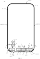
- FIG. 1 is a schematic plan view illustrating a part of an internal structure of an electronic device 100 capable of improving performance of an antenna (hereinafter referred to as: electronic device) according to an embodiment of the present disclosure.
- the electronic device 100 includes a metal frame 10.
- the metal frame 10 has at least one gap 11.
- the at least one gap 11 divides the metal frame 10 into at least one frame section 12, and the at least one frame section 12 is used as antenna bodies and supports corresponding frequency bands.
- the at least one frame section 12 at least forms a first antenna body ANT1 supporting a middle high band (MHB) and a second antenna body ANT2 supporting a low band (LB).
- MHB middle high band
- LB low band
- the first antenna body ANT1 and the second antenna body ANT2 are disposed adjacent to each other and isolated by means of the gap 11.
- the first antenna body ANT1 is further integrated with a transceiving function of at least one high band (HB) to support the MHB and the at least one HB, i.e., supporting transceiving of radio-frequency signals of the MHB and the at least one HB.
- HB high band
- antenna bodies supporting the HB in the related art are generally disposed inside the electronic device 100 to minimize the influence on performance of an antenna.
- the metal frame 10 can implement the supporting for the at least one HB, and the performance of an antenna is improved.
- a rear cover of the electronic device 100 is a metal rear cover or a rear cover printed with a circuit board or a rear cover with an electrochromic function, the transceiving performance of antenna frequency bands such as the HB may not be affected.
- the electronic device 100 further includes an MHB feed source S1, at least one HB feed source S2, and a combiner 13.
- the combiner 13 is connected among the MHB feed source S1, the at least one HB feed source S2, and the first antenna body ANT1, and the combiner 13 is configured to combine feed signals provided by the MHB feed source S 1 and the at least one HB feed source S2 and provide the feed signals to the first antenna body ANT1, enabling the first antenna body ANT1 to support the MHB and the at least one HB.
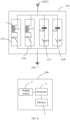
- the combiner 13 is an all-in-one combiner.
- the combiner 13 includes a first input end 131, at least one second input end 132, and an output end 133.
- the first input end 131 is configured to be connected to the MHB feed source S1.
- the at least one second input end 132 is configured to be connected to the at least one HB feed source S2, respectively.
- the output end 133 is configured to be connected to the first antenna body ANT1.
- the MHB feed source S1 provides a feed signal of the MHB
- the at least one HB feed source S2 provides a feed signal of the at least one HB.
- the combiner 13 is configured to combine the feed signal of the MHB provided by the MHB feed source S1 and received by the first input end 131 with the feed signal of the at least one HB provided by the at least one HB feed source S2 and received by the at least one second input end 132, and then provide the combined feed signals to the first antenna body ANT1, enabling the first antenna body ANT1 to support the MHB and the at least one HB.
- the antenna device 100 further includes a first matching circuit 14.
- the first matching circuit 14 is connected between the combiner 13 and the first antenna body ANT1 and configured to implement impedance matching of the MHB and the at least one HB.
- the first antenna body ANT1 includes a feed point F1.
- the above expression "the combiner 13 is connected among the MHB feed source S1, the at least one HB feed source S2, and the first antenna body ANT1" indicates that the combiner 13 is connected among the MHB feed source S1, the at least one HB feed source S2, and the feed point F1 of the first antenna body ANT1.
- the output end 133 being configured to be connected to the first antenna body ANT1 indicates that the output end 133 is configured to be connected to the feed point F1 of the first antenna body ANT1.
- the first matching circuit 14 being connected between the combiner 13 and the first antenna body ANT1 also indicates that the first matching circuit 14 is connected between the combiner 13 and the feed point F1 of the first antenna body ANT1.
- the first matching circuit 14 is specifically connected between the output end 133 of the combiner 13 and the feed point F1 of the first antenna body ANT1.
- the HB may be effectively excited, and the radiation performance of the HB is improved.
- the MHB is a frequency band in a range from 1710 MHz to 2690 MHz.
- the at least one HB is a frequency band other than the MHB, for example, a frequency band of 3000 MHZ or above.
- the at least one HB includes a 5th Generation Mobile Communication Technology (5G) N78 frequency band and a 5G N79 frequency band
- the at least one HB feed source S2 includes a feed source for generating feed signals of the 5GN78 frequency band and the 5G N79 frequency band.
- the 5G N78 frequency band and the 5G N79 frequency band are an N78 frequency band and an N79 frequency band under the 5G NSA communication standard, respectively.
- the 5GN78 frequency band ranges from 3400 MHZ to 3600 MHZ
- the 5G N79 frequency band ranges from 4800 MHZ to 5000 MHZ.
- the first matching circuit 14 performs matching adjustment, at least to excite the resonance of the N79 frequency band, thereby achieving effective excitation of the N79 frequency band.
- the resonance of the MHB, the 5G N78 frequency band and the 5G N79 frequency band may be effectively excited through impedance matching adjustment performed by the first matching circuit 14. That is, the first antenna body ANT1 may achieve better resonance in the MHB, the 5G N78 frequency band and the 5G N79 frequency band, thereby reducing loss and improving radiation performance.
- FIG. 3 is a schematic structural diagram of the first matching circuit 14 according to an embodiment of the present disclosure.
- the first matching circuit 14 includes a first inductor L1, a first capacitor C1, and a second capacitor C2.
- the first inductor L1 and the first capacitor C1 are sequentially connected in series between the combiner 13 and the first antenna body ANT1, that is, they are sequentially connected in series between the combiner 13 and the feed point F1 of the first antenna body ANT1.
- the second capacitor C2 is connected between the ground and a connection node N1 of the first inductor L1 and the first capacitor C1.
- the first inductor L1 has an inductance value of 3.3 NH (nanohenry, namely, 10 -9 henry), the first capacitor C1 has a capacitance value of 1 PF (picofarad, namely 10 -12 farad), and the second capacitor C2 has a capacitance value of 0.5 PF.
- the HB can be effectively excited, and the radiation performance of the HB is improved.
- the first inductor L1 and the second capacitor C2 constitute a structure for exciting a resonance of the first antenna body ANT1 in the 5G N79 frequency band, thereby implementing effective excitation of the 5G N79 frequency band. In this way, the first antenna body ANT1 can implement better radiation performance in the 5GN79 frequency band.
- the at least one HB may also include a WIFI 5G frequency band, and the first antenna body ANT1 also supports transceiving of radio-frequency signals in the WIFI 5G frequency band. That is, in some embodiments, the at least one HB feed source S2 of the electronic device 100 further includes a feed source for generating a feed signal of the WIFI 5G frequency band.
- the combiner 13 may further combine the feed signal of the WIFI 5G frequency band with the feed signal of the MHB and the feed signals of the 5G N78 frequency band and the 5G N79 frequency band to obtain combined feed signals, and the first matching circuit 14 performs matching and tuning, enabling the first antenna body ANT1 to simultaneously support the MHB, the 5G N78 frequency band, the 5G N79 frequency band, and the WIFI 5G frequency band.
- the WIFI 5G frequency band ranges from 5.15 to 5.85 MHz.
- the electronic device 100 further includes a second matching circuit 15 and an LB feed source S3.
- the second matching circuit 15 is connected between the LB feed source S3 and the second antenna body ANT2, and the second matching circuit is configured to implement impedance matching of the LB and filter matching for filtering away the MHB and the HB, thereby isolating the first antenna body ANT1 from the second antenna body ANT1.
- signals of the MHB and signals of the HB such as the 5G N78 frequency band, the 5G N79 frequency band and the WIFI 5G frequency band are filtered away on the second antenna body ANT2 by means of the second matching circuit 15. Therefore, no signal interference may occur even if the first antenna body ANT1 and the second antenna body ANT2 are disposed adjacent to each other, thereby implementing isolation of the first antenna body ANT1 from the second antenna body ANT1.
- FIG. 4 is a schematic structural diagram of the second matching circuit 15 according to an embodiment of the present disclosure.
- the second matching circuit 15 includes a second inductor L2, a third inductor L3, and a third capacitor C3.
- the second inductor L2 is connected between the LB feed source S3 and the second antenna body ANT2.
- the third inductor L3 and the third capacitor C3 are connected in parallel between the ground and a connection node N2 of the second inductor L2 and the second antenna body ANT2.
- the second antenna body ANT2 includes a feed point F2.
- the second matching circuit 15 being connected between the LB feed source S3 and the second antenna body ANT2 indicates that the second matching circuit 15 is connected between the LB feed source S3 and the feed point F2 of the second antenna body ANT2.
- the second inductor L2 being connected between the LB feed source S3 and the second antenna body ANT2 also indicates that the second inductor L2 is connected between the LB feed source S3 and the feed point F2 of the second antenna body ANT2.
- the connection node N2 of the second inductor L2 and the second antenna body ANT2 also refers to the connection node N2 between the second inductor L2 and the feed point F2 of the second antenna body ANT2.
- the second inductor has an inductance value of 3.3 NH
- the third inductor has an inductance value of 15 NH
- the third capacitor has a capacitance value of 5 PF.
- the impedance matching of the LB may be implemented, and meanwhile, the filter matching for filtering away the MHB and the HB is also implemented, thereby isolating the first antenna body ANT1 from the second antenna body ANT2.
- the parallel structure between the third inductor L3 and the third capacitor C3 constitutes a filtering circuit for filtering away the MHB and the HB, that is, the second matching circuit 15 implements the filtering effect of filtering away the middle high band through the parallel structure between the third inductor L3 and the third capacitor C3.
- the electronic device 100 further includes at least one switch unit 16.
- the at least one switch unit 16 is connected between a target position of the second antenna body ANT2 and the ground.
- the target position is a position between the feed point F2 of the second antenna body ANT2 and an end D1, close to the first antenna body ANT1, of the second antenna body ANT2.
- the above-mentioned feed point F2 of the second antenna body ANT2 is a connection point/signal feed point connected to the second matching circuit.
- the target position may be any position between the feed point F2 of the second antenna body ANT2 and the end D1, close to the first antenna body ANT1, of the second antenna body ANT2.
- FIG. 5 is a schematic structural diagram of the switch unit 16 according to an embodiment of the present disclosure.
- each of the at least one switch unit 16 includes a plurality of matching element branches Z1 connected in parallel, and each matching element branch includes a matching element M1 and a switch SW1 that are connected in series.
- the matching elements M1 in different matching element branches Z1 are different in terms of at least one of types and parameters.
- Different matching element branches are selected to operate by controlling on/off of the switches in the different matching element branches, such that the first antenna body ANT1 and the second antenna body ANT2 can support transceiving of radio-frequency signals in different frequency bands, thereby extending the frequency band range of the first antenna body and the second antenna body.
- the first antenna body ANT1 and the second antenna body ANT2 are disposed adjacent to each other and isolated by means of the gap 11.
- the first antenna body ANT1 and the second antenna body ANT2 are antennas with a common aperture/gap.
- the first antenna body ANT1 may also be coupled to the second antenna body ANT2 through the gap 11, and is grounded through the at least one switch unit 16, thereby forming a feed path passing through the gap 11 and the at least one switch unit 16.
- the second antenna body ANT2 may also form a feed path from the feed point F2 of the second antenna body ANT2 to the at least one switch unit 16 and then to the ground.
- resonance frequencies of the first antenna body ANT1 and the second antenna body ANT2 may be affected at the same time, so as to change the frequency bands supported by the first antenna body ANT1 and the second antenna body ANT2.
- the first antenna body ANT1 and the second antenna body ANT2 may operate in different frequency bands according to needs, thereby extending bandwidths of the first antenna body ANT1 and the second antenna body ANT2.
- FIG. 6 is a schematic structural diagram of a first switch unit according to an embodiment of the present disclosure.
- the at least one switch unit 16 includes the first switch unit 161, and the target position includes a first target position P1.
- the first switch unit 161 includes a first inductor matching branch Z11, a first capacitor matching branch Z12, a second capacitor matching branch Z13, and a third capacitor matching branch Z14, which are connected in parallel between the first target position P1 and the ground.
- the first inductor matching branch Z11 includes a first matching inductor L11 and a switch SW1 that are connected in series.
- the first capacitor matching branch Z12 includes a first matching capacitor C11 and a switch SW1 that are connected in series.
- the second capacitor matching branch Z13 includes a second matching capacitor C12 and a switch SW1 that are connected in series.
- the third capacitor matching branch Z14 includes a third matching capacitor C13 and a switch SW1 that are connected in series.
- the first matching capacitor C11, the second matching capacitor C12, and the third matching capacitor C13 have different capacitance values.
- the first inductor matching branch Z11, the first capacitor matching branch Z12, the second capacitor matching branch Z13 and the third capacitor matching branch Z14 are different in terms of types or parameters, when different matching branches are switched on or different combinations of matching branches are switched on, different matching parameters are generated, thereby implementing resonance matching of different frequency bands.
- the first matching inductor has an inductance value of 12 NH
- the first matching capacitor has a capacitance value of 0.5 PF
- the second matching capacitor has a capacitance value of 1.2 PF
- the third matching capacitor has a capacitance value of 3 PF.
- FIG. 7 is a schematic structural diagram of a second switch unit 162 according to an embodiment of the present disclosure. As illustrated in FIG. 1 and FIG. 7 , the at least one switch unit 16 further includes a second switch unit 162, and the target position further includes a second target position P2 located between the first target position P1 and the feed point F2 of the second antenna body ANT2.
- the second switch unit 162 includes a second inductor matching branch Z15, a third inductor matching branch Z16, a fourth capacitor matching branch Z17, and a fifth capacitor matching branch Z18, which are connected in parallel between the second target position P2 and the ground.
- the second inductor matching branch Z15 includes a second matching inductor L12 and a switch SW1 that are connected in series.
- the third inductor matching branch Z16 includes a third matching inductor L13 and a switch S21 that are connected in series.
- the fourth capacitor matching branch Z17 includes a fourth matching capacitor C14 and a switch SW1 that are connected in series.
- the fifth capacitor matching branch Z18 includes a fifth matching capacitor C15 and a switch SW1 that are connected in series.
- the second matching inductor L12 and the third matching inductor L13 have different inductance values, and the fourth matching capacitor C14 and the fifth matching capacitor C15 have different capacitance values.
- the second matching inductor L12 has an inductance value of 24 NH
- the third matching inductor L13 has an inductance value of 15 NH
- the fourth matching capacitor C14 has a capacitance value of 0.3 PF
- the fifth matching capacitor C15 has a capacitance value of 3 PF.
- the switches SW1 in the at least one switch unit 16 are computer numerical control switches, for example, MOS transistors, BJT triode, etc.
- FIG. 8 is a functional module diagram of the electronic device 100.
- the electronic device 100 may further include a processor 2, a memory 3, and a display screen 4.
- the memory 3 may store corresponding relationships between a switch control logic in the switch unit and the frequency bands supported by the first antenna body ANT0 and the second antenna body ANT2.
- the processor 2 can determine a frequency band covered by a target network to be switched to in response to a network switching operation, for example, in response to a user's operation performed via menu options, icons, etc. displayed on the display screen 4 for controlling switching from a 4G network to a 5G network, or from a mobile communication network to a WIFI network, etc.
- a corresponding switch control logic can be obtained based on the corresponding relationships between the switch control logic in the at least one switch unit and the frequency bands supported by the first antenna body ANT0 and the second antenna body ANT2 stored in the memory 3 in advance, so as to control the plurality of switches SW1 in the at least one switch unit 16 to be switched on or off correspondingly.
- the switch unit 16 can be adjusted to corresponding matching parameters, and the first antenna body ANT0 and the second antenna body ANT2 currently operate in the frequency band covered by the target network to support transceiving of radio-frequency signals in the frequency band covered by the target network.
- the processor 2 may include a plurality of output controlling terminals that may be connected to controlled terminals of all the switches SW1 of the at least one switch unit 16 in one-to-one correspondence.
- the switches SW1 in the at least one switch unit 16 are MOS transistors
- the plurality of output controlling terminals of the processor 2 may be connected to gates of all MOS transistors of the at least one switch unit 16, respectively.
- the switch control logic defines a level outputted by each of the output controlling terminals of the processor.
- the processor 2 can control each of the output controlling terminals to output a signal of the corresponding level to the controlled terminal of the corresponding switch SW1 in the at least one switch unit 16 based on the corresponding switch control logic, thereby controlling the plurality of switches SW1 in the at least one switch unit 16 to be correspondingly switched on or off.
- the metal frame 10 is a peripheral frame of the electronic device 100, and may be used as antenna bodies for transceiving of radio-frequency signals.
- the electronic device 100 is roughly in a form of square
- the metal frame 10 is a rectangular frame and includes two short frames 101 opposite to each other and two long frames 102 opposite to each other.
- the metal frame 10 is defined by the two short frames 101 opposite to each other and the two long frames 102 opposite to each other.
- the two short frames 101 include a first short frame 101a and a second short frame 101b.
- the two long frames 102 include a first long frame 102a and a second long frame 102b.
- the first short frame 101a is located at a bottom of the electronic device 100.
- the second short frame 101b is located at a top of the electronic device 100.
- the first long frame 102a is located on a left side of the electronic device 100.
- the second long frame 102b is located on a right side of the electronic device 100.
- the metal frame 10 is provided with at least one gap 11, and the at least one gap 11 at least includes a first gap 11a defined in the first short frame 101a.
- a certain position on the first long frame 102a is grounded to define a first grounding point G1.
- a certain position on the second long frame 102b is grounded to define a second grounding point G2.
- the second antenna body ANT1 is formed by a frame portion between the first gap 11 and the first grounding point G1.
- the second antenna body ANT2 is formed by a frame portion between the first gap 11 and the second grounding point G2.
- the certain position which is grounded to define the first grounding point G1 in the first long frame 102a, may be a position on the first long frame 102a close to the first short frame 101b.
- the certain position, which is grounded to define the first grounding point G2 in the second long frame 102b, may also be a position on the second long frame 102b close to the first short frame 101b.
- FIG. 1 is a schematic diagram when viewing at a side of the screen of the electronic device 100, and the orientation terms “top”, “bottom”, “left side” and “right side” are all orientations as viewed in the perspective of FIG 1 .
- the first short frame 101a is provided with a connection interface J1 such as a USB interface. That is, the first short frame 101a is a frame with a Universal Serial Bus (USB) interface.
- a connection interface J1 such as a USB interface.
- USB Universal Serial Bus
- the bottom of the electronic device 100 may be specifically an end with a USB interface and other connection interfaces.
- the metal frame 10 forms one frame section by means of one gap 11
- the first antenna body ANT1 and the second antenna body ANT2 may be formed.
- FIG. 9 is a schematic plan view illustrating a part of an internal structure of the electronic device 100 according to another embodiment of the present disclosure.
- the at least one gap 11 in addition to the first gap 11a defined in the first short frame 101a, the at least one gap 11 further includes a second gap 11b defined in the first long frame, and a third gap 11c defined in the second long frame.
- the first gap 11a, the second gap 11b, and the third gap 11c divide the metal frame 10 at least into a first frame section 10a located between the first gap 11a and the second gap 11b, and a second frame section 10b located between the first gap 11a and the third gap 11c.
- the first frame section 10a is grounded at the certain position on the first long frame 102a to define the first grounding point G1.
- the first antenna body ANT1 is formed by a portion of the first frame section 10a between the first gap 11 and the first grounding point G1.
- the second frame section 10b is grounded at the certain position on the second long frame 102b to define the second grounding point G2.
- the second antenna body ANT2 is formed by a portion of the second frame section 10b between the first gap 11a and the second grounding point G2.
- the metal frame 10 may also be provided with more gaps 11 to define more frame sections, thereby forming antenna bodies supporting more frequency bands.
- the second short frame 101b may be further provided with a fourth gap 11d and a fifth gap 11e to define more frame sections.
- the first antenna body ANT1 and the second antenna body ANT2 may also be formed through the plurality of frame sections.
- FIG. 10 is a rear view of the electronic device 100 according to an embodiment of the present disclosure.
- the electronic device 100 includes a rear cover 20.
- At least part of a region of the rear cover 20 is an electrochromic region or made of metal.
- a middle region of the rear cover 20 is an electrochromic region or made of metal.
- the electrochromic region may have an electrochromic material, and the electrochromic region may change color under the action of an electric field.
- the electrochromic region is located between two electrode sheets, the electrochromic region may become transparent when an electric field is applied through the two electrode sheets, and the electrochromic region may become opaque and presents a particular color when no electric field is applied.
- the entire region of the rear cover 20 may be an electrochromic region or a metallic region.
- the rear cover 20 is further provided with a camera hole 30 for a rear camera to collect external light.
- a glass layer, a transparent resin layer, or other structures may be disposed in the camera hole 30 to protect the rear camera.
- connection includes both the direct and indirect connections.
- A is connected to B, indicating A and B are in a direct connection , or A and B are indirectly connected through C.
- the electronic device 100 further includes a front housing for supporting the display screen or the like of the electronic device 100 and for providing grounding of the entire device.
- the aforementioned grounding may be understood as electrical contact with the front housing to implement grounding.
- the electronic device 100 further includes a main board, and all the above-mentioned feed sources, matching circuits and switch units, etc. may be disposed on the main board.
- Aground on the main board is connected to the front housing to form a common ground.
- the electronic device 100 further includes other elements such as a memory, which are not described herein because they are irrelevant to the improvement of the present disclosure.
- the electronic device may include various mobile phones, tablet computers and other handheld devices with antennas, in-vehicle devices, wearable devices, computing devices or other processing devices connected to wireless modems, as well as various forms of user equipment (UE), mobile stations (MSs), etc.
- UE user equipment
- MSs mobile stations
- antenna devices For convenience of description, the above-mentioned devices are collectively referred to as antenna devices.
- the metal frame 10 can support the at least one HB, and the performance of an antenna is improved. Moreover, it is not required to provide antenna bodies supporting the HB in the electronic device 100, such that the cost is reduced. In addition, no matter whether the rear cover is a metal rear cover or a rear cover printed with a circuit board or a rear cover with an electrochromic function, the performance of antenna frequency bands such as the HB may not be affected.
Landscapes
- Support Of Aerials (AREA)
- Details Of Aerials (AREA)
- Variable-Direction Aerials And Aerial Arrays (AREA)
Abstract
Description
- The present application claims the priority of the patent application filed on
December 31, 2020 before the China National Intellectual Property Administration with the application number of 202011639723.8 - The present disclosure relates to mobile communication technology, and particularly, to an electronic device capable of improving performance of an antenna.
- At present, with the popularity of full-screen, curved screen and so on, there is less and less headroom left for antennas. However, currently, due to addition of a 5G frequency band and other frequency bands, there are more antennas than 4G LTE, resulting in difficult antenna layout and lower efficiency. At present, metal frame antennas are usually used to solve the contradiction between the demand for more antennas and less headroom. However, in the related art, the quantity of antennas made by a frame is limited, and more other antennas are required to be additionally provided inside a device in addition to the metal frame antennas, which affects the performance of an antenna and increases the cost. In particular, for some special rear covers, such as metal rear covers or rear covers with printed circuits, antennas disposed inside the device may be covered and lose the radiation performance.
- Embodiments of the present disclosure provide an electronic device capable of improving performance of an antenna to solve the above problems.
- In one aspect, an electronic device capable of improving performance of an antenna is provided. The electronic device includes a metal frame. The metal frame has at least one gap. The at least one gap divides the metal frame into at least one frame section. The at least one frame section is used as antenna bodies and supporting corresponding frequency bands. The at least one frame section at least forms a first antenna body supporting a middle high band (MHB) and a second antenna body supporting a low band (LB). The first antenna body and the second antenna body are disposed adjacent to each other and isolated by means of the at least one gap. The first antenna body is further integrated with a transceiving function of at least one high band (HB) to support the MHB and the at least one HB.
- According to the present disclosure, by further integrating the first antenna body supporting the MHB with the transceiving function of at least one HB to support the MHB and at least one HB, the metal frame can support the at least one HB, and the performance of an antenna is improved. Moreover, it is not required to provide antenna bodies supporting the HB in the electronic device, such that the cost is reduced. In addition, no matter whether a rear cover is a metal rear cover or a rear cover printed with a circuit board, the performance of antenna frequency bands such as the HB may not be affected.
- For clearer descriptions of the technical solutions according to the embodiments of the present disclosure or in the related art, drawings that are to be referred for description of the embodiments or the related art are briefly described hereinafter. Apparently, the drawings described below merely illustrate some embodiments of the present disclosure, and those skilled in the art may also derive other drawings based on the drawings described herein without paying any creative effort.
-
FIG. 1 is a schematic plan view illustrating a part of an internal structure of an electronic device capable of improving performance of an antenna according to an embodiment of the present disclosure. -
FIG. 2 is a schematic diagram of a combiner according to an embodiment of the present disclosure. -
FIG. 3 is a schematic structural diagram of a first matching circuit according to an embodiment of the present disclosure. -
FIG. 4 is a schematic structural diagram of a second matching circuit according to an embodiment of the present disclosure. -
FIG. 5 is a schematic structural diagram of a switch unit according to an embodiment of the present disclosure. -
FIG. 6 is a schematic structural diagram of a first switch unit of at least one switch unit according to an embodiment of the present disclosure. -
FIG. 7 is a schematic structural diagram of a second switch unit of at least one switch unit according to an embodiment of the present disclosure. -
FIG. 8 is a functional block diagram of an electronic device capable of improving performance of an antenna according to an embodiment of the present disclosure. -
FIG. 9 is a schematic plan view illustrating a part of an internal structure of an electronic device capable of improving performance of an antenna according to another embodiment of the present disclosure. -
FIG. 10 is a rear view of an electronic device capable of improving performance of an antenna according to an embodiment of the present disclosure. - The technical solutions of the embodiments of the present disclosure will be clearly and completely described below with reference to the accompanying drawings of the embodiments of the present disclosure. The described embodiments are merely a part of the embodiments of the present disclosure, rather than all the embodiments. All other embodiments derived by those skilled in the art from the embodiments of the present disclosure without any creative effort fall within the scope of protection of the present disclosure.
- In the description of the embodiments of the present disclosure, it is to be understood that the terms "thickness" and the like indicate orientations or positional relationships based on the orientations or positional relationships illustrated in the accompanying drawings, are merely for convenience in describing the present disclosure and simplifying the description, they are not intended to imply or indicate that the referred device or element must have a particular orientation or be constructed and operated in a particular orientation, and thus they should not be construed as limiting the present disclosure. The terms "coupled" and "connected" in the present disclosure may include both direct and indirect connections.
-
FIG. 1 is a schematic plan view illustrating a part of an internal structure of anelectronic device 100 capable of improving performance of an antenna (hereinafter referred to as: electronic device) according to an embodiment of the present disclosure. As illustrated inFIG. 1 , theelectronic device 100 includes ametal frame 10. Themetal frame 10 has at least onegap 11. The at least onegap 11 divides themetal frame 10 into at least oneframe section 12, and the at least oneframe section 12 is used as antenna bodies and supports corresponding frequency bands. The at least oneframe section 12 at least forms a first antenna body ANT1 supporting a middle high band (MHB) and a second antenna body ANT2 supporting a low band (LB). The first antenna body ANT1 and the second antenna body ANT2 are disposed adjacent to each other and isolated by means of thegap 11. The first antenna body ANT1 is further integrated with a transceiving function of at least one high band (HB) to support the MHB and the at least one HB, i.e., supporting transceiving of radio-frequency signals of the MHB and the at least one HB. - Since the HB has relatively low requirements for an antenna space, antenna bodies supporting the HB in the related art are generally disposed inside the
electronic device 100 to minimize the influence on performance of an antenna. According to the present disclosure, since the first antenna body ANT1 supporting the MHB is further integrated with the transceiving function of the at least one HB to support the MHB and the at least one HB, themetal frame 10 can implement the supporting for the at least one HB, and the performance of an antenna is improved. Moreover, it is not required to provide these antenna bodies supporting the HB in theelectronic device 100, such that the cost is reduced. In addition, no matter whether a rear cover of theelectronic device 100 is a metal rear cover or a rear cover printed with a circuit board or a rear cover with an electrochromic function, the transceiving performance of antenna frequency bands such as the HB may not be affected. - As illustrated in
FIG. 1 , theelectronic device 100 further includes an MHB feed source S1, at least one HB feed source S2, and acombiner 13. Thecombiner 13 is connected among the MHB feed source S1, the at least one HB feed source S2, and the first antenna body ANT1, and thecombiner 13 is configured to combine feed signals provided by the MHBfeed source S 1 and the at least one HB feed source S2 and provide the feed signals to the first antenna body ANT1, enabling the first antenna body ANT1 to support the MHB and the at least one HB. - In combination with
FIG. 2 , which is a schematic diagram of thecombiner 13, thecombiner 13 is an all-in-one combiner. Thecombiner 13 includes afirst input end 131, at least onesecond input end 132, and anoutput end 133. Thefirst input end 131 is configured to be connected to the MHB feed source S1. The at least onesecond input end 132 is configured to be connected to the at least one HB feed source S2, respectively. Theoutput end 133 is configured to be connected to the first antenna body ANT1. - The MHB feed source S1 provides a feed signal of the MHB, and the at least one HB feed source S2 provides a feed signal of the at least one HB. Thus, the
combiner 13 is configured to combine the feed signal of the MHB provided by the MHB feed source S1 and received by thefirst input end 131 with the feed signal of the at least one HB provided by the at least one HB feed source S2 and received by the at least onesecond input end 132, and then provide the combined feed signals to the first antenna body ANT1, enabling the first antenna body ANT1 to support the MHB and the at least one HB. - Referring back to
FIG. 1 , theantenna device 100 further includes afirst matching circuit 14. Thefirst matching circuit 14 is connected between thecombiner 13 and the first antenna body ANT1 and configured to implement impedance matching of the MHB and the at least one HB. As illustrated inFIG. 1 , the first antenna body ANT1 includes a feed point F1. In the present disclosure, the above expression "thecombiner 13 is connected among the MHB feed source S1, the at least one HB feed source S2, and the first antenna body ANT1" indicates that thecombiner 13 is connected among the MHB feed source S1, the at least one HB feed source S2, and the feed point F1 of the first antenna body ANT1. Theoutput end 133 being configured to be connected to the first antenna body ANT1 indicates that theoutput end 133 is configured to be connected to the feed point F1 of the first antenna body ANT1. Thefirst matching circuit 14 being connected between thecombiner 13 and the first antenna body ANT1 also indicates that thefirst matching circuit 14 is connected between thecombiner 13 and the feed point F1 of the first antenna body ANT1. - The
first matching circuit 14 is specifically connected between theoutput end 133 of thecombiner 13 and the feed point F1 of the first antenna body ANT1. - With matching adjustment performed by the
first matching circuit 14, the HB may be effectively excited, and the radiation performance of the HB is improved. - The MHB is a frequency band in a range from 1710 MHz to 2690 MHz. The at least one HB is a frequency band other than the MHB, for example, a frequency band of 3000 MHZ or above.
- In some embodiments, the at least one HB includes a 5th Generation Mobile Communication Technology (5G) N78 frequency band and a 5G N79 frequency band, and the at least one HB feed source S2 includes a feed source for generating feed signals of the 5GN78 frequency band and the 5G N79 frequency band. The 5G N78 frequency band and the 5G N79 frequency band are an N78 frequency band and an N79 frequency band under the 5G NSA communication standard, respectively. The 5GN78 frequency band ranges from 3400 MHZ to 3600 MHZ, and the 5G N79 frequency band ranges from 4800 MHZ to 5000 MHZ.
- The
first matching circuit 14 performs matching adjustment, at least to excite the resonance of the N79 frequency band, thereby achieving effective excitation of the N79 frequency band. The resonance of the MHB, the 5G N78 frequency band and the 5G N79 frequency band may be effectively excited through impedance matching adjustment performed by thefirst matching circuit 14. That is, the first antenna body ANT1 may achieve better resonance in the MHB, the 5G N78 frequency band and the 5G N79 frequency band, thereby reducing loss and improving radiation performance. -
FIG. 3 is a schematic structural diagram of thefirst matching circuit 14 according to an embodiment of the present disclosure. As illustrated inFIG. 3 , thefirst matching circuit 14 includes a first inductor L1, a first capacitor C1, and a second capacitor C2. The first inductor L1 and the first capacitor C1 are sequentially connected in series between thecombiner 13 and the first antenna body ANT1, that is, they are sequentially connected in series between thecombiner 13 and the feed point F1 of the first antenna body ANT1. The second capacitor C2 is connected between the ground and a connection node N1 of the first inductor L1 and the first capacitor C1. - In some embodiments, the first inductor L1 has an inductance value of 3.3 NH (nanohenry, namely, 10-9 henry), the first capacitor C1 has a capacitance value of 1 PF (picofarad, namely 10-12 farad), and the second capacitor C2 has a capacitance value of 0.5 PF.
- Thus, with the above-mentioned structure of the
first matching circuit 14, the HB can be effectively excited, and the radiation performance of the HB is improved. In some embodiments, when the at least one HB includes the 5G N78 frequency band and the 5G N79 frequency band, the first inductor L1 and the second capacitor C2 constitute a structure for exciting a resonance of the first antenna body ANT1 in the 5G N79 frequency band, thereby implementing effective excitation of the 5G N79 frequency band. In this way, the first antenna body ANT1 can implement better radiation performance in the 5GN79 frequency band. - In some embodiments, the at least one HB may also include a WIFI 5G frequency band, and the first antenna body ANT1 also supports transceiving of radio-frequency signals in the WIFI 5G frequency band. That is, in some embodiments, the at least one HB feed source S2 of the
electronic device 100 further includes a feed source for generating a feed signal of the WIFI 5G frequency band. Thecombiner 13 may further combine the feed signal of the WIFI 5G frequency band with the feed signal of the MHB and the feed signals of the 5G N78 frequency band and the 5G N79 frequency band to obtain combined feed signals, and thefirst matching circuit 14 performs matching and tuning, enabling the first antenna body ANT1 to simultaneously support the MHB, the 5G N78 frequency band, the 5G N79 frequency band, and the WIFI 5G frequency band. The WIFI 5G frequency band ranges from 5.15 to 5.85 MHz. - Referring back to
FIG. 1 , theelectronic device 100 further includes asecond matching circuit 15 and an LB feed source S3. Thesecond matching circuit 15 is connected between the LB feed source S3 and the second antenna body ANT2, and the second matching circuit is configured to implement impedance matching of the LB and filter matching for filtering away the MHB and the HB, thereby isolating the first antenna body ANT1 from the second antenna body ANT1. - That is, in the present disclosure, signals of the MHB and signals of the HB such as the 5G N78 frequency band, the 5G N79 frequency band and the WIFI 5G frequency band are filtered away on the second antenna body ANT2 by means of the
second matching circuit 15. Therefore, no signal interference may occur even if the first antenna body ANT1 and the second antenna body ANT2 are disposed adjacent to each other, thereby implementing isolation of the first antenna body ANT1 from the second antenna body ANT1. -
FIG. 4 is a schematic structural diagram of thesecond matching circuit 15 according to an embodiment of the present disclosure. As illustrated in FIG. 14, thesecond matching circuit 15 includes a second inductor L2, a third inductor L3, and a third capacitor C3. The second inductor L2 is connected between the LB feed source S3 and the second antenna body ANT2. The third inductor L3 and the third capacitor C3 are connected in parallel between the ground and a connection node N2 of the second inductor L2 and the second antenna body ANT2. - Referring back to
FIG. 1 , the second antenna body ANT2 includes a feed point F2. In the present disclosure, thesecond matching circuit 15 being connected between the LB feed source S3 and the second antenna body ANT2 indicates that thesecond matching circuit 15 is connected between the LB feed source S3 and the feed point F2 of the second antenna body ANT2. The second inductor L2 being connected between the LB feed source S3 and the second antenna body ANT2 also indicates that the second inductor L2 is connected between the LB feed source S3 and the feed point F2 of the second antenna body ANT2. The connection node N2 of the second inductor L2 and the second antenna body ANT2 also refers to the connection node N2 between the second inductor L2 and the feed point F2 of the second antenna body ANT2. - In some embodiments, the second inductor has an inductance value of 3.3 NH, the third inductor has an inductance value of 15 NH, and the third capacitor has a capacitance value of 5 PF.
- Thus, with the structure of the
second matching circuit 15, the impedance matching of the LB may be implemented, and meanwhile, the filter matching for filtering away the MHB and the HB is also implemented, thereby isolating the first antenna body ANT1 from the second antenna body ANT2. - Specifically, the parallel structure between the third inductor L3 and the third capacitor C3 constitutes a filtering circuit for filtering away the MHB and the HB, that is, the
second matching circuit 15 implements the filtering effect of filtering away the middle high band through the parallel structure between the third inductor L3 and the third capacitor C3. - Referring back to
FIG. 1 , as illustrated inFIG. 1 , theelectronic device 100 further includes at least oneswitch unit 16. The at least oneswitch unit 16 is connected between a target position of the second antenna body ANT2 and the ground. The target position is a position between the feed point F2 of the second antenna body ANT2 and an end D1, close to the first antenna body ANT1, of the second antenna body ANT2. The above-mentioned feed point F2 of the second antenna body ANT2 is a connection point/signal feed point connected to the second matching circuit. - The target position may be any position between the feed point F2 of the second antenna body ANT2 and the end D1, close to the first antenna body ANT1, of the second antenna body ANT2.
-
FIG. 5 is a schematic structural diagram of theswitch unit 16 according to an embodiment of the present disclosure. As illustrated inFIG. 5 , each of the at least oneswitch unit 16 includes a plurality of matching element branches Z1 connected in parallel, and each matching element branch includes a matching element M1 and a switch SW1 that are connected in series. The matching elements M1 in different matching element branches Z1 are different in terms of at least one of types and parameters. Different matching element branches are selected to operate by controlling on/off of the switches in the different matching element branches, such that the first antenna body ANT1 and the second antenna body ANT2 can support transceiving of radio-frequency signals in different frequency bands, thereby extending the frequency band range of the first antenna body and the second antenna body. - As mentioned above, the first antenna body ANT1 and the second antenna body ANT2 are disposed adjacent to each other and isolated by means of the
gap 11. The first antenna body ANT1 and the second antenna body ANT2 are antennas with a common aperture/gap. The first antenna body ANT1 may also be coupled to the second antenna body ANT2 through thegap 11, and is grounded through the at least oneswitch unit 16, thereby forming a feed path passing through thegap 11 and the at least oneswitch unit 16. The second antenna body ANT2 may also form a feed path from the feed point F2 of the second antenna body ANT2 to the at least oneswitch unit 16 and then to the ground. Thus, when different matching element branches are selected to operate by controlling on/off of the switches in the different matching element branches of the at least oneswitch unit 16, resonance frequencies of the first antenna body ANT1 and the second antenna body ANT2 may be affected at the same time, so as to change the frequency bands supported by the first antenna body ANT1 and the second antenna body ANT2. Thus, by controlling the on/off of switches in different matching element branches, the first antenna body ANT1 and the second antenna body ANT2 may operate in different frequency bands according to needs, thereby extending bandwidths of the first antenna body ANT1 and the second antenna body ANT2. -
FIG. 6 is a schematic structural diagram of a first switch unit according to an embodiment of the present disclosure. As illustrated inFIG. 1 andFIG. 6 , in some embodiments, the at least oneswitch unit 16 includes thefirst switch unit 161, and the target position includes a first target position P1. Thefirst switch unit 161 includes a first inductor matching branch Z11, a first capacitor matching branch Z12, a second capacitor matching branch Z13, and a third capacitor matching branch Z14, which are connected in parallel between the first target position P1 and the ground. The first inductor matching branch Z11 includes a first matching inductor L11 and a switch SW1 that are connected in series. The first capacitor matching branch Z12 includes a first matching capacitor C11 and a switch SW1 that are connected in series. The second capacitor matching branch Z13 includes a second matching capacitor C12 and a switch SW1 that are connected in series. The third capacitor matching branch Z14 includes a third matching capacitor C13 and a switch SW1 that are connected in series. - The first matching capacitor C11, the second matching capacitor C12, and the third matching capacitor C13 have different capacitance values. Thus, since the first inductor matching branch Z11, the first capacitor matching branch Z12, the second capacitor matching branch Z13 and the third capacitor matching branch Z14 are different in terms of types or parameters, when different matching branches are switched on or different combinations of matching branches are switched on, different matching parameters are generated, thereby implementing resonance matching of different frequency bands.
- In some embodiments, the first matching inductor has an inductance value of 12 NH, the first matching capacitor has a capacitance value of 0.5 PF, the second matching capacitor has a capacitance value of 1.2 PF, and the third matching capacitor has a capacitance value of 3 PF.
-
FIG. 7 is a schematic structural diagram of asecond switch unit 162 according to an embodiment of the present disclosure. As illustrated inFIG. 1 andFIG. 7 , the at least oneswitch unit 16 further includes asecond switch unit 162, and the target position further includes a second target position P2 located between the first target position P1 and the feed point F2 of the second antenna body ANT2. - The
second switch unit 162 includes a second inductor matching branch Z15, a third inductor matching branch Z16, a fourth capacitor matching branch Z17, and a fifth capacitor matching branch Z18, which are connected in parallel between the second target position P2 and the ground. The second inductor matching branch Z15 includes a second matching inductor L12 and a switch SW1 that are connected in series. The third inductor matching branch Z16 includes a third matching inductor L13 and a switch S21 that are connected in series. The fourth capacitor matching branch Z17 includes a fourth matching capacitor C14 and a switch SW1 that are connected in series. The fifth capacitor matching branch Z18 includes a fifth matching capacitor C15 and a switch SW1 that are connected in series. - The second matching inductor L12 and the third matching inductor L13 have different inductance values, and the fourth matching capacitor C14 and the fifth matching capacitor C15 have different capacitance values. Thus, when different matching branches are switched on or different combinations of matching branches are switched on, different matching parameters are generated, thereby implementing resonance matching of different frequency bands.
- In some embodiments, the second matching inductor L12 has an inductance value of 24 NH, the third matching inductor L13 has an inductance value of 15 NH, the fourth matching capacitor C14 has a capacitance value of 0.3 PF, and the fifth matching capacitor C15 has a capacitance value of 3 PF.
- In some embodiments, the switches SW1 in the at least one
switch unit 16 are computer numerical control switches, for example, MOS transistors, BJT triode, etc. -
FIG. 8 is a functional module diagram of theelectronic device 100. As illustrated inFIG. 8 , theelectronic device 100 may further include aprocessor 2, amemory 3, and adisplay screen 4. Thememory 3 may store corresponding relationships between a switch control logic in the switch unit and the frequency bands supported by the first antenna body ANT0 and the second antenna body ANT2. Theprocessor 2 can determine a frequency band covered by a target network to be switched to in response to a network switching operation, for example, in response to a user's operation performed via menu options, icons, etc. displayed on thedisplay screen 4 for controlling switching from a 4G network to a 5G network, or from a mobile communication network to a WIFI network, etc. A corresponding switch control logic can be obtained based on the corresponding relationships between the switch control logic in the at least one switch unit and the frequency bands supported by the first antenna body ANT0 and the second antenna body ANT2 stored in thememory 3 in advance, so as to control the plurality of switches SW1 in the at least oneswitch unit 16 to be switched on or off correspondingly. Thus, theswitch unit 16 can be adjusted to corresponding matching parameters, and the first antenna body ANT0 and the second antenna body ANT2 currently operate in the frequency band covered by the target network to support transceiving of radio-frequency signals in the frequency band covered by the target network. - The
processor 2 may include a plurality of output controlling terminals that may be connected to controlled terminals of all the switches SW1 of the at least oneswitch unit 16 in one-to-one correspondence. For example, when the switches SW1 in the at least oneswitch unit 16 are MOS transistors, the plurality of output controlling terminals of theprocessor 2 may be connected to gates of all MOS transistors of the at least oneswitch unit 16, respectively. The switch control logic defines a level outputted by each of the output controlling terminals of the processor. Thus, theprocessor 2 can control each of the output controlling terminals to output a signal of the corresponding level to the controlled terminal of the corresponding switch SW1 in the at least oneswitch unit 16 based on the corresponding switch control logic, thereby controlling the plurality of switches SW1 in the at least oneswitch unit 16 to be correspondingly switched on or off. - The
metal frame 10 is a peripheral frame of theelectronic device 100, and may be used as antenna bodies for transceiving of radio-frequency signals. - As illustrated in
FIG. 1 , theelectronic device 100 is roughly in a form of square, themetal frame 10 is a rectangular frame and includes twoshort frames 101 opposite to each other and twolong frames 102 opposite to each other. Themetal frame 10 is defined by the twoshort frames 101 opposite to each other and the twolong frames 102 opposite to each other. - The two
short frames 101 include a firstshort frame 101a and a secondshort frame 101b. The twolong frames 102 include a firstlong frame 102a and a secondlong frame 102b. The firstshort frame 101a is located at a bottom of theelectronic device 100. The secondshort frame 101b is located at a top of theelectronic device 100. The firstlong frame 102a is located on a left side of theelectronic device 100. The secondlong frame 102b is located on a right side of theelectronic device 100. Themetal frame 10 is provided with at least onegap 11, and the at least onegap 11 at least includes afirst gap 11a defined in the firstshort frame 101a. A certain position on the firstlong frame 102a is grounded to define a first grounding point G1. A certain position on the secondlong frame 102b is grounded to define a second grounding point G2. The second antenna body ANT1 is formed by a frame portion between thefirst gap 11 and the first grounding point G1. The second antenna body ANT2 is formed by a frame portion between thefirst gap 11 and the second grounding point G2. - The certain position, which is grounded to define the first grounding point G1 in the first
long frame 102a, may be a position on the firstlong frame 102a close to the firstshort frame 101b. The certain position, which is grounded to define the first grounding point G2 in the secondlong frame 102b, may also be a position on the secondlong frame 102b close to the firstshort frame 101b. -
FIG. 1 is a schematic diagram when viewing at a side of the screen of theelectronic device 100, and the orientation terms "top", "bottom", "left side" and "right side" are all orientations as viewed in the perspective ofFIG 1 . - The first
short frame 101a is provided with a connection interface J1 such as a USB interface. That is, the firstshort frame 101a is a frame with a Universal Serial Bus (USB) interface. - In the present disclosure, the bottom of the
electronic device 100 may be specifically an end with a USB interface and other connection interfaces. - Thus, in the embodiment illustrated in
FIG. 1 , when themetal frame 10 forms one frame section by means of onegap 11, the first antenna body ANT1 and the second antenna body ANT2 may be formed. -
FIG. 9 is a schematic plan view illustrating a part of an internal structure of theelectronic device 100 according to another embodiment of the present disclosure. As illustrated inFIG. 9 , in addition to thefirst gap 11a defined in the firstshort frame 101a, the at least onegap 11 further includes asecond gap 11b defined in the first long frame, and athird gap 11c defined in the second long frame. Thefirst gap 11a, thesecond gap 11b, and thethird gap 11c divide themetal frame 10 at least into afirst frame section 10a located between thefirst gap 11a and thesecond gap 11b, and asecond frame section 10b located between thefirst gap 11a and thethird gap 11c. Thefirst frame section 10a is grounded at the certain position on the firstlong frame 102a to define the first grounding point G1. The first antenna body ANT1 is formed by a portion of thefirst frame section 10a between thefirst gap 11 and the first grounding point G1. Thesecond frame section 10b is grounded at the certain position on the secondlong frame 102b to define the second grounding point G2. The second antenna body ANT2 is formed by a portion of thesecond frame section 10b between thefirst gap 11a and the second grounding point G2. - The
metal frame 10 may also be provided withmore gaps 11 to define more frame sections, thereby forming antenna bodies supporting more frequency bands. For example, as illustrated inFIG. 9 , the secondshort frame 101b may be further provided with afourth gap 11d and a fifth gap 11e to define more frame sections. By connecting the frame sections with feed sources of different frequency bands, transceiving of radio-frequency signals of corresponding frequency bands may be supported. It is not described here because it is irrelevant to the improvement of the present disclosure. - Thus, when the
metal frame 10 forms a plurality of frame sections by means of onegap 11, the first antenna body ANT1 and the second antenna body ANT2 may also be formed through the plurality of frame sections. -
FIG. 10 is a rear view of theelectronic device 100 according to an embodiment of the present disclosure. As illustrated inFIG. 10 , theelectronic device 100 includes arear cover 20. At least part of a region of therear cover 20 is an electrochromic region or made of metal. For example, a middle region of therear cover 20 is an electrochromic region or made of metal. The electrochromic region may have an electrochromic material, and the electrochromic region may change color under the action of an electric field. For example, the electrochromic region is located between two electrode sheets, the electrochromic region may become transparent when an electric field is applied through the two electrode sheets, and the electrochromic region may become opaque and presents a particular color when no electric field is applied. - In some embodiments, the entire region of the
rear cover 20 may be an electrochromic region or a metallic region. As illustrated inFIG. 10 , therear cover 20 is further provided with acamera hole 30 for a rear camera to collect external light. A glass layer, a transparent resin layer, or other structures may be disposed in thecamera hole 30 to protect the rear camera. - In the present disclosure, the term "connected", or "connecting" includes both the direct and indirect connections. For example, A is connected to B, indicating A and B are in a direct connection , or A and B are indirectly connected through C.
- The
electronic device 100 further includes a front housing for supporting the display screen or the like of theelectronic device 100 and for providing grounding of the entire device. The aforementioned grounding may be understood as electrical contact with the front housing to implement grounding. - The
electronic device 100 further includes a main board, and all the above-mentioned feed sources, matching circuits and switch units, etc. may be disposed on the main board. Aground on the main board is connected to the front housing to form a common ground. - The
electronic device 100 further includes other elements such as a memory, which are not described herein because they are irrelevant to the improvement of the present disclosure. - The electronic device according to the embodiments of the present disclosure may include various mobile phones, tablet computers and other handheld devices with antennas, in-vehicle devices, wearable devices, computing devices or other processing devices connected to wireless modems, as well as various forms of user equipment (UE), mobile stations (MSs), etc. For convenience of description, the above-mentioned devices are collectively referred to as antenna devices.
- Thus, in the present disclosure, by further integrating the first antenna body ANT1 supporting the MHB with the transceiving function of the at least one HB to support the MHB and the at least one HB, the
metal frame 10 can support the at least one HB, and the performance of an antenna is improved. Moreover, it is not required to provide antenna bodies supporting the HB in theelectronic device 100, such that the cost is reduced. In addition, no matter whether the rear cover is a metal rear cover or a rear cover printed with a circuit board or a rear cover with an electrochromic function, the performance of antenna frequency bands such as the HB may not be affected. - Different aspects are emphasized in the description of each of the above embodiments, and reference may be made to the related descriptions of other embodiments for the parts that are not described in detail in an embodiment.
- The embodiments of the present disclosure are described in detail above. Specific examples are used herein to illustrate the principles and implementations of the present disclosure, and the descriptions of the above embodiments are merely used to help understanding the method and core concept of the present disclosure. Meanwhile, those skilled in the art can make changes to the specific implementations and applications in light of the concept of the present disclosure. In view of the above, the specification should not be construed as limiting the present disclosure.
Claims (18)
- An electronic device capable of improving performance of an antenna, comprising:a metal frame having at least one gap, the at least one gap dividing the metal frame into at least one frame section, the at least one frame section being used as at least one antenna body and supporting corresponding frequency bands,wherein the at least one frame section at least forms a first antenna body supporting a middle high band (MHB) and a second antenna body supporting a low band (LB),wherein the first antenna body and the second antenna body are disposed adjacent to each other and isolated by means of the at least one gap, andwherein the first antenna body is further integrated with a transceiving function of at least one high band (HB) to support the MHB and the at least one HB.
- The electronic device according to claim 1, wherein:a device further comprises an MHB feed source, at least one HB feed source, and a combiner;the combiner is connected among the MHB feed source, the at least one HB feed source, and the first antenna body; andthe combiner is configured to combine feed signals provided by the MHB feed source and the at least one HB feed source and provide the combined feed signal to the first antenna body, enabling the first antenna body to support the MHB and the at least one HB.
- The electronic device according to claim 2, wherein the device further comprises a first matching circuit, the first matching circuit being connected between the combiner and the first antenna body and configured to implement impedance matching of the MHB and the at least one HB.
- The electronic device according to claim 3, wherein:the at least one HB comprises 5th Generation Mobile Communication Technology (5G) N78 frequency band and 5G N79 frequency band;the at least one HB feed source comprises a feed source for generating feed signals of the 5G N78 frequency band and the 5G N79 frequency band; andthe first matching circuit comprises a first inductor, a first capacitor, and a second capacitor, the first inductor and the first capacitor being sequentially connected in series between the combiner and the first antenna body, and the second capacitor being connected between the ground and a connection node of the first inductor and the first capacitor.
- The electronic device according to claim 4, wherein:the first inductor has an inductance value of 3.3 NH;the first capacitor has a capacitance value of 1 PF; andthe second capacitor has a capacitance value of 0.5 PF.
- The electronic device according to claim 3, further comprising a second matching circuit and an LB feed source, wherein:the second matching circuit is connected between the LB feed source and the second antenna body; andthe second matching circuit is configured to implement impedance matching of the LB and filter matching for filtering away the MHB and the HB, enabling the first antenna body to be isolated from the second antenna body.
- The electronic device according to claim 6, wherein:the second matching circuit comprises a second inductor, a third inductor, and a third capacitor;the second inductor is connected between the LB feed source and the second antenna body; andthe third inductor and the third capacitor are connected in parallel between the ground and a connection node of the second inductor and the second antenna body.
- The electronic device according to claim 7, wherein:the second inductor has an inductance value of 3.3 NH;the third inductor has an inductance value of 15 NH; andthe third capacitor has a capacitance value of 5 PF.
- The electronic device according to claim 2, further comprising at least one switch unit connected between a target position of the second antenna body and the ground, the target position being a position between a feed point of the second antenna body and an end, close to the first antenna body, of the second antenna body, wherein:each of the at least one switch unit comprises a plurality of matching element branches connected in parallel;each of the plurality of matching element branches comprises a matching element and a switch that are connected in series;matching elements in different matching element branches of the plurality of matching element branches are different in terms of at least one of types and parameters; andthe different matching element branches of the plurality of matching element branches are selected to operate by controlling on/off of the switches in the different matching element branches, enabling the first antenna body and the second antenna body to support transceiving of signals in different frequency bands.
- The electronic device according to claim 9, wherein:the at least one switch unit comprises a first switch unit;the target position comprises a first target position;the first switch unit comprises a first inductor matching branch, a first capacitor matching branch, a second capacitor matching branch, and a third capacitor matching branch, the first inductor matching branch, the first capacitor matching branch, the second capacitor matching branch, and the third capacitor matching branch being connected in parallel between the first target position and the ground;the first inductor matching branch comprises a first matching inductor and a switch that are connected in series;the first capacitor matching branch comprises a first matching capacitor and a switch that are connected in series;the second capacitor matching branch comprises a second matching capacitor and a switch that are connected in series; andthe third capacitor matching branch comprises a third matching capacitor and a switch that are connected in series.
- The electronic device according to claim 10, wherein:the first matching inductor has an inductance value of 12 NH;the first matching capacitor has a capacitance value of 0.5 PF;the second matching capacitor has a capacitance value of 1.2 PF; andthe third matching capacitor has a capacitance value of 3 PF.
- The electronic device according to claim 10, wherein:the at least one switch unit further comprises a second switch unit;the target position further comprises a second target position located between the first target position and the feed point of the second antenna body;the second switch unit comprises a second inductor matching branch, a third inductor matching branch, a fourth capacitor matching branch, and a fifth capacitor matching branch, the second inductor matching branch, the third inductor matching branch, the fourth capacitor matching branch, and the fifth capacitor matching branch being connected in parallel between the second target position and the ground;the second inductor matching branch comprises a second matching inductor and a switch that are connected in series;the third inductor matching branch comprises a third matching inductor and a switch that are connected in series;the fourth capacitor matching branch comprises a fourth matching capacitor and a switch that are connected in series; andthe fifth capacitor matching branch comprises a fifth matching capacitor and a switch that are connected in series.
- The electronic device according to claim 12, wherein:the second matching inductor has an inductance value of 24 NH;the third matching inductor has an inductance value of 15 NH;the fourth matching capacitor has a capacitance value of 0.3 PF; andthe fifth matching capacitor has a capacitance value of 3 PF.
- The electronic device according to claim 10, wherein the at least one switch unit is adjusted to corresponding matching parameters by correspondingly switching on or off a plurality of switches in the at least one switch unit, enabling the first antenna body and the second antenna body to correspondingly operate in a frequency band of a target network to support transceiving of radio-frequency signals in the frequency band of the target network.
- The electronic device according to any one of claims 1 to 14, wherein:the metal frame comprises two long frames that are opposite to each other, and two short frames that are opposite to each other;the two short frames comprise a first short frame and a second short frame;the two long frames comprise a first long frame and a second long frame;the at least one gap of the metal frame at least comprises a first gap defined in the first short frame;a certain position on the first long frame is grounded to define a first grounding point;a certain position on the second long frame is grounded to define a second grounding point;the second antenna body is formed by a frame portion between the first gap and the first grounding point;the second antenna body is formed by a frame portion between the first gap and the second grounding point.
- The electronic device according to claim 15, wherein:the at least one gap further comprises a second gap defined in the first long frame, and a third gap defined in the second long frame;the metal frame is divided by the first gap, the second gap and the third gap at least into a first frame section located between the first gap and the second gap, and a second frame section located between the first gap and the third gap;the first frame section is grounded at the certain position on the first long frame to define the first grounding point;the first antenna body is formed by a portion, between the first gap and the first grounding point, of the first frame section;the second frame section is grounded at the certain position on the second long frame to define the second grounding point; andthe second antenna body is formed by a portion, between the first gap and the second grounding point, of the second frame section.
- The electronic device according to claim 15, wherein the first short frame is a frame provided with a connection interface comprising a Universal Serial Bus (USB) interface.
- The electronic device according to claim 1, further comprising a rear cover, at least part of a region of the rear cover being an electrochromic region or made of metal.
Applications Claiming Priority (2)
| Application Number | Priority Date | Filing Date | Title |
|---|---|---|---|
| CN202011639723.8A CN112751188B (en) | 2020-12-31 | 2020-12-31 | Electronic equipment capable of improving antenna performance |
| PCT/CN2021/131839 WO2022142847A1 (en) | 2020-12-31 | 2021-11-19 | Electronic device capable of improving antenna performance |
Publications (2)
| Publication Number | Publication Date |
|---|---|
| EP4270643A1 true EP4270643A1 (en) | 2023-11-01 |
| EP4270643A4 EP4270643A4 (en) | 2024-06-26 |
Family
ID=75651185
Family Applications (1)
| Application Number | Title | Priority Date | Filing Date |
|---|---|---|---|
| EP21913589.4A Withdrawn EP4270643A4 (en) | 2020-12-31 | 2021-11-19 | ELECTRONIC DEVICE CAPABLE OF IMPROVING THE PERFORMANCE OF AN ANTENNA |
Country Status (3)
| Country | Link |
|---|---|
| EP (1) | EP4270643A4 (en) |
| CN (1) | CN112751188B (en) |
| WO (1) | WO2022142847A1 (en) |
Cited By (1)
| Publication number | Priority date | Publication date | Assignee | Title |
|---|---|---|---|---|
| EP4343962A4 (en) * | 2021-06-30 | 2024-11-06 | Huawei Technologies Co., Ltd. | PORTABLE DEVICE |
Families Citing this family (5)
| Publication number | Priority date | Publication date | Assignee | Title |
|---|---|---|---|---|
| CN112751188B (en) * | 2020-12-31 | 2024-01-12 | Oppo广东移动通信有限公司 | Electronic equipment capable of improving antenna performance |
| TWI824305B (en) * | 2021-09-28 | 2023-12-01 | 和碩聯合科技股份有限公司 | Wearable device |
| TWI789054B (en) * | 2021-10-14 | 2023-01-01 | 泓博無線通訊技術有限公司 | Active regulation long-term evolution antenna |
| CN114158101A (en) * | 2021-12-09 | 2022-03-08 | 深圳创维数字技术有限公司 | 5G and WiFi frequency band switching method, device, equipment and storage medium |
| CN115528420B (en) * | 2022-09-30 | 2024-08-09 | Oppo广东移动通信有限公司 | Electronic equipment |
Family Cites Families (21)
| Publication number | Priority date | Publication date | Assignee | Title |
|---|---|---|---|---|
| WO2003034603A1 (en) * | 2001-10-13 | 2003-04-24 | Samsung Electronics Co., Ltd | Mobile communication system having multi-band antenna |
| US9331397B2 (en) * | 2013-03-18 | 2016-05-03 | Apple Inc. | Tunable antenna with slot-based parasitic element |
| KR102554759B1 (en) * | 2016-02-19 | 2023-07-12 | 삼성전자주식회사 | Antenna and electronic device having it |
| CN105762515B (en) * | 2016-04-27 | 2018-05-29 | 广东欧珀移动通信有限公司 | Antenna device and mobile terminal |
| CN109560364A (en) * | 2017-09-27 | 2019-04-02 | 深圳富泰宏精密工业有限公司 | Antenna structure and wireless communication device with the antenna structure |
| TWI663779B (en) * | 2017-10-30 | 2019-06-21 | 群邁通訊股份有限公司 | Antenna structure and wireless communication device using same |
| KR102442509B1 (en) * | 2018-01-22 | 2022-09-14 | 삼성전자주식회사 | Electronic device including antenna and method for transmitting or receiving signal |
| CN108808268A (en) * | 2018-06-06 | 2018-11-13 | Oppo(重庆)智能科技有限公司 | Antenna module and electronic equipment |
| CN108736132B (en) * | 2018-07-13 | 2021-03-05 | Oppo广东移动通信有限公司 | Antenna assembly and electronic device |
| CN109066066A (en) * | 2018-07-23 | 2018-12-21 | Oppo广东移动通信有限公司 | Antenna assembly and electronic equipment |
| CN109149071B (en) * | 2018-08-20 | 2021-05-07 | 瑞声光电科技(常州)有限公司 | Antenna module and mobile terminal |
| CN109149072B (en) * | 2018-08-20 | 2020-11-17 | 瑞声科技(新加坡)有限公司 | Antenna module and mobile terminal |
| CN109346832B (en) * | 2018-09-30 | 2021-11-16 | 联想(北京)有限公司 | Electronic equipment |
| CN208939142U (en) * | 2018-10-18 | 2019-06-04 | 维沃移动通信有限公司 | A kind of device mould group, shell and mobile terminal |
| CN110165382A (en) * | 2019-06-19 | 2019-08-23 | Oppo(重庆)智能科技有限公司 | A kind of antenna module and its electronic equipment |
| CN210668676U (en) * | 2019-10-25 | 2020-06-02 | 北京小米移动软件有限公司 | Antenna module and terminal equipment |
| CN211350951U (en) * | 2020-03-12 | 2020-08-25 | Oppo广东移动通信有限公司 | Antenna Components and Electronics |
| CN212136680U (en) * | 2020-03-12 | 2020-12-11 | Oppo广东移动通信有限公司 | Antenna Components and Electronics |
| CN211957929U (en) * | 2020-05-25 | 2020-11-17 | Oppo广东移动通信有限公司 | Antenna device and electronic device |
| CN112002994B (en) * | 2020-08-27 | 2023-12-01 | 维沃移动通信有限公司 | Antenna structures and electronic equipment |
| CN112751188B (en) * | 2020-12-31 | 2024-01-12 | Oppo广东移动通信有限公司 | Electronic equipment capable of improving antenna performance |
-
2020
- 2020-12-31 CN CN202011639723.8A patent/CN112751188B/en active Active
-
2021
- 2021-11-19 EP EP21913589.4A patent/EP4270643A4/en not_active Withdrawn
- 2021-11-19 WO PCT/CN2021/131839 patent/WO2022142847A1/en not_active Ceased
Cited By (1)
| Publication number | Priority date | Publication date | Assignee | Title |
|---|---|---|---|---|
| EP4343962A4 (en) * | 2021-06-30 | 2024-11-06 | Huawei Technologies Co., Ltd. | PORTABLE DEVICE |
Also Published As
| Publication number | Publication date |
|---|---|
| WO2022142847A1 (en) | 2022-07-07 |
| EP4270643A4 (en) | 2024-06-26 |
| CN112751188B (en) | 2024-01-12 |
| CN112751188A (en) | 2021-05-04 |
Similar Documents
| Publication | Publication Date | Title |
|---|---|---|
| EP4270643A1 (en) | Electronic device capable of improving antenna performance | |
| EP3955382B1 (en) | Antenna assembly and mobile terminal | |
| US12170410B2 (en) | Antenna with multiple coupled regions | |
| US12609438B2 (en) | Foldable electronic device | |
| KR102242921B1 (en) | Multiple input and multiple output antenna structures | |
| JP3204894U (en) | Electronic device with tunable hybrid antenna | |
| CN116345145B (en) | Foldable electronic device and antenna system thereof | |
| JP6128399B2 (en) | Antenna device | |
| TW201822480A (en) | Wireless communication device | |
| US10476137B1 (en) | Terminal housing and terminal | |
| CN211957929U (en) | Antenna device and electronic device | |
| WO2022121453A1 (en) | Antenna apparatus and electronic device | |
| WO2020134330A1 (en) | Antenna system and mobile terminal applying the antenna system | |
| CN113410623B (en) | Antenna devices and electronic equipment | |
| US11791540B2 (en) | Signal feeding assembly, antenna module and electronic equipment | |
| CN109167188B (en) | Antenna module and mobile terminal | |
| WO2022237352A1 (en) | Antenna structure and electronic device | |
| CN108879112B (en) | Antenna array and terminal | |
| CN108900217A (en) | Tuning circuit, radio circuit and electronic equipment | |
| CN108232407B (en) | LTE antenna based on comprehensive screen metal frame | |
| CN113054406A (en) | Antenna device and electronic apparatus | |
| CN110459860B (en) | Rear shell assembly and electronic equipment | |
| CN119153928B (en) | Antenna devices and electronic equipment | |
| US20260128520A1 (en) | Antenna assembly and electronic device | |
| EP4738603A1 (en) | Antenna assembly and electronic device |
Legal Events
| Date | Code | Title | Description |
|---|---|---|---|
| STAA | Information on the status of an ep patent application or granted ep patent |
Free format text: STATUS: THE INTERNATIONAL PUBLICATION HAS BEEN MADE |
|
| PUAI | Public reference made under article 153(3) epc to a published international application that has entered the european phase |
Free format text: ORIGINAL CODE: 0009012 |
|
| STAA | Information on the status of an ep patent application or granted ep patent |
Free format text: STATUS: REQUEST FOR EXAMINATION WAS MADE |
|
| 17P | Request for examination filed |
Effective date: 20230728 |
|
| AK | Designated contracting states |
Kind code of ref document: A1 Designated state(s): AL AT BE BG CH CY CZ DE DK EE ES FI FR GB GR HR HU IE IS IT LI LT LU LV MC MK MT NL NO PL PT RO RS SE SI SK SM TR |
|
| DAV | Request for validation of the european patent (deleted) | ||
| DAX | Request for extension of the european patent (deleted) | ||
| REG | Reference to a national code |
Ref country code: DE Ref legal event code: R079 Free format text: PREVIOUS MAIN CLASS: H01Q0001440000 Ipc: H01Q0021280000 |
|
| A4 | Supplementary search report drawn up and despatched |
Effective date: 20240527 |
|
| RIC1 | Information provided on ipc code assigned before grant |
Ipc: H01Q 9/42 20060101ALI20240521BHEP Ipc: H01Q 5/364 20150101ALI20240521BHEP Ipc: H01Q 5/335 20150101ALI20240521BHEP Ipc: H01Q 5/328 20150101ALI20240521BHEP Ipc: H01Q 1/22 20060101ALI20240521BHEP Ipc: H01Q 21/28 20060101AFI20240521BHEP |
|
| STAA | Information on the status of an ep patent application or granted ep patent |
Free format text: STATUS: THE APPLICATION IS DEEMED TO BE WITHDRAWN |
|
| 18D | Application deemed to be withdrawn |
Effective date: 20241214 |