EP4270441A1 - Electron source, method for manufacturing same, and device provided with electron source - Google Patents
Electron source, method for manufacturing same, and device provided with electron source Download PDFInfo
- Publication number
- EP4270441A1 EP4270441A1 EP21910702.6A EP21910702A EP4270441A1 EP 4270441 A1 EP4270441 A1 EP 4270441A1 EP 21910702 A EP21910702 A EP 21910702A EP 4270441 A1 EP4270441 A1 EP 4270441A1
- Authority
- EP
- European Patent Office
- Prior art keywords
- tip
- tungsten filament
- welding
- electron source
- electron
- Prior art date
- Legal status (The legal status is an assumption and is not a legal conclusion. Google has not performed a legal analysis and makes no representation as to the accuracy of the status listed.)
- Withdrawn
Links
Images


Classifications
-
- H—ELECTRICITY
- H01—ELECTRIC ELEMENTS
- H01J—ELECTRIC DISCHARGE TUBES OR DISCHARGE LAMPS
- H01J1/00—Details of electrodes, of magnetic control means, of screens, or of the mounting or spacing thereof, common to two or more basic types of discharge tubes or lamps
- H01J1/02—Main electrodes
- H01J1/13—Solid thermionic cathodes
- H01J1/14—Solid thermionic cathodes characterised by the material
- H01J1/146—Solid thermionic cathodes characterised by the material with metals or alloys as an emissive material
-
- H—ELECTRICITY
- H01—ELECTRIC ELEMENTS
- H01J—ELECTRIC DISCHARGE TUBES OR DISCHARGE LAMPS
- H01J37/00—Discharge tubes with provision for introducing objects or material to be exposed to the discharge, e.g. for the purpose of examination or processing thereof
- H01J37/02—Details
- H01J37/04—Arrangements of electrodes and associated parts for generating or controlling the discharge, e.g. electron-optical arrangement or ion-optical arrangement
- H01J37/06—Electron sources; Electron guns
- H01J37/065—Construction of guns or parts thereof
-
- H—ELECTRICITY
- H01—ELECTRIC ELEMENTS
- H01J—ELECTRIC DISCHARGE TUBES OR DISCHARGE LAMPS
- H01J1/00—Details of electrodes, of magnetic control means, of screens, or of the mounting or spacing thereof, common to two or more basic types of discharge tubes or lamps
- H01J1/02—Main electrodes
- H01J1/13—Solid thermionic cathodes
- H01J1/14—Solid thermionic cathodes characterised by the material
- H01J1/148—Solid thermionic cathodes characterised by the material with compounds having metallic conductive properties, e.g. lanthanum boride, as an emissive material
-
- H—ELECTRICITY
- H01—ELECTRIC ELEMENTS
- H01J—ELECTRIC DISCHARGE TUBES OR DISCHARGE LAMPS
- H01J1/00—Details of electrodes, of magnetic control means, of screens, or of the mounting or spacing thereof, common to two or more basic types of discharge tubes or lamps
- H01J1/02—Main electrodes
- H01J1/13—Solid thermionic cathodes
- H01J1/15—Cathodes heated directly by an electric current
- H01J1/16—Cathodes heated directly by an electric current characterised by the shape
-
- H—ELECTRICITY
- H01—ELECTRIC ELEMENTS
- H01J—ELECTRIC DISCHARGE TUBES OR DISCHARGE LAMPS
- H01J1/00—Details of electrodes, of magnetic control means, of screens, or of the mounting or spacing thereof, common to two or more basic types of discharge tubes or lamps
- H01J1/02—Main electrodes
- H01J1/13—Solid thermionic cathodes
- H01J1/15—Cathodes heated directly by an electric current
- H01J1/18—Supports; Vibration-damping arrangements
-
- H—ELECTRICITY
- H01—ELECTRIC ELEMENTS
- H01J—ELECTRIC DISCHARGE TUBES OR DISCHARGE LAMPS
- H01J2201/00—Electrodes common to discharge tubes
- H01J2201/19—Thermionic cathodes
- H01J2201/196—Emission assisted by other physical processes, e.g. field- or photo emission
-
- H—ELECTRICITY
- H01—ELECTRIC ELEMENTS
- H01J—ELECTRIC DISCHARGE TUBES OR DISCHARGE LAMPS
- H01J2237/00—Discharge tubes exposing object to beam, e.g. for analysis treatment, etching, imaging
- H01J2237/06—Sources
- H01J2237/063—Electron sources
- H01J2237/06308—Thermionic sources
-
- H—ELECTRICITY
- H01—ELECTRIC ELEMENTS
- H01J—ELECTRIC DISCHARGE TUBES OR DISCHARGE LAMPS
- H01J9/00—Apparatus or processes specially adapted for the manufacture, installation, removal, maintenance of electric discharge tubes, discharge lamps, or parts thereof; Recovery of material from discharge tubes or lamps
- H01J9/02—Manufacture of electrodes or electrode systems
- H01J9/04—Manufacture of electrodes or electrode systems of thermionic cathodes
Definitions
- the present disclosure relates to an electron source, a method for manufacturing the same, and a device provided with the electron source.
- Electron sources are used in electron microscopes and semiconductor inspection devices, for example.
- An electron source is provided with a tip constituted using an electron emission material.
- Specific examples of an electron emission material include a LaB 6 (lanthanum hexaboride) single crystal, a HfC single crystal, and an IrCe compound.
- an electron source using a LaB 6 single crystal is constituted of a LaB 6 single crystal tip, a tungsten filament for heating this tip by means of electrification, and a bonding material for fixing the tip to the tungsten filament.
- Manufacturing Example 1 of Patent Literature 1 discloses that an intermediate layer is provided using a paste including TaC powder on a side surface of a lower portion of a LaB 6 single crystal tip and a support metal layer is provided using a Ta foil.
- a thermo-electronic emission cathode is assembled by spot-welding a W wire having a diameter of 150 ⁇ m to the support metal layer.
- Patent Literature 2 discloses a sintering material for an electron beam generation cathode member including 90 mass% or more of a compound consisting of iridium and cerium.
- the present disclosure provides a method for manufacturing an electron source having a structure in which a tip of an electron emission material is directly bonded to a tungsten filament.
- the present disclosure provides an electron source, in which deterioration in degree of vacuum can be curbed compared to electron sources in the related art using tantalum for fixing a tip and a stable emission current can be obtained, and a device provided with the same.
- a method for manufacturing an electron source includes steps of: sandwiching a welding object in which a tip of an electron emission material and a tungsten filament overlap in direct contact between a pair of welding electrodes; and welding the tip and the tungsten filament by causing a current to flow while pressing forces are applied to the welding object by the pair of welding electrodes.
- a thickness of the welding object is within a range of 50 to 500 ⁇ m.
- the electron emission material include a LaB 6 single crystal, a HfC single crystal, and an IrCe compound.
- An IrCe compound is Ir 2 Ce, Ir 3 Ce, Ir 7 Ce 2 , or Ir 5 Ce, for example.
- the inventors attempted to directly weld a tip of an electron emission material (LaB 6 single crystal) and a tungsten filament using a resistance welding machine having the constitution illustrated in (a) and (b) in FIGS. 3 .
- a thickness of a welding object (the total thickness of the tip and the tungsten filament) was within a range of 50 to 500 ⁇ m
- the welding object could be locally heated to a high temperature by means of electrification using a pair of welding electrodes, and thus the tip and the tungsten filament could be firmly bonded by welding.
- a cross-sectional shape of a part in the tip welded to the tungsten filament is a square shape or a rectangular shape of which a length of one side is 10 to 300 ⁇ m, for example.
- An electron source includes a tip of an electron emission material, a tungsten filament, and a welding portion in which the tip and the tungsten filament are directly bonded.
- the thickness of the welding portion is 50 to 500 ⁇ m. Since the tip and the tungsten filament are directly bonded, deterioration in degree of vacuum can be curbed compared to electron sources in the related art having a layer including tantalum interposed between both of them, and a stable emission current can be obtained.
- the tungsten filament according to the present disclosure may include elements other than tungsten (for example, rhenium, aluminum, silicon, and potassium) in accordance with the required performance.
- a device includes the foregoing electron source.
- Examples of a device provided with an electron source include electron microscopes, semiconductor manufacturing devices, and inspection devices.
- an electron source having a structure in which a tip of an electron emission material is directly bonded to a tungsten filament is provided.
- an electron source, in which deterioration in degree of vacuum can be curbed compared to electron sources in the related art using tantalum for fixing a tip and a stable emission current can be obtained, and a device provided with the same are provided.
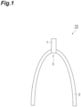
- FIG. 1 is a plan view schematically illustrating an electron source according to the present embodiment.
- An electron source 10 illustrated in FIG. 1 is provided with a LaB 6 tip 1, a tungsten filament 2, and a welding portion 3 in which a tip 1 and the tungsten filament 2 are directly bonded.
- the tip 1 is fixed by welding to an apex portion of the tungsten filament 2 bent in a loop shape.
- Devices provided with the electron source 10 include electron microscopes, semiconductor manufacturing devices, inspection devices, and machining devices.
- the tip 1 emits electrons through heating by means of electrification of the tungsten filament 2. It is preferable that the tip 1 be made of a LaB 6 single crystal substance and be a single crystal substance that is machined such that a ⁇ 100> orientation in which electrons are likely to be emitted coincides with an electron emission direction. It is preferable that a side surface of the tip 1 be a crystal plane which is a (100) plane since it is considered that this slows down an evaporation rate.
- the tip 1 has substantially a rectangular parallelepiped shape. A distal end portion of the tip 1 may be machined into a conical shape or a pyramid shape. In addition, the shape of the tip 1 is not particularly limited and can be formed into a desired shape by electric discharge machining or the like.
- the tungsten filament 2 is used for heating the tip 1 by means of electrification.
- the tungsten filament 2 may include elements other than tungsten (for example, rhenium, aluminum, silicon, and potassium) in accordance with the required performance.
- the tungsten filament 2 may be doped with an alkali metal (for example, potassium) for structure stabilization.
- the rhenium content of the tungsten filament 2 is 2 to 30 mass%, and for example, it may be 2 to 10 mass% or 2 to 5 mass%. Rhenium exhibits an effect of increasing the electrical resistivity of the tungsten filament 2.
- the welding portion 3 is a part in which the tip 1 and the tungsten filament 2 are bonded by welding.
- the welding portion 3 is formed when at least one of the tip 1 and the tungsten filament 2 is temporarily melted through heating and then solidified.
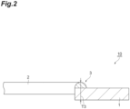
- a thickness of the welding portion 3 (a thickness T3 in FIG. 2 ) is 50 to 500 ⁇ m, and for example, it may be 50 to 400 ⁇ m or 110 to 250 ⁇ m.
- a melting point of the tip 1 is approximately 2,210°C, for example.
- a melting point of the tungsten filament 2 is approximately 3,422°C, for example.
- the electron source 10 is manufactured through the following steps.
- a thickness of the welding object 5 (the total thickness of the tip 1 and the tungsten filament 2, a thickness T5 in (a) in FIG. 3 ) is within a range of 50 to 500 ⁇ m, is preferably 170 to 400 ⁇ m, and may be 180 to 350 ⁇ m or 180 to 280 ⁇ m.
- the thickness of the welding object 5 is the same, in the step (A), as a separation distance between the pair of welding electrodes 6a and 6b sandwiching the welding object 5.
- the welding object 5 When the thickness of the welding object 5 (the separation distance of the pair of welding electrodes 6a and 6b) is within the foregoing range, the welding object 5 can be locally heated to a high temperature by means of electrification using the pair of welding electrodes 6a and 6b, and thus the tip 1 and the tungsten filament 2 can be firmly bonded by welding.
- a cross-sectional shape of a part in the tip 1 welded to the tungsten filament 2 is a square shape or a rectangular shape of which a length of one side is 10 to 300 ⁇ m, for example.
- the length of one side is preferably 60 to 250 ⁇ m and may be 60 to 200 ⁇ m or 70 to 150 ⁇ m.
- a cross-sectional shape of a part in the tip 1 welded to the tungsten filament 2 may be a circular shape or an oval shape, for example.
- a thickness of the tip 1 in a welding direction (a thickness T1 in (a) in FIG. 3 ) is preferably 60 to 250 ⁇ m and may be 60 to 200 ⁇ m or 70 to 150 ⁇ m.
- the arrow A in (a) in FIG. 3 indicates "the welding direction".
- a cross-sectional shape of a part in the tungsten filament 2 welded to the tip 1 is a circular shape or an oval shape, for example.
- a thickness of the tungsten filament 2 in the welding direction (a thickness T2 in (a) in FIG. 3 ) is preferably 60 to 250 ⁇ m and may be 60 to 200 ⁇ m or 70 to 150 ⁇ m.
- a cross-sectional shape of a part in the tungsten filament 2 welded to the tip 1 may be a square shape or a rectangular shape, for example. In this case, the thickness of the tungsten filament 2 in the welding direction is preferably 60 to 250 ⁇ m and may be 60 to 200 ⁇ m or 70 to 150 ⁇ m.
- a ratio T1/T2 of the thickness T1 of the tip 1 to the thickness T2 of the tungsten filament 2 is preferably 0.6 to 1.4 and is more preferably 0.8 to 1.3.
- the ratio T1/T2 is within the foregoing range, a region including an interface between the tip 1 and the tungsten filament 2 in the welding object 5 can be efficiently heated to a high temperature.
- the heating temperature can be adjusted by adjusting currents flowing from the pair of welding electrodes 6a and 6b to the welding object 5.
- the tip 1 and the tungsten filament 2 need only be locally melted, and it is preferable that both the tip 1 and the tungsten filament 2 be locally melted.
- Pressing forces applied from the pair of welding electrodes 6a and 6b to the welding object 5 need only be set to a strength and a time sufficient for the tip 1 and the tungsten filament 2 to be firmly bonded.
- the arrow E in (b) in FIG. 3 indicates a direction in which a current flows, and the arrow F indicates a direction of a pressing force.
- a form in which the tip 1 is embedded into the tungsten filament 2 may be adopted as illustrated in FIG. 2 , or a form in which the tip 1 is bonded to a surface of a tungsten filament 2A may be adopted as illustrated in FIG. 4 .
- the tungsten filament 2A illustrated in FIG. 4 has a quadrangular cross section.
- the tip 1 is constituted using a LaB 6 single crystal substance
- the tip 1 may be constituted using a HfC single crystal (melting point: 3,890°C) or may be constituted using an IrCe compound (for example, Ir 2 Ce, Ir 3 Ce, Ir 7 Ce 2 , or Ir 5 Ce). Even when these electron emission materials are used as the tip 1, a tip and a tungsten filament can be firmly bonded by welding.
- a LaB 6 tip and a tungsten filament having the following size were prepared.
- the tip and the tungsten filament were directly welded as follows. First, in a state where the tip and the tungsten filament overlapped in direct contact, these were sandwiched between a pair of welding electrodes (refer to (a) in FIG. 3 ). The tip and the tungsten filament were welded by causing a current to flow while pressing forces are applied to both of them by the pair of welding electrodes (refer to (b) in FIG. 3 ). The welding current was set such that the temperature at the interface between the tip and the tungsten filament exceeded 3,422°C (the melting point of tungsten). As a result, as shown in the SEM photograph of FIG. 5 , an electron source having both of them firmly bonded in a state where the tip was embedded into the tungsten filament was obtained.
- a LaB 6 tip and a tungsten filament having the following size were prepared.
- a HfC tip and a tungsten filament having the following size were prepared.
- Example 2 Similar to Example 1, welding of the tip and the tungsten filament was attempted.
- the welding current was set such that the temperature at the interface between the tip and the tungsten filament exceeded 3,422°C (the melting point of tungsten).
- 3,422°C the melting point of tungsten
- IrCe compound (Ir 7 Ce 2 ) tip and a tungsten filament having the following size were prepared.
- Example 2 Similar to Example 1, welding of the tip and the tungsten filament was attempted.
- the welding current was set such that the temperature at the interface between the tip and the tungsten filament exceeded 3,422°C (the melting point of tungsten).
- 3,422°C the melting point of tungsten
Landscapes
- Chemical & Material Sciences (AREA)
- Analytical Chemistry (AREA)
- Solid Thermionic Cathode (AREA)
- Electron Sources, Ion Sources (AREA)
- Cold Cathode And The Manufacture (AREA)
Abstract
Description
- The present disclosure relates to an electron source, a method for manufacturing the same, and a device provided with the electron source.
- Electron sources are used in electron microscopes and semiconductor inspection devices, for example. An electron source is provided with a tip constituted using an electron emission material. Specific examples of an electron emission material include a LaB6 (lanthanum hexaboride) single crystal, a HfC single crystal, and an IrCe compound.
- For example, an electron source using a LaB6 single crystal is constituted of a LaB6 single crystal tip, a tungsten filament for heating this tip by means of electrification, and a bonding material for fixing the tip to the tungsten filament. Manufacturing Example 1 of
Patent Literature 1 discloses that an intermediate layer is provided using a paste including TaC powder on a side surface of a lower portion of a LaB6 single crystal tip and a support metal layer is provided using a Ta foil. In this Manufacturing Example 1, a thermo-electronic emission cathode is assembled by spot-welding a W wire having a diameter of 150 µm to the support metal layer.Patent Literature 2 discloses a sintering material for an electron beam generation cathode member including 90 mass% or more of a compound consisting of iridium and cerium. -
- [Patent Literature 1]
Japanese Unexamined Patent Publication No. H1-7450 - [Patent Literature 2]
Japanese Patent No. 6805306 - As in Manufacturing Example 1 of
Patent Literature 1, when a layer including tantalum (Ta) is interposed between a LaB6 tip and a tungsten filament (W wire), the degree of vacuum deteriorates due to a reaction of tantalum with LaB6 at the time of electrification and heating, and this may cause emission instability of a cathode. For this reason, it is desirable to have a structure in which a tip of an electron emission material is directly bonded to a tungsten filament. However, in the related art, a tip of an electron emission material and a tungsten filament cannot be firmly bonded by welding, and there is a risk that the tip may fall. For this reason, an electron source having such a structure has not been put to practical use. - The present disclosure provides a method for manufacturing an electron source having a structure in which a tip of an electron emission material is directly bonded to a tungsten filament. In addition, the present disclosure provides an electron source, in which deterioration in degree of vacuum can be curbed compared to electron sources in the related art using tantalum for fixing a tip and a stable emission current can be obtained, and a device provided with the same.
- A method for manufacturing an electron source according to an aspect of the present disclosure includes steps of: sandwiching a welding object in which a tip of an electron emission material and a tungsten filament overlap in direct contact between a pair of welding electrodes; and welding the tip and the tungsten filament by causing a current to flow while pressing forces are applied to the welding object by the pair of welding electrodes. A thickness of the welding object is within a range of 50 to 500 µm. Examples of the electron emission material include a LaB6 single crystal, a HfC single crystal, and an IrCe compound. An IrCe compound is Ir2Ce, Ir3Ce, Ir7Ce2, or Ir5Ce, for example.
- The inventors attempted to directly weld a tip of an electron emission material (LaB6 single crystal) and a tungsten filament using a resistance welding machine having the constitution illustrated in (a) and (b) in
FIGS. 3 . As a result, if a thickness of a welding object (the total thickness of the tip and the tungsten filament) was within a range of 50 to 500 µm, the welding object could be locally heated to a high temperature by means of electrification using a pair of welding electrodes, and thus the tip and the tungsten filament could be firmly bonded by welding. - A cross-sectional shape of a part in the tip welded to the tungsten filament is a square shape or a rectangular shape of which a length of one side is 10 to 300 µm, for example.
- An electron source according to another aspect of the present disclosure includes a tip of an electron emission material, a tungsten filament, and a welding portion in which the tip and the tungsten filament are directly bonded. The thickness of the welding portion is 50 to 500 µm. Since the tip and the tungsten filament are directly bonded, deterioration in degree of vacuum can be curbed compared to electron sources in the related art having a layer including tantalum interposed between both of them, and a stable emission current can be obtained.
- The tungsten filament according to the present disclosure may include elements other than tungsten (for example, rhenium, aluminum, silicon, and potassium) in accordance with the required performance.
- A device according to another aspect of the present disclosure includes the foregoing electron source. Examples of a device provided with an electron source include electron microscopes, semiconductor manufacturing devices, and inspection devices.
- According to the present disclosure, a method for manufacturing an electron source having a structure in which a tip of an electron emission material is directly bonded to a tungsten filament is provided. In addition, according to the present disclosure, an electron source, in which deterioration in degree of vacuum can be curbed compared to electron sources in the related art using tantalum for fixing a tip and a stable emission current can be obtained, and a device provided with the same are provided.
-
-
FIG. 1 is a plan view schematically illustrating an embodiment of an electron source according to the present disclosure. -
FIG. 2 is a cross-sectional view schematically illustrating a welding portion in the electron source illustrated inFIG. 1 . - (a) in
FIG. 3 is a cross-sectional view schematically illustrating a state where a welding object in which a tip and a tungsten filament overlap in direct contact is sandwiched between a pair of welding electrodes, and (b) inFIG. 3 is a cross-sectional view schematically illustrating a condition in which the tip and the tungsten filament are welded by causing a current to flow while pressing forces are applied to the welding object by the pair of welding electrodes. -
FIG. 4 is a cross-sectional view schematically illustrating another form of a welding portion in the electron source. -
FIG. 5 is an SEM photograph showing the electron source according to Example 1. -
FIG. 6 is an SEM photograph showing the electron source according to Example 2. -
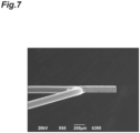
FIG. 7 is an SEM photograph showing the electron source according to Example 3. - Hereinafter, with reference to the drawings, an embodiment of the present disclosure will be described. In the following description, the same reference signs are used for the same elements or elements having the same function, and duplicate description thereof will be omitted. The present invention is not limited to the following embodiment.
-
FIG. 1 is a plan view schematically illustrating an electron source according to the present embodiment. Anelectron source 10 illustrated inFIG. 1 is provided with a LaB6 tip 1, atungsten filament 2, and awelding portion 3 in which atip 1 and thetungsten filament 2 are directly bonded. Thetip 1 is fixed by welding to an apex portion of thetungsten filament 2 bent in a loop shape. Devices provided with theelectron source 10 include electron microscopes, semiconductor manufacturing devices, inspection devices, and machining devices. - The
tip 1 emits electrons through heating by means of electrification of thetungsten filament 2. It is preferable that thetip 1 be made of a LaB6 single crystal substance and be a single crystal substance that is machined such that a <100> orientation in which electrons are likely to be emitted coincides with an electron emission direction. It is preferable that a side surface of thetip 1 be a crystal plane which is a (100) plane since it is considered that this slows down an evaporation rate. Thetip 1 has substantially a rectangular parallelepiped shape. A distal end portion of thetip 1 may be machined into a conical shape or a pyramid shape. In addition, the shape of thetip 1 is not particularly limited and can be formed into a desired shape by electric discharge machining or the like. - The
tungsten filament 2 is used for heating thetip 1 by means of electrification. Thetungsten filament 2 may include elements other than tungsten (for example, rhenium, aluminum, silicon, and potassium) in accordance with the required performance. Thetungsten filament 2 may be doped with an alkali metal (for example, potassium) for structure stabilization. When thetungsten filament 2 includes rhenium, the rhenium content of thetungsten filament 2 is 2 to 30 mass%, and for example, it may be 2 to 10 mass% or 2 to 5 mass%. Rhenium exhibits an effect of increasing the electrical resistivity of thetungsten filament 2. - The
welding portion 3 is a part in which thetip 1 and thetungsten filament 2 are bonded by welding. Thewelding portion 3 is formed when at least one of thetip 1 and thetungsten filament 2 is temporarily melted through heating and then solidified. A thickness of the welding portion 3 (a thickness T3 inFIG. 2 ) is 50 to 500 µm, and for example, it may be 50 to 400 µm or 110 to 250 µm. A melting point of thetip 1 is approximately 2,210°C, for example. A melting point of thetungsten filament 2 is approximately 3,422°C, for example. - Next, a method for manufacturing the
electron source 10 will be described. Theelectron source 10 is manufactured through the following steps. - (A) A step of sandwiching a
welding object 5 in which thetip 1 and thetungsten filament 2 overlap in direct contact between a pair ofwelding electrodes FIG. 3 ) - (B) A step of welding the
tip 1 and thetungsten filament 2 by causing a current to flow while pressing forces are applied to thewelding object 5 by the pair ofwelding electrodes FIG. 3 ) - In the step (A), a thickness of the welding object 5 (the total thickness of the
tip 1 and thetungsten filament 2, a thickness T5 in (a) inFIG. 3 ) is within a range of 50 to 500 µm, is preferably 170 to 400 µm, and may be 180 to 350 µm or 180 to 280 µm. The thickness of thewelding object 5 is the same, in the step (A), as a separation distance between the pair ofwelding electrodes welding object 5. When the thickness of the welding object 5 (the separation distance of the pair ofwelding electrodes welding object 5 can be locally heated to a high temperature by means of electrification using the pair ofwelding electrodes tip 1 and thetungsten filament 2 can be firmly bonded by welding. - A cross-sectional shape of a part in the
tip 1 welded to thetungsten filament 2 is a square shape or a rectangular shape of which a length of one side is 10 to 300 µm, for example. The length of one side is preferably 60 to 250 µm and may be 60 to 200 µm or 70 to 150 µm. A cross-sectional shape of a part in thetip 1 welded to thetungsten filament 2 may be a circular shape or an oval shape, for example. In this case, a thickness of thetip 1 in a welding direction (a thickness T1 in (a) inFIG. 3 ) is preferably 60 to 250 µm and may be 60 to 200 µm or 70 to 150 µm. The arrow A in (a) inFIG. 3 indicates "the welding direction". - A cross-sectional shape of a part in the
tungsten filament 2 welded to thetip 1 is a circular shape or an oval shape, for example. A thickness of thetungsten filament 2 in the welding direction (a thickness T2 in (a) inFIG. 3 ) is preferably 60 to 250 µm and may be 60 to 200 µm or 70 to 150 µm. A cross-sectional shape of a part in thetungsten filament 2 welded to thetip 1 may be a square shape or a rectangular shape, for example. In this case, the thickness of thetungsten filament 2 in the welding direction is preferably 60 to 250 µm and may be 60 to 200 µm or 70 to 150 µm. - A ratio T1/T2 of the thickness T1 of the
tip 1 to the thickness T2 of thetungsten filament 2 is preferably 0.6 to 1.4 and is more preferably 0.8 to 1.3. When the ratio T1/T2 is within the foregoing range, a region including an interface between thetip 1 and thetungsten filament 2 in thewelding object 5 can be efficiently heated to a high temperature. - In the step (B), the heating temperature can be adjusted by adjusting currents flowing from the pair of
welding electrodes welding object 5. Through heating by means of electrification, at least one of thetip 1 and thetungsten filament 2 need only be locally melted, and it is preferable that both thetip 1 and thetungsten filament 2 be locally melted. Pressing forces applied from the pair ofwelding electrodes welding object 5 need only be set to a strength and a time sufficient for thetip 1 and thetungsten filament 2 to be firmly bonded. The arrow E in (b) inFIG. 3 indicates a direction in which a current flows, and the arrow F indicates a direction of a pressing force. - Regarding the electron source manufactured through the step (B), a form in which the
tip 1 is embedded into thetungsten filament 2 may be adopted as illustrated inFIG. 2 , or a form in which thetip 1 is bonded to a surface of atungsten filament 2A may be adopted as illustrated inFIG. 4 . Thetungsten filament 2A illustrated inFIG. 4 has a quadrangular cross section. - In the foregoing embodiment, a form in which the
tip 1 is constituted using a LaB6 single crystal substance has been described as an example. However, thetip 1 may be constituted using a HfC single crystal (melting point: 3,890°C) or may be constituted using an IrCe compound (for example, Ir2Ce, Ir3Ce, Ir7Ce2, or Ir5Ce). Even when these electron emission materials are used as thetip 1, a tip and a tungsten filament can be firmly bonded by welding. - Hereinafter, the present disclosure will be described on the basis of examples and a comparative example. The present invention is not limited to the following examples.
- A LaB6 tip and a tungsten filament having the following size were prepared.
-
- Thickness T1: 90 µm
- Width: 90 µm
- Length: 1,000 µm
-
- Diameter (thickness T2): 127 µm
- Purity of tungsten: 99.999 mass% or more
- The tip and the tungsten filament were directly welded as follows. First, in a state where the tip and the tungsten filament overlapped in direct contact, these were sandwiched between a pair of welding electrodes (refer to (a) in
FIG. 3 ). The tip and the tungsten filament were welded by causing a current to flow while pressing forces are applied to both of them by the pair of welding electrodes (refer to (b) inFIG. 3 ). The welding current was set such that the temperature at the interface between the tip and the tungsten filament exceeded 3,422°C (the melting point of tungsten). As a result, as shown in the SEM photograph ofFIG. 5 , an electron source having both of them firmly bonded in a state where the tip was embedded into the tungsten filament was obtained. - A LaB6 tip and a tungsten filament having the following size were prepared.
-
- Thickness T1: 500 µm
- Width: 750 µm
- Length: 1,500 µm
-
- Diameter (thickness T2): 127 µm
- Purity of tungsten: 99.999 mass% or more
- Similar to Example 1, welding of the tip and the tungsten filament was attempted. Although the tip and the tungsten filament were heated while variously changing the setting of the welding current, both of them could not be welded.
- A HfC tip and a tungsten filament having the following size were prepared.
-
- Thickness T1: 90 µm
- Width: 90 µm
- Length: 1,000 µm
-
- Diameter (thickness T2): 127 µm
- Purity of tungsten: 99.999 mass% or more
- Similar to Example 1, welding of the tip and the tungsten filament was attempted. The welding current was set such that the temperature at the interface between the tip and the tungsten filament exceeded 3,422°C (the melting point of tungsten). As a result, as shown in the SEM photograph of
FIG. 6 , an electron source having both of them firmly bonded in a state where a part of the tip was embedded into the tungsten filament was obtained. - An IrCe compound (Ir7Ce2) tip and a tungsten filament having the following size were prepared.
-
- Thickness T1: 90 µm
- Width: 90 µm
- Length: 1,000 µm
-
- Diameter (thickness T2): 127 µm
- Purity of tungsten: 99.999 mass% or more
- Similar to Example 1, welding of the tip and the tungsten filament was attempted. The welding current was set such that the temperature at the interface between the tip and the tungsten filament exceeded 3,422°C (the melting point of tungsten). As a result, as shown in the SEM photograph of
FIG. 7 , an electron source having both of them firmly bonded in a state where the tip was embedded into the tungsten filament was obtained. -
- 1 Tip
- 2, 2A Tungsten filament
- 3 Welding portion
- 5 Welding object
- 6a, 6b Pair of welding electrodes
- 10 Electron source
Claims (8)
- A method for manufacturing an electron source, the method comprising steps of:sandwiching a welding object in which a tip of an electron emission material and a tungsten filament overlap in direct contact between a pair of welding electrodes; andwelding the tip and the tungsten filament by causing a current to flow while pressing forces are applied to the welding object by the pair of welding electrodes,wherein a thickness of the welding object is within a range of 50 to 500 µm.
- The method for manufacturing an electron source according to claim 1, wherein a cross-sectional shape of a part welded to the tungsten filament in the tip is a square shape or a rectangular shape in which a length of one side is 10 to 300 µm.
- The method for manufacturing an electron source according to claim 1 or 2, wherein the electron emission material is one kind selected from the group consisting of LaB6, HfC, and an IrCe compound.
- The method for manufacturing an electron source according to any one of claims 1 to 3, wherein the tungsten filament contains rhenium.
- An electron source comprising:a tip of an electron emission material;a tungsten filament; anda welding portion in which the tip and the tungsten filament are directly bonded,wherein a thickness of the welding portion is 50 to 500 µm.
- The electron source according to claim 5, wherein the electron emission material is one kind selected from the group consisting of LaB6, HfC, and an IrCe compound.
- The electron source according to claim 5 or 6, wherein the tungsten filament contains rhenium.
- A device comprising the electron source according to any one of claims 5 to 7.
Applications Claiming Priority (2)
| Application Number | Priority Date | Filing Date | Title |
|---|---|---|---|
| JP2020217530 | 2020-12-25 | ||
| PCT/JP2021/047021 WO2022138558A1 (en) | 2020-12-25 | 2021-12-20 | Electron source, method for manufacturing same, and device provided with electron source |
Publications (2)
| Publication Number | Publication Date |
|---|---|
| EP4270441A1 true EP4270441A1 (en) | 2023-11-01 |
| EP4270441A4 EP4270441A4 (en) | 2024-05-22 |
Family
ID=82157950
Family Applications (1)
| Application Number | Title | Priority Date | Filing Date |
|---|---|---|---|
| EP21910702.6A Withdrawn EP4270441A4 (en) | 2020-12-25 | 2021-12-20 | Electron source, method for manufacturing same, and device provided with electron source |
Country Status (6)
| Country | Link |
|---|---|
| US (1) | US12014894B2 (en) |
| EP (1) | EP4270441A4 (en) |
| JP (2) | JPWO2022138558A1 (en) |
| CN (1) | CN116325060A (en) |
| TW (1) | TW202230422A (en) |
| WO (1) | WO2022138558A1 (en) |
Families Citing this family (3)
| Publication number | Priority date | Publication date | Assignee | Title |
|---|---|---|---|---|
| JPWO2022138558A1 (en) | 2020-12-25 | 2022-06-30 | ||
| JP7783574B2 (en) * | 2022-03-10 | 2025-12-10 | 三菱自動車工業株式会社 | battery pack |
| JP2025054954A (en) * | 2023-09-27 | 2025-04-08 | 浜松ホトニクス株式会社 | Electron source, electron gun and device using same |
Family Cites Families (19)
| Publication number | Priority date | Publication date | Assignee | Title |
|---|---|---|---|---|
| JPS5046477A (en) * | 1973-08-31 | 1975-04-25 | ||
| JPS51105760A (en) * | 1975-03-14 | 1976-09-18 | Hitachi Ltd | CHOKUNETSUGATAHOKABUTSUINKYOKU NO SEIZOHOHO |
| US4055780A (en) * | 1975-04-10 | 1977-10-25 | National Institute For Researches In Inorganic Materials | Thermionic emission cathode having a tip of a single crystal of lanthanum hexaboride |
| US4258283A (en) * | 1978-08-31 | 1981-03-24 | Balzers Aktiengesellschaft Fur Hochvakuumtechnik Und Dunne Schichten | Cathode for electron emission |
| JPS61155851A (en) | 1984-12-28 | 1986-07-15 | Kuraray Co Ltd | Semiconductor ion sensor |
| JPS647450A (en) | 1987-06-30 | 1989-01-11 | Ube Industries | Pointed thermionic emission cathode |
| JP2000246451A (en) * | 1999-03-04 | 2000-09-12 | Noritake Co Ltd | Welding machine for oxide-covered filament |
| US6771013B2 (en) | 2000-10-17 | 2004-08-03 | Fei Company | Low power schottky emitter |
| JP2002358922A (en) * | 2001-05-31 | 2002-12-13 | Sanken Electric Co Ltd | Cold cathode discharge tube and manufacturing method of same |
| JP5131735B2 (en) * | 2007-04-12 | 2013-01-30 | 独立行政法人物質・材料研究機構 | Manufacturing method of surface emitter, manufacturing method of point emitter, and structure |
| WO2009044564A1 (en) | 2007-10-05 | 2009-04-09 | Denki Kagaku Kogyo Kabushiki Kaisha | Electron source and electron beam device |
| JP2010015966A (en) * | 2008-06-06 | 2010-01-21 | Hitachi High-Technologies Corp | Electron-emitting element, electron gun, electron microscope device using it, and electron beam lithogrphy device |
| JP2010238384A (en) * | 2009-03-30 | 2010-10-21 | Denki Kagaku Kogyo Kk | Electron source and its use |
| US8896195B2 (en) * | 2010-10-21 | 2014-11-25 | Hermes Microvision, Inc. | Filament for electron source |
| US9165737B2 (en) * | 2012-10-04 | 2015-10-20 | Nuflare Technology, Inc. | High-brightness, long life thermionic cathode and methods of its fabrication |
| JP2015043394A (en) * | 2013-08-26 | 2015-03-05 | 株式会社ニューフレアテクノロジー | Method for manufacturing thermionic emission source and method for manufacturing cathode |
| JP6636472B2 (en) * | 2017-02-28 | 2020-01-29 | 株式会社日立ハイテクノロジーズ | Electron source and electron beam device using the same |
| JP6805306B1 (en) * | 2019-09-02 | 2020-12-23 | 株式会社コベルコ科研 | A sintered material for a cathode member for generating an electron beam, a method for producing a molten material used for producing the sintered material, and a method for producing the sintered material. |
| JPWO2022138558A1 (en) | 2020-12-25 | 2022-06-30 |
-
2021
- 2021-12-20 JP JP2022522320A patent/JPWO2022138558A1/ja active Pending
- 2021-12-20 WO PCT/JP2021/047021 patent/WO2022138558A1/en not_active Ceased
- 2021-12-20 EP EP21910702.6A patent/EP4270441A4/en not_active Withdrawn
- 2021-12-20 US US18/258,461 patent/US12014894B2/en active Active
- 2021-12-20 CN CN202180068505.XA patent/CN116325060A/en active Pending
- 2021-12-21 TW TW110147833A patent/TW202230422A/en unknown
-
2022
- 2022-12-23 JP JP2022207163A patent/JP7781050B2/en active Active
Also Published As
| Publication number | Publication date |
|---|---|
| JP7781050B2 (en) | 2025-12-05 |
| JPWO2022138558A1 (en) | 2022-06-30 |
| TW202230422A (en) | 2022-08-01 |
| EP4270441A4 (en) | 2024-05-22 |
| JP2023036830A (en) | 2023-03-14 |
| WO2022138558A1 (en) | 2022-06-30 |
| US12014894B2 (en) | 2024-06-18 |
| US20240029989A1 (en) | 2024-01-25 |
| CN116325060A (en) | 2023-06-23 |
Similar Documents
| Publication | Publication Date | Title |
|---|---|---|
| US12014894B2 (en) | Electron source, method for manufacturing same, and device provided with electron source | |
| US8016633B2 (en) | Method for making field emission device incorporating a carbon nanotube yarn | |
| US9029795B2 (en) | Radiation generating tube, and radiation generating device and apparatus including the tube | |
| US8896195B2 (en) | Filament for electron source | |
| US10763069B2 (en) | X-ray tube and method of manufacturing the same | |
| EP2377141B1 (en) | Electron source and cathode cup thereof | |
| EP1892741B1 (en) | Diamond electron emission cathode, electron emission source, electron microscope, and electron beam exposure device | |
| US11915921B2 (en) | Electron source, method for manufacturing same, emitter, and device including same | |
| US12293893B2 (en) | Electron source, manufacturing method therefor, and device comprising electron source | |
| TW202546878A (en) | Cold field emitter assembly | |
| EP4303906B1 (en) | Emitter and device provided with same | |
| JP7640787B2 (en) | Electron source and manufacturing method thereof, emitter and device including same | |
| KR102832184B1 (en) | Liquid metal ion source device for using bismuth and its alloy | |
| US8072146B2 (en) | Fluorescent lamp | |
| JP2024121498A (en) | Emitter | |
| JP2003036795A (en) | Vacuum micro device, circuit and device provided with the device | |
| JP2009117204A (en) | Electron source and manufacturing method thereof |
Legal Events
| Date | Code | Title | Description |
|---|---|---|---|
| STAA | Information on the status of an ep patent application or granted ep patent |
Free format text: STATUS: THE INTERNATIONAL PUBLICATION HAS BEEN MADE |
|
| PUAI | Public reference made under article 153(3) epc to a published international application that has entered the european phase |
Free format text: ORIGINAL CODE: 0009012 |
|
| STAA | Information on the status of an ep patent application or granted ep patent |
Free format text: STATUS: REQUEST FOR EXAMINATION WAS MADE |
|
| 17P | Request for examination filed |
Effective date: 20230713 |
|
| AK | Designated contracting states |
Kind code of ref document: A1 Designated state(s): AL AT BE BG CH CY CZ DE DK EE ES FI FR GB GR HR HU IE IS IT LI LT LU LV MC MK MT NL NO PL PT RO RS SE SI SK SM TR |
|
| DAV | Request for validation of the european patent (deleted) | ||
| DAX | Request for extension of the european patent (deleted) | ||
| REG | Reference to a national code |
Ref country code: DE Ref legal event code: R079 Free format text: PREVIOUS MAIN CLASS: H01J0037060000 Ipc: H01J0001148000 |
|
| A4 | Supplementary search report drawn up and despatched |
Effective date: 20240424 |
|
| RIC1 | Information provided on ipc code assigned before grant |
Ipc: H01J 37/065 20060101ALI20240418BHEP Ipc: H01J 9/04 20060101ALI20240418BHEP Ipc: H01J 1/18 20060101ALI20240418BHEP Ipc: H01J 1/148 20060101AFI20240418BHEP |
|
| STAA | Information on the status of an ep patent application or granted ep patent |
Free format text: STATUS: EXAMINATION IS IN PROGRESS |
|
| 17Q | First examination report despatched |
Effective date: 20241029 |
|
| GRAP | Despatch of communication of intention to grant a patent |
Free format text: ORIGINAL CODE: EPIDOSNIGR1 |
|
| STAA | Information on the status of an ep patent application or granted ep patent |
Free format text: STATUS: GRANT OF PATENT IS INTENDED |
|
| INTG | Intention to grant announced |
Effective date: 20250723 |
|
| STAA | Information on the status of an ep patent application or granted ep patent |
Free format text: STATUS: THE APPLICATION IS DEEMED TO BE WITHDRAWN |
|
| 18D | Application deemed to be withdrawn |
Effective date: 20251125 |