EP4269331B1 - Verfahren zur herstellung einer mems-vorrichtung - Google Patents
Verfahren zur herstellung einer mems-vorrichtung Download PDFInfo
- Publication number
- EP4269331B1 EP4269331B1 EP23170086.5A EP23170086A EP4269331B1 EP 4269331 B1 EP4269331 B1 EP 4269331B1 EP 23170086 A EP23170086 A EP 23170086A EP 4269331 B1 EP4269331 B1 EP 4269331B1
- Authority
- EP
- European Patent Office
- Prior art keywords
- semiconductor layer
- layer
- elements
- contact
- upper face
- Prior art date
- Legal status (The legal status is an assumption and is not a legal conclusion. Google has not performed a legal analysis and makes no representation as to the accuracy of the status listed.)
- Active
Links
Images


Classifications
-
- B—PERFORMING OPERATIONS; TRANSPORTING
- B81—MICROSTRUCTURAL TECHNOLOGY
- B81C—PROCESSES OR APPARATUS SPECIALLY ADAPTED FOR THE MANUFACTURE OR TREATMENT OF MICROSTRUCTURAL DEVICES OR SYSTEMS
- B81C1/00—Manufacture or treatment of devices or systems in or on a substrate
- B81C1/00015—Manufacture or treatment of devices or systems in or on a substrate for manufacturing microsystems
- B81C1/00134—Manufacture or treatment of devices or systems in or on a substrate for manufacturing microsystems comprising flexible or deformable structures
- B81C1/00182—Arrangements of deformable or non-deformable structures, e.g. membrane and cavity for use in a transducer
-
- B—PERFORMING OPERATIONS; TRANSPORTING
- B81—MICROSTRUCTURAL TECHNOLOGY
- B81C—PROCESSES OR APPARATUS SPECIALLY ADAPTED FOR THE MANUFACTURE OR TREATMENT OF MICROSTRUCTURAL DEVICES OR SYSTEMS
- B81C1/00—Manufacture or treatment of devices or systems in or on a substrate
- B81C1/00777—Preserve existing structures from alteration, e.g. temporary protection during manufacturing
- B81C1/00785—Avoid chemical alteration, e.g. contamination, oxidation or unwanted etching
- B81C1/00801—Avoid alteration of functional structures by etching, e.g. using a passivation layer or an etch stop layer
-
- B—PERFORMING OPERATIONS; TRANSPORTING
- B81—MICROSTRUCTURAL TECHNOLOGY
- B81C—PROCESSES OR APPARATUS SPECIALLY ADAPTED FOR THE MANUFACTURE OR TREATMENT OF MICROSTRUCTURAL DEVICES OR SYSTEMS
- B81C1/00—Manufacture or treatment of devices or systems in or on a substrate
- B81C1/00349—Creating layers of material on a substrate
- B81C1/00357—Creating layers of material on a substrate involving bonding one or several substrates on a non-temporary support, e.g. another substrate
-
- B—PERFORMING OPERATIONS; TRANSPORTING
- B81—MICROSTRUCTURAL TECHNOLOGY
- B81C—PROCESSES OR APPARATUS SPECIALLY ADAPTED FOR THE MANUFACTURE OR TREATMENT OF MICROSTRUCTURAL DEVICES OR SYSTEMS
- B81C2201/00—Manufacture or treatment of microstructural devices or systems
- B81C2201/01—Manufacture or treatment of microstructural devices or systems in or on a substrate
- B81C2201/0101—Shaping material; Structuring the bulk substrate or layers on the substrate; Film patterning
- B81C2201/0128—Processes for removing material
- B81C2201/013—Etching
- B81C2201/0132—Dry etching, i.e. plasma etching, barrel etching, reactive ion etching [RIE], sputter etching or ion milling
-
- B—PERFORMING OPERATIONS; TRANSPORTING
- B81—MICROSTRUCTURAL TECHNOLOGY
- B81C—PROCESSES OR APPARATUS SPECIALLY ADAPTED FOR THE MANUFACTURE OR TREATMENT OF MICROSTRUCTURAL DEVICES OR SYSTEMS
- B81C2201/00—Manufacture or treatment of microstructural devices or systems
- B81C2201/01—Manufacture or treatment of microstructural devices or systems in or on a substrate
- B81C2201/0174—Manufacture or treatment of microstructural devices or systems in or on a substrate for making multi-layered devices, film deposition or growing
- B81C2201/019—Bonding or gluing multiple substrate layers
-
- B—PERFORMING OPERATIONS; TRANSPORTING
- B81—MICROSTRUCTURAL TECHNOLOGY
- B81C—PROCESSES OR APPARATUS SPECIALLY ADAPTED FOR THE MANUFACTURE OR TREATMENT OF MICROSTRUCTURAL DEVICES OR SYSTEMS
- B81C2201/00—Manufacture or treatment of microstructural devices or systems
- B81C2201/05—Temporary protection of devices or parts of the devices during manufacturing
- B81C2201/056—Releasing structures at the end of the manufacturing process
Definitions
- This description relates generally to electromechanical devices and in particular to devices based on microelectromechanical systems or MEMS (from the English “Micro Electro Mechanical Systems”). It applies in particular to devices based on micro- and nano-electromechanical systems or M&NEMS (from the English “Micro and Nano-ElectroMechanical Systems”).
- a MEMS device typically comprises at least one mechanical element, for example a seismic mass, having micrometric dimensions. This element can take various forms depending on the desired function of the device. MEMS devices can for example be used to implement measurement functions of various types, for example displacement or pressure measurements. MEMS devices are for example used in accelerometer-type sensors, gyrometers, pressure sensors, etc.
- the first, second and third semiconductor layers are made of silicon.
- the trench formation step is followed by a release step, in which the insulating layer is removed from under the mechanical element.
- the step of transferring the third semiconductor layer onto the second semiconductor layer is preceded by a step of cleaning by plasma treatment of the lower face of the third semiconductor layer and/or the upper face of the second semiconductor layer.
- the mechanical element has a thickness of between 10 ⁇ m and 300 ⁇ m, for example between 20 ⁇ m and 100 ⁇ m, for example between 30 ⁇ m and 80 ⁇ m, for example between 40 ⁇ m and 60 ⁇ m.
- the method further comprises, before the step of forming the second semiconductor layer, a step of localized etching of the first semiconductor layer so as to define in said first semiconductor layer electromechanical transduction elements of micron or submicron dimensions.
- the method comprises, after said localized etching step and before the step of forming the second semiconductor layer, a step of forming protective elements made of an insulating material located opposite said electromechanical transduction elements of micron or submicron dimensions.
- the protective elements are removed with the insulating layer during the release step.
- micro-electromechanical device comprising a mechanical element comprising, in its thickness, a first semiconductor layer, a second semiconductor layer formed by epitaxy on and in contact with the upper face of the first semiconductor layer, and a third semiconductor layer fixed, by molecular bonding, on and in contact with the upper face of the second semiconductor layer.
- the mechanical element has a thickness of between 10 ⁇ m and 300 ⁇ m, for example between 20 ⁇ m and 100 ⁇ m, for example between 30 ⁇ m and 80 ⁇ m, for example between 40 ⁇ m and 60 ⁇ m.
- the device further comprises electromechanical transduction elements of micron or submicron dimensions formed in the first semiconductor layer.
- FIG 1 , there figure 2 , there figure 3 , there figure 4 , there figure 5 , there figure 6 , there figure 7 and the figure 8 are sectional views partially and schematically illustrating successive steps of an example of a method of manufacturing a MEMS device according to one embodiment.
- the expressions “approximately”, “approximately”, “substantially”, and “of the order of” mean to within 10%, preferably to within 5%.
- the device produced is an M&NEMS device, comprising electromechanical transduction elements of micron or submicron dimensions, for example of nanometric dimensions, or NEMS elements, for example strain gauges or actuators, coupled to mechanical elements of micrometric dimensions or MEMS elements, for example a seismic mass.
- M&NEMS devices comprising electromechanical transduction elements of micron or submicron dimensions, for example of nanometric dimensions, or NEMS elements, for example strain gauges or actuators, coupled to mechanical elements of micrometric dimensions or MEMS elements, for example a seismic mass.
- NEMS elements for example strain gauges or actuators
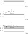
- FIG 1 represents a starting structure 11 of the SOI type (from the English “Semiconductor On Insulator”).
- the structure 11 comprises, for example, a support 13 made of a semiconductor material, topped with an electrically insulating layer 15, itself topped with a semiconductor layer 17.
- the support 13 is made of silicon.
- the support 13 has, for example, a thickness of between 200 ⁇ m and 800 ⁇ m, for example between 500 ⁇ m and 750 ⁇ m.
- the insulating layer 15 is made of an oxide, for example silicon oxide (SiO 2 ).
- the insulating layer 15 has for example a thickness of between 0.1 ⁇ m and 4 ⁇ m, for example between 0.3 ⁇ m and 3 ⁇ m, for example of the order of 2 ⁇ m.
- the semiconductor layer 17 is made of silicon, for example monocrystalline silicon.
- the semiconductor layer 17 has for example a thickness between 50 nm and 50 ⁇ m, for example between 200 nm and 2 ⁇ m, for example equal to approximately 250 nm or approximately 500 nm.
- the semiconductor layer 17 is doped.
- the insulating layer 15 is formed on and in contact with the support 13 such that the lower face of the insulating layer 15 is in contact with the upper face of the support 13.
- the semiconductor layer 17 is for example formed on and in contact with the insulating layer 15 such that the lower face of the semiconductor layer 17 is in contact with the upper face of the insulating layer 15.
- FIG 2 illustrates the structure obtained at the end of a localized etching step of the semiconductor layer 17 so as to form, in it, openings 19.
- the openings 19 pass, for example, right through the semiconductor layer 17, that is to say that they pass through the layer 17 over its entire thickness, so as to expose the upper face of the insulating layer 15.
- the openings 19 comprise in particular trenches 19a laterally delimiting one or more electromechanical transduction elements of micron or submicron dimensions (NEMS) 20 of the device.
- the elements 20 are for example strain gauges, for example resonant beams or piezoresistive gauges, each comprising one or more silicon bars of dimensions nanometric defined in the silicon layer 17 of the SOI structure.
- the openings 19 may further comprise at least one opening 19b intended to allow the subsequent resumption of an electrical contact on the underlying semiconductor support 13.
- the openings 19a and 19b are for example formed simultaneously during the same photolithography and etching step.
- FIG 3 illustrates the structure obtained at the end of a step of depositing an electrically insulating layer 21 on the upper face of the structure of the figure 2 .
- the insulating layer 21 extends for example continuously over the entire upper surface of the structure, that is to say, in this example, on the upper face of the semiconductor layer 17 and in the openings 19.
- the insulating layer 21 extends on and in contact with the upper face of the semiconductor layer 17 outside the openings 19, and on and in contact with the upper face of the insulating layer 15 and with the sides of the semiconductor layer 17 in the openings 19.
- the layer 21 is for example made of silicon oxide.
- the layer 21 has for example a thickness e1, measured above the surface of the conductive layer 17, between 50 nm and 2 ⁇ m, for example between 0.1 ⁇ m and 0.5 ⁇ m, for example of the order of 0.3 ⁇ m.
- the layer 21 completely fills the openings 19.
- the layer 21 has for example a substantially flat upper face extending continuously over the entire upper surface of the structure.
- FIG 4 illustrates the structure obtained at the end of a localized removal step of the insulating layer 21, by example by photolithography and etching.
- layer 21 is removed over substantially the entire upper face of the structure illustrated in figure 3 except opposite the NEMS elements 20 and the trenches 19a laterally delimiting these elements.
- the layer 21 is removed in the contact recovery opening(s) 19b.
- the etching continues through the insulating layer 15 of the SOI structure opposite the opening 19b, until the upper face of the substrate 13 is exposed and thus allows the recovery of an electrical contact called a ground contact on the substrate 13.
- FIG 5 illustrates the structure obtained at the end of an epitaxial deposition step of a semiconductor layer 17', for example in the same material as the layer 17, on the upper face of the structure of the figure 4 .
- the layer 17' extends continuously over the entire surface of the structure and in particular fills the openings 19b.
- the layer 17' comes into contact, by its lower face, with the upper face of the substrate 13.
- the layer 17' is formed by epitaxial growth from the upper face of the semiconductor layer 17.
- the layer 17' is for example monocrystalline over substantially the entire surface of the structure, except opposite the insulating protection regions 21p covering the NEMS elements 20 of the device, where the layer 17' may have a polycrystalline structure.
- the polycrystalline part of layer 17' located on and in contact with the 21p protective insulating regions of the NEMS elements is designated by the reference 23.
- layer 17' is doped in situ, for example, with boron, during its deposition.
- the upper face of the layer 17' may not be flat. Indeed, the growth does not necessarily have the same speed opposite the openings 19b, opposite the insulating protection regions 21p, and opposite the portions of the upper face of the layer 17 not coated by the insulating regions 21p.
- a step of planarization of the upper face of the layer 17' is implemented at the end of the deposition step.
- the layers 17 and 17' have, outside the openings 19b and the regions for forming the NEMS elements 20 of the device, a cumulative thickness e2, from the upper face of the buried insulating layer 15, of between 1 ⁇ m and 50 ⁇ m, for example of between 5 ⁇ m and 30 ⁇ m, for example of between 10 ⁇ m and 20 ⁇ m.
- the planarization step is performed by CMP (Chemical Mechanical Polishing).
- the planarization step is performed by mechanical polishing or grinding followed by dry polishing.
- the planarization step is performed by a combination of the techniques described above.
- FIG 6 illustrates the structure obtained at the end of a step of transferring a semiconductor layer 25 onto the upper face of the structure illustrated in figure 5 and more particularly, on the upper face of layer 17'.
- layer 25 is carried over and in contact with the upper face of the layer 17'.
- the semiconductor layer 25 is a semiconductor wafer or a part of a semiconductor wafer.
- the layer 25 is for example made of the same material as the layer 17', for example silicon.
- the layer 25 is preferably monocrystalline.
- the layer 25 is, for example doped.
- the layer 25 corresponds to the upper crystalline semiconductor layer of an SOI structure. In this case, the support substrate of the SOI structure can serve as a handle during the transfer.
- the support substrate and the buried insulating layer of the SOI structure can be removed so as to retain only the layer 25.
- the layer 25 corresponds to a part of the thickness of a solid semiconductor substrate.
- the substrate is first transferred and fixed on the upper face of layer 17', then thinned, for example by grinding and/or CMP, so as to retain only layer 25.
- the layer 25 is for example fixed by molecular bonding of its lower face with the upper face of the layer 17'.
- the bonding is for example a molecular bonding of the SAB type (from the English "Surface Activated Bonding"), that is to say that the transfer step is preceded by a step of preparation or cleaning of the bonding surface of the layer 25 and/or of the bonding surface of the layer 17', by plasma treatment.
- annealing may be provided, for example at a temperature of the order of 400°C.
- the layers 17, 17' and 25 have a cumulative thickness e3.
- the thickness e3 is, for example, determined according to the type of MEMS element that one seeks to produce.
- the thickness e3 corresponds, for example, to the final thickness of a mechanical element, for example a seismic mass, of a MEMS element of the device.
- the thickness e3 can be adjusted according to the type of application considered.
- the thickness e3 is, for example, between 10 ⁇ m and 300 ⁇ m, for example between 20 ⁇ m and 100 ⁇ m, for example between 30 ⁇ m and 80 ⁇ m, for example between 40 and 60 ⁇ m.
- FIG. 7 illustrates the structure obtained at the end of a localized etching step, from the upper face of layer 25, of the stack formed by layers 17, 17' and 25.
- the etching step is performed through a mask, for example a hard mask, made of an oxide, for example tetraethyl orthosilicate (TEOS).
- TEOS tetraethyl orthosilicate
- the etching of layers 25, 17' and 17 is, for example, a deep reactive ion etching (DRIE).
- DRIE deep reactive ion etching
- vertical openings and/or trenches 28 are formed in the stack of layers 25, 17' and 17.
- these trenches and/or openings open onto the upper face of layer 15 or onto the upper face of the protections 21p.
- the etching is for example a selective etching of the semiconductor material(s) of layers 17, 17' and 25 relative to the dielectric material of layer 15 and the protection elements 21.
- the trenches and openings 28 define and delimit laterally, in the stack of semiconductor layers 17, 17' and 25, MEMS elements comprising in particular a mechanical element 29, for example a seismic mass.
- the trenches and openings 28 further allow the upper face of the protection elements 21p to be exposed opposite the NEMS elements 20 of the device.
- the trenches and openings 28 further define, opposite the ground contact recovery opening 19b, a portion 30 of the stack of layers 17' and 17, also called the ground contact recovery region, in contact, by its lower face, with the substrate 13.
- the etching step described above is preceded by a step of forming pads 27, for example on and in contact with the upper face of the semiconductor layer 25, opposite portions of the layer 25 not removed during the subsequent etching step and outside the MEMS elements and in particular the mechanical element 29 of the device.
- the pads 27 are made of germanium and have, for example, a thickness of between 100 nm and 1 ⁇ m, for example of the order of 500 nm.
- the pads 27 allow, for example, the subsequent sealing of the structure obtained at the end of the method described in relation to the Figures 1 to 8 with a hood (not shown).
- FIG 8 illustrates the structure obtained at the end of a step of removing a portion of the layer 15 and the insulating protection regions 21p.
- the layer 15 and the protection elements 21p are selectively etched relative to the semiconductor layers 17, 17' and 25, so as to release the MEMS and NEMS elements of the device.
- the etching is a gaseous chemical etching.
- the etching is carried out under hydrogen fluoride (HF) vapor.
- the release has a speed of between 5 nm/min and 100 nm/min, for example of between 20 nm/min and 60 nm/min, for example of the order of 48 nm/min.
- the etching time can be controlled so as to retain portions of the dielectric layer 15 serving as anchoring or mechanical support for the MEMS and NEMS elements of the device.
- parts of polycrystalline silicon may remain in the structure obtained at the end of this step. Indeed, for example, in the vicinity of the NEMS elements 20, a part of the regions 23 may remain.
- An advantage of the process described below and in particular of the step of figure 6 of transferring a semiconductor layer 25 onto and in contact with the upper face of the epitaxial semiconductor layer 17', is that it makes it possible to increase the thickness of the mechanical element compared to a method not comprising this step and in which the thickness of the mechanical element would be defined solely by the thickness of the layers 17 and 17'. This makes it possible to improve the performance of MEMS devices and to address applications requiring relatively thick mechanical elements, for example seismic masses.
Landscapes
- Engineering & Computer Science (AREA)
- Manufacturing & Machinery (AREA)
- Microelectronics & Electronic Packaging (AREA)
- Micromachines (AREA)
- Pressure Sensors (AREA)
Claims (11)
- Verfahren zum Herstellen eines mikroelektromechanischen Gerätes welches die folgenden aufeinanderfolgenden Schritte aufweist:- Bereitstellen einer SOI-Struktur mit einer ersten Halbleiterschicht (17) auf einer Isolierschicht (15);- Bilden einer zweiten Halbleiterschicht (17') durch Epitaxie auf und in Kontakt mit der oberen Fläche der ersten Halbleiterschicht (17); dadurch gekennzeichnet, dass das Verfahren zusätzlich die folgenden Schritte aufweist:- Übertragen und Bonden, durch molekulares Bonden, einer dritten Halbleiterschicht (25) auf und in Kontakt mit der oberen Oberfläche der zweiten Halbleiterschicht (17'); und- Bilden von Gräben, die sich vertikal von der oberen Oberfläche der dritten Halbleiterschicht (25) zur oberen Oberfläche der Isolierschicht (15) erstrecken, wobei die Gräben seitlich ein mechanisches Element (29) des Geräts begrenzen.
- Verfahren nach Anspruch 1, wobei die erste (17), die zweite (17') und die dritte (25) Halbleiterschicht aus Silizium hergestellt sind.
- Verfahren nach Anspruch 1 oder 2, wobei sich an den Schritt des Bildens der Gräben ein Schritt des Lösens anschließt, bei dem die Isolierschicht (15) unter dem mechanischen Element (29) entfernt wird.
- Verfahren nach einem der Ansprüche 1 bis 3, wobei dem Schritt des Übertragens der dritten Halbleiterschicht (25) auf die zweite Halbleiterschicht (17') ein Schritt des Reinigens durch Plasmabehandlung vorausgeht, und zwar der unteren Oberfläche der dritten Halbleiterschicht (25) und/oder der oberen Oberfläche der zweiten Halbleiterschicht (17').
- Verfahren nach einem der Ansprüche 1 bis 4, wobei das mechanische Element eine Dicke (e3) im Bereich von 10 µm bis 300 µm, z.B. von 20 µm bis 100 µm, z.B. von 30 µm bis 80 µm, z.B. von 40 µm bis 60 µm hat.
- Verfahren nach einem der Ansprüche 1 bis 5, ferner aufweisend vor dem Schritt des Bildens der zweiten Halbleiterschicht (17') einen Schritt des lokalen Ätzens der ersten Halbleiterschicht (17), um in der ersten Halbleiterschicht (17) elektromechanische Wandlerelemente (20) mit Abmessungen im Mikrometer- oder Submikrometerbereich zu definieren.
- Verfahren nach Anspruch 6, ferner aufweisend, nach dem Schritt des lokalen Ätzens und vor dem Schritt des Bildens der zweiten Halbleiterschicht (17'), einen Schritt des Bildens von Schutzelementen (21p) aus einem isolierenden Material, die vor den elektromechanischen Wandlerelementen (20) mit Abmessungen im Mikrometer- oder Submikrometerbereich angeordnet sind.
- Verfahren nach Anspruch 7 in Abhängigkeit von Anspruch 3, wobei die Schutzelemente (21p) zusammen mit der Isolierschicht (15) während des Schritts des Lösens entfernt werden.
- Mikroelektromechanisches Gerät mit einem mechanischen Element (29), aufweisend über seine gesamte Dicke eine erste Halbleiterschicht (17), eine zweite Halbleiterschicht (17'), die durch Epitaxie auf der oberen Oberfläche der ersten Halbleiterschicht (17) und in Kontakt mit dieser gebildet ist, dadurch gekennzeichnet, dass das Gerät ferner Folgendes aufweist:
eine dritte Halbleiterschicht (25), die durch molekulares Bonden auf die obere Fläche der zweiten Halbleiterschicht (17') gebondet ist und mit dieser in Kontakt steht. - Gerät nach Anspruch 9, wobei das mechanische Element (29) eine Dicke (e3) im Bereich von 10 µm bis 300 µm, zum Beispiel von 20 µm bis 100 µm, zum Beispiel von 30 µm bis 80 µm, zum Beispiel von 40 µm bis 60 µm hat.
- Vorrichtung nach Anspruch 9 oder 10, ferner aufweisend elektromechanische Wandlerelemente (20) mit Abmessungen im Mikrometer- oder Submikrometerbereich, die in der ersten Halbleiterschicht (17) gebildet sind.
Applications Claiming Priority (1)
| Application Number | Priority Date | Filing Date | Title |
|---|---|---|---|
| FR2204075A FR3135078B1 (fr) | 2022-04-29 | 2022-04-29 | Procédé de fabrication d'un dispositif MEMS |
Publications (2)
| Publication Number | Publication Date |
|---|---|
| EP4269331A1 EP4269331A1 (de) | 2023-11-01 |
| EP4269331B1 true EP4269331B1 (de) | 2024-10-16 |
Family
ID=82942702
Family Applications (1)
| Application Number | Title | Priority Date | Filing Date |
|---|---|---|---|
| EP23170086.5A Active EP4269331B1 (de) | 2022-04-29 | 2023-04-26 | Verfahren zur herstellung einer mems-vorrichtung |
Country Status (3)
| Country | Link |
|---|---|
| US (1) | US20230348262A1 (de) |
| EP (1) | EP4269331B1 (de) |
| FR (1) | FR3135078B1 (de) |
Family Cites Families (2)
| Publication number | Priority date | Publication date | Assignee | Title |
|---|---|---|---|---|
| FR2983189B1 (fr) * | 2011-11-30 | 2014-02-07 | Commissariat Energie Atomique | Procede de realisation d'une structure comportant au moins une partie active presentant des zones d'epaisseurs differentes |
| FR3021965B1 (fr) * | 2014-06-05 | 2016-07-29 | Commissariat Energie Atomique | Procede de realisation ameliore d'elements suspendus d'epaisseurs differentes pour structure mems et nems |
-
2022
- 2022-04-29 FR FR2204075A patent/FR3135078B1/fr active Active
-
2023
- 2023-04-26 EP EP23170086.5A patent/EP4269331B1/de active Active
- 2023-04-27 US US18/139,973 patent/US20230348262A1/en active Pending
Also Published As
| Publication number | Publication date |
|---|---|
| US20230348262A1 (en) | 2023-11-02 |
| FR3135078A1 (fr) | 2023-11-03 |
| EP4269331A1 (de) | 2023-11-01 |
| FR3135078B1 (fr) | 2024-03-29 |
Similar Documents
| Publication | Publication Date | Title |
|---|---|---|
| EP2075222B1 (de) | Method of manufacturing mechanical components of MEMS or NEMS structures in monocrystalline silicon | |
| EP2143684B1 (de) | Herstellungsverfahren von einer MEMS-/NEMS-Struktur die eine teilweise monokristalline Verankerung besitzt | |
| EP0605302B1 (de) | Herstellungsverfahren für Druckwandler mittels der Silicium auf Isolation Technologie sowie derart hergestellte Wandler | |
| EP2599745B1 (de) | Verfahren zum Herstellen eines MEMS Bauteil mit bewegliche Teile unterschiedlicher Dicke | |
| EP0754953B1 (de) | Verfahren zur Herstellung einer Struktur mit einer mittels Anschlägen auf Abstand von einem Substrat gehaltenen Nutzschicht, sowie Verfahren zur Loslösung einer solchen Schicht | |
| EP2138454B1 (de) | Herstellungsverfahren für ein Bauteil ausgehend von einem Substrat mit einer Opferschicht aus einkristallinem Silizium | |
| EP0798548B1 (de) | Wandler mit piezoresistivem Dehnungsmessstreifen und Herstellungsverfahren dazu | |
| EP2808297B1 (de) | Verfahren zur Herstellung eines frei hängenden Teils einer mikro- und/oder nanoelektronischen Struktur in einem monolithischen Teil eines Substrats | |
| FR2700065A1 (fr) | Procédé de fabrication d'accéléromètres utilisant la technologie silicium sur isolant. | |
| EP2138451A1 (de) | Verfahren zur Herstellung eines elektromechanischen MEMS-Bauteils | |
| EP2952472B1 (de) | Verbessertes herstellungsverfahren von hängeelementen unterschiedlicher dicke für mems- und nems-struktur | |
| EP2138452B1 (de) | Verfahren zur Herstellung einer mikroelektromechanischen Vorrichtung, die mindestens ein aktives Element umfasst | |
| EP1905734A1 (de) | Herstellungsverfahren für ein elektromechanisches Bauteil auf einem ebenen Substrat | |
| EP2776364B1 (de) | Verbessertes verfahren zur herstellung einer vorrichtung mit hohlräumen zwischen einem aufgehängten element auf in einem substrat halbvergrabenen isolierenden pads und dieses substrat | |
| FR2999335A1 (fr) | Procede ameliore de realisation d'un composant a structure suspendue et d'un transistor co-integres sur un meme substrat. | |
| EP4269331B1 (de) | Verfahren zur herstellung einer mems-vorrichtung | |
| EP2138453B1 (de) | Verfahren zur Herstellung einer elektromechanischen Struktur, die mindestens eine Stütze zur mechanischen Verstärkung umfasst | |
| WO1998029720A1 (fr) | Procede de realisation d'un element suspendu dans une structure micro-usinee | |
| EP3925930B1 (de) | Verfahren zur herstellung einer mikroelektronischen vorrichtung mit einer membran, die über einen hohlraum gespannt ist | |
| EP3939935B1 (de) | Nanometrisches elektromechanisches stellglied und sein herstellungsverfahren | |
| EP3386910A1 (de) | Verfahren zur herstellung einer mikroelektromechanischen vorrichtung und zugehörige vorrichtung |
Legal Events
| Date | Code | Title | Description |
|---|---|---|---|
| PUAI | Public reference made under article 153(3) epc to a published international application that has entered the european phase |
Free format text: ORIGINAL CODE: 0009012 |
|
| STAA | Information on the status of an ep patent application or granted ep patent |
Free format text: STATUS: REQUEST FOR EXAMINATION WAS MADE |
|
| 17P | Request for examination filed |
Effective date: 20230426 |
|
| AK | Designated contracting states |
Kind code of ref document: A1 Designated state(s): AL AT BE BG CH CY CZ DE DK EE ES FI FR GB GR HR HU IE IS IT LI LT LU LV MC ME MK MT NL NO PL PT RO RS SE SI SK SM TR |
|
| GRAP | Despatch of communication of intention to grant a patent |
Free format text: ORIGINAL CODE: EPIDOSNIGR1 |
|
| STAA | Information on the status of an ep patent application or granted ep patent |
Free format text: STATUS: GRANT OF PATENT IS INTENDED |
|
| INTG | Intention to grant announced |
Effective date: 20240528 |
|
| RIN1 | Information on inventor provided before grant (corrected) |
Inventor name: ROBERT, PHILIPPE Inventor name: BERTHELOT, AUDREY |
|
| GRAS | Grant fee paid |
Free format text: ORIGINAL CODE: EPIDOSNIGR3 |
|
| GRAA | (expected) grant |
Free format text: ORIGINAL CODE: 0009210 |
|
| STAA | Information on the status of an ep patent application or granted ep patent |
Free format text: STATUS: THE PATENT HAS BEEN GRANTED |
|
| AK | Designated contracting states |
Kind code of ref document: B1 Designated state(s): AL AT BE BG CH CY CZ DE DK EE ES FI FR GB GR HR HU IE IS IT LI LT LU LV MC ME MK MT NL NO PL PT RO RS SE SI SK SM TR |
|
| REG | Reference to a national code |
Ref country code: GB Ref legal event code: FG4D Free format text: NOT ENGLISH |
|
| RAP4 | Party data changed (patent owner data changed or rights of a patent transferred) |
Owner name: COMMISSARIAT A L'ENERGIE ATOMIQUE ET AUX ENERGIESALTERNATIVES |
|
| REG | Reference to a national code |
Ref country code: CH Ref legal event code: EP Ref country code: DE Ref legal event code: R096 Ref document number: 602023000744 Country of ref document: DE |
|
| REG | Reference to a national code |
Ref country code: IE Ref legal event code: FG4D Free format text: LANGUAGE OF EP DOCUMENT: FRENCH |
|
| REG | Reference to a national code |
Ref country code: LT Ref legal event code: MG9D |
|
| REG | Reference to a national code |
Ref country code: NL Ref legal event code: MP Effective date: 20241016 |
|
| REG | Reference to a national code |
Ref country code: AT Ref legal event code: MK05 Ref document number: 1732801 Country of ref document: AT Kind code of ref document: T Effective date: 20241016 |
|
| PG25 | Lapsed in a contracting state [announced via postgrant information from national office to epo] |
Ref country code: NL Free format text: LAPSE BECAUSE OF FAILURE TO SUBMIT A TRANSLATION OF THE DESCRIPTION OR TO PAY THE FEE WITHIN THE PRESCRIBED TIME-LIMIT Effective date: 20241016 |
|
| PG25 | Lapsed in a contracting state [announced via postgrant information from national office to epo] |
Ref country code: NL Free format text: LAPSE BECAUSE OF FAILURE TO SUBMIT A TRANSLATION OF THE DESCRIPTION OR TO PAY THE FEE WITHIN THE PRESCRIBED TIME-LIMIT Effective date: 20241016 |
|
| PG25 | Lapsed in a contracting state [announced via postgrant information from national office to epo] |
Ref country code: IS Free format text: LAPSE BECAUSE OF FAILURE TO SUBMIT A TRANSLATION OF THE DESCRIPTION OR TO PAY THE FEE WITHIN THE PRESCRIBED TIME-LIMIT Effective date: 20250216 Ref country code: PT Free format text: LAPSE BECAUSE OF FAILURE TO SUBMIT A TRANSLATION OF THE DESCRIPTION OR TO PAY THE FEE WITHIN THE PRESCRIBED TIME-LIMIT Effective date: 20250217 Ref country code: HR Free format text: LAPSE BECAUSE OF FAILURE TO SUBMIT A TRANSLATION OF THE DESCRIPTION OR TO PAY THE FEE WITHIN THE PRESCRIBED TIME-LIMIT Effective date: 20241016 |
|
| PG25 | Lapsed in a contracting state [announced via postgrant information from national office to epo] |
Ref country code: FI Free format text: LAPSE BECAUSE OF FAILURE TO SUBMIT A TRANSLATION OF THE DESCRIPTION OR TO PAY THE FEE WITHIN THE PRESCRIBED TIME-LIMIT Effective date: 20241016 |
|
| PG25 | Lapsed in a contracting state [announced via postgrant information from national office to epo] |
Ref country code: BG Free format text: LAPSE BECAUSE OF FAILURE TO SUBMIT A TRANSLATION OF THE DESCRIPTION OR TO PAY THE FEE WITHIN THE PRESCRIBED TIME-LIMIT Effective date: 20241016 |
|
| PG25 | Lapsed in a contracting state [announced via postgrant information from national office to epo] |
Ref country code: ES Free format text: LAPSE BECAUSE OF FAILURE TO SUBMIT A TRANSLATION OF THE DESCRIPTION OR TO PAY THE FEE WITHIN THE PRESCRIBED TIME-LIMIT Effective date: 20241016 |
|
| PG25 | Lapsed in a contracting state [announced via postgrant information from national office to epo] |
Ref country code: NO Free format text: LAPSE BECAUSE OF FAILURE TO SUBMIT A TRANSLATION OF THE DESCRIPTION OR TO PAY THE FEE WITHIN THE PRESCRIBED TIME-LIMIT Effective date: 20250116 |
|
| PG25 | Lapsed in a contracting state [announced via postgrant information from national office to epo] |
Ref country code: LV Free format text: LAPSE BECAUSE OF FAILURE TO SUBMIT A TRANSLATION OF THE DESCRIPTION OR TO PAY THE FEE WITHIN THE PRESCRIBED TIME-LIMIT Effective date: 20241016 Ref country code: AT Free format text: LAPSE BECAUSE OF FAILURE TO SUBMIT A TRANSLATION OF THE DESCRIPTION OR TO PAY THE FEE WITHIN THE PRESCRIBED TIME-LIMIT Effective date: 20241016 Ref country code: GR Free format text: LAPSE BECAUSE OF FAILURE TO SUBMIT A TRANSLATION OF THE DESCRIPTION OR TO PAY THE FEE WITHIN THE PRESCRIBED TIME-LIMIT Effective date: 20250117 |
|
| PG25 | Lapsed in a contracting state [announced via postgrant information from national office to epo] |
Ref country code: PL Free format text: LAPSE BECAUSE OF FAILURE TO SUBMIT A TRANSLATION OF THE DESCRIPTION OR TO PAY THE FEE WITHIN THE PRESCRIBED TIME-LIMIT Effective date: 20241016 |
|
| PG25 | Lapsed in a contracting state [announced via postgrant information from national office to epo] |
Ref country code: RS Free format text: LAPSE BECAUSE OF FAILURE TO SUBMIT A TRANSLATION OF THE DESCRIPTION OR TO PAY THE FEE WITHIN THE PRESCRIBED TIME-LIMIT Effective date: 20250116 |
|
| PG25 | Lapsed in a contracting state [announced via postgrant information from national office to epo] |
Ref country code: SM Free format text: LAPSE BECAUSE OF FAILURE TO SUBMIT A TRANSLATION OF THE DESCRIPTION OR TO PAY THE FEE WITHIN THE PRESCRIBED TIME-LIMIT Effective date: 20241016 |
|
| PGFP | Annual fee paid to national office [announced via postgrant information from national office to epo] |
Ref country code: DE Payment date: 20250417 Year of fee payment: 3 |
|
| PG25 | Lapsed in a contracting state [announced via postgrant information from national office to epo] |
Ref country code: DK Free format text: LAPSE BECAUSE OF FAILURE TO SUBMIT A TRANSLATION OF THE DESCRIPTION OR TO PAY THE FEE WITHIN THE PRESCRIBED TIME-LIMIT Effective date: 20241016 |
|
| REG | Reference to a national code |
Ref country code: DE Ref legal event code: R097 Ref document number: 602023000744 Country of ref document: DE |
|
| PG25 | Lapsed in a contracting state [announced via postgrant information from national office to epo] |
Ref country code: EE Free format text: LAPSE BECAUSE OF FAILURE TO SUBMIT A TRANSLATION OF THE DESCRIPTION OR TO PAY THE FEE WITHIN THE PRESCRIBED TIME-LIMIT Effective date: 20241016 |
|
| PGFP | Annual fee paid to national office [announced via postgrant information from national office to epo] |
Ref country code: FR Payment date: 20250422 Year of fee payment: 3 |
|
| PG25 | Lapsed in a contracting state [announced via postgrant information from national office to epo] |
Ref country code: RO Free format text: LAPSE BECAUSE OF FAILURE TO SUBMIT A TRANSLATION OF THE DESCRIPTION OR TO PAY THE FEE WITHIN THE PRESCRIBED TIME-LIMIT Effective date: 20241016 |
|
| PG25 | Lapsed in a contracting state [announced via postgrant information from national office to epo] |
Ref country code: SK Free format text: LAPSE BECAUSE OF FAILURE TO SUBMIT A TRANSLATION OF THE DESCRIPTION OR TO PAY THE FEE WITHIN THE PRESCRIBED TIME-LIMIT Effective date: 20241016 |
|
| PG25 | Lapsed in a contracting state [announced via postgrant information from national office to epo] |
Ref country code: CZ Free format text: LAPSE BECAUSE OF FAILURE TO SUBMIT A TRANSLATION OF THE DESCRIPTION OR TO PAY THE FEE WITHIN THE PRESCRIBED TIME-LIMIT Effective date: 20241016 |
|
| PG25 | Lapsed in a contracting state [announced via postgrant information from national office to epo] |
Ref country code: IT Free format text: LAPSE BECAUSE OF FAILURE TO SUBMIT A TRANSLATION OF THE DESCRIPTION OR TO PAY THE FEE WITHIN THE PRESCRIBED TIME-LIMIT Effective date: 20241016 |
|
| PLBE | No opposition filed within time limit |
Free format text: ORIGINAL CODE: 0009261 |
|
| STAA | Information on the status of an ep patent application or granted ep patent |
Free format text: STATUS: NO OPPOSITION FILED WITHIN TIME LIMIT |
|
| PG25 | Lapsed in a contracting state [announced via postgrant information from national office to epo] |
Ref country code: SE Free format text: LAPSE BECAUSE OF FAILURE TO SUBMIT A TRANSLATION OF THE DESCRIPTION OR TO PAY THE FEE WITHIN THE PRESCRIBED TIME-LIMIT Effective date: 20241016 |
|
| 26N | No opposition filed |
Effective date: 20250717 |
|
| PG25 | Lapsed in a contracting state [announced via postgrant information from national office to epo] |
Ref country code: LU Free format text: LAPSE BECAUSE OF NON-PAYMENT OF DUE FEES Effective date: 20250426 |
|
| PG25 | Lapsed in a contracting state [announced via postgrant information from national office to epo] |
Ref country code: MC Free format text: LAPSE BECAUSE OF FAILURE TO SUBMIT A TRANSLATION OF THE DESCRIPTION OR TO PAY THE FEE WITHIN THE PRESCRIBED TIME-LIMIT Effective date: 20241016 |
|
| REG | Reference to a national code |
Ref country code: BE Ref legal event code: MM Effective date: 20250430 |
|
| PG25 | Lapsed in a contracting state [announced via postgrant information from national office to epo] |
Ref country code: BE Free format text: LAPSE BECAUSE OF NON-PAYMENT OF DUE FEES Effective date: 20250430 |