EP4266492A1 - Electronic device and method for improving antenna performance of electronic device - Google Patents
Electronic device and method for improving antenna performance of electronic device Download PDFInfo
- Publication number
- EP4266492A1 EP4266492A1 EP22771633.9A EP22771633A EP4266492A1 EP 4266492 A1 EP4266492 A1 EP 4266492A1 EP 22771633 A EP22771633 A EP 22771633A EP 4266492 A1 EP4266492 A1 EP 4266492A1
- Authority
- EP
- European Patent Office
- Prior art keywords
- switch
- ground terminal
- electronic device
- electronic component
- processor
- Prior art date
- Legal status (The legal status is an assumption and is not a legal conclusion. Google has not performed a legal analysis and makes no representation as to the accuracy of the status listed.)
- Pending
Links
Images


Classifications
-
- H—ELECTRICITY
- H01—ELECTRIC ELEMENTS
- H01Q—ANTENNAS, i.e. RADIO AERIALS
- H01Q1/00—Details of, or arrangements associated with, antennas
- H01Q1/48—Earthing means; Earth screens; Counterpoises
-
- H—ELECTRICITY
- H01—ELECTRIC ELEMENTS
- H01Q—ANTENNAS, i.e. RADIO AERIALS
- H01Q1/00—Details of, or arrangements associated with, antennas
- H01Q1/12—Supports; Mounting means
- H01Q1/22—Supports; Mounting means by structural association with other equipment or articles
- H01Q1/24—Supports; Mounting means by structural association with other equipment or articles with receiving set
- H01Q1/241—Supports; Mounting means by structural association with other equipment or articles with receiving set used in mobile communications, e.g. GSM
- H01Q1/242—Supports; Mounting means by structural association with other equipment or articles with receiving set used in mobile communications, e.g. GSM specially adapted for hand-held use
- H01Q1/243—Supports; Mounting means by structural association with other equipment or articles with receiving set used in mobile communications, e.g. GSM specially adapted for hand-held use with built-in antennas
-
- H—ELECTRICITY
- H01—ELECTRIC ELEMENTS
- H01Q—ANTENNAS, i.e. RADIO AERIALS
- H01Q1/00—Details of, or arrangements associated with, antennas
- H01Q1/27—Adaptation for use in or on movable bodies
- H01Q1/273—Adaptation for carrying or wearing by persons or animals
-
- G—PHYSICS
- G04—HOROLOGY
- G04G—ELECTRONIC TIME-PIECES
- G04G21/00—Input or output devices integrated in time-pieces
- G04G21/04—Input or output devices integrated in time-pieces using radio waves
-
- H—ELECTRICITY
- H01—ELECTRIC ELEMENTS
- H01Q—ANTENNAS, i.e. RADIO AERIALS
- H01Q1/00—Details of, or arrangements associated with, antennas
- H01Q1/12—Supports; Mounting means
- H01Q1/22—Supports; Mounting means by structural association with other equipment or articles
- H01Q1/24—Supports; Mounting means by structural association with other equipment or articles with receiving set
-
- H—ELECTRICITY
- H01—ELECTRIC ELEMENTS
- H01Q—ANTENNAS, i.e. RADIO AERIALS
- H01Q1/00—Details of, or arrangements associated with, antennas
- H01Q1/36—Structural form of radiating elements, e.g. cone, spiral, umbrella; Particular materials used therewith
- H01Q1/38—Structural form of radiating elements, e.g. cone, spiral, umbrella; Particular materials used therewith formed by a conductive layer on an insulating support
-
- H—ELECTRICITY
- H01—ELECTRIC ELEMENTS
- H01Q—ANTENNAS, i.e. RADIO AERIALS
- H01Q1/00—Details of, or arrangements associated with, antennas
- H01Q1/44—Details of, or arrangements associated with, antennas using equipment having another main function to serve additionally as an antenna, e.g. means for giving an antenna an aesthetic aspect
- H01Q1/46—Electric supply lines or communication lines
-
- H—ELECTRICITY
- H01—ELECTRIC ELEMENTS
- H01Q—ANTENNAS, i.e. RADIO AERIALS
- H01Q5/00—Arrangements for simultaneous operation of antennas on two or more different wavebands, e.g. dual-band or multi-band arrangements
- H01Q5/30—Arrangements for providing operation on different wavebands
- H01Q5/307—Individual or coupled radiating elements, each element being fed in an unspecified way
- H01Q5/314—Individual or coupled radiating elements, each element being fed in an unspecified way using frequency dependent circuits or components, e.g. trap circuits or capacitors
- H01Q5/328—Individual or coupled radiating elements, each element being fed in an unspecified way using frequency dependent circuits or components, e.g. trap circuits or capacitors between a radiating element and ground
-
- H—ELECTRICITY
- H01—ELECTRIC ELEMENTS
- H01Q—ANTENNAS, i.e. RADIO AERIALS
- H01Q7/00—Loop antennas with a substantially uniform current distribution around the loop and having a directional radiation pattern in a plane perpendicular to the plane of the loop
Definitions
- an electronic device may include, for example, an electronic device including an antenna and a method for improving antenna performance of an electronic device.
- An electronic device may have a front metal housing used to form a loop structure of an antenna that supports frequency bands of 3G, LTE, 5G, and/or GPS.
- a front metal loop antenna may include a metal housing, a feeding unit, and/or a short pin. The feeding unit and the short pin may be connected through a c-clip, and may be directly connected to the metal housing through a metal pad.
- the electronic device may apply a path to the feeding unit such at an RF signal can move, and may apply a ground to the short pin.
- a loop may be formed between the feeding unit and the short pin.
- the band frequency of the antenna may vary depending on the loop structure formed inside the antenna.
- a changed position of the short pin may vary the loop structure.
- the band frequency of the antenna may also vary.
- the position of the short pin may be controlled to control the band frequency of the antenna.
- An electronic device which is lightweight, flat, short, and compact has a limited internal disposition space, which may make installation of an additional short pin difficult. Without an additional short pin, it may be difficult to variously form the antenna band frequency. In this case, the band frequency supported by the electronic device may be restricted.
- Addition of a short pin may require an increased antenna size, and this may make it difficult to make the electronic device compact.
- Various embodiments disclosed herein may provide an antenna supporting various band frequencies without an additional short pin.
- An electronic device may include a feeding unit configured to be provided with a feeding signal from a communication circuit of the electronic device, an antenna electrically connected to the feeding unit, a first electronic component disposed in the electronic device, a first mounting unit positioned in a first direction of the feeding unit and including a portion of the first electronic component, disposed near the antenna, a ground configured to provide a reference potential to the feeding unit, a first ground terminal and a second ground terminal, positioned on the first electronic component and included in a circuit configured to electrically connect the ground to the first electronic component, a first bead positioned between the second ground terminal and the first mounting unit, a first switch positioned at a side of the ground to electrically connect the ground to the first ground terminal or electrically connect the ground to the second ground terminal, and a processor configured to control an operation of the first switch.
- the processor may electrically connect the first switch to the first ground terminal to perform control such that the first mounting unit is electrically connected to the ground without going through the first bead, or electrically connect the first switch to the second ground terminal to perform control such that the first mounting unit is electrically connected to the ground through the first bead.
- a method for improving performance of an antenna of an electronic device may include electrically connecting a first switch to a first ground terminal to perform control such that a first mounting unit is electrically connected to a ground without going through the a bead, or electrically connecting the first switch to a second ground terminal to perform control such that the first mounting unit is electrically connected to the ground through the first bead.
- An electronic device and a method for improving antenna performance of an electronic device may improve the antenna performance through an internal electronic component without an additional short pin.
- antenna performance may be improved without an additional short pin, thereby making the antenna and the electronic device compact.
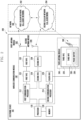
- Fig. 1 is a block diagram illustrating an electronic device 101 in a network environment 100 according to various embodiments.
- the electronic device 101 in the network environment 100 may communicate with an electronic device 102 via a first network 198 (e.g., a short-range wireless communication network), or at least one of an electronic device 104 or a server 108 via a second network 199 (e.g., a long-range wireless communication network).
- the electronic device 101 may communicate with the electronic device 104 via the server 108.
- the electronic device 101 may include a processor 120, memory 130, an input module 150, a sound output module 155, a display module 160, an audio module 170, a sensor module 176, an interface 177, a connecting terminal 178, a haptic module 179, a camera module 180, a power management module 188, a battery 189, a communication module 190, a subscriber identification module(SIM) 196, or an antenna module 197.
- at least one of the components e.g., the connecting terminal 178) may be omitted from the electronic device 101, or one or more other components may be added in the electronic device 101.
- some of the components e.g., the sensor module 176, the camera module 180, or the antenna module 197) may be implemented as a single component (e.g., the display module 160).
- the processor 120 may execute, for example, software (e.g., a program 140) to control at least one other component (e.g., a hardware or software component) of the electronic device 101 coupled with the processor 120, and may perform various data processing or computation. According to one embodiment, as at least part of the data processing or computation, the processor 120 may store a command or data received from another component (e.g., the sensor module 176 or the communication module 190) in volatile memory 132, process the command or the data stored in the volatile memory 132, and store resulting data in non-volatile memory 134.
- software e.g., a program 140
- the processor 120 may store a command or data received from another component (e.g., the sensor module 176 or the communication module 190) in volatile memory 132, process the command or the data stored in the volatile memory 132, and store resulting data in non-volatile memory 134.
- the processor 120 may include a main processor 121 (e.g., a central processing unit (CPU) or an application processor (AP)), or an auxiliary processor 123 (e.g., a graphics processing unit (GPU), a neural processing unit (NPU), an image signal processor (ISP), a sensor hub processor, or a communication processor (CP)) that is operable independently from, or in conjunction with, the main processor 121.
- a main processor 121 e.g., a central processing unit (CPU) or an application processor (AP)
- auxiliary processor 123 e.g., a graphics processing unit (GPU), a neural processing unit (NPU), an image signal processor (ISP), a sensor hub processor, or a communication processor (CP)
- the main processor 121 may be adapted to consume less power than the main processor 121, or to be specific to a specified function.
- the auxiliary processor 123 may be implemented as separate from, or as part of the main processor 121.
- the auxiliary processor 123 may control at least some of functions or states related to at least one component (e.g., the display module 160, the sensor module 176, or the communication module 190) among the components of the electronic device 101, instead of the main processor 121 while the main processor 121 is in an inactive (e.g., sleep) state, or together with the main processor 121 while the main processor 121 is in an active state (e.g., executing an application).
- the auxiliary processor 123 e.g., an image signal processor or a communication processor
- the auxiliary processor 123 may include a hardware structure specified for artificial intelligence model processing.
- An artificial intelligence model may be generated by machine learning. Such learning may be performed, e.g., by the electronic device 101 where the artificial intelligence is performed or via a separate server (e.g., the server 108). Learning algorithms may include, but are not limited to, e.g., supervised learning, unsupervised learning, semi-supervised learning, or reinforcement learning.
- the artificial intelligence model may include a plurality of artificial neural network layers.
- the artificial neural network may be a deep neural network (DNN), a convolutional neural network (CNN), a recurrent neural network (RNN), a restricted boltzmann machine (RBM), a deep belief network (DBN), a bidirectional recurrent deep neural network (BRDNN), deep Q-network or a combination of two or more thereof but is not limited thereto.
- the artificial intelligence model may, additionally or alternatively, include a software structure other than the hardware structure.
- the memory 130 may store various data used by at least one component (e.g., the processor 120 or the sensor module 176) of the electronic device 101.
- the various data may include, for example, software (e.g., the program 140) and input data or output data for a command related thererto.
- the memory 130 may include the volatile memory 132 or the non-volatile memory 134.
- the program 140 may be stored in the memory 130 as software, and may include, for example, an operating system (OS) 142, middleware 144, or an application 146.
- OS operating system
- middleware middleware
- application application
- the input module 150 may receive a command or data to be used by another component (e.g., the processor 120) of the electronic device 101, from the outside (e.g., a user) of the electronic device 101.
- the input module 150 may include, for example, a microphone, a mouse, a keyboard, a key (e.g., a button), or a digital pen (e.g., a stylus pen).
- the sound output module 155 may output sound signals to the outside of the electronic device 101.
- the sound output module 155 may include, for example, a speaker or a receiver.
- the speaker may be used for general purposes, such as playing multimedia or playing record.
- the receiver may be used for receiving incoming calls. According to an embodiment, the receiver may be implemented as separate from, or as part of the speaker.
- the display module 160 may visually provide information to the outside (e.g., a user) of the electronic device 101.
- the display module 160 may include, for example, a display, a hologram device, or a projector and control circuitry to control a corresponding one of the display, hologram device, and projector.
- the display module 160 may include a touch sensor adapted to detect a touch, or a pressure sensor adapted to measure the intensity of force incurred by the touch.
- the audio module 170 may convert a sound into an electrical signal and vice versa. According to an embodiment, the audio module 170 may obtain the sound via the input module 150, or output the sound via the sound output module 155 or a headphone of an external electronic device (e.g., an electronic device 102) directly (e.g., wiredly) or wirelessly coupled with the electronic device 101.
- an external electronic device e.g., an electronic device 102
- directly e.g., wiredly
- wirelessly e.g., wirelessly
- the sensor module 176 may detect an operational state (e.g., power or temperature) of the electronic device 101 or an environmental state (e.g., a state of a user) external to the electronic device 101, and then generate an electrical signal or data value corresponding to the detected state.
- the sensor module 176 may include, for example, a gesture sensor, a gyro sensor, an atmospheric pressure sensor, a magnetic sensor, an acceleration sensor, a grip sensor, a proximity sensor, a color sensor, an infrared (IR) sensor, a biometric sensor, a temperature sensor, a humidity sensor, or an illuminance sensor.
- the interface 177 may support one or more specified protocols to be used for the electronic device 101 to be coupled with the external electronic device (e.g., the electronic device 102) directly (e.g., wiredly) or wirelessly.
- the interface 177 may include, for example, a high definition multimedia interface (HDMI), a universal serial bus (USB) interface, a secure digital (SD) card interface, or an audio interface.
- HDMI high definition multimedia interface
- USB universal serial bus
- SD secure digital
- a connecting terminal 178 may include a connector via which the electronic device 101 may be physically connected with the external electronic device (e.g., the electronic device 102).
- the connecting terminal 178 may include, for example, a HDMI connector, a USB connector, a SD card connector, or an audio connector (e.g., a headphone connector).
- the haptic module 179 may convert an electrical signal into a mechanical stimulus (e.g., a vibration or a movement) or electrical stimulus which may be recognized by a user via his tactile sensation or kinesthetic sensation.
- the haptic module 179 may include, for example, a motor, a piezoelectric element, or an electric stimulator.
- the camera module 180 may capture a still image or moving images.
- the camera module 180 may include one or more lenses, image sensors, image signal processors, or flashes.
- the power management module 188 may manage power supplied to the electronic device 101.
- the power management module 188 may be implemented as at least part of, for example, a power management integrated circuit (PMIC).
- PMIC power management integrated circuit
- the battery 189 may supply power to at least one component of the electronic device 101.
- the battery 189 may include, for example, a primary cell which is not rechargeable, a secondary cell which is rechargeable, or a fuel cell.
- the communication module 190 may support establishing a direct (e.g., wired) communication channel or a wireless communication channel between the electronic device 101 and the external electronic device (e.g., the electronic device 102, the electronic device 104, or the server 108) and performing communication via the established communication channel.
- the communication module 190 may include one or more communication processors that are operable independently from the processor 120 (e.g., the application processor (AP)) and supports a direct (e.g., wired) communication or a wireless communication.
- AP application processor
- the communication module 190 may include a wireless communication module 192 (e.g., a cellular communication module, a short-range wireless communication module, or a global navigation satellite system (GNSS) communication module) or a wired communication module 194 (e.g., a local area network (LAN) communication module or a power line communication (PLC) module).
- a wireless communication module 192 e.g., a cellular communication module, a short-range wireless communication module, or a global navigation satellite system (GNSS) communication module
- GNSS global navigation satellite system
- wired communication module 194 e.g., a local area network (LAN) communication module or a power line communication (PLC) module.
- LAN local area network
- PLC power line communication
- a corresponding one of these communication modules may communicate with the external electronic device via the first network 198 (e.g., a short-range communication network, such as BluetoothTM, wireless-fidelity (Wi-Fi) direct, or infrared data association (IrDA)) or the second network 199 (e.g., a long-range communication network, such as a legacy cellular network, a 5G network, a next-generation communication network, the Internet, or a computer network (e.g., LAN or wide area network (WAN)).
- first network 198 e.g., a short-range communication network, such as BluetoothTM, wireless-fidelity (Wi-Fi) direct, or infrared data association (IrDA)
- the second network 199 e.g., a long-range communication network, such as a legacy cellular network, a 5G network, a next-generation communication network, the Internet, or a computer network (e.g., LAN or wide area network (WAN)).
- the wireless communication module 192 may identify and authenticate the electronic device 101 in a communication network, such as the first network 198 or the second network 199, using subscriber information (e.g., international mobile subscriber identity (IMSI)) stored in the subscriber identification module 196.
- subscriber information e.g., international mobile subscriber identity (IMSI)
- the wireless communication module 192 may support a 5G network, after a 4G network, and next-generation communication technology, e.g., new radio (NR) access technology.
- the NR access technology may support enhanced mobile broadband (eMBB), massive machine type communications (mMTC), or ultra-reliable and low-latency communications (URLLC).
- eMBB enhanced mobile broadband
- mMTC massive machine type communications
- URLLC ultra-reliable and low-latency communications
- the wireless communication module 192 may support a high-frequency band (e.g., the mmWave band) to achieve, e.g., a high data transmission rate.
- the wireless communication module 192 may support various technologies for securing performance on a high-frequency band, such as, e.g., beamforming, massive multiple-input and multiple-output (massive MIMO), full dimensional MIMO (FD-MIMO), array antenna, analog beam-forming, or large scale antenna.
- the wireless communication module 192 may support various requirements specified in the electronic device 101, an external electronic device (e.g., the electronic device 104), or a network system (e.g., the second network 199).
- the wireless communication module 192 may support a peak data rate (e.g., 20Gbps or more) for implementing eMBB, loss coverage (e.g., 164dB or less) for implementing mMTC, or U-plane latency (e.g., 0.5ms or less for each of downlink (DL) and uplink (LTL), or a round trip of 1ms or less) for implementing URLLC.
- a peak data rate e.g., 20Gbps or more
- loss coverage e.g., 164dB or less
- U-plane latency e.g., 0.5ms or less for each of downlink (DL) and uplink (LTL), or a round trip of 1ms or less
- the antenna module 197 may transmit or receive a signal or power to or from the outside (e.g., the external electronic device) of the electronic device 101.
- the antenna module 197 may include an antenna including a radiating element composed of a conductive material or a conductive pattern formed in or on a substrate (e.g., a printed circuit board (PCB)).
- the antenna module 197 may include a plurality of antennas (e.g., array antennas). In such a case, at least one antenna appropriate for a communication scheme used in the communication network, such as the first network 198 or the second network 199, may be selected, for example, by the communication module 190 (e.g., the wireless communication module 192) from the plurality of antennas.
- the signal or the power may then be transmitted or received between the communication module 190 and the external electronic device via the selected at least one antenna.
- another component e.g., a radio frequency integrated circuit (RFIC)
- RFIC radio frequency integrated circuit
- the antenna module 197 may form a mmWave antenna module.
- the mmWave antenna module may include a printed circuit board, a RFIC disposed on a first surface (e.g., the bottom surface) of the printed circuit board, or adjacent to the first surface and capable of supporting a designated high-frequency band (e.g., the mmWave band), and a plurality of antennas (e.g., array antennas) disposed on a second surface (e.g., the top or a side surface) of the printed circuit board, or adjacent to the second surface and capable of transmitting or receiving signals of the designated high-frequency band.
- a RFIC disposed on a first surface (e.g., the bottom surface) of the printed circuit board, or adjacent to the first surface and capable of supporting a designated high-frequency band (e.g., the mmWave band)
- a plurality of antennas e.g., array antennas
- At least some of the above-described components may be coupled mutually and communicate signals (e.g., commands or data) therebetween via an inter-peripheral communication scheme (e.g., a bus, general purpose input and output (GPIO), serial peripheral interface (SPI), or mobile industry processor interface (MIPI)).
- an inter-peripheral communication scheme e.g., a bus, general purpose input and output (GPIO), serial peripheral interface (SPI), or mobile industry processor interface (MIPI)
- commands or data may be transmitted or received between the electronic device 101 and the external electronic device 104 via the server 108 coupled with the second network 199.
- Each of the electronic devices 102 or 104 may be a device of a same type as, or a different type, from the electronic device 101.
- all or some of operations to be executed at the electronic device 101 may be executed at one or more of the external electronic devices 102, 104, or 108. For example, if the electronic device 101 should perform a function or a service automatically, or in response to a request from a user or another device, the electronic device 101, instead of, or in addition to, executing the function or the service, may request the one or more external electronic devices to perform at least part of the function or the service.
- the one or more external electronic devices receiving the request may perform the at least part of the function or the service requested, or an additional function or an additional service related to the request, and transfer an outcome of the performing to the electronic device 101.
- the electronic device 101 may provide the outcome, with or without further processing of the outcome, as at least part of a reply to the request.
- a cloud computing, distributed computing, mobile edge computing (MEC), or client-server computing technology may be used, for example.
- the electronic device 101 may provide ultra low-latency services using, e.g., distributed computing or mobile edge computing.
- the external electronic device 104 may include an internet-of-things (IoT) device.
- the server 108 may be an intelligent server using machine learning and/or a neural network.
- the external electronic device 104 or the server 108 may be included in the second network 199.
- the electronic device 101 may be applied to intelligent services (e.g., smart home, smart city, smart car, or healthcare) based on 5G communication technology or IoT-related technology.
- the electronic device may be one of various types of electronic devices.
- the electronic devices may include, for example, a portable communication device (e.g., a smartphone), a computer device, a portable multimedia device, a portable medical device, a camera, a wearable device, or a home appliance. According to an embodiment of the disclosure, the electronic devices are not limited to those described above.
- each of such phrases as “A or B,” “at least one of A and B,” “at least one of A or B,” “A, B, or C,” “at least one of A, B, and C,” and “at least one of A, B, or C,” may include any one of, or all possible combinations of the items enumerated together in a corresponding one of the phrases.
- such terms as “1st” and “2nd,” or “first” and “second” may be used to simply distinguish a corresponding component from another, and does not limit the components in other aspect (e.g., importance or order).
- an element e.g., a first element
- the element may be coupled with the other element directly (e.g., wiredly), wirelessly, or via a third element.
- module may include a unit implemented in hardware, software, or firmware, and may interchangeably be used with other terms, for example, “logic,” “logic block,” “part,” or “circuitry”.
- a module may be a single integral component, or a minimum unit or part thereof, adapted to perform one or more functions.
- the module may be implemented in a form of an application-specific integrated circuit (ASIC).
- ASIC application-specific integrated circuit
- Various embodiments as set forth herein may be implemented as software (e.g., the program 140) including one or more instructions that are stored in a storage medium (e.g., internal memory 136 or external memory 138) that is readable by a machine (e.g., the electronic device 101).
- a processor e.g., the processor 120
- the machine e.g., the electronic device 101
- the one or more instructions may include a code generated by a complier or a code executable by an interpreter.
- the machine-readable storage medium may be provided in the form of a non-transitory storage medium.
- non-transitory simply means that the storage medium is a tangible device, and does not include a signal (e.g., an electromagnetic wave), but this term does not differentiate between where data is semi-permanently stored in the storage medium and where the data is temporarily stored in the storage medium.
- a method may be included and provided in a computer program product.
- the computer program product may be traded as a product between a seller and a buyer.
- the computer program product may be distributed in the form of a machine-readable storage medium (e.g., compact disc read only memory (CD-ROM)), or be distributed (e.g., downloaded or uploaded) online via an application store (e.g., PlayStoreTM), or between two user devices (e.g., smart phones) directly. If distributed online, at least part of the computer program product may be temporarily generated or at least temporarily stored in the machine-readable storage medium, such as memory of the manufacturer's server, a server of the application store, or a relay server.
- CD-ROM compact disc read only memory
- an application store e.g., PlayStoreTM
- two user devices e.g., smart phones
- each component e.g., a module or a program of the above-described components may include a single entity or multiple entities, and some of the multiple entities may be separately disposed in different components. According to various embodiments, one or more of the above-described components may be omitted, or one or more other components may be added. Alternatively or additionally, a plurality of components (e.g., modules or programs) may be integrated into a single component. In such a case, according to various embodiments, the integrated component may still perform one or more functions of each of the plurality of components in the same or similar manner as they are performed by a corresponding one of the plurality of components before the integration.
- operations performed by the module, the program, or another component may be carried out sequentially, in parallel, repeatedly, or heuristically, or one or more of the operations may be executed in a different order or omitted, or one or more other operations may be added.
- FIG. 2 is a block diagram 200 of an electronic device 101 for supporting legacy network communication and 5G network communication according to various embodiments.
- the electronic device 101 may include a first communication processor 212, a second communication processor 214, a first radio frequency integrated circuit (RFIC) 222, a second RFIC 224, a third RFIC 226, a fourth RFIC 228, a first radio frequency front end (RFFE) 232, a second RFFE 234, a first antenna module 242, a second antenna module 244, and an antenna 248.
- the electronic device 101 may further include a processor 120 and a memory 130.
- a network 199 may include a first network 292 and a second network 294.
- the electronic device 101 may further include at least one among the components illustrated in FIG. 1 , and the network 199 may further include at least one other network.
- the first communication processor 212, the second communication processor 214, the first RFIC 222, the second RFIC 224, the fourth RFIC 228, the first RFFE 232, and the second RFFE 234 may form at least a part of a wireless communication module 192.
- the fourth RFIC 228 may be omitted or may be included as a part of the third RFIC 226.
- the first communication processor 212 may establish a communication channel for a band to be used for wireless communication with the first network 292, and may support legacy network communication through the established communication channel.
- the first network may be a legacy network including a 2 nd generation (2G), 3G, 4G, or long-term-evolution (LTE) network.
- the second communication processor 214 may establish a communication channel corresponding to a band (e.g., from about 6 GHz to about 60 GHz) designated among bands to be used for wireless communication with the second network 294, and may support 5G network communication through the established communication channel.
- the second network 294 may be a 5G network defined in the 3GPP.
- the first communication processor 212 or the second communication processor 214 may establish a communication channel corresponding to another designated band (e.g., about 6 GHz or less) among bands to be used for wireless communication with the second network 294, and may support 5G network communication through the established communication channel.
- the first communication processor 212 and the second communication processor 214 may be implemented in a single chip or a single package.
- the first communication processor 212 or the second communication processor 214 may be disposed in a single chip or a single package together with the processor 120, the auxiliary processor 123, or the communication module 190.
- the first RFIC 222 may convert a baseband signal generated by the first communication processor 212 into a radiofrequency (RF) signal of about 700 MHz to about 3 GHz used for the first network 292 (e.g., a legacy network).
- RF radiofrequency
- an RF signal may be acquired from the first network 292 (e.g., a legacy network) through an antenna (e.g., the first antenna module 242), and may be preprocessed through an RFFE (e.g., the first RFFE 232).
- the first RFIC 222 may convert the preprocessed RF signal into a baseband signal that can be processed by the first communication processor 212.
- the second RFIC 224 may convert a baseband signal generated by the first communication processor 212 or the second communication processor 214 into an RF signal (hereinafter, referred to as a "5G Sub6 RF signal") of a Sub6 band (e.g., about 6 GHz or less) used for the second network 294 (e.g., a 5G network).
- a 5G Sub6 RF signal may be acquired from the second network 294 (e.g., a 5G network) through an antenna (e.g., the second antenna module 244), and may be preprocessed through an RFFE (e.g., the second RFFE 234).
- the second RFIC 224 may convert the preprocessed 5G Sub6 RF signal into a baseband signal that can be processed by a corresponding communication processor among the first communication processor 212 or the second communication processor 214.
- the third RFIC 226 may convert a baseband signal generated by the second communication processor 214 into an RF signal (hereinafter, referred to as a "5G Above6 RF signal") of a 5G Above6 band (e.g., from about 6 GHz to about 60 GHz) to be used in the second network 294 (e.g., a 5G network).
- a 5G Above6 RF signal may be acquired from the second network 294 (e.g., a 5G network) through an antenna (e.g., the antenna 248), and may be preprocessed through the third RFFE 236.
- the third RFIC 226 may convert the preprocessed 5G Above6 RF signal into a baseband signal that can be processed by the second communication processor 214.
- the third RFFE 236 may be formed as a part of the third RFIC 226.
- the electronic device 101 may include the fourth RFIC 228 separately from the third RFIC 226 or as at least a part thereof.
- the fourth RFIC 228 may convert a baseband signal generated by the second communication processor 214 into an RF signal of an intermediate frequency band (e.g., from about 9 GHz to about 11 GHz) (hereinafter, referred to as an "IF signal"), and may then transmit the IF signal to the third RFIC 226.
- the third RFIC 226 may convert the IF signal into a 5G Above6 RF signal.
- a 5G Above6 RF signal may be received from the second network 294 (e.g., a 5G network) through an antenna (e.g., the antenna 248), and may be converted into an IF signal by the third RFIC 226.
- the fourth RFIC 228 may convert the IF signal into a baseband signal that can be processed by the second communication processor 2.
- the first RFIC 222 and the second RFIC 224 may be implemented as at least a part of a single package or a single chip.
- the first RFFE 232 and the second RFFE 234 may be implemented as at least a part of a single package or a single chip.
- at least one antenna module among the first antenna module 242 or the second antenna module 244 may be omitted, or may be combined with the other antenna module to process RF signals of multiple bands corresponding thereto.
- the third RFIC 226 and the antenna 248 may be arranged on the same substrate to form a third antenna module 246.
- the wireless communication module 192 or the processor 120 may be disposed on a first substrate (e.g., a main PCB).
- the third antenna module 246 may be formed by disposing the third RFIC 226 in a partial region (e.g., a lower surface) of a second substrate (e.g., a sub PCB) different from the first substrate and disposing the antenna 248 in another partial region (e.g., an upper surface) of the second substrate. Disposing the third RFIC 226 and the antenna 248 on the same substrate can reduce the length of a transmission line therebetween.
- the electronic device 101 can enhance the quality or speed of communication with the second network 294 (e.g., a 5G network).
- the second network 294 e.g., a 5G network
- the antenna 248 may be formed as an antenna array including multiple antenna elements which can be used for beamforming.
- the third RFIC 226 may include, as a part of the third RFFE 236, multiple phase shifters 238 corresponding to the multiple antenna elements.
- each of the multiple phase shifters 238 may shift the phase of a 5G Above6 RF signal to be transmitted from the electronic device 101 to the outside (e.g., a base station of a 5G network) through a corresponding antenna element.
- each of the multiple phase shifters 238 may shift the phase of a 5G Above6 RF signal received from the outside through a corresponding antenna element into an identical or substantially identical phase. This enables transmission or reception through beamforming between the electronic device 101 and the outside.
- the second network 294 may be operated independently of the first network 292 (e.g., a legacy network) (e.g., standalone (SA)) or may be operated while being connected to the first network (e.g., non-standalone (NSA)).
- the 5G network may include only an access network (e.g., a 5G radio access network (RAN) or a next-generation RAN (NG RAN)), and may not include a core network (e.g., a next-generation core (NGC) network).
- RAN radio access network
- NG RAN next-generation RAN
- the electronic device 101 may access the access network of the 5G network and may then access an external network (e.g., the Internet) under the control of a core network (e.g., an evolved packed core (EPC)) of the legacy network.
- EPC evolved packed core
- Protocol information e.g., LTE protocol information
- protocol information e.g., new radio (NR) protocol information
- NR new radio
- FIG. 3 is a block diagram illustrating the configuration of an electronic device 300 according to various embodiments.
- the electronic device 300 may include a first electronic component 310, a processor 320, a feeding unit 330, a ground 340, and a short pin 350.
- the first electronic component 310 may include a first bead 311, a first mounting unit 331, a first ground terminal 341, and a second ground terminal 342.
- the first electronic component 310 may include the first bead 311, a first switch 321, the first mounting unit 331, the first ground terminal 341, and the second ground terminal 342.
- the first electronic component 310 may be disposed in a front metal antenna of the electronic device 300.
- the first electronic component 310 may include at least one among a barometer, an ECG/Back key, a MIC, a power key, a speaker, and a UB FPCB.
- the first electronic component 310 may include any component which can be disposed on a FPCB of the front metal antenna, and is not limited to the above-described examples.
- the electronic device 300 may include the processor 320.
- the processor 320 is an element capable of controlling each element of the electronic device 300 and/or performing data processing or calculation regarding communication, and may include one or more processors 320.
- the processor 320 may include at least some of the elements and/or functions of the processor 120 in FIG. 1 .
- calculation and data processing functions which the processor 320 can implement in the electronic device 300, are not limited. However, hereinafter, a feature related to control of a switch device (e.g., the first switch 321 in FIG. 3 ) will be described in detail. Operations of the processor 320 may be performed by loading instructions stored in a memory (e.g., the memory 140 in FIG. 1 ).
- the electronic device 300 may include the feeding unit 330.
- the feeding unit 330 may include a portion for supplying a current to an antenna.
- An RF signal circuit is generated to transmit an RF signal from a main board of the electronic device 300 to the feeding unit 330.
- the main board may apply a ground to the short pin 350 to form a loop structure in the antenna together with the feeding unit 330.
- the ground 340 may include a ground, and the ground may provide a reference point of an operation of the first electronic component 310.
- the reference potential may be determined based on a main printed circuit board (PCB).
- the ground 340 may provide the reference potential to the feeding unit 330, the first electronic component 310, and the short pin 350.
- the feeding unit 330 may transmit an RF signal and a current toward the first mounting unit 331 disposed in the front metal antenna.
- the first mounting unit 331 may include a portion of the first electronic component 310, disposed nearby.
- the first ground terminal 341 and the second ground terminal 342 may be placed on the first electronic component 310, and may include portions for connecting the ground 340 to the first electronic component 310.
- the first switch 321 may be positioned at a side of the ground 340 to connect the ground 340 to the first ground terminal 341 or connect the ground 340 to the second ground terminal 342.
- the processor 320 may control an operation of the first switch 321.
- the electronic device 300 may include the first bead 311.
- the first bead 311 may function as an inductor or a filter in the electronic device 300. When an RF signal and a current flowing on a circuit pass through the first bead 311, the RF signal of a high-frequency band may be blocked. However, the first bead 311 may not have an effect on the operation of the first electronic component 310 by allowing a current used for an operation of the first electronic component 310 to pass therethrough. That is, the first bead 311 may play the role of blocking an RF signal of the antenna.
- the loop structure of the antenna may vary depending on the position of the first electronic component 310 with reference to the feeding unit 330.
- the loop structure may determine the structure, length, and resonance frequency of the antenna.
- the processor 320 may connect the first switch 321 to the first ground terminal 341 to perform control such that the first mounting unit 331 is connected to the ground 340 without going through the first bead 311. Further, the processor 320 may connect the first switch 321 to the second ground terminal 342 to perform control such that the first mounting unit 331 is connected to the ground 340 through the first bead 311.
- FIG. 4 illustrates the structure of an antenna of the electronic device 300 according to various embodiments.
- a loop is formed between the feeding unit 330 and the short pin 350.
- the length of an antenna may increase and relatively the band (frequency band) of the antenna may decrease.
- the length of the formed loop decreases, the length of the antenna may decrease and relatively the band of the antenna may increase.
- loop 1 is relatively long compared with loop 2.
- the relatively long loop 1 may be used as a low band antenna, and the relatively short loop 2 may be used as a high band antenna.
- a low band and a high band may imply a relative frequency range.
- a main board disposed in a metal housing 360 of the antenna may apply a path for passage of an RF signal to the feeding unit 330, and may apply a ground to the short pin 350.
- a switch may be positioned between the short pin 350 and the ground 340, and the switch may be in an electrically shorted state.
- the antenna may form a loop structure.
- the antenna may radiate an RF signal through the loop structure.
- the loop structure may be differently formed depending on the position of the short pin 350, and various loop structures may be formed by changing the arrangement position and the number of short pins 350 in the antenna.
- the antenna may have various lengths, and the radiation performance of the antenna for each band may be improved by adjusting the length of the antenna for each band.
- a first antenna for transmitting and receiving an RF signal of a relatively low band may include an antenna having a first length.
- a second antenna e.g., loop 2 for transmitting and receiving an RF signal of a relatively high band may include an antenna having a second length.
- the length of the antenna may be determined based on a frequency band (e.g., a high band or a low Band), and the first length of the first antenna taking charge of the low band may have a greater value than the second length of the second antenna taking charge of the high band.
- the performance of the antenna may be maximized for each frequency band by adjusting the length of the antenna. The adjustment of the length of the antenna according to loop formation will be described in detail in FIG. 9 .
- FIG. 5 illustrates electronic components disposed in an antenna of an electronic device according to various embodiments.
- the electronic device 300 may dispose one or more electronic components (e.g., 310A to 310D) in an antenna for operation.
- the first electronic component 310 may include the electronic components (e.g., 310A to 310D), and may include at least one among, for example, a barometer, an ECG/Back key, a MIC, a power key, a speaker, and a UB FPCB.
- the length of the antenna may be adjusted through arrangement of a short pin 350.
- short pins 350 connected according to bands may be adjusted or used together through a switch.
- the resonance shift width of the antenna may be variously formed by arranging multiple short pins 350 rather than using a single short pin 350.
- the performance of the antenna may be improved for each band.
- the first electronic component 310 may include at least one electronic component among a MIC, a speaker, a key button, a UB FPCB, a power key, and an ECG/back key.
- the first electronic component 310 may include the MIC.
- the MIC has a unique function (e.g., a function of amplifying a voice signal), and thus it may be difficult to remove the MIC and dispose the short pin 350. This may be true for other electronic components, including the speaker. As a result, it may be difficult to replace the first electronic component 310 with the short pin 350.
- the first electronic component 310 may be directly connected or coupled to the antenna and used as the short pin 350.
- the electronic device 300 may use the first electronic component 310 to operate the antenna like a multi-short pin 350 structure without further installing the short pin 350. It has been described above that the multi-short pin 350 structure may increase the resonance shift width of the antenna, and thus may have an effect of improving frequency performance in a specific band.
- the processor 320 may freely control open/short conditions through the switch.
- the first electronic component 310 when used as the short pin 350, the first electronic component 310 may be continuously in a shorted state or an open state. Therefore, it may be difficult to form the multi-short pin 350 structure of the antenna by using the first electronic component 310.
- FIG. 6 schematizes a situation in which multiple electronic components are disposed in the electronic device in FIG. 5 .
- the feeding unit 330 may include an electrically shorted state when a neighboring electronic component 310C or 310D is used to form a loop.
- the loop may be mainly formed between the feeding unit 330 and some electronic components 310C or 310D, and it may be difficult to use the remaining short pin 350 or the other electronic components 310A or 310B.
- the other electronic components 310A or 310B may include capacitor characteristics between a connection point and the ground 340. This may imply that the other electronic components is coupled and connected to the feeding unit 330 and not directly connected to the feeding unit 330.
- the first electronic component 310 may function as the ground 340 to form a loop with the feeding unit 330.
- the first electronic component 310 cannot itself perform open/short control, and thus it may be difficult to change a loop structure in the antenna. In this regard, it may be difficult for the antenna to perform resonance shifting. That is, the first electronic component 310 cannot perform control unlike a switch, and thus it may be difficult for the first electronic component 310 to be used together with the short pin 350 or as the short pin 350.
- FIG. 7 illustrates the inner structure of an electronic device in which a bead is further installed in FIG. 5 .
- the first bead 311 (bead) may be installed in the first electronic component 310.
- the first bead 311 may function as an inductor or a filter in the electronic device 300.
- an RF signal e.g., a high band signal or a low band signal
- a current flowing on a circuit pass through the first bead 311, the RF signal of a high-frequency band may be blocked.
- the first bead 311 may not have an effect on an operation of the first electronic component 310 by allowing a current used for the operation of the first electronic component 310 to pass therethrough. That is, the first bead 311 may play the role of blocking an RF signal of the antenna.
- the first bead 311 may make the first electronic component 310 be in an open state in which an RF signal cannot pass therethrough.
- FIG. 8 schematizes a situation in which multiple electronic components and a bead are disposed in the electronic device in FIG. 7 .
- the first electronic component 310 is continuously in an open state.
- the first electronic component 310 may not be an obstacle to forming a loop through the short pin 350.
- it may be difficult to form a loop of an antenna having a different band (frequency band). That is, as described in FIG.
- the antenna has no choice but to form a loop by using the short pin 350, and due to a limitation of the inner arrangement space, it may be difficult to freely install the short pin 350.
- the antenna may not variously form a loop, and it may be difficult to apply an optimal frequency capable of improving performance in each band.
- FIG. 9 illustrates a block diagram of a multi-short pin structure of an electronic device according to various embodiments.
- the electronic device 300 may include a first electronic component 310, a feeding unit 330, a short pin 350, and a second switch 322 for connecting the short pin 350 to the feeding unit 330.
- the first electronic component 310 may include a first mounting unit 331, a first bead 311, a first ground terminal 341, a second ground terminal 342, and a first switch 321.
- FIG. 9 illustrates a process of arranging the elements in FIG. 4 and changing an element connected to the feeding unit 330, depending on operations of the first switch 321 and the second switch 322.
- the first electronic component 310 may be connected, in a shorted state, to the feeding unit 330 depending on an operation of the first switch 321.
- the short pin 350 may be connected, in a shorted state, to the feeding unit 330 depending on an operation of the second switch 322.
- both the first electronic component 310 and the short pin 350 may be connected, in a shorted state, to the feeding unit 330 depending on operations of the first switch 321 and the second switch 322.
- points 901, 902, and 903 connected to the feeding unit 330 may vary depending on operations of the first switch 321 and the second switch 322.
- the processor 320 may control the first switch 321 and the second switch 322, thereby determining a point 901, 902, or 903 connected to the feeding unit 330.
- a description will be made assuming that the number of short pins 350 is one and the number of electronic component is one, but the disclosure is not limited thereto.
- the number of short pins 350 and the number of electronic components may be further increased, and accordingly the number of points connected to the feeding unit 330 may be increased.
- a loop may be formed at a point 902.
- the second switch for connecting the short pin 350 to the feeding unit 330 is opened, and when the first switch 321 of the first electronic component 310 is connected to the first ground terminal 341, a loop may be formed at a point 901.
- a loop may be formed at a point 903.
- the length of an antenna may be determined based on the distance between the feeding unit 330 and a point at which a loop is formed.
- the resonance frequency of the antenna may be determined based on the length of the antenna. For example, when a point connected to the feeding unit 330 corresponds to the point 902, the length of the antenna may be proportional to a length 920 between the feeding unit 330 and the point 902. Likewise, when a point connected to the feeding unit 330 corresponds to the point 901, the length of the antenna may be proportional to a length 910 between the feeding unit 330 and the point 901.
- the first switch 321 may connect the ground 340 to the first ground terminal 341, or may connect the ground 340 to the second ground terminal 342.
- the processor 320 may control an operation of the first switch 321 to determine a ground terminal connected to the ground 340.
- the first mounting unit 331 may be connected to the ground 340. A structure in which a current or a signal flows from the feeding unit 330 to the ground 340 through the first mounting unit 331, and the structure of the first switch 321 will be described in detail in FIGS. 12 and 13 .
- the second switch 322 may be positioned between the short pin 350 and the feeding unit 330.
- the processor 320 may control the short pin 350 and the feeding unit 330 to be connected to each other through the second switch 322.
- FIG. 10 shows, in a diagram and a circuit view, the structure of the electronic device in FIG. 9 .
- the processor 320 may control the first switch 321 and the second switch 322 to change a position in an antenna, at which connection to the feeding unit 330 is made. For example, when the processor 320 opens the first switch 321 and shorts the second switch 322, a position at which connection to the feeding unit 330 is made may vary depending on the position of the short pin 350. Alternatively, when the processor 320 shorts the first switch 321 and opens the second switch 322, a position at which connection to the feeding unit 330 is made may vary depending on the position of the first electronic component 310.
- a position at which connection to the feeding unit 330 is made may be determined between the first electronic component 310 and the short pin 350.
- the processor 320 opens both the first switch 321 and the second switch 322, the feeding unit 330 may not be connected to the ground 340. In this case, a loop structure of the antenna may not be formed, and thus the antenna may not radiate a signal.
- 1001 is a table in which results of the operations of the switches are arranged.
- the processor 320 may control opening/shorting of the first electronic component 310 by adding the first bead 311.
- At least four different loop paths may be formed through opening/shorting of the first electronic component 310 and opening/shorting of the short pin 350.
- This may vary depending on the number of electronic components and short pins, and even when there is a limitation in arranging short pins due to a spatial limitation, various loop paths may be formed by using the prearranged electronic components.
- the processor 320 may control the first switch 321 to be opened and the second switch 322 to be shorted.
- an antenna loop may be formed between the feeding unit 330 and the point 901 in FIG. 9 . This may correspond to an open/short case in table 1001 in FIG. 10 .
- the processor 320 may control the first switch 321 to be shorted and the second switch 322 to be opened. This may correspond to a short/open case in table 1001 in FIG. 10 .
- an antenna loop may be formed between the feeding unit 330 and the point 902 in FIG. 9 .
- the length of the antenna loop may include the first length 910.
- the length of the antenna loop may include the second length 920 longer than the first length 910.
- the processor 320 may control the first switch 321 and the second switch 322 such that antenna loops having different lengths are formed.
- the number of switches, the number of formable loops, the number of short pins, and the number of electronic components are not limited, and may vary depending on electronic devices .
- the number of formable loops may also be increased. As a result, the formation of various antenna loops may result in the improvement of frequency performance of an antenna.
- FIG. 11 illustrates multiple electronic components together in the structure of the electronic device in FIG. 10 .
- the electronic device 300 may further include multiple other electronic components in addition to the first electronic component 310.
- the first switch 321 may be formed between a first electronic component 310B and the feeding unit 330.
- the processor 320 may control opening/shorting of the first electronic component 310 through the first switch 321.
- a switch is not installed in multiple other electronic components (e.g., one of 310A, 310C, and 310D) other than one electronic component 310B.
- Switches may be added to the multiple other electronic components (e.g., one of 310A, 310C, and 310D) like one electronic component 310B, thereby variously forming points connected to the feeding unit 330 in the antenna.
- the inner structure of an electronic component for satisfying the following conditions will be described through FIGS. 12 and 13 below.
- FIG. 12 illustrates the inner structure of an electronic component disposed in an electronic device according to various embodiments.
- the first electronic component 310 may include a first mounting unit 331, a first ground terminal 341, a second ground terminal 342, and a first bead 311.
- the first ground terminal 341 and the second ground terminal 342 may be connected to the ground 340.
- the first switch 321 may be included between the first ground terminal 341, the second ground terminal 342, and the ground 340.
- the first bead 311 may be positioned between the first ground terminal 341 and the second ground terminal 342.
- the first bead 311 may be positioned between the second ground terminal 342 and the feeding unit 330. According to FIG.
- the first bead 311 may function as an inductor or a filter in the electronic device 300 or between the second ground terminal 342 and a mounting unit 331 of the first electronic component 310.
- the first bead 311 may not have an effect on an operation of the first electronic component 310 by allowing a current used for the operation of the first electronic component 310 to pass therethrough. That is, the first bead 311 may play the role of blocking an RF signal of an antenna.
- the first electronic component 310 may be connected to the ground 340 through the first ground terminal 341 and the second ground terminal 342.
- the processor 320 may connect the first ground terminal 341 to the ground 340 through the first switch 321.
- the first electronic component 310 may form a circuit with the feeding unit 330 to allow a current and an RF signal to flow, and form a loop structure of an antenna.
- the processor 320 may connect the second ground terminal 342 to the ground 340 through the first switch 321.
- the second ground terminal 342 may be connected to the first bead 311.
- the first bead 311 allows a current to pass therethrough, but may block an RF signal of a high band. The RF signal is blocked, and thus it is difficult to form a loop structure of an antenna.
- the processor 320 may control whether to allow RF signal to pass, while allowing a current used for the operation of the first electronic component 310 to flow to the first electronic component 310 through the first switch 321.
- FIG. 13 illustrates the inner structure and circuit of an electronic component disposed in an electronic device according to various embodiments.
- the first electronic component 310 may include a region 1310, in which the first mounting unit 331 disposed in an antenna is included, and a region 1320, in which the ground 340 and a circuit are formed.
- the processor 320 may connect the first ground terminal 341 to the ground 340, or may connect the second ground terminal 342 to the ground 340.
- a circuit 1301 by which a current and a signal flow from the feeding unit 330 to the ground 340 through the first mounting unit 331 may be formed.
- a circuit 1302 by which a current and a signal flow from the feeding unit 330 to the ground 340 through the first mounting unit 331 may be formed.
- the first bead 311 may be positioned between the second ground terminal 342 and the first mounting unit 331.
- a connection point, at which an antenna loop is formed, may be determined by selecting the circuit 1301 or 1302 through the first switch 321, and this process has been described in FIG. 10 .
- FIG. 14 is a block diagram illustrating the structure of an electronic device according to various embodiments.
- FIG. 14 additionally illustrates multiple electronic components, in addition to the first electronic component 310 in the block diagram of FIG. 9 .
- the processor 320 may control separate switches for connecting multiple electronic components to the ground 340.
- the processor 320 may variously determine, through the separate switches, points 1401 to 1404 at which the loop structure is formed.
- the points, at which the loop structure is formed are not limited thereto, and may vary depending on on/off of the separate switches and the number of electronic components.
- the resonance frequency of an antenna may be variously configured for each band by forming various loop structures. In this case, the performance of an antenna may be improved for each band. Further, the radiation performance of an antenna may be improved in an identical band. This will be described in detail in FIG. 15 .
- the electronic device 300 may further include a second electronic component.
- the second electronic component may include the same internal elements as the first electronic component 310 in FIG. 3 .
- the second electronic component may further include a second mounting unit (not shown) disposed near an antenna, a third ground terminal (not shown) and a fourth ground terminal (not shown) for selectively connecting a ground (e.g., the ground 340 in FIG. 3 ) to the second mounting unit (not shown), a third switch (not shown) positioned at a ground side so as to selectively connect the ground to the third ground terminal (not shown) or the fourth ground terminal (not shown), and a second bead (not shown) positioned between the fourth ground terminal (not shown) and the second mounting unit (not shown).
- a ground e.g., the ground 340 in FIG. 3
- a third switch not shown
- a second bead not shown
- the processor 320 may connect the third switch (not shown) to the third ground terminal (not shown) to perform control such that the second mounting unit (not shown) and the ground 340 is connected to each other without going through the second bead (not shown).
- the processor 320 may connect the third switch (not shown) to the fourth ground terminal (not shown) to perform control such that the second mounting unit (not shown) is connected to the ground 340 through the second bead (not shown).
- the processor 320 may connect the first switch 321 to the first ground terminal 341 to perform control such that a current and an RF signal supplied to the first electronic component 310 are electrically connected, or may connect the first switch 321 to the second ground terminal 342 to perform control such that a current supplied to the first electronic component 310 flows but an RF signal is not transmitted. Further, the processor 320 may connect the third switch (not shown) to the third ground terminal (not shown) to perform control such that a current and an RF signal, supplied to the second electronic component, are electrically connected, or may connect the third switch (not shown) to the fourth ground terminal (not shown) to perform control such that a current supplied to the second electronic component flows but an RF signal is not transmitted.
- an electronic device may include a feeding unit (e.g., the feeding unit 330 in FIG. 3 ) configured to be provided with a feeding signal from a communication circuit of the electronic device, a first electronic component (e.g., the first electronic component 310 in FIG. 3 ) disposed in the electronic device, a first mounting unit (e.g., the first mounting unit 331 in FIG. 3 ) including a portion of the first electronic component, disposed in an antenna, a ground (e.g., the ground 340 in FIG.
- a feeding unit e.g., the feeding unit 330 in FIG. 3
- a first electronic component e.g., the first electronic component 310 in FIG. 3
- a first mounting unit e.g., the first mounting unit 331 in FIG. 3
- a ground e.g., the ground 340 in FIG.
- the feeding unit may apply an RF signal by using the first mounting unit disposed in the electronic component.
- the electronic device may further include a second mounting unit of a second electronic component disposed in the antenna, a third ground terminal and a fourth ground terminal configured to electrically connect the ground to the second mounting unit, a second switch positioned at a side of the ground to selectively electrically connect the ground to the third ground terminal or the fourth ground terminal, and a second bead positioned between the fourth ground terminal and the second mounting unit.
- a processor may electrically connect the second switch to the third ground terminal to perform control such that the second mounting unit is electrically connected to the ground without going through the second bead, or may electrically connect the second switch to the fourth ground terminal to perform control such that the second mounting unit is electrically connected to the ground through the second bead.
- the processor may electrically connect the first switch to the first ground terminal to perform control such that an RF signal is applied through the first electronic component, and may electrically connect the second switch to the fourth ground terminal to perform control such that an RF signal is not applied.
- the processor may electrically connect the first switch to the second ground terminal to perform control such that an RF signal is not applied through the first electronic component, and may electrically connect the second switch to the third ground terminal to perform control such that an RF signal is applied through the second electronic component.
- the processor may electrically connect the first switch to the second ground terminal to perform control such that an RF signal is not applied through the first electronic component, and may electrically connect the second switch to the fourth ground terminal to perform control such that an RF signal is not applied through the second electronic component.
- the processor may electrically connect the first switch to the first ground terminal to perform control such that an RF signal is applied through the first electronic component, and may electrically connect the second switch to the third ground terminal to perform control such that an RF signal is applied through the second electronic component.
- the first electronic component and the second electronic component may include at least one among a barometer, an ECG/Back key, a MIC, a power key, a speaker, and a UB FPCB.
- the electronic device may further include a short pin (e.g., the short pin 350 in FIG. 3 ) positioned in the antenna, and a third switch configured to electrically connect the short pin to the feeding unit, wherein the short pin is positioned in a third direction that is different from a first direction and a second direction of the feeding unit, and the processor may control on/off of the third switch.
- a short pin e.g., the short pin 350 in FIG. 3
- the processor may control on/off of the third switch.
- the processor may electrically connect the first switch to the first ground terminal to perform control such that an RF signal is applied through the first electronic component or electrically connect the first switch to the second ground terminal to perform control such that an RF signal is not applied through the first electronic component, may electrically connect the second switch to the third ground terminal to perform control such that an RF signal is applied through the second electronic component or electrically connect the second switch to the fourth ground terminal to perform control such that an RF signal is not applied through the second electronic component, and may control the third switch (e.g., the switch in FIG. 4 ) to be opened or shorted.
- the third switch e.g., the switch in FIG. 4
- the short pin may be positioned in a second direction different from the first direction of the feeding unit, and the processor may control on/off of the second switch.
- the processor may electrically connect the first switch to the first ground terminal to perform control such that a current and an RF signal are applied through the first electronic component, and may control the second switch to be opened.
- the processor may electrically connect the first switch to the second ground terminal to perform control such that an RF signal is not applied, and may control the second switch to be shorted.
- the processor may electrically connect the first switch to the second ground terminal to perform control such that an RF signal is not applied through the first electronic component, and may control the second switch to be opened.
- the processor may electrically connect the first switch to the first ground terminal to perform control such that an RF signal is applied through the first electronic component, and may control the second switch to be shorted.
- FIG. 15 is a graph showing frequency-specific performance of an antenna of an electronic device according to various embodiments.
- the x-axis may indicate the frequency of an antenna.
- the y-axis may indicate the performance of the antenna according to the frequency. It may be understood that the higher the value of the y-axis is, the better the antenna performance in a corresponding frequency domain is.
- the frequency domain of the antenna may include domains B5 and B8, which are relatively low bands, and domains BT and B7, which are relatively high bands.
- Line 1501 may indicate the case in which a loop is formed through the first electronic component 310 by shorting the first switch 321 (for example, connecting the first ground terminal 341 to the ground 340) and opening the second switch 322.
- Line 1502 may indicate the case in which a loop is formed through the short pin 350 by opening the first switch 321 (for example, connecting the second ground terminal 342 to the ground 340) and shorting the second switch 322.
- Line 1503 may indicate the case in which a loop is formed through a point between the first electronic component 310 and the short pin 350 by shorting the first switch 321 and shoring the second switch 322.
- the highest point is formed at about 800 MHz, but, in line 1501, the highest point is formed at about 900 MHz.
- the highest point may include a point at which the performance of a band is maximized within domains B5 and B8.
- the processor 320 may open the first switch 321 and short the second switch 322, thereby maximally improving the performance of the antenna.
- the processor 320 may short the first switch 321 and open the second switch 322, thereby maximally improving the performance of the antenna.
- the processor 320 may also adjust a switch on the same principle in other bands, thereby maximally improving the performance of the antenna.
- domain BT which is a high-band frequency domain of the antenna
- line 1501 in which an antenna loop is formed through the first electronic component 310
- line 1502 in which an antenna loop is formed through the short pin 350.
- the higher the line is positioned on the graph the more improved the performance of the antenna is.
- using the first electronic component 310 as a type of short pin 350 may improve the band-specific performance of the antenna compared with using only the short pin 350.
- the electronic device in a method for improving the performance of an antenna of an electronic device, may include a feeding unit (e.g., the feeding unit 330 in FIG. 3 ) configured to be provided with a feeding signal from a communication circuit of the electronic device, a first electronic component (e.g., the first electronic component 310 in FIG. 3 ) disposed in the electronic device, a first mounting unit (e.g., the first mounting unit 331 in FIG. 3 ) including a portion of the first electronic component, disposed in the antenna, a ground (e.g., the ground 340 in FIG.
- a feeding unit e.g., the feeding unit 330 in FIG. 3
- a first electronic component e.g., the first electronic component 310 in FIG. 3
- a first mounting unit e.g., the first mounting unit 331 in FIG. 3
- a ground e.g., the ground 340 in FIG.
- first ground terminal configured to provide a reference potential to the feeding unit
- first ground terminal and a second ground terminal configured to electrically connect the ground to the first mounting unit
- a first bead e.g., the first bead 311 in FIG. 3
- a first switch e.g., the first switch 321 in FIG. 3
- the first switch positioned at a side of the ground to electrically connect the ground to at least one of the first ground terminal (e.g., the first ground terminal 341 in FIG. 3 ) or the second ground terminal (e.g., the second ground terminal 342 in FIG. 3 ).
- the method for improving the performance of the antenna of the electronic device may include an operation of electrically connect the first switch to the first ground terminal to perform control such that the first mounting unit is electrically connected to the ground without going through the first bead, or an operation of electrically connecting the first switch to the second ground terminal to perform control such that the first mounting unit is electrically connected to the ground through the first bead.
- the electronic device may further include a second mounting unit of a second electronic component disposed in the antenna, a third ground terminal and a fourth ground terminal configured to electrically connect the ground to the second mounting unit, a second switch positioned at a side of the ground to selectively electrically connect the ground to the third ground terminal or the fourth ground terminal, and a second bead positioned between the fourth ground terminal and the second mounting unit.
- the method of improving the performance of the antenna of the electronic device may further include an operation of electrically connecting the second switch to the third ground terminal to perform control such that the second mounting unit is electrically connected to the ground without going through the second bead, or an operation of electrically connecting the second switch to the fourth ground terminal to perform control such that the second mounting unit is electrically connected to the ground through the second bead.
- the electronic device may further include a short pin (e.g., the short pin 350 in FIG. 3 ) positioned on a flexible printed circuit board (FPCB) of the antenna, and a second switch configured to electrically connect the short pin to the feeding unit.
- the method of improving the performance of the antenna of the electronic device may further include an operation of connecting the first switch to the first ground terminal to perform control such that an RF signal is applied through the first electronic component and opening the second switch, or an operation of connecting the first switch to the second ground terminal to perform control such that an RF signal is not applied through the first electronic component and shorting the second switch.
- the electronic device may further include a short pin and a third switch configured to electrically connect the short pin to the feeding unit.
- the method of improving the performance of the antenna of the electronic device may further include an operation of connecting the first switch to the first ground terminal to perform control such that an RF signal is applied through the first electronic component, or connecting the first switch to the second ground terminal to perform control such that an RF signal is not applied through the first electronic component, an operation of connecting the second switch to the third ground terminal to perform control such that an RF signal is applied through the second electronic component or connecting the second switch to the fourth ground terminal to perform control such that an RF signal is not applied through the second electronic component, and an operation of opening the third switch to electrically disconnect the feeding unit from the short pin or shorting the third switch to electrically connect the feeding unit to the short pin.
- the first electronic component and the second electronic component may include at least one among a barometer, an ECG/Back key, a MIC, a power key, a speaker, and a UB FPCB.
Abstract
An electronic device according to various embodiments may comprise: a power feeding portion which receives a power feeding signal from a communication circuit of the electronic device; an antenna electrically connected to the power feeding portion; a first electronic component disposed inside the electronic device; a first mounting portion which is in a first direction of the power feeding portion and includes a portion of the first electronic component disposed near an antenna; a grounding portion which provides a reference potential for the power feeding portion; a first ground terminal and a second ground terminal which are located on the first electronic component, and are included in a circuit electrically connecting the grounding portion to the first electronic component; a first bead located between the second ground terminal and the first mounting portion; a first switch which is located at the grounding portion and electrically connects the grounding portion to the first ground terminal or electrically connects the grounding portion to the second ground terminal; and a processor which controls the operation of the first switch. The processor may control to electrically connect the first switch to the first ground terminal such that the first mounting portion is electrically connected to the grounding portion without passing through the first bead or may control to electrically connect the first switch to the second ground terminal such that the first mounting portion is electrically connected to the grounding portion by passing through the first bead.
Description
- Various embodiments of the disclosure relate to an electronic device and may include, for example, an electronic device including an antenna and a method for improving antenna performance of an electronic device.
- An electronic device may have a front metal housing used to form a loop structure of an antenna that supports frequency bands of 3G, LTE, 5G, and/or GPS. A front metal loop antenna may include a metal housing, a feeding unit, and/or a short pin. The feeding unit and the short pin may be connected through a c-clip, and may be directly connected to the metal housing through a metal pad.
- For example, the electronic device may apply a path to the feeding unit such at an RF signal can move, and may apply a ground to the short pin. In this case, a loop may be formed between the feeding unit and the short pin. The band frequency of the antenna may vary depending on the loop structure formed inside the antenna. A changed position of the short pin may vary the loop structure. In this case, the band frequency of the antenna may also vary. Eventually, the position of the short pin may be controlled to control the band frequency of the antenna.
- An electronic device which is lightweight, flat, short, and compact has a limited internal disposition space, which may make installation of an additional short pin difficult. Without an additional short pin, it may be difficult to variously form the antenna band frequency. In this case, the band frequency supported by the electronic device may be restricted.
- Addition of a short pin may require an increased antenna size, and this may make it difficult to make the electronic device compact. Various embodiments disclosed herein may provide an antenna supporting various band frequencies without an additional short pin.
- An electronic device according to various embodiments may include a feeding unit configured to be provided with a feeding signal from a communication circuit of the electronic device, an antenna electrically connected to the feeding unit, a first electronic component disposed in the electronic device, a first mounting unit positioned in a first direction of the feeding unit and including a portion of the first electronic component, disposed near the antenna, a ground configured to provide a reference potential to the feeding unit, a first ground terminal and a second ground terminal, positioned on the first electronic component and included in a circuit configured to electrically connect the ground to the first electronic component, a first bead positioned between the second ground terminal and the first mounting unit, a first switch positioned at a side of the ground to electrically connect the ground to the first ground terminal or electrically connect the ground to the second ground terminal, and a processor configured to control an operation of the first switch. The processor may electrically connect the first switch to the first ground terminal to perform control such that the first mounting unit is electrically connected to the ground without going through the first bead, or electrically connect the first switch to the second ground terminal to perform control such that the first mounting unit is electrically connected to the ground through the first bead.
- A method for improving performance of an antenna of an electronic device according to various embodiments may include electrically connecting a first switch to a first ground terminal to perform control such that a first mounting unit is electrically connected to a ground without going through the a bead, or electrically connecting the first switch to a second ground terminal to perform control such that the first mounting unit is electrically connected to the ground through the first bead.
- An electronic device and a method for improving antenna performance of an electronic device, according to the disclosure, may improve the antenna performance through an internal electronic component without an additional short pin.
- According to various embodiments, antenna performance may be improved without an additional short pin, thereby making the antenna and the electronic device compact.
-
-
FIG. 1 is a block diagram of an electronic device in a network environment according to various embodiments; -
FIG. 2 is a block diagram of an electronic device for supporting legacy network communication and 5G network communication according to various embodiments; -
FIG. 3 is a block diagram illustrating the configuration of an electronic device according to various embodiments; -
FIG. 4 illustrates the structure of an antenna of an electronic device according to various embodiments; -
FIG. 5 illustrates electronic components disposed in an antenna of an electronic device according to various embodiments; -
FIG. 6 schematizes a situation in which multiple electronic components are disposed in the electronic device inFIG. 5 ; -
FIG. 7 illustrates the inner structure of an electronic device in which a bead is further installed inFIG. 5 ; -
FIG. 8 schematizes a situation in which multiple electronic components and a bead are disposed in the electronic device inFIG. 7 . -
FIG. 9 illustrates a block diagram of a multi-short pin structure of an electronic device according to various embodiments; -
FIG. 10 shows, in a diagram and a circuit view, the structure of the electronic device inFIG. 9 ; -
FIG. 11 illustrates multiple electronic components together in the structure of the electronic device inFIG. 10 ; -
FIG. 12 illustrates the inner structure of an electronic component disposed in an electronic device according to various embodiments; -
FIG. 13 illustrates the inner structure and circuit of an electronic component disposed in an electronic device according to various embodiments; -
FIG. 14 is a block diagram illustrating the structure of an electronic device according to various embodiments; and -
FIG. 15 is a graph showing frequency-specific performance of an antenna of an electronic device according to various embodiments. -
Fig. 1 is a block diagram illustrating anelectronic device 101 in anetwork environment 100 according to various embodiments. Referring toFig. 1 , theelectronic device 101 in thenetwork environment 100 may communicate with anelectronic device 102 via a first network 198 (e.g., a short-range wireless communication network), or at least one of anelectronic device 104 or aserver 108 via a second network 199 (e.g., a long-range wireless communication network). According to an embodiment, theelectronic device 101 may communicate with theelectronic device 104 via theserver 108. According to an embodiment, theelectronic device 101 may include aprocessor 120,memory 130, aninput module 150, asound output module 155, adisplay module 160, anaudio module 170, asensor module 176, aninterface 177, aconnecting terminal 178, ahaptic module 179, acamera module 180, apower management module 188, abattery 189, acommunication module 190, a subscriber identification module(SIM) 196, or anantenna module 197. In some embodiments, at least one of the components (e.g., the connecting terminal 178) may be omitted from theelectronic device 101, or one or more other components may be added in theelectronic device 101. In some embodiments, some of the components (e.g., thesensor module 176, thecamera module 180, or the antenna module 197) may be implemented as a single component (e.g., the display module 160). - The
processor 120 may execute, for example, software (e.g., a program 140) to control at least one other component (e.g., a hardware or software component) of theelectronic device 101 coupled with theprocessor 120, and may perform various data processing or computation. According to one embodiment, as at least part of the data processing or computation, theprocessor 120 may store a command or data received from another component (e.g., thesensor module 176 or the communication module 190) involatile memory 132, process the command or the data stored in thevolatile memory 132, and store resulting data innon-volatile memory 134. According to an embodiment, theprocessor 120 may include a main processor 121 (e.g., a central processing unit (CPU) or an application processor (AP)), or an auxiliary processor 123 (e.g., a graphics processing unit (GPU), a neural processing unit (NPU), an image signal processor (ISP), a sensor hub processor, or a communication processor (CP)) that is operable independently from, or in conjunction with, themain processor 121. For example, when theelectronic device 101 includes themain processor 121 and theauxiliary processor 123, theauxiliary processor 123 may be adapted to consume less power than themain processor 121, or to be specific to a specified function. Theauxiliary processor 123 may be implemented as separate from, or as part of themain processor 121. - The
auxiliary processor 123 may control at least some of functions or states related to at least one component (e.g., thedisplay module 160, thesensor module 176, or the communication module 190) among the components of theelectronic device 101, instead of themain processor 121 while themain processor 121 is in an inactive (e.g., sleep) state, or together with themain processor 121 while themain processor 121 is in an active state (e.g., executing an application). According to an embodiment, the auxiliary processor 123 (e.g., an image signal processor or a communication processor) may be implemented as part of another component (e.g., thecamera module 180 or the communication module 190) functionally related to theauxiliary processor 123. According to an embodiment, the auxiliary processor 123 (e.g., the neural processing unit) may include a hardware structure specified for artificial intelligence model processing. An artificial intelligence model may be generated by machine learning. Such learning may be performed, e.g., by theelectronic device 101 where the artificial intelligence is performed or via a separate server (e.g., the server 108). Learning algorithms may include, but are not limited to, e.g., supervised learning, unsupervised learning, semi-supervised learning, or reinforcement learning. The artificial intelligence model may include a plurality of artificial neural network layers. The artificial neural network may be a deep neural network (DNN), a convolutional neural network (CNN), a recurrent neural network (RNN), a restricted boltzmann machine (RBM), a deep belief network (DBN), a bidirectional recurrent deep neural network (BRDNN), deep Q-network or a combination of two or more thereof but is not limited thereto. The artificial intelligence model may, additionally or alternatively, include a software structure other than the hardware structure. - The
memory 130 may store various data used by at least one component (e.g., theprocessor 120 or the sensor module 176) of theelectronic device 101. The various data may include, for example, software (e.g., the program 140) and input data or output data for a command related thererto. Thememory 130 may include thevolatile memory 132 or thenon-volatile memory 134. - The
program 140 may be stored in thememory 130 as software, and may include, for example, an operating system (OS) 142,middleware 144, or anapplication 146. - The
input module 150 may receive a command or data to be used by another component (e.g., the processor 120) of theelectronic device 101, from the outside (e.g., a user) of theelectronic device 101. Theinput module 150 may include, for example, a microphone, a mouse, a keyboard, a key (e.g., a button), or a digital pen (e.g., a stylus pen). - The
sound output module 155 may output sound signals to the outside of theelectronic device 101. Thesound output module 155 may include, for example, a speaker or a receiver. The speaker may be used for general purposes, such as playing multimedia or playing record. The receiver may be used for receiving incoming calls. According to an embodiment, the receiver may be implemented as separate from, or as part of the speaker. - The
display module 160 may visually provide information to the outside (e.g., a user) of theelectronic device 101. Thedisplay module 160 may include, for example, a display, a hologram device, or a projector and control circuitry to control a corresponding one of the display, hologram device, and projector. According to an embodiment, thedisplay module 160 may include a touch sensor adapted to detect a touch, or a pressure sensor adapted to measure the intensity of force incurred by the touch. - The
audio module 170 may convert a sound into an electrical signal and vice versa. According to an embodiment, theaudio module 170 may obtain the sound via theinput module 150, or output the sound via thesound output module 155 or a headphone of an external electronic device (e.g., an electronic device 102) directly (e.g., wiredly) or wirelessly coupled with theelectronic device 101. - The
sensor module 176 may detect an operational state (e.g., power or temperature) of theelectronic device 101 or an environmental state (e.g., a state of a user) external to theelectronic device 101, and then generate an electrical signal or data value corresponding to the detected state. According to an embodiment, thesensor module 176 may include, for example, a gesture sensor, a gyro sensor, an atmospheric pressure sensor, a magnetic sensor, an acceleration sensor, a grip sensor, a proximity sensor, a color sensor, an infrared (IR) sensor, a biometric sensor, a temperature sensor, a humidity sensor, or an illuminance sensor. - The
interface 177 may support one or more specified protocols to be used for theelectronic device 101 to be coupled with the external electronic device (e.g., the electronic device 102) directly (e.g., wiredly) or wirelessly. According to an embodiment, theinterface 177 may include, for example, a high definition multimedia interface (HDMI), a universal serial bus (USB) interface, a secure digital (SD) card interface, or an audio interface. - A connecting
terminal 178 may include a connector via which theelectronic device 101 may be physically connected with the external electronic device (e.g., the electronic device 102). According to an embodiment, the connectingterminal 178 may include, for example, a HDMI connector, a USB connector, a SD card connector, or an audio connector (e.g., a headphone connector). - The
haptic module 179 may convert an electrical signal into a mechanical stimulus (e.g., a vibration or a movement) or electrical stimulus which may be recognized by a user via his tactile sensation or kinesthetic sensation. According to an embodiment, thehaptic module 179 may include, for example, a motor, a piezoelectric element, or an electric stimulator. - The
camera module 180 may capture a still image or moving images. According to an embodiment, thecamera module 180 may include one or more lenses, image sensors, image signal processors, or flashes. - The
power management module 188 may manage power supplied to theelectronic device 101. According to one embodiment, thepower management module 188 may be implemented as at least part of, for example, a power management integrated circuit (PMIC). - The
battery 189 may supply power to at least one component of theelectronic device 101. According to an embodiment, thebattery 189 may include, for example, a primary cell which is not rechargeable, a secondary cell which is rechargeable, or a fuel cell. - The
communication module 190 may support establishing a direct (e.g., wired) communication channel or a wireless communication channel between theelectronic device 101 and the external electronic device (e.g., theelectronic device 102, theelectronic device 104, or the server 108) and performing communication via the established communication channel. Thecommunication module 190 may include one or more communication processors that are operable independently from the processor 120 (e.g., the application processor (AP)) and supports a direct (e.g., wired) communication or a wireless communication. According to an embodiment, thecommunication module 190 may include a wireless communication module 192 (e.g., a cellular communication module, a short-range wireless communication module, or a global navigation satellite system (GNSS) communication module) or a wired communication module 194 (e.g., a local area network (LAN) communication module or a power line communication (PLC) module). A corresponding one of these communication modules may communicate with the external electronic device via the first network 198 (e.g., a short-range communication network, such as BluetoothTM, wireless-fidelity (Wi-Fi) direct, or infrared data association (IrDA)) or the second network 199 (e.g., a long-range communication network, such as a legacy cellular network, a 5G network, a next-generation communication network, the Internet, or a computer network (e.g., LAN or wide area network (WAN)). These various types of communication modules may be implemented as a single component (e.g., a single chip), or may be implemented as multi components (e.g., multi chips) separate from each other. Thewireless communication module 192 may identify and authenticate theelectronic device 101 in a communication network, such as thefirst network 198 or thesecond network 199, using subscriber information (e.g., international mobile subscriber identity (IMSI)) stored in thesubscriber identification module 196. - The
wireless communication module 192 may support a 5G network, after a 4G network, and next-generation communication technology, e.g., new radio (NR) access technology. The NR access technology may support enhanced mobile broadband (eMBB), massive machine type communications (mMTC), or ultra-reliable and low-latency communications (URLLC). Thewireless communication module 192 may support a high-frequency band (e.g., the mmWave band) to achieve, e.g., a high data transmission rate. Thewireless communication module 192 may support various technologies for securing performance on a high-frequency band, such as, e.g., beamforming, massive multiple-input and multiple-output (massive MIMO), full dimensional MIMO (FD-MIMO), array antenna, analog beam-forming, or large scale antenna. Thewireless communication module 192 may support various requirements specified in theelectronic device 101, an external electronic device (e.g., the electronic device 104), or a network system (e.g., the second network 199). According to an embodiment, thewireless communication module 192 may support a peak data rate (e.g., 20Gbps or more) for implementing eMBB, loss coverage (e.g., 164dB or less) for implementing mMTC, or U-plane latency (e.g., 0.5ms or less for each of downlink (DL) and uplink (LTL), or a round trip of 1ms or less) for implementing URLLC. - The
antenna module 197 may transmit or receive a signal or power to or from the outside (e.g., the external electronic device) of theelectronic device 101. According to an embodiment, theantenna module 197 may include an antenna including a radiating element composed of a conductive material or a conductive pattern formed in or on a substrate (e.g., a printed circuit board (PCB)). According to an embodiment, theantenna module 197 may include a plurality of antennas (e.g., array antennas). In such a case, at least one antenna appropriate for a communication scheme used in the communication network, such as thefirst network 198 or thesecond network 199, may be selected, for example, by the communication module 190 (e.g., the wireless communication module 192) from the plurality of antennas. The signal or the power may then be transmitted or received between thecommunication module 190 and the external electronic device via the selected at least one antenna. According to an embodiment, another component (e.g., a radio frequency integrated circuit (RFIC)) other than the radiating element may be additionally formed as part of theantenna module 197. - According to various embodiments, the
antenna module 197 may form a mmWave antenna module. According to an embodiment, the mmWave antenna module may include a printed circuit board, a RFIC disposed on a first surface (e.g., the bottom surface) of the printed circuit board, or adjacent to the first surface and capable of supporting a designated high-frequency band (e.g., the mmWave band), and a plurality of antennas (e.g., array antennas) disposed on a second surface (e.g., the top or a side surface) of the printed circuit board, or adjacent to the second surface and capable of transmitting or receiving signals of the designated high-frequency band. - At least some of the above-described components may be coupled mutually and communicate signals (e.g., commands or data) therebetween via an inter-peripheral communication scheme (e.g., a bus, general purpose input and output (GPIO), serial peripheral interface (SPI), or mobile industry processor interface (MIPI)).
- According to an embodiment, commands or data may be transmitted or received between the
electronic device 101 and the externalelectronic device 104 via theserver 108 coupled with thesecond network 199. Each of theelectronic devices electronic device 101. According to an embodiment, all or some of operations to be executed at theelectronic device 101 may be executed at one or more of the externalelectronic devices electronic device 101 should perform a function or a service automatically, or in response to a request from a user or another device, theelectronic device 101, instead of, or in addition to, executing the function or the service, may request the one or more external electronic devices to perform at least part of the function or the service. The one or more external electronic devices receiving the request may perform the at least part of the function or the service requested, or an additional function or an additional service related to the request, and transfer an outcome of the performing to theelectronic device 101. Theelectronic device 101 may provide the outcome, with or without further processing of the outcome, as at least part of a reply to the request. To that end, a cloud computing, distributed computing, mobile edge computing (MEC), or client-server computing technology may be used, for example. Theelectronic device 101 may provide ultra low-latency services using, e.g., distributed computing or mobile edge computing. In another embodiment, the externalelectronic device 104 may include an internet-of-things (IoT) device. Theserver 108 may be an intelligent server using machine learning and/or a neural network. According to an embodiment, the externalelectronic device 104 or theserver 108 may be included in thesecond network 199. Theelectronic device 101 may be applied to intelligent services (e.g., smart home, smart city, smart car, or healthcare) based on 5G communication technology or IoT-related technology. - The electronic device according to various embodiments may be one of various types of electronic devices. The electronic devices may include, for example, a portable communication device (e.g., a smartphone), a computer device, a portable multimedia device, a portable medical device, a camera, a wearable device, or a home appliance. According to an embodiment of the disclosure, the electronic devices are not limited to those described above.
- It should be appreciated that various embodiments of the present disclosure and the terms used therein are not intended to limit the technological features set forth herein to particular embodiments and include various changes, equivalents, or replacements for a corresponding embodiment. With regard to the description of the drawings, similar reference numerals may be used to refer to similar or related elements. It is to be understood that a singular form of a noun corresponding to an item may include one or more of the things, unless the relevant context clearly indicates otherwise. As used herein, each of such phrases as "A or B," "at least one of A and B," "at least one of A or B," "A, B, or C," "at least one of A, B, and C," and "at least one of A, B, or C," may include any one of, or all possible combinations of the items enumerated together in a corresponding one of the phrases. As used herein, such terms as "1st" and "2nd," or "first" and "second" may be used to simply distinguish a corresponding component from another, and does not limit the components in other aspect (e.g., importance or order). It is to be understood that if an element (e.g., a first element) is referred to, with or without the term "operatively" or "communicatively", as "coupled with," "coupled to," "connected with," or "connected to" another element (e.g., a second element), it means that the element may be coupled with the other element directly (e.g., wiredly), wirelessly, or via a third element.
- As used in connection with various embodiments of the disclosure, the term "module" may include a unit implemented in hardware, software, or firmware, and may interchangeably be used with other terms, for example, "logic," "logic block," "part," or "circuitry". A module may be a single integral component, or a minimum unit or part thereof, adapted to perform one or more functions. For example, according to an embodiment, the module may be implemented in a form of an application-specific integrated circuit (ASIC).
- Various embodiments as set forth herein may be implemented as software (e.g., the program 140) including one or more instructions that are stored in a storage medium (e.g.,
internal memory 136 or external memory 138) that is readable by a machine (e.g., the electronic device 101). For example, a processor (e.g., the processor 120) of the machine (e.g., the electronic device 101) may invoke at least one of the one or more instructions stored in the storage medium, and execute it, with or without using one or more other components under the control of the processor. This allows the machine to be operated to perform at least one function according to the at least one instruction invoked. The one or more instructions may include a code generated by a complier or a code executable by an interpreter. The machine-readable storage medium may be provided in the form of a non-transitory storage medium. Wherein, the term "non-transitory" simply means that the storage medium is a tangible device, and does not include a signal (e.g., an electromagnetic wave), but this term does not differentiate between where data is semi-permanently stored in the storage medium and where the data is temporarily stored in the storage medium. - According to an embodiment, a method according to various embodiments of the disclosure may be included and provided in a computer program product. The computer program product may be traded as a product between a seller and a buyer. The computer program product may be distributed in the form of a machine-readable storage medium (e.g., compact disc read only memory (CD-ROM)), or be distributed (e.g., downloaded or uploaded) online via an application store (e.g., PlayStoreTM), or between two user devices (e.g., smart phones) directly. If distributed online, at least part of the computer program product may be temporarily generated or at least temporarily stored in the machine-readable storage medium, such as memory of the manufacturer's server, a server of the application store, or a relay server.
- According to various embodiments, each component (e.g., a module or a program) of the above-described components may include a single entity or multiple entities, and some of the multiple entities may be separately disposed in different components. According to various embodiments, one or more of the above-described components may be omitted, or one or more other components may be added. Alternatively or additionally, a plurality of components (e.g., modules or programs) may be integrated into a single component. In such a case, according to various embodiments, the integrated component may still perform one or more functions of each of the plurality of components in the same or similar manner as they are performed by a corresponding one of the plurality of components before the integration. According to various embodiments, operations performed by the module, the program, or another component may be carried out sequentially, in parallel, repeatedly, or heuristically, or one or more of the operations may be executed in a different order or omitted, or one or more other operations may be added.
-
FIG. 2 is a block diagram 200 of anelectronic device 101 for supporting legacy network communication and 5G network communication according to various embodiments. Referring toFIG. 2 , theelectronic device 101 may include afirst communication processor 212, asecond communication processor 214, a first radio frequency integrated circuit (RFIC) 222, asecond RFIC 224, athird RFIC 226, afourth RFIC 228, a first radio frequency front end (RFFE) 232, asecond RFFE 234, afirst antenna module 242, asecond antenna module 244, and anantenna 248. Theelectronic device 101 may further include aprocessor 120 and amemory 130. Anetwork 199 may include afirst network 292 and asecond network 294. According to another embodiment, theelectronic device 101 may further include at least one among the components illustrated inFIG. 1 , and thenetwork 199 may further include at least one other network. According to an embodiment, thefirst communication processor 212, thesecond communication processor 214, thefirst RFIC 222, thesecond RFIC 224, thefourth RFIC 228, thefirst RFFE 232, and thesecond RFFE 234 may form at least a part of awireless communication module 192. According to another embodiment, thefourth RFIC 228 may be omitted or may be included as a part of thethird RFIC 226. - The
first communication processor 212 may establish a communication channel for a band to be used for wireless communication with thefirst network 292, and may support legacy network communication through the established communication channel. According to various embodiments, the first network may be a legacy network including a 2nd generation (2G), 3G, 4G, or long-term-evolution (LTE) network. Thesecond communication processor 214 may establish a communication channel corresponding to a band (e.g., from about 6 GHz to about 60 GHz) designated among bands to be used for wireless communication with thesecond network 294, and may support 5G network communication through the established communication channel. According to various embodiments, thesecond network 294 may be a 5G network defined in the 3GPP. Additionally, according to an embodiment, thefirst communication processor 212 or thesecond communication processor 214 may establish a communication channel corresponding to another designated band (e.g., about 6 GHz or less) among bands to be used for wireless communication with thesecond network 294, and may support 5G network communication through the established communication channel. According to an embodiment, thefirst communication processor 212 and thesecond communication processor 214 may be implemented in a single chip or a single package. According to various embodiments, thefirst communication processor 212 or thesecond communication processor 214 may be disposed in a single chip or a single package together with theprocessor 120, theauxiliary processor 123, or thecommunication module 190. - At the time of signal transmission, the
first RFIC 222 may convert a baseband signal generated by thefirst communication processor 212 into a radiofrequency (RF) signal of about 700 MHz to about 3 GHz used for the first network 292 (e.g., a legacy network). At the time of signal reception, an RF signal may be acquired from the first network 292 (e.g., a legacy network) through an antenna (e.g., the first antenna module 242), and may be preprocessed through an RFFE (e.g., the first RFFE 232). Thefirst RFIC 222 may convert the preprocessed RF signal into a baseband signal that can be processed by thefirst communication processor 212. - At the time of signal transmission, the
second RFIC 224 may convert a baseband signal generated by thefirst communication processor 212 or thesecond communication processor 214 into an RF signal (hereinafter, referred to as a "5G Sub6 RF signal") of a Sub6 band (e.g., about 6 GHz or less) used for the second network 294 (e.g., a 5G network). At the time of signal reception, a 5G Sub6 RF signal may be acquired from the second network 294 (e.g., a 5G network) through an antenna (e.g., the second antenna module 244), and may be preprocessed through an RFFE (e.g., the second RFFE 234). Thesecond RFIC 224 may convert the preprocessed 5G Sub6 RF signal into a baseband signal that can be processed by a corresponding communication processor among thefirst communication processor 212 or thesecond communication processor 214. - The
third RFIC 226 may convert a baseband signal generated by thesecond communication processor 214 into an RF signal (hereinafter, referred to as a "5G Above6 RF signal") of a 5G Above6 band (e.g., from about 6 GHz to about 60 GHz) to be used in the second network 294 (e.g., a 5G network). At the time of signal reception, a 5G Above6 RF signal may be acquired from the second network 294 (e.g., a 5G network) through an antenna (e.g., the antenna 248), and may be preprocessed through thethird RFFE 236. Thethird RFIC 226 may convert the preprocessed 5G Above6 RF signal into a baseband signal that can be processed by thesecond communication processor 214. According to an embodiment, thethird RFFE 236 may be formed as a part of thethird RFIC 226. - According to an embodiment, the
electronic device 101 may include thefourth RFIC 228 separately from thethird RFIC 226 or as at least a part thereof. Thefourth RFIC 228 may convert a baseband signal generated by thesecond communication processor 214 into an RF signal of an intermediate frequency band (e.g., from about 9 GHz to about 11 GHz) (hereinafter, referred to as an "IF signal"), and may then transmit the IF signal to thethird RFIC 226. Thethird RFIC 226 may convert the IF signal into a 5G Above6 RF signal. At the time of signal reception, a 5G Above6 RF signal may be received from the second network 294 (e.g., a 5G network) through an antenna (e.g., the antenna 248), and may be converted into an IF signal by thethird RFIC 226. Thefourth RFIC 228 may convert the IF signal into a baseband signal that can be processed by thesecond communication processor 2. - According to an embodiment, the
first RFIC 222 and thesecond RFIC 224 may be implemented as at least a part of a single package or a single chip. According to an embodiment, thefirst RFFE 232 and thesecond RFFE 234 may be implemented as at least a part of a single package or a single chip. According to an embodiment, at least one antenna module among thefirst antenna module 242 or thesecond antenna module 244 may be omitted, or may be combined with the other antenna module to process RF signals of multiple bands corresponding thereto. - According to an embodiment, the
third RFIC 226 and theantenna 248 may be arranged on the same substrate to form athird antenna module 246. For example, thewireless communication module 192 or theprocessor 120 may be disposed on a first substrate (e.g., a main PCB). In this case, thethird antenna module 246 may be formed by disposing thethird RFIC 226 in a partial region (e.g., a lower surface) of a second substrate (e.g., a sub PCB) different from the first substrate and disposing theantenna 248 in another partial region (e.g., an upper surface) of the second substrate. Disposing thethird RFIC 226 and theantenna 248 on the same substrate can reduce the length of a transmission line therebetween. This can reduce, for example, the loss (e.g., attenuation) of a signal due to a transmission line in a high-frequency band (e.g., from about 6 GHz to about 60 GHz) used for 5G network communication. Therefore, theelectronic device 101 can enhance the quality or speed of communication with the second network 294 (e.g., a 5G network). - According to an embodiment, the
antenna 248 may be formed as an antenna array including multiple antenna elements which can be used for beamforming. In this case, for example, thethird RFIC 226 may include, as a part of thethird RFFE 236,multiple phase shifters 238 corresponding to the multiple antenna elements. At the time of signal transmission, each of themultiple phase shifters 238 may shift the phase of a 5G Above6 RF signal to be transmitted from theelectronic device 101 to the outside (e.g., a base station of a 5G network) through a corresponding antenna element. At the time of signal reception, each of themultiple phase shifters 238 may shift the phase of a 5G Above6 RF signal received from the outside through a corresponding antenna element into an identical or substantially identical phase. This enables transmission or reception through beamforming between theelectronic device 101 and the outside. - The second network 294 (e.g., a 5G network) may be operated independently of the first network 292 (e.g., a legacy network) (e.g., standalone (SA)) or may be operated while being connected to the first network (e.g., non-standalone (NSA)). For example, the 5G network may include only an access network (e.g., a 5G radio access network (RAN) or a next-generation RAN (NG RAN)), and may not include a core network (e.g., a next-generation core (NGC) network). In this case, the
electronic device 101 may access the access network of the 5G network and may then access an external network (e.g., the Internet) under the control of a core network (e.g., an evolved packed core (EPC)) of the legacy network. Protocol information (e.g., LTE protocol information) for communication with the legacy network or protocol information (e.g., new radio (NR) protocol information) for communication with the 5G network may be stored in thememory 130, and may be accessed by another component (e.g., theprocessor 120, thefirst communication processor 212, or the second communication processor 214). -
FIG. 3 is a block diagram illustrating the configuration of anelectronic device 300 according to various embodiments. - According to various embodiments, the
electronic device 300 may include a firstelectronic component 310, aprocessor 320, afeeding unit 330, aground 340, and ashort pin 350. The firstelectronic component 310 may include afirst bead 311, afirst mounting unit 331, afirst ground terminal 341, and asecond ground terminal 342. According to various embodiments, the firstelectronic component 310 may include thefirst bead 311, afirst switch 321, the first mountingunit 331, thefirst ground terminal 341, and thesecond ground terminal 342. - According to various embodiments, the first
electronic component 310 may be disposed in a front metal antenna of theelectronic device 300. The firstelectronic component 310 may include at least one among a barometer, an ECG/Back key, a MIC, a power key, a speaker, and a UB FPCB. The firstelectronic component 310 may include any component which can be disposed on a FPCB of the front metal antenna, and is not limited to the above-described examples. - According to various embodiments, the
electronic device 300 may include theprocessor 320. Theprocessor 320 is an element capable of controlling each element of theelectronic device 300 and/or performing data processing or calculation regarding communication, and may include one ormore processors 320. Theprocessor 320 may include at least some of the elements and/or functions of theprocessor 120 inFIG. 1 . - According to various embodiments, calculation and data processing functions, which the
processor 320 can implement in theelectronic device 300, are not limited. However, hereinafter, a feature related to control of a switch device (e.g., thefirst switch 321 inFIG. 3 ) will be described in detail. Operations of theprocessor 320 may be performed by loading instructions stored in a memory (e.g., thememory 140 inFIG. 1 ). - According to various embodiments, the
electronic device 300 may include thefeeding unit 330. Thefeeding unit 330 may include a portion for supplying a current to an antenna. An RF signal circuit is generated to transmit an RF signal from a main board of theelectronic device 300 to thefeeding unit 330. Further, the main board may apply a ground to theshort pin 350 to form a loop structure in the antenna together with thefeeding unit 330. Theground 340 may include a ground, and the ground may provide a reference point of an operation of the firstelectronic component 310. The reference potential may be determined based on a main printed circuit board (PCB). Theground 340 may provide the reference potential to thefeeding unit 330, the firstelectronic component 310, and theshort pin 350. Thefeeding unit 330 may transmit an RF signal and a current toward the first mountingunit 331 disposed in the front metal antenna. - According to various embodiments, the first mounting
unit 331 may include a portion of the firstelectronic component 310, disposed nearby. Thefirst ground terminal 341 and thesecond ground terminal 342 may be placed on the firstelectronic component 310, and may include portions for connecting theground 340 to the firstelectronic component 310. Thefirst switch 321 may be positioned at a side of theground 340 to connect theground 340 to thefirst ground terminal 341 or connect theground 340 to thesecond ground terminal 342. Theprocessor 320 may control an operation of thefirst switch 321. - According to various embodiments, the
electronic device 300 may include thefirst bead 311. Thefirst bead 311 may function as an inductor or a filter in theelectronic device 300. When an RF signal and a current flowing on a circuit pass through thefirst bead 311, the RF signal of a high-frequency band may be blocked. However, thefirst bead 311 may not have an effect on the operation of the firstelectronic component 310 by allowing a current used for an operation of the firstelectronic component 310 to pass therethrough. That is, thefirst bead 311 may play the role of blocking an RF signal of the antenna. - According to various embodiments, the loop structure of the antenna may vary depending on the position of the first
electronic component 310 with reference to thefeeding unit 330. The loop structure may determine the structure, length, and resonance frequency of the antenna. - According to various embodiments, the
processor 320 may connect thefirst switch 321 to thefirst ground terminal 341 to perform control such that the first mountingunit 331 is connected to theground 340 without going through thefirst bead 311. Further, theprocessor 320 may connect thefirst switch 321 to thesecond ground terminal 342 to perform control such that the first mountingunit 331 is connected to theground 340 through thefirst bead 311. -
FIG. 4 illustrates the structure of an antenna of theelectronic device 300 according to various embodiments. - Referring to
FIG. 4 , it may be identified that a loop is formed between thefeeding unit 330 and theshort pin 350. When the length of the formed loop increases, the length of an antenna may increase and relatively the band (frequency band) of the antenna may decrease. When the length of the formed loop decreases, the length of the antenna may decrease and relatively the band of the antenna may increase. InFIG. 4 , it may be identified thatloop 1 is relatively long compared withloop 2. The relativelylong loop 1 may be used as a low band antenna, and the relativelyshort loop 2 may be used as a high band antenna. A low band and a high band may imply a relative frequency range. - According to various embodiments, a main board disposed in a
metal housing 360 of the antenna may apply a path for passage of an RF signal to thefeeding unit 330, and may apply a ground to theshort pin 350. According to an embodiment, a switch may be positioned between theshort pin 350 and theground 340, and the switch may be in an electrically shorted state. Thus, the antenna may form a loop structure. The antenna may radiate an RF signal through the loop structure. The loop structure may be differently formed depending on the position of theshort pin 350, and various loop structures may be formed by changing the arrangement position and the number ofshort pins 350 in the antenna. Thus, the antenna may have various lengths, and the radiation performance of the antenna for each band may be improved by adjusting the length of the antenna for each band. For example, a first antenna (e.g., loop 1) for transmitting and receiving an RF signal of a relatively low band may include an antenna having a first length. A second antenna (e.g., loop 2) for transmitting and receiving an RF signal of a relatively high band may include an antenna having a second length. According to an embodiment, the length of the antenna may be determined based on a frequency band (e.g., a high band or a low Band), and the first length of the first antenna taking charge of the low band may have a greater value than the second length of the second antenna taking charge of the high band. Further, the performance of the antenna may be maximized for each frequency band by adjusting the length of the antenna. The adjustment of the length of the antenna according to loop formation will be described in detail inFIG. 9 . -
FIG. 5 illustrates electronic components disposed in an antenna of an electronic device according to various embodiments. - According to various embodiments, the
electronic device 300 may dispose one or more electronic components (e.g., 310A to 310D) in an antenna for operation. The firstelectronic component 310 may include the electronic components (e.g., 310A to 310D), and may include at least one among, for example, a barometer, an ECG/Back key, a MIC, a power key, a speaker, and a UB FPCB. - According to various embodiments, the length of the antenna may be adjusted through arrangement of a
short pin 350. Further,short pins 350 connected according to bands may be adjusted or used together through a switch. In this case, the resonance shift width of the antenna may be variously formed by arranging multipleshort pins 350 rather than using a singleshort pin 350. When the resonance shift width of the antenna is variously formed, the performance of the antenna may be improved for each band. - Due to limitation of an arrangement space in the lightweight, thin, short, and small
electronic device 300, it may be difficult to additionally dispose theshort pin 350 in a desired position. According toFIG. 5 , it may be identified that multiple electronic components (e.g., 310A to 310D) occupy the inner arrangement space of the antenna. According to an embodiment, the firstelectronic component 310 may include at least one electronic component among a MIC, a speaker, a key button, a UB FPCB, a power key, and an ECG/back key. For example, the firstelectronic component 310 may include the MIC. The MIC has a unique function (e.g., a function of amplifying a voice signal), and thus it may be difficult to remove the MIC and dispose theshort pin 350. This may be true for other electronic components, including the speaker. As a result, it may be difficult to replace the firstelectronic component 310 with theshort pin 350. - In order to overcome the difficulties, in the
electronic device 300 according to various embodiments, the firstelectronic component 310 may be directly connected or coupled to the antenna and used as theshort pin 350. For example, theelectronic device 300 may use the firstelectronic component 310 to operate the antenna like amulti-short pin 350 structure without further installing theshort pin 350. It has been described above that themulti-short pin 350 structure may increase the resonance shift width of the antenna, and thus may have an effect of improving frequency performance in a specific band. - In the
multi-short pin 350 structure using multipleshort pins 350, theprocessor 320 may freely control open/short conditions through the switch. However, when the firstelectronic component 310 is used as theshort pin 350, the firstelectronic component 310 may be continuously in a shorted state or an open state. Therefore, it may be difficult to form themulti-short pin 350 structure of the antenna by using the firstelectronic component 310. -
FIG. 6 schematizes a situation in which multiple electronic components are disposed in the electronic device inFIG. 5 . As described above in relation toFIG. 5 , inFIG. 6 , it may be identified that the firstelectronic component 310 is continuously in a shorted state. According to an embodiment, thefeeding unit 330 may include an electrically shorted state when a neighboringelectronic component feeding unit 330 and someelectronic components short pin 350 or the otherelectronic components electronic components ground 340. This may imply that the other electronic components is coupled and connected to thefeeding unit 330 and not directly connected to thefeeding unit 330. - According to an embodiment, the first
electronic component 310, like theshort pin 350, may function as theground 340 to form a loop with thefeeding unit 330. In this case, it may be difficult that the loop is formed between thefeeding unit 330 and theshort pin 350. That is, the firstelectronic component 310 may be an obstacle to forming a loop through thefeeding unit 330 and theshort pin 350 in an antenna. - According to an embodiment, the first
electronic component 310 cannot itself perform open/short control, and thus it may be difficult to change a loop structure in the antenna. In this regard, it may be difficult for the antenna to perform resonance shifting. That is, the firstelectronic component 310 cannot perform control unlike a switch, and thus it may be difficult for the firstelectronic component 310 to be used together with theshort pin 350 or as theshort pin 350. -
FIG. 7 illustrates the inner structure of an electronic device in which a bead is further installed inFIG. 5 . - In
FIG. 5 , it has been described why it is difficult to form themulti-short pin 350 structure of an antenna by using the firstelectronic component 310. In order to solve the above-described problem, the first bead 311 (bead) may be installed in the firstelectronic component 310. Thefirst bead 311 may function as an inductor or a filter in theelectronic device 300. When an RF signal (e.g., a high band signal or a low band signal) and a current flowing on a circuit pass through thefirst bead 311, the RF signal of a high-frequency band may be blocked. However, thefirst bead 311 may not have an effect on an operation of the firstelectronic component 310 by allowing a current used for the operation of the firstelectronic component 310 to pass therethrough. That is, thefirst bead 311 may play the role of blocking an RF signal of the antenna. Thefirst bead 311 may make the firstelectronic component 310 be in an open state in which an RF signal cannot pass therethrough. However, even in this case, as inFIG. 5 , it may be difficult for theprocessor 320 to freely control open/short conditions through a switch. That is, the firstelectronic component 310 may not vary in open and shorted states, but may be fixed in one condition (e.g., open or short). Due to this problem, it may be difficult to use the antenna in themulti-short pin 350 structure by using an electronic component. -
FIG. 8 schematizes a situation in which multiple electronic components and a bead are disposed in the electronic device inFIG. 7 . As described inFIG. 7 above, inFIG. 8 , it may be identified that the firstelectronic component 310 is continuously in an open state. In this case, the firstelectronic component 310 may not be an obstacle to forming a loop through theshort pin 350. However, when the firstelectronic component 310 in the open state is used, it may be difficult to form a loop of an antenna having a different band (frequency band). That is, as described inFIG. 6 above, it may be difficult for the firstelectronic component 310 to perform open/short control, and it may not be possible to change a loop structure by using the firstelectronic component 310, whereby it may be difficult for the antenna to perform resonance shifting. As a result, the antenna has no choice but to form a loop by using theshort pin 350, and due to a limitation of the inner arrangement space, it may be difficult to freely install theshort pin 350. Ultimately, the antenna may not variously form a loop, and it may be difficult to apply an optimal frequency capable of improving performance in each band. -
FIG. 9 illustrates a block diagram of a multi-short pin structure of an electronic device according to various embodiments. - According to various embodiments, the
electronic device 300 may include a firstelectronic component 310, afeeding unit 330, ashort pin 350, and asecond switch 322 for connecting theshort pin 350 to thefeeding unit 330. The firstelectronic component 310 may include afirst mounting unit 331, afirst bead 311, afirst ground terminal 341, asecond ground terminal 342, and afirst switch 321. Each of the elements has been described inFIG. 4 .FIG. 9 illustrates a process of arranging the elements inFIG. 4 and changing an element connected to thefeeding unit 330, depending on operations of thefirst switch 321 and thesecond switch 322. For example, the firstelectronic component 310 may be connected, in a shorted state, to thefeeding unit 330 depending on an operation of thefirst switch 321. Alternatively, theshort pin 350 may be connected, in a shorted state, to thefeeding unit 330 depending on an operation of thesecond switch 322. Alternatively, both the firstelectronic component 310 and theshort pin 350 may be connected, in a shorted state, to thefeeding unit 330 depending on operations of thefirst switch 321 and thesecond switch 322. - According to various embodiments, points 901, 902, and 903 connected to the
feeding unit 330 is made may vary depending on operations of thefirst switch 321 and thesecond switch 322. Theprocessor 320 may control thefirst switch 321 and thesecond switch 322, thereby determining apoint feeding unit 330. Hereinafter, a description will be made assuming that the number ofshort pins 350 is one and the number of electronic component is one, but the disclosure is not limited thereto. The number ofshort pins 350 and the number of electronic components may be further increased, and accordingly the number of points connected to thefeeding unit 330 may be increased. - According to various embodiments, when the second switch for connecting the
short pin 350 to thefeeding unit 330 may be shorted, and when thefirst switch 321 of the firstelectronic component 310 is connected to thesecond ground terminal 342, a loop may be formed at apoint 902. When the second switch for connecting theshort pin 350 to thefeeding unit 330 is opened, and when thefirst switch 321 of the firstelectronic component 310 is connected to thefirst ground terminal 341, a loop may be formed at apoint 901. When the second switch for connecting theshort pin 350 to thefeeding unit 330 is shorted, and when thefirst switch 321 of the firstelectronic component 310 is connected to thefirst ground terminal 341, a loop may be formed at apoint 903. The length of an antenna may be determined based on the distance between thefeeding unit 330 and a point at which a loop is formed. The resonance frequency of the antenna may be determined based on the length of the antenna. For example, when a point connected to thefeeding unit 330 corresponds to thepoint 902, the length of the antenna may be proportional to alength 920 between thefeeding unit 330 and thepoint 902. Likewise, when a point connected to thefeeding unit 330 corresponds to thepoint 901, the length of the antenna may be proportional to alength 910 between thefeeding unit 330 and thepoint 901. - According to various embodiments, the
first switch 321 may connect theground 340 to thefirst ground terminal 341, or may connect theground 340 to thesecond ground terminal 342. Theprocessor 320 may control an operation of thefirst switch 321 to determine a ground terminal connected to theground 340. When thefirst switch 321 is connected to thefirst ground terminal 341 or thesecond ground terminal 342, the first mountingunit 331 may be connected to theground 340. A structure in which a current or a signal flows from thefeeding unit 330 to theground 340 through the first mountingunit 331, and the structure of thefirst switch 321 will be described in detail inFIGS. 12 and13 . - According to various embodiments, the
second switch 322 may be positioned between theshort pin 350 and thefeeding unit 330. Theprocessor 320 may control theshort pin 350 and thefeeding unit 330 to be connected to each other through thesecond switch 322. -
FIG. 10 shows, in a diagram and a circuit view, the structure of the electronic device inFIG. 9 . - According to various embodiments, the
processor 320 may control thefirst switch 321 and thesecond switch 322 to change a position in an antenna, at which connection to thefeeding unit 330 is made. For example, when theprocessor 320 opens thefirst switch 321 and shorts thesecond switch 322, a position at which connection to thefeeding unit 330 is made may vary depending on the position of theshort pin 350. Alternatively, when theprocessor 320 shorts thefirst switch 321 and opens thesecond switch 322, a position at which connection to thefeeding unit 330 is made may vary depending on the position of the firstelectronic component 310. Alternatively, when theprocessor 320 shorts both thefirst switch 321 and thesecond switch 322, a position at which connection to thefeeding unit 330 is made may be determined between the firstelectronic component 310 and theshort pin 350. Alternatively, when theprocessor 320 opens both thefirst switch 321 and thesecond switch 322, thefeeding unit 330 may not be connected to theground 340. In this case, a loop structure of the antenna may not be formed, and thus the antenna may not radiate a signal. 1001 is a table in which results of the operations of the switches are arranged. Theprocessor 320 may control opening/shorting of the firstelectronic component 310 by adding thefirst bead 311. Thus, in the case of 1001, at least four different loop paths may be formed through opening/shorting of the firstelectronic component 310 and opening/shorting of theshort pin 350. This may vary depending on the number of electronic components and short pins, and even when there is a limitation in arranging short pins due to a spatial limitation, various loop paths may be formed by using the prearranged electronic components. For example, theprocessor 320 may control thefirst switch 321 to be opened and thesecond switch 322 to be shorted. In this case, an antenna loop may be formed between thefeeding unit 330 and thepoint 901 inFIG. 9 . This may correspond to an open/short case in table 1001 inFIG. 10 . Further, theprocessor 320 may control thefirst switch 321 to be shorted and thesecond switch 322 to be opened. This may correspond to a short/open case in table 1001 inFIG. 10 . In this case, an antenna loop may be formed between thefeeding unit 330 and thepoint 902 inFIG. 9 . When an antenna loop is formed between thefeeding unit 330 and thepoint 901 inFIG. 9 , the length of the antenna loop may include thefirst length 910. When an antenna loop is formed between thefeeding unit 330 and thepoint 902 inFIG. 9 , the length of the antenna loop may include thesecond length 920 longer than thefirst length 910. There may be a need to form loops having different lengths depending on the band of the antenna, and theprocessor 320 may control thefirst switch 321 and thesecond switch 322 such that antenna loops having different lengths are formed. Here, the number of switches, the number of formable loops, the number of short pins, and the number of electronic components are not limited, and may vary depending on electronic devices . When the number of short pins and the number of electronic components are increased, the number of formable loops may also be increased. As a result, the formation of various antenna loops may result in the improvement of frequency performance of an antenna. -
FIG. 11 illustrates multiple electronic components together in the structure of the electronic device inFIG. 10 . - According to various embodiments, the
electronic device 300 may further include multiple other electronic components in addition to the firstelectronic component 310. According toFIG. 11 , thefirst switch 321 may be formed between a firstelectronic component 310B and thefeeding unit 330. InFIG. 9 , it has been described that theprocessor 320 may control opening/shorting of the firstelectronic component 310 through thefirst switch 321. Referring to a circuit view, it may be identified that a switch is not installed in multiple other electronic components (e.g., one of 310A, 310C, and 310D) other than oneelectronic component 310B. Switches may be added to the multiple other electronic components (e.g., one of 310A, 310C, and 310D) like oneelectronic component 310B, thereby variously forming points connected to thefeeding unit 330 in the antenna. The inner structure of an electronic component for satisfying the following conditions will be described throughFIGS. 12 and13 below. -
FIG. 12 illustrates the inner structure of an electronic component disposed in an electronic device according to various embodiments. - According to various embodiments, the first
electronic component 310 may include afirst mounting unit 331, afirst ground terminal 341, asecond ground terminal 342, and afirst bead 311. Thefirst ground terminal 341 and thesecond ground terminal 342 may be connected to theground 340. Thefirst switch 321 may be included between thefirst ground terminal 341, thesecond ground terminal 342, and theground 340. Thefirst bead 311 may be positioned between thefirst ground terminal 341 and thesecond ground terminal 342. Thefirst bead 311 may be positioned between thesecond ground terminal 342 and thefeeding unit 330. According toFIG. 4 above, thefirst bead 311 may function as an inductor or a filter in theelectronic device 300 or between thesecond ground terminal 342 and a mountingunit 331 of the firstelectronic component 310. When an RF signal and a current flowing on a circuit pass through thefirst bead 311, the RF signal of a high-frequency band may be blocked. However, thefirst bead 311 may not have an effect on an operation of the firstelectronic component 310 by allowing a current used for the operation of the firstelectronic component 310 to pass therethrough. That is, thefirst bead 311 may play the role of blocking an RF signal of an antenna. - According to various embodiments, the first
electronic component 310 may be connected to theground 340 through thefirst ground terminal 341 and thesecond ground terminal 342. - According to various embodiments, the
processor 320 may connect thefirst ground terminal 341 to theground 340 through thefirst switch 321. In this case, the firstelectronic component 310 may form a circuit with thefeeding unit 330 to allow a current and an RF signal to flow, and form a loop structure of an antenna. Theprocessor 320 may connect thesecond ground terminal 342 to theground 340 through thefirst switch 321. In this case, thesecond ground terminal 342 may be connected to thefirst bead 311. Thefirst bead 311 allows a current to pass therethrough, but may block an RF signal of a high band. The RF signal is blocked, and thus it is difficult to form a loop structure of an antenna. Theprocessor 320 may control whether to allow RF signal to pass, while allowing a current used for the operation of the firstelectronic component 310 to flow to the firstelectronic component 310 through thefirst switch 321. -
FIG. 13 illustrates the inner structure and circuit of an electronic component disposed in an electronic device according to various embodiments. - According to various embodiments, the first
electronic component 310 may include aregion 1310, in which the first mountingunit 331 disposed in an antenna is included, and aregion 1320, in which theground 340 and a circuit are formed. Through thefirst switch 321, theprocessor 320 may connect thefirst ground terminal 341 to theground 340, or may connect thesecond ground terminal 342 to theground 340. For example, when theprocessor 320 connects thefirst ground terminal 341 to theground 340 through thefirst switch 321, a circuit 1301 by which a current and a signal flow from thefeeding unit 330 to theground 340 through the first mountingunit 331 may be formed. Further, when theprocessor 320 connects thesecond ground terminal 342 to theground 340 through thefirst switch 321, acircuit 1302 by which a current and a signal flow from thefeeding unit 330 to theground 340 through the first mountingunit 331 may be formed. InFIG. 12 above, it has been described that thefirst bead 311 may be positioned between thesecond ground terminal 342 and the first mountingunit 331. A connection point, at which an antenna loop is formed, may be determined by selecting thecircuit 1301 or 1302 through thefirst switch 321, and this process has been described inFIG. 10 . -
FIG. 14 is a block diagram illustrating the structure of an electronic device according to various embodiments. -
FIG. 14 additionally illustrates multiple electronic components, in addition to the firstelectronic component 310 in the block diagram ofFIG. 9 . A process, in which a processor (e.g., theprocessor 320 inFIG. 3 ) controls thefirst switch 321 and thesecond switch 322 to form a loop structure of an antenna, has been described inFIG. 9 . Theprocessor 320 may control separate switches for connecting multiple electronic components to theground 340. Theprocessor 320 may variously determine, through the separate switches, points 1401 to 1404 at which the loop structure is formed. The points, at which the loop structure is formed, are not limited thereto, and may vary depending on on/off of the separate switches and the number of electronic components. The resonance frequency of an antenna may be variously configured for each band by forming various loop structures. In this case, the performance of an antenna may be improved for each band. Further, the radiation performance of an antenna may be improved in an identical band. This will be described in detail inFIG. 15 . - According to various embodiments, the
electronic device 300 may further include a second electronic component. The second electronic component may include the same internal elements as the firstelectronic component 310 inFIG. 3 . The second electronic component may further include a second mounting unit (not shown) disposed near an antenna, a third ground terminal (not shown) and a fourth ground terminal (not shown) for selectively connecting a ground (e.g., theground 340 inFIG. 3 ) to the second mounting unit (not shown), a third switch (not shown) positioned at a ground side so as to selectively connect the ground to the third ground terminal (not shown) or the fourth ground terminal (not shown), and a second bead (not shown) positioned between the fourth ground terminal (not shown) and the second mounting unit (not shown). - According to various embodiments, the
processor 320 may connect the third switch (not shown) to the third ground terminal (not shown) to perform control such that the second mounting unit (not shown) and theground 340 is connected to each other without going through the second bead (not shown). Alternatively, theprocessor 320 may connect the third switch (not shown) to the fourth ground terminal (not shown) to perform control such that the second mounting unit (not shown) is connected to theground 340 through the second bead (not shown). - According to various embodiments, the
processor 320 may connect thefirst switch 321 to thefirst ground terminal 341 to perform control such that a current and an RF signal supplied to the firstelectronic component 310 are electrically connected, or may connect thefirst switch 321 to thesecond ground terminal 342 to perform control such that a current supplied to the firstelectronic component 310 flows but an RF signal is not transmitted. Further, theprocessor 320 may connect the third switch (not shown) to the third ground terminal (not shown) to perform control such that a current and an RF signal, supplied to the second electronic component, are electrically connected, or may connect the third switch (not shown) to the fourth ground terminal (not shown) to perform control such that a current supplied to the second electronic component flows but an RF signal is not transmitted. - According to various embodiments, an electronic device (e.g., the
electronic device 300 inFIG. 3 ) may include a feeding unit (e.g., thefeeding unit 330 inFIG. 3 ) configured to be provided with a feeding signal from a communication circuit of the electronic device, a first electronic component (e.g., the firstelectronic component 310 inFIG. 3 ) disposed in the electronic device, a first mounting unit (e.g., the first mountingunit 331 inFIG. 3 ) including a portion of the first electronic component, disposed in an antenna, a ground (e.g., theground 340 inFIG. 3 ) configured to provide a reference potential to the feeding unit, a first ground terminal and a second ground terminal configured to electrically connect the ground to the first mounting unit, a first bead (e.g., thefirst bead 311 inFIG. 3 ) positioned between the second ground terminal and the first mounting unit, and a first switch (e.g., thefirst switch 321 inFIG. 3 ) positioned at a side of the ground to electrically connect the ground to at least one of the first ground terminal (e.g., thefirst ground terminal 341 inFIG. 3 ) or the second ground terminal (e.g., thesecond ground terminal 342 inFIG. 3 ). According to various embodiments, the feeding unit may apply an RF signal by using the first mounting unit disposed in the electronic component. - According to various embodiments, the electronic device may further include a second mounting unit of a second electronic component disposed in the antenna, a third ground terminal and a fourth ground terminal configured to electrically connect the ground to the second mounting unit, a second switch positioned at a side of the ground to selectively electrically connect the ground to the third ground terminal or the fourth ground terminal, and a second bead positioned between the fourth ground terminal and the second mounting unit. At this time, a processor may electrically connect the second switch to the third ground terminal to perform control such that the second mounting unit is electrically connected to the ground without going through the second bead, or may electrically connect the second switch to the fourth ground terminal to perform control such that the second mounting unit is electrically connected to the ground through the second bead.
- According to various embodiments, the processor may electrically connect the first switch to the first ground terminal to perform control such that an RF signal is applied through the first electronic component, and may electrically connect the second switch to the fourth ground terminal to perform control such that an RF signal is not applied.
- According to various embodiments, the processor may electrically connect the first switch to the second ground terminal to perform control such that an RF signal is not applied through the first electronic component, and may electrically connect the second switch to the third ground terminal to perform control such that an RF signal is applied through the second electronic component.
- According to various embodiments, the processor may electrically connect the first switch to the second ground terminal to perform control such that an RF signal is not applied through the first electronic component, and may electrically connect the second switch to the fourth ground terminal to perform control such that an RF signal is not applied through the second electronic component.
- According to various embodiments, the processor may electrically connect the first switch to the first ground terminal to perform control such that an RF signal is applied through the first electronic component, and may electrically connect the second switch to the third ground terminal to perform control such that an RF signal is applied through the second electronic component.
- According to various embodiments, the first electronic component and the second electronic component may include at least one among a barometer, an ECG/Back key, a MIC, a power key, a speaker, and a UB FPCB.
- According to various embodiments, the electronic device may further include a short pin (e.g., the
short pin 350 inFIG. 3 ) positioned in the antenna, and a third switch configured to electrically connect the short pin to the feeding unit, wherein the short pin is positioned in a third direction that is different from a first direction and a second direction of the feeding unit, and the processor may control on/off of the third switch. - According to various embodiments, the processor may electrically connect the first switch to the first ground terminal to perform control such that an RF signal is applied through the first electronic component or electrically connect the first switch to the second ground terminal to perform control such that an RF signal is not applied through the first electronic component, may electrically connect the second switch to the third ground terminal to perform control such that an RF signal is applied through the second electronic component or electrically connect the second switch to the fourth ground terminal to perform control such that an RF signal is not applied through the second electronic component, and may control the third switch (e.g., the switch in
FIG. 4 ) to be opened or shorted. - According to various embodiments, the short pin may be positioned in a second direction different from the first direction of the feeding unit, and the processor may control on/off of the second switch.
- According to various embodiments, the processor may electrically connect the first switch to the first ground terminal to perform control such that a current and an RF signal are applied through the first electronic component, and may control the second switch to be opened.
- According to various embodiments, the processor may electrically connect the first switch to the second ground terminal to perform control such that an RF signal is not applied, and may control the second switch to be shorted.
- According to various embodiments, the processor may electrically connect the first switch to the second ground terminal to perform control such that an RF signal is not applied through the first electronic component, and may control the second switch to be opened.
- According to various embodiments, the processor may electrically connect the first switch to the first ground terminal to perform control such that an RF signal is applied through the first electronic component, and may control the second switch to be shorted.
-
FIG. 15 is a graph showing frequency-specific performance of an antenna of an electronic device according to various embodiments. - Referring to the graph in
FIG. 15 , the x-axis may indicate the frequency of an antenna. The y-axis may indicate the performance of the antenna according to the frequency. It may be understood that the higher the value of the y-axis is, the better the antenna performance in a corresponding frequency domain is. The frequency domain of the antenna may include domains B5 and B8, which are relatively low bands, and domains BT and B7, which are relatively high bands.Line 1501 may indicate the case in which a loop is formed through the firstelectronic component 310 by shorting the first switch 321 (for example, connecting thefirst ground terminal 341 to the ground 340) and opening thesecond switch 322.Line 1502 may indicate the case in which a loop is formed through theshort pin 350 by opening the first switch 321 (for example, connecting thesecond ground terminal 342 to the ground 340) and shorting thesecond switch 322.Line 1503 may indicate the case in which a loop is formed through a point between the firstelectronic component 310 and theshort pin 350 by shorting thefirst switch 321 and shoring thesecond switch 322. - When looking at domains B5 and B8 which are low-band frequency domains, it may be identified that, in
line 1502, the highest point is formed at about 800 MHz, but, inline 1501, the highest point is formed at about 900 MHz. Here, the highest point may include a point at which the performance of a band is maximized within domains B5 and B8. For example, when the frequency band is 800MHz, theprocessor 320 may open thefirst switch 321 and short thesecond switch 322, thereby maximally improving the performance of the antenna. When the frequency band is 900MHz, theprocessor 320 may short thefirst switch 321 and open thesecond switch 322, thereby maximally improving the performance of the antenna. Theprocessor 320 may also adjust a switch on the same principle in other bands, thereby maximally improving the performance of the antenna. - When looking at domain BT which is a high-band frequency domain of the antenna, it may be identified that
line 1501, in which an antenna loop is formed through the firstelectronic component 310, is positioned higher on the graph thanline 1502, in which an antenna loop is formed through theshort pin 350. It may be found that the higher the line is positioned on the graph, the more improved the performance of the antenna is. Even in the same frequency band, using the firstelectronic component 310 as a type ofshort pin 350 may improve the band-specific performance of the antenna compared with using only theshort pin 350. - According to various embodiments, in a method for improving the performance of an antenna of an electronic device, the electronic device (e.g., the electronic device 300 in
FIG. 3 ) may include a feeding unit (e.g., the feeding unit 330 inFIG. 3 ) configured to be provided with a feeding signal from a communication circuit of the electronic device, a first electronic component (e.g., the first electronic component 310 inFIG. 3 ) disposed in the electronic device, a first mounting unit (e.g., the first mounting unit 331 inFIG. 3 ) including a portion of the first electronic component, disposed in the antenna, a ground (e.g., the ground 340 inFIG. 3 ) configured to provide a reference potential to the feeding unit, a first ground terminal and a second ground terminal configured to electrically connect the ground to the first mounting unit, a first bead (e.g., the first bead 311 inFIG. 3 ) positioned between the second ground terminal and the first mounting unit, and a first switch (e.g., the first switch 321 inFIG. 3 ) positioned at a side of the ground to electrically connect the ground to at least one of the first ground terminal (e.g., the first ground terminal 341 inFIG. 3 ) or the second ground terminal (e.g., the second ground terminal 342 inFIG. 3 ). The method for improving the performance of the antenna of the electronic device may include an operation of electrically connect the first switch to the first ground terminal to perform control such that the first mounting unit is electrically connected to the ground without going through the first bead, or an operation of electrically connecting the first switch to the second ground terminal to perform control such that the first mounting unit is electrically connected to the ground through the first bead. - According to various embodiments, the electronic device may further include a second mounting unit of a second electronic component disposed in the antenna, a third ground terminal and a fourth ground terminal configured to electrically connect the ground to the second mounting unit, a second switch positioned at a side of the ground to selectively electrically connect the ground to the third ground terminal or the fourth ground terminal, and a second bead positioned between the fourth ground terminal and the second mounting unit. At this time, the method of improving the performance of the antenna of the electronic device may further include an operation of electrically connecting the second switch to the third ground terminal to perform control such that the second mounting unit is electrically connected to the ground without going through the second bead, or an operation of electrically connecting the second switch to the fourth ground terminal to perform control such that the second mounting unit is electrically connected to the ground through the second bead.
- According to various embodiments, the electronic device may further include a short pin (e.g., the
short pin 350 inFIG. 3 ) positioned on a flexible printed circuit board (FPCB) of the antenna, and a second switch configured to electrically connect the short pin to the feeding unit. At this time, the method of improving the performance of the antenna of the electronic device may further include an operation of connecting the first switch to the first ground terminal to perform control such that an RF signal is applied through the first electronic component and opening the second switch, or an operation of connecting the first switch to the second ground terminal to perform control such that an RF signal is not applied through the first electronic component and shorting the second switch. - According to various embodiments, the electronic device may further include a short pin and a third switch configured to electrically connect the short pin to the feeding unit. The method of improving the performance of the antenna of the electronic device may further include an operation of connecting the first switch to the first ground terminal to perform control such that an RF signal is applied through the first electronic component, or connecting the first switch to the second ground terminal to perform control such that an RF signal is not applied through the first electronic component, an operation of connecting the second switch to the third ground terminal to perform control such that an RF signal is applied through the second electronic component or connecting the second switch to the fourth ground terminal to perform control such that an RF signal is not applied through the second electronic component, and an operation of opening the third switch to electrically disconnect the feeding unit from the short pin or shorting the third switch to electrically connect the feeding unit to the short pin.
- According to various embodiments, the first electronic component and the second electronic component may include at least one among a barometer, an ECG/Back key, a MIC, a power key, a speaker, and a UB FPCB.
- Embodiments disclosed in the specification and the drawings merely provide particular examples for easily describing the technical matters of the disclosure and helping to understand the disclosure. Therefore, it should be construed that all modifications or modified forms capable of being derived from the technical idea of various embodiments of the disclosure in addition to the embodiments disclosed herein are included in the scope of various embodiments of the disclosure.
Claims (15)
- An electronic device comprising:a feeding unit configured to be provided with a feeding signal from a communication circuit of the electronic device;an antenna electrically connected to the feeding unit;a first electronic component disposed in the electronic device;a first mounting unit positioned in a first direction of the feeding unit and comprising a portion of the first electronic component, disposed near the antenna;a ground configured to provide a reference potential to the feeding unit;a first ground terminal and a second ground terminal, positioned on the first electronic component and included in a circuit configured to electrically connect the ground to the first electronic component;a first bead positioned between the second ground terminal and the first mounting unit;a first switch positioned at a side of the ground to electrically connect the ground to the first ground terminal or electrically connect the ground to the second ground terminal; anda processor configured to control an operation of the first switch,wherein the processor is configured toelectrically connect the first switch to the first ground terminal to perform control such that the first mounting unit is electrically connected to the ground without going through the first bead, orelectrically connect the first switch to the second ground terminal to perform control such that the first mounting unit is electrically connected to the ground through the first bead.
- The electronic device of claim 1, wherein the feeding unit is configured to apply an RF(radio frequency) signal by using the first mounting unit disposed in the antenna.
- The electronic device of claim 1, further comprising:a second mounting unit of a second electronic component disposed in the antenna;a third ground terminal and a fourth ground terminal configured to electrically connect the ground to the second mounting unit;a second switch positioned at a side of the ground to electrically connect the ground to at least one of the third ground terminal or the fourth ground terminal; anda second bead positioned between the fourth ground terminal and the second mounting unit,wherein the second mounting unit is positioned in a second direction different from the first direction, andthe processor is configured toelectrically connect the second switch to the third ground terminal to perform control such that the second mounting unit is electrically connected to the ground without going through the second bead, orelectrically connect the second switch to the fourth ground terminal to perform control such that the second mounting unit is electrically connected to the ground through the second bead.
- The electronic device of claim 3, wherein the processor is configured toelectrically connect the first switch to the first ground terminal to perform control such that an RF signal is applied through the first electronic component, andelectrically connect the second switch to the fourth ground terminal to perform control such that an RF signal is not applied through the second electronic component.
- The electronic device of claim 3, wherein the processor is configured toelectrically connect the first switch to the second ground terminal to perform control such that an RF signal is not applied through the first electronic component, andelectrically connect the second switch to the third ground terminal to perform control such that an RF signal is applied through the second electronic component.
- The electronic device of claim 3 wherein the processor is configured toelectrically connect the first switch to the second ground terminal to perform control such that an RF signal is not transmitted through the first electronic component, andelectrically connect the second switch to the fourth ground terminal to perform control such that an RF signal is not transmitted through the second electronic component.
- The electronic device of claim 3, wherein the processor is configured toelectrically connect the first switch to the first ground terminal to perform control such that an RF signal is applied through the first electronic component, andelectrically connect the second switch to the third ground terminal to perform control such that an RF signal is applied through the second electronic component.
- The electronic device of claim 3, wherein the first electronic component and the second electronic component comprise at least one among a barometer, an electrocardiogram(ECG)/Back key, a microphone(MIC), a power key, a speaker, and a universal bus(UB) flexible printed circuit board (FPCB).
- The electronic device of claim 3, further comprising:a short pin disposed in the electronic device; anda third switch configured to electrically connect the short pin to the feeding unit,wherein the short pin is positioned in a third direction that is different from the first direction and the second direction of the feeding unit, andthe processor is configured to control on/off of the third switch.
- The electronic device of claim 9, wherein the processor is configured toelectrically connect the first switch to the first ground terminal to perform control such that an RF signal is applied through the first electronic component or electrically connect the first switch to the second ground terminal to perform control such that an RF signal is not applied through the first electronic component,electrically connect the second switch to the third ground terminal to perform control such that an RF signal is applied through the second electronic component or electrically connect the second switch to the fourth ground terminal to perform control such that an RF signal is not applied through the second electronic component, andcontrol the third switch to be opened or shorted.
- The electronic device of claim 1, further comprising:a short pin disposed in the electronic device; anda second switch configured to electrically connect the short pin to the feeding unit,wherein the short pin is positioned in a second direction different from the first direction of the feeding unit, andthe processor is configured to control on/off of the second switch.
- The electronic device of claim 11, wherein the processor is configured toelectrically connect the first switch to the first ground terminal to perform control such that an RF signal is transmitted through the first electronic component, andcontrol the second switch to be opened.
- The electronic device of claim 11, wherein the processor is configured toelectrically connect the first switch to the second ground terminal to perform control such that an RF signal is not transmitted through the first electronic component, andcontrol the second switch to be shorted.
- The electronic device of claim 11, wherein the processor is configured toelectrically connect the first switch to the second ground terminal to perform control such that an RF signal is not transmitted through the first electronic component, andcontrol the second switch to be opened.
- The electronic device of claim 11, wherein the processor is configured toelectrically connect the first switch to the first ground terminal to perform control such that an RF signal is applied through the first electronic component, andcontrol the second switch to be shorted.
Applications Claiming Priority (2)
| Application Number | Priority Date | Filing Date | Title |
|---|---|---|---|
| KR1020210034019A KR20220129306A (en) | 2021-03-16 | 2021-03-16 | Electronice device and method for improving performance of antenna |
| PCT/KR2022/002711 WO2022196967A1 (en) | 2021-03-16 | 2022-02-24 | Electronic device and method for improving antenna performance of electronic device |
Publications (1)
| Publication Number | Publication Date |
|---|---|
| EP4266492A1 true EP4266492A1 (en) | 2023-10-25 |
Family
ID=83285211
Family Applications (1)
| Application Number | Title | Priority Date | Filing Date |
|---|---|---|---|
| EP22771633.9A Pending EP4266492A1 (en) | 2021-03-16 | 2022-02-24 | Electronic device and method for improving antenna performance of electronic device |
Country Status (3)
| Country | Link |
|---|---|
| US (1) | US20220302583A1 (en) |
| EP (1) | EP4266492A1 (en) |
| CN (1) | CN116998062A (en) |
Family Cites Families (10)
| Publication number | Priority date | Publication date | Assignee | Title |
|---|---|---|---|---|
| US8130155B2 (en) * | 2008-07-16 | 2012-03-06 | R.A. Miller Industries, Inc. | Marine multiband antenna |
| CN103297894A (en) * | 2012-02-27 | 2013-09-11 | 华为终端有限公司 | Earphone power amplifier, working method and mobile terminal equipment |
| WO2014021977A1 (en) * | 2012-07-30 | 2014-02-06 | Utc Fire & Security Americas Corporation, Inc. | Ism band antenna structure for security system |
| JP6681384B2 (en) * | 2014-07-30 | 2020-04-15 | エフ ホフマン−ラ ロッシュ アクチェン ゲゼルシャフト | Automated system for processing particles |
| JP6483634B2 (en) * | 2016-03-09 | 2019-03-13 | シチズンファインデバイス株式会社 | Detection device and detection system |
| DK3273703T3 (en) * | 2016-07-19 | 2019-10-21 | Starkey Labs Inc | MODULAR HEARING DEVICE |
| CN212968034U (en) * | 2018-07-13 | 2021-04-13 | 菲特比特公司 | Integrated ECG electrode and antenna radiator |
| EP3918929A1 (en) * | 2020-06-03 | 2021-12-08 | International Tobacco Machinery Poland SP. Z O.O. | Method and apparatus for manufacturing of rods |
| EP4301515A1 (en) * | 2021-03-02 | 2024-01-10 | Volta Labs, Inc. | Methods and systems for droplet manipulation |
| US20240064220A1 (en) * | 2023-01-27 | 2024-02-22 | Apple Inc. | Handheld electronic device |
-
2022
- 2022-02-24 EP EP22771633.9A patent/EP4266492A1/en active Pending
- 2022-02-24 CN CN202280022292.1A patent/CN116998062A/en active Pending
- 2022-03-04 US US17/687,117 patent/US20220302583A1/en active Pending
Also Published As
| Publication number | Publication date |
|---|---|
| US20220302583A1 (en) | 2022-09-22 |
| CN116998062A (en) | 2023-11-03 |
Similar Documents
| Publication | Publication Date | Title |
|---|---|---|
| US11145992B2 (en) | Antenna structure having plural slits arranged at predetermined interval on conductive substrate and another slit extending to space between slits, and electronic device including antenna structure | |
| EP3965305A1 (en) | 5g communication method based on change in shape of electronic device and electronic device therefor | |
| EP4175067A1 (en) | Structure to which millimeter wave antenna module is applied in foldable electronic device | |
| US20230262151A1 (en) | Foldable electronic device comprising antenna | |
| US20230269315A1 (en) | Structure having antenna module applied in foldable electronic device | |
| US20230086173A1 (en) | Electronic device comprising antenna | |
| US20220149887A1 (en) | Electronic device for processing radio signal and operating method thereof | |
| EP4266492A1 (en) | Electronic device and method for improving antenna performance of electronic device | |
| KR20220129306A (en) | Electronice device and method for improving performance of antenna | |
| US20230120718A1 (en) | Electronic device comprising antenna | |
| EP4307480A1 (en) | Antenna structure including phase shifter and electronic device including same | |
| US20230198130A1 (en) | Electronic device comprising antenna | |
| US20230239018A1 (en) | Electronic device comprising antenna | |
| EP4318969A1 (en) | Electronic device for transmitting srs and an operation method thereof | |
| US11687128B2 (en) | Electronic device including flexible display and antenna | |
| US20240048170A1 (en) | Electronic device for processing wireless signal, and operation method thereof | |
| US11784676B2 (en) | Method of switching receiving path and electronic device therefor | |
| US20230275339A1 (en) | Method and device for sharing dc-to-dc converter between antenna modules | |
| US20230307821A1 (en) | Antenna power feeding structure comprising flexible printed circuit board, and electronic device comprising same | |
| US20230231580A1 (en) | Communication circuit for performing communication using a plurality of frequency bands, and electronic device comprising same | |
| US20220329267A1 (en) | Antenna module performing inter-band carrier aggregation and electronic device including the same | |
| US20220255228A1 (en) | Electronic device including antenna module and method of operating the same | |
| US20230121035A1 (en) | Wearable electronic device comprising an antenna | |
| US20230318355A1 (en) | Electronic device including wireless charging antenna and structure thereof | |
| US20230121342A1 (en) | Electronic device and method for controlling antennas facing different directions |
Legal Events
| Date | Code | Title | Description |
|---|---|---|---|
| STAA | Information on the status of an ep patent application or granted ep patent |
Free format text: STATUS: THE INTERNATIONAL PUBLICATION HAS BEEN MADE |
|
| PUAI | Public reference made under article 153(3) epc to a published international application that has entered the european phase |
Free format text: ORIGINAL CODE: 0009012 |
|
| STAA | Information on the status of an ep patent application or granted ep patent |
Free format text: STATUS: REQUEST FOR EXAMINATION WAS MADE |
|
| 17P | Request for examination filed |
Effective date: 20230718 |
|
| AK | Designated contracting states |
Kind code of ref document: A1 Designated state(s): AL AT BE BG CH CY CZ DE DK EE ES FI FR GB GR HR HU IE IS IT LI LT LU LV MC MK MT NL NO PL PT RO RS SE SI SK SM TR |