EP4266367A1 - Display device and manufacturing method therefor - Google Patents
Display device and manufacturing method therefor Download PDFInfo
- Publication number
- EP4266367A1 EP4266367A1 EP21907115.6A EP21907115A EP4266367A1 EP 4266367 A1 EP4266367 A1 EP 4266367A1 EP 21907115 A EP21907115 A EP 21907115A EP 4266367 A1 EP4266367 A1 EP 4266367A1
- Authority
- EP
- European Patent Office
- Prior art keywords
- layer
- electrode
- insulating layer
- disposed
- light emitting
- Prior art date
- Legal status (The legal status is an assumption and is not a legal conclusion. Google has not performed a legal analysis and makes no representation as to the accuracy of the status listed.)
- Pending
Links
Images











Classifications
-
- H—ELECTRICITY
- H10—SEMICONDUCTOR DEVICES; ELECTRIC SOLID-STATE DEVICES NOT OTHERWISE PROVIDED FOR
- H10H—INORGANIC LIGHT-EMITTING SEMICONDUCTOR DEVICES HAVING POTENTIAL BARRIERS
- H10H29/00—Integrated devices, or assemblies of multiple devices, comprising at least one light-emitting semiconductor element covered by group H10H20/00
- H10H29/10—Integrated devices comprising at least one light-emitting semiconductor component covered by group H10H20/00
- H10H29/14—Integrated devices comprising at least one light-emitting semiconductor component covered by group H10H20/00 comprising multiple light-emitting semiconductor components
- H10H29/142—Two-dimensional arrangements, e.g. asymmetric LED layout
-
- G—PHYSICS
- G02—OPTICS
- G02B—OPTICAL ELEMENTS, SYSTEMS OR APPARATUS
- G02B5/00—Optical elements other than lenses
- G02B5/20—Filters
- G02B5/201—Filters in the form of arrays
-
- H—ELECTRICITY
- H10—SEMICONDUCTOR DEVICES; ELECTRIC SOLID-STATE DEVICES NOT OTHERWISE PROVIDED FOR
- H10H—INORGANIC LIGHT-EMITTING SEMICONDUCTOR DEVICES HAVING POTENTIAL BARRIERS
- H10H20/00—Individual inorganic light-emitting semiconductor devices having potential barriers, e.g. light-emitting diodes [LED]
- H10H20/01—Manufacture or treatment
-
- H—ELECTRICITY
- H10—SEMICONDUCTOR DEVICES; ELECTRIC SOLID-STATE DEVICES NOT OTHERWISE PROVIDED FOR
- H10H—INORGANIC LIGHT-EMITTING SEMICONDUCTOR DEVICES HAVING POTENTIAL BARRIERS
- H10H20/00—Individual inorganic light-emitting semiconductor devices having potential barriers, e.g. light-emitting diodes [LED]
- H10H20/01—Manufacture or treatment
- H10H20/036—Manufacture or treatment of packages
-
- H—ELECTRICITY
- H10—SEMICONDUCTOR DEVICES; ELECTRIC SOLID-STATE DEVICES NOT OTHERWISE PROVIDED FOR
- H10H—INORGANIC LIGHT-EMITTING SEMICONDUCTOR DEVICES HAVING POTENTIAL BARRIERS
- H10H20/00—Individual inorganic light-emitting semiconductor devices having potential barriers, e.g. light-emitting diodes [LED]
- H10H20/80—Constructional details
- H10H20/81—Bodies
- H10H20/819—Bodies characterised by their shape, e.g. curved or truncated substrates
- H10H20/821—Bodies characterised by their shape, e.g. curved or truncated substrates of the light-emitting regions, e.g. non-planar junctions
-
- H—ELECTRICITY
- H10—SEMICONDUCTOR DEVICES; ELECTRIC SOLID-STATE DEVICES NOT OTHERWISE PROVIDED FOR
- H10H—INORGANIC LIGHT-EMITTING SEMICONDUCTOR DEVICES HAVING POTENTIAL BARRIERS
- H10H20/00—Individual inorganic light-emitting semiconductor devices having potential barriers, e.g. light-emitting diodes [LED]
- H10H20/80—Constructional details
- H10H20/84—Coatings, e.g. passivation layers or antireflective coatings
-
- H—ELECTRICITY
- H10—SEMICONDUCTOR DEVICES; ELECTRIC SOLID-STATE DEVICES NOT OTHERWISE PROVIDED FOR
- H10H—INORGANIC LIGHT-EMITTING SEMICONDUCTOR DEVICES HAVING POTENTIAL BARRIERS
- H10H20/00—Individual inorganic light-emitting semiconductor devices having potential barriers, e.g. light-emitting diodes [LED]
- H10H20/80—Constructional details
- H10H20/85—Packages
- H10H20/851—Wavelength conversion means
- H10H20/8511—Wavelength conversion means characterised by their material, e.g. binder
- H10H20/8512—Wavelength conversion materials
-
- H—ELECTRICITY
- H10—SEMICONDUCTOR DEVICES; ELECTRIC SOLID-STATE DEVICES NOT OTHERWISE PROVIDED FOR
- H10H—INORGANIC LIGHT-EMITTING SEMICONDUCTOR DEVICES HAVING POTENTIAL BARRIERS
- H10H20/00—Individual inorganic light-emitting semiconductor devices having potential barriers, e.g. light-emitting diodes [LED]
- H10H20/80—Constructional details
- H10H20/85—Packages
- H10H20/851—Wavelength conversion means
- H10H20/8515—Wavelength conversion means not being in contact with the bodies
-
- H—ELECTRICITY
- H10—SEMICONDUCTOR DEVICES; ELECTRIC SOLID-STATE DEVICES NOT OTHERWISE PROVIDED FOR
- H10H—INORGANIC LIGHT-EMITTING SEMICONDUCTOR DEVICES HAVING POTENTIAL BARRIERS
- H10H20/00—Individual inorganic light-emitting semiconductor devices having potential barriers, e.g. light-emitting diodes [LED]
- H10H20/80—Constructional details
- H10H20/85—Packages
- H10H20/857—Interconnections, e.g. lead-frames, bond wires or solder balls
-
- H—ELECTRICITY
- H10—SEMICONDUCTOR DEVICES; ELECTRIC SOLID-STATE DEVICES NOT OTHERWISE PROVIDED FOR
- H10H—INORGANIC LIGHT-EMITTING SEMICONDUCTOR DEVICES HAVING POTENTIAL BARRIERS
- H10H29/00—Integrated devices, or assemblies of multiple devices, comprising at least one light-emitting semiconductor element covered by group H10H20/00
- H10H29/01—Manufacture or treatment
- H10H29/03—Manufacture or treatment using mass transfer of LEDs, e.g. by using liquid suspensions
-
- H—ELECTRICITY
- H10—SEMICONDUCTOR DEVICES; ELECTRIC SOLID-STATE DEVICES NOT OTHERWISE PROVIDED FOR
- H10H—INORGANIC LIGHT-EMITTING SEMICONDUCTOR DEVICES HAVING POTENTIAL BARRIERS
- H10H29/00—Integrated devices, or assemblies of multiple devices, comprising at least one light-emitting semiconductor element covered by group H10H20/00
- H10H29/30—Active-matrix LED displays
- H10H29/39—Connection of the pixel electrodes to the driving transistors
-
- H—ELECTRICITY
- H10—SEMICONDUCTOR DEVICES; ELECTRIC SOLID-STATE DEVICES NOT OTHERWISE PROVIDED FOR
- H10H—INORGANIC LIGHT-EMITTING SEMICONDUCTOR DEVICES HAVING POTENTIAL BARRIERS
- H10H29/00—Integrated devices, or assemblies of multiple devices, comprising at least one light-emitting semiconductor element covered by group H10H20/00
- H10H29/30—Active-matrix LED displays
- H10H29/41—Insulating layers formed between the driving transistors and the LEDs
-
- H—ELECTRICITY
- H10—SEMICONDUCTOR DEVICES; ELECTRIC SOLID-STATE DEVICES NOT OTHERWISE PROVIDED FOR
- H10W—GENERIC PACKAGES, INTERCONNECTIONS, CONNECTORS OR OTHER CONSTRUCTIONAL DETAILS OF DEVICES COVERED BY CLASS H10
- H10W90/00—Package configurations
Definitions
- the present disclosure relates to a display device and a method of manufacturing the same.
- OLED organic light emitting diode
- LCD liquid crystal displays
- Display panels such as organic light emitting display panels and liquid crystal display panels.
- the light emitting display panel may include a light emitting element.
- LEDs light emitting diodes
- OLEDs include OLEDs using organic materials as fluorescent materials, inorganic LEDs using inorganic materials as fluorescent materials, and the like.
- the inorganic LEDs using inorganic semiconductors as fluorescent materials advantageously have durability even in a high temperature environment and have high efficiency of blue light as compared to the OLEDs. Further, even in a manufacturing process pointed out as a limitation of the existing inorganic LED elements, a transfer method using a dielectrophoresis (DEP) method has been developed. Accordingly, research on the inorganic LEDs having excellent durability and efficiency as compared to the OLEDs is ongoing.
- DEP dielectrophoresis
- aspects of the disclosure provide a display device formed with a small number of masks.
- Another aspect of the present disclosure provides a method of manufacturing a display device, by which the display device is manufactured using a small number of masks.
- a display device comprises a first substrate including a display area and a non-display area located around the display area; an active material layer disposed on the first substrate and including a channel area, a first doped area on one side of the channel area, and a second doped area on the other side of the channel area; a gate insulating layer disposed on the active material layer; a first conductive layer disposed on the gate insulating layer and including a gate electrode disposed to overlap the channel area and a signal application electrode; an interlayer insulating layer disposed on the first conductive layer; a via layer disposed on the interlayer insulating layer; a second conductive layer disposed on the via layer and including a first electrode electrically connected to the first doped area through a contact hole passing through the via layer and the interlayer insulating layer, a second electrode electrically connected to the second doped area through a contact hole passing through the via layer and the interlayer insulating layer, and a third electrode electrically connected to the signal application electrode through a
- a display device comprises a first substate; a first lower metal pattern and a second lower metal pattern disposed on the first substrate; a buffer layer disposed on the first lower metal pattern and the second lower metal pattern; an active material layer disposed on the first substrate and including a channel area, a first doped area on one side of the channel area, and a second doped area on the other side of the channel area; a gate insulating layer disposed on the active material layer; a first conductive layer disposed on the gate insulating layer and including a gate electrode disposed to overlap the channel area; an interlayer insulating layer disposed on the first conductive layer; a via layer disposed on the interlayer insulating layer; a second conductive layer disposed on the via layer and including a first electrode electrically connected to the first doped area through a contact hole passing through the via layer and the interlayer insulating layer and electrically connected to the first lower metal pattern through a contact hole passing through the via layer, the interlayer insulating layer, and the buffer layer
- a method of manufacturing a display device comprises forming a lower metal layer on a first substrate and a buffer layer on the lower metal layer; forming an active material layer including a channel area on the buffer layer, a first doped area on one side of the channel area, and a second doped area on the other side of the channel area; forming a first gate insulating layer and a second gate insulating layer on the active material layer; forming a gate electrode on the first gate insulating layer and forming a signal application electrode on the second gate insulating layer; forming an interlayer insulating layer on the gate electrode and the signal application electrode; forming a via layer on the interlayer insulating layer; forming first to fourth contact holes passing through the via layer; extending the first to fourth contact holes to the lower metal layer, the active material layer, and the signal application electrode; forming an electrode layer inside the first to fourth contact holes and on the via layer; forming a first electrode, a second electrode, and a third electrode by patterning the
- the display device according to an embodiment is manufactured with a small number of masks, and thus simplification of a process during the manufacturing can be achieved.
- a display device is manufactured with a small number of masks, and thus simplification of a process can be achieved.
- FIG. 1 is a plan view of a display device according to an embodiment.
- a display device 10 displays moving images and a still image.
- the display device 10 may refer to as any one of electronic devices providing a display screen.
- IoT Internet of Things
- PMP portable multimedia player
- the display device 10 includes a display panel providing a display screen.
- the display panel include a light emitting diode (LED) display panel, an organic LED (OLED) panel, a quantum dot light emitting display panel, a plasma display panel, a field emission display panel, and the like.
- LED light emitting diode
- OLED organic LED
- quantum dot light emitting display panel a plasma display panel
- plasma display panel a field emission display panel
- the present disclosure may be applied to other display panels.
- the shape of the display device 10 may be variously modified.
- the display device 10 may have a shape such as a long horizontal rectangle, a long vertical rectangle, a square, a quadrangle having rounded corners (vertexes), other polygonal shapes, and a circle.
- the shape of a display area DPA of the display device 10 may also be similar to the overall shape of the display device 10.
- FIG. 1 illustrates the display device 10 and the display area DPA having a long horizontal rectangle shape.
- the display device 10 may include the display area DPA and a non-display area NDA.
- the display area DPA is an area where a screen may be displayed and the non-display area NDA is an area where the screen is not displayed.
- the display area DPA may refer to as an active area and the non-display area NDA may refer to as an inactive area.
- the display area DPA may generally occupy the center of the display device 10.
- the display area DPA may include a plurality of pixels PX.
- the plurality of pixels PX may be arranged in a matrix form.
- the shape of each pixel PX may be a rectangle or a square in a plan view, but the present disclosure is not limited thereto, and the shape of each pixel PX may be a rhombus shape in which each side is inclined in one direction.
- the pixels PX may be alternately arranged in a stripe type or a PenTile type. Further, each of the pixels PX may include one or more light emitting elements configured to emit light in a specific wavelength band and may display a specific color.
- the non-display area NDA may be disposed around the display area DPA.
- the non-display area NDA may completely or partially surround the display area DPA.
- the display area DPA may have a rectangular shape, and the non-display area NDA may be disposed adjacent to four sides of the display area DPA.
- the non-display area NDA may configure a bezel of the display device 10.
- a flexible printed circuit board may be attached to the non-display area NDA.
- a plurality of FPCBs may be provided, and the plurality of FPCBs may be arranged in a first direction DR1.
- a driving integrated circuit SIC may be mounted on each FPCB.
- the driving integrated circuit SIC may be provided in the form of a driving chip.
- the non-display area NDA may further include a pad area PA in which a pad electrode PAD coupled to the FPCB is disposed.
- a plurality of pad electrodes PAD may be provided and arranged in the first direction DR1.
- FIG. 2 is a plan view illustrating pixels of the display device according to the embodiment.
- each of the plurality of pixels PX may include a first sub-pixel PX1, a second sub-pixel PX2, and a third sub-pixel PX3.
- the first sub-pixel PX1 may emit light having a first color
- the second sub-pixel PX2 may emit light having a second color
- the third sub-pixel PX3 may emit light having a third color.
- the first color may be blue
- the second color may be green
- the third color may be red.
- FIG. 2 illustrates that the pixel PX includes three sub-pixels, but the present disclosure is not limited thereto, and the pixel PX may include a larger number of sub-pixels.
- Each of the sub-pixels PX1 to PX3 of the display device 10 may include an area defined as a light emitting area LA.
- the first sub-pixel PX1 may include a first light emitting area LA1
- the second sub-pixel PX2 may include a second light emitting area LA2
- the third sub-pixel PX3 may include a third light emitting area LA3.
- the light emitting area LA may be defined as an area in which a light emitting element 300 (see FIG. 3 ) included in the display device 10 is disposed and through which light in a specific wavelength band is emitted.
- the light emitting element may include an active layer 330 (see FIG. 7 ) and the active layer 330 may emit light in a specific wavelength band without directionality.
- the light emitted from the active layer 330 of the light emitting element 300 may be emitted in a lateral direction of the light emitting element 300 as well as directions toward both ends of the light emitting element 300.
- the light emitting area LA may include an area where the light emitting element 300 is disposed and may include an area which is adjacent to the light emitting element 300 and through which the light emitted from the light emitting element 300 is emitted.
- the present disclosure is not limited thereto, and the light emitting area LA may include an area in which the light emitted from the light emitting element 300 is reflected or refracted by another member and is emitted.
- a plurality of light emitting elements 300 may be arranged in each of the sub-pixels PX1 to PX3, and the light emitting area LA including an area where the light emitting elements 300 are arranged and an area adjacent thereto may be formed.
- each of the sub-pixels PX1 to PX3 of the display device 10 may include a non-emission area BA defined as an area other than the light emitting area LA.
- the non-emission area BA may be an area in which the light emitting elements 300 are not arranged and through which the light is not emitted because the light emitted from the light emitting elements 300 does not reach the area.
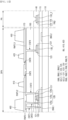
- FIG. 3 is a cross-sectional view taken along line I-I' of FIG. 2 .
- the display device 10 of FIG. 1 may include a first substrate 110, a buffer layer 115, a thin film transistor layer TFTL, and a light emitting element layer EML.
- the first substrate 110 may be a base substrate or a base member and may be made of an insulating material such as a polymer resin.
- the first substrate 110 may be a rigid substrate.
- the buffer layer 115 may be disposed on the first substrate 110.
- the buffer layer 115 may made of an inorganic film that can prevent the penetration of air or moisture.
- the thin film transistor layer TFTL may include a thin film transistor, a gate insulating layer, an interlayer insulating layer, and a via layer.
- the thin film transistor layer TFTL may be disposed on the buffer layer 115 and may constitute a pixel circuit of each of the plurality of pixels.
- the light emitting element layer EML may include the light emitting element 300, an anode electrode, a cathode electrode, an outer bank 450, and a first protective layer PAS1.
- the light emitting element 300 may be provided on the thin film transistor.
- the display device 10 may further include a second planarization layer OC2, a first capping layer CAP1, a first bank BK1, a first wavelength conversion unit WLC1, a second wavelength conversion unit WLC2, a light transmission unit LTU, a second capping layer CAP2, a third planarization layer OC3, a second bank BK2, first to third color filters CF1, CF2, and CF3, a second protective layer PAS2, and an encapsulation layer ENC.
- a second planarization layer OC2 a first capping layer CAP1, a first bank BK1, a first wavelength conversion unit WLC1, a second wavelength conversion unit WLC2, a light transmission unit LTU
- a second capping layer CAP2 a third planarization layer OC3, a second bank BK2, first to third color filters CF1, CF2, and CF3, a second protective layer PAS2, and an encapsulation layer ENC.
- the second planarization layer OC2 may be provided on the light emitting element layer EML and may planarize an upper end of the light emitting element layer EML.
- the second planarization layer OC2 may include an organic material.
- the first capping layer CAP1 may be disposed on the second planarization layer OC2.
- the first capping layer CAP1 may seal the lower surfaces of the first and second wavelength conversion units WLC1 and WLC2 and the light transmission unit LTU.
- the first capping layer may include an inorganic material.
- the first bank BK1 may be disposed in a light blocking area BA on the first capping layer CAP1.
- the first bank BK1 may overlap the second bank BK2 in a thickness direction.
- the first bank BK1 may block light transmission.
- the first bank BK1 may include an organic light blocking material and a liquid repellent component.
- the first and second wavelength conversion units WLC1 and WLC2 and the light transmission unit LTU may be separated to correspond to light emitting areas LA.
- the first wavelength conversion unit WLC1 may be disposed in the first light emitting area LA1 on the first capping layer CAP1.
- the first wavelength conversion unit WLC1 may be surrounded by the first bank BK1.
- the first wavelength conversion unit WLC1 may include a first base resin BS1, a first scattering body SCT1, and a first wavelength shifter WLS1.
- the first base resin BS1 may include a material having relatively high light transmittance.
- the first base resin BS1 may be made of a transparent organic material.
- the first base resin BS1 may include at least one of organic materials such as an epoxy-based resin, an acrylic-based resin, a cardo-based resin, and an imide-based resin.
- the first scattering body SCT1 may have a refractive index different from that of the first base resin BS1 and may form an optical interface together with the first base resin BS1.
- the first wavelength shifter WLS1 may convert or shift a peak wavelength of incident light to a first peak wavelength.
- the first wavelength shifter WLS1 may convert blue light provided in the display device into red light having a single peak wavelength in the range of 61 0 nm to 650 nm and may emit the converted red light.
- the first wavelength shifter WLS1 may be a quantum dot, a quantum rod, or a phosphor.
- the quantum dot may be particulate matter that emits a specific color while electrons transition from a conduction band to a valence band.
- the light emitted by the first wavelength shifter WLS1 may have a full width at half maximum (FWHM) of 45 nm or less, 40 nm or less, or 30 nm or less, and may further improve the color purity and the color reproducibility of the color displayed by the display device.
- FWHM full width at half maximum
- a portion of the blue light provided by the light emitting element layer EML may pass through the first wavelength conversion unit WLC1 without being converted into the red light by the first wavelength shifter WLS1.
- the blue light provided by the light emitting element layer EML light incident on the first color filter CF1 without being converted by the first wavelength conversion unit WLC1 may be blocked by the first color filter CF1.
- the red light converted by the first wavelength conversion unit WLC1 among the blue light provided by the display device may pass through the first color filter CF1 and may be emitted to the outside.
- the first light emitting area LA1 may emit the red light.
- the second wavelength conversion unit WLC2 may be disposed in the second light emitting area LA2 on the first capping layer CAP1.
- the second wavelength conversion unit WLC2 may be surrounded by the first bank BK1.
- the second wavelength conversion unit WLC2 may include a second base resin BS2, a second scattering body SCT2, and a second wavelength shifter WLS2.
- the second base resin BS2 may include a material having relatively high light transmittance.
- the second base resin BS2 may be made of a transparent organic material.
- the second scattering body SCT2 may have a refractive index different from that of the second base resin BS2 and may form an optical interface together with the second base resin BS2.
- the second scattering body SCT2 may include a light scattering material or light scattering particles that scatter at least a portion of transmitted light.
- the second wavelength shifter WLS2 may convert or shift the peak wavelength of the incident light to a second peak wavelength different from the first peak wavelength of the first wavelength shifter WLS1.
- the second wavelength shifter WLS2 may convert the blue light provided in the display device into green light having a single peak wavelength in the range of 510 nm to 550 nm and may emit the converted green light.
- the second wavelength shifter WLS2 may be a quantum dot, a quantum rod, or a phosphor.
- the second wavelength shifter WLS2 may include a material having the same purpose as the material illustrated in the first wavelength shifter WLS1.
- the light transmission unit LTU may be disposed in the third light emitting area LA3 on the first capping layer CAP1.
- the light transmission unit LTU may be surrounded by the first bank BK1.
- the light transmitting unit LTU may transmit the incident light while maintaining a peak wavelength.
- the light transmission unit LTU may include a third base resin BS3 and a third scattering body SCT3.
- the third base resin BS3 may include a material having relatively high light transmittance.
- the third base resin BS3 may be made of a transparent organic material.
- the third scattering body SCT3 may have a refractive index different from that of the third base resin BS3 and may form an optical interface together with the third base resin BS3.
- the third scattering body SCT3 may include a light scattering material or light scattering particles that scatter at least a portion of the transmitted light.
- the first and second wavelength conversion units WLC1 and WLC2 and the light transmission unit LTU are arranged on the light emitting element layer EML through the second planarization layer OC2 and the first capping layer CAP1, and thus the display device does not require a separate substrate for the first and second wavelength conversion units WLC1 and WLC2 and the light transmission unit LTU.
- the second capping layer CAP2 may cover the first and second wavelength conversion units WLC1 and WLC2, the light transmission unit LTU, and the first bank BK1.
- the third planarization layer OC3 may be disposed on the second capping layer CAP2 and may planarize upper ends of the first and second wavelength conversion units WLC1 and WLC2 and the light transmission unit LTU.
- the third planarization layer OC3 may include an organic material.
- the second bank BK2 may be disposed in a light blocking area BA on the third planarization layer OC3.
- the second bank BK2 may overlap the first bank BK1 in the thickness direction.
- the second bank BK2 may block light transmission.
- the first color filter CF1 may be disposed in the first light emitting area LA1 on the third planarization layer OC3.
- the first color filter CF1 may be surrounded by the second bank BK2.
- the first color filter CF1 may overlap the first wavelength conversion unit WLC1 in the thickness direction.
- the first color filter CF1 may selectively transmit light having a first color (for example, red light) and may block or absorb light having a second color (for example, green light) and light having a third color (for example, blue light).
- the second color filter CF2 may be disposed in the second light emitting area LA2 on the third planarization layer OC3.
- the second color filter CF2 may be surrounded by the second bank BK2.
- the second color filter CF2 may overlap the second wavelength conversion unit WLC2 in the thickness direction.
- the second color filter CF2 may selectively transmit the light having the second color (for example, green light) and may block or absorb the light having the first color (for example, red light) and the light having the third color (for example, blue light).
- the third color filter CF3 may be disposed in the third light emitting area LA3 on the third planarization layer OC3.
- the third color filter CF3 may be surrounded by the second bank BK2.
- the third color filter CF3 may overlap the light transmission unit LTU in the thickness direction.
- the third color filter CF3 may selectively transmit the light having the third color (for example, blue light) and may block or absorb the light having the first color (for example, red light) and the light having the second color (for example, green light).
- the first to third color filters CF1, CF2, and CF3 may absorb a portion of light incident from the outside of the display device, thereby reducing reflected light caused by external light.
- the first to third color filters CF1, CF2, and CF3 may prevent color distortion due to the reflection of external light.
- the second protective layer PAS2 may cover the first to third color filters CF1, CF2, and CF3.
- the second protective layer PAS2 may protect the first to third color filters CF1, CF2, and CF3.
- the encapsulation layer ENC may be disposed on the second protective layer PAS2.
- the encapsulation layer ENC may include at least one inorganic film and prevent the penetration of oxygen or moisture.
- the encapsulation layer ENC may include at least one organic film and protect the display device from foreign matter such as dust.
- FIG. 4 is a schematic plan view illustrating one pixel of the display device according to the embodiment.
- each of the sub-pixels PX1 to PX3 may further include a first contact electrode PXL1, a second contact electrode PXL2, a second electrode RMTL2, and a third electrode RMTL3.
- the first contact electrode PXL1 may overlap and be in contact with one end (the other side in a first direction DR1) of the light emitting element 300
- the second contact electrode PXL2 may overlap and be in contact with the other end (one side in the first direction DR1) of the light emitting element 300.
- the plurality of electrodes RMTL2 and RMTL3 may be electrically connected to the light emitting elements 300 and may receive a predetermined voltage so that the light emitting element 300 emits light.
- the plurality of electrodes RMTL2 and RMTL3 may be electrically connected to the light emitting element 300 through the contact electrodes PXL1 and PXL2 and may transmit electrical signals applied to the electrodes RMTL2 and RMTL3 to the light emitting element 300 through the contact electrodes PXL1 and PXL2.
- the second electrode RMTL2 may be a pixel electrode separated for each sub-pixel, and the third electrode RMTL3 may be a common electrode commonly connected along each sub-pixel.
- One of the second electrode RMTL2 and the third electrode RMTL3 may be an anode electrode of the light emitting element 300 and the other one thereof may be a cathode electrode of the light emitting element 300.
- the present disclosure is not limited thereto, and the opposite could be the case.
- FIG. 5 is an equivalent circuit diagram of one sub-pixel of the display device according to the embodiment.
- each sub-pixel of the display device includes three transistors DTR, STR1, and STR2 and one storage capacitor CST in addition to the light emitting element 300.
- the light emitting element 300 emits light according to a current supplied through the drive transistor DTR.
- the light emitting element 300 may be implemented as an OLED, a micro LED, a nano LED, or the like.
- the anode electrode of the light emitting element 300 may be connected to a source electrode 126b (see FIG. 6 ) of the drive transistor DTR, and the cathode electrode may be connected to a second power line ELVSL (alternatively, see 123 and 123' in FIG. 6 ) to which a low potential voltage (second power voltage) lower than a high potential voltage (first power voltage) of a first power line ELVDL (alternatively, see RMTL1 in FIG. 6 ) is supplied.
- the drive transistor DTR adjusts a current flowing from the first power line ELVDL to which the first power voltage is supplied to the light emitting element 300 according to a voltage difference between a gate electrode and the source electrode.
- the gate electrode of the drive transistor DTR may be connected to a first source/drain electrode of the first switching transistor STR1, the source electrode thereof may be connected to a first electrode of the light emitting element 300, and a drain electrode thereof may be connected to the first power line ELVDL to which the first power voltage is applied.
- the first switching transistor STR1 is turned on by a scan signal of a scan line SCL to connect a data line DTL to the gate electrode of the drive transistor DTR.
- a gate electrode of the first switching transistor STR1 may be connected to the scan line SCL, the first source/drain electrode thereof may be connected to the gate electrode of the drive transistor DTR1, and a second source/drain electrode thereof may be connected to the data line DTL.
- the second switching transistor STR2 is turned on by a sensing signal of a sensing signal line SSL to connect a reference voltage line RVL to the source electrode of the drive transistor DTR.
- a gate electrode of the second switching transistor STR2 may be connected to the sensing signal line SSL, a first source/drain electrode thereof may be connected to the reference voltage line RVL, and a second source/drain electrode thereof may be connected to the source electrode of the drive transistor DTR.
- the first source/drain electrode of each of the first and second switching transistors STR1 and STR2 may be a source electrode and the second source/drain electrode thereof may be a drain electrode.
- the present disclosure is not limited thereto, and the opposite could be the case.
- the capacitor CST is formed between the gate electrode and the source electrode of the drive transistor DTR.
- the storage capacitor CST stores a differential voltage between a gate voltage and a source voltage of the drive transistor DTR.
- the drive transistor DTR and the first and second switching transistors STR1 and STR2 may be formed as thin film transistors. Further, in FIG. 3 , the description is made based on the fact that the drive transistor DTR and the first and second switching transistors STR1 and STR2 are formed as an N-type metal oxide semiconductor field effect transistor (MOSFET), but the present disclosure is not limited thereto. That is, the drive transistor DTR and the first and second switching transistors STR1 and STR2 may be formed as a P-type MOSFET, or one thereof may be formed as the N-type MOSFET and the other may be formed as the P-type MOSFET.
- MOSFET metal oxide semiconductor field effect transistor
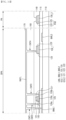
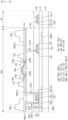
- FIG. 6 is a cross-sectional view taken along line II-II' of FIG. 4 and line III-III' of FIG. 1 .
- FIG. 6 illustrates only a cross section of the first sub-pixel PX1 of FIG. 4 , but the same may be applied to other pixels or sub-pixels.
- FIG. 6 illustrates a cross section across one end and the other end of the light emitting element 300 disposed in the first sub-pixel PX1 of FIG. 4 . Further, FIG. 6 illustrates a cross section of the drive transistor DTR of FIG. 5 .
- the display device 10 may further include a lower metal layer UML disposed between the first substrate 110 and the buffer layer 115, an active material layer 126, a gate insulating layer 130, a first gate conductive layer GCL1, a second gate conductive layer GCL2, an interlayer insulating layer 140, and a via layer 160 of the thin film transistor layer TFTL, and an electrode layer RML, a protective layer 170, a contact electrode layer PXL, an organic layer OGL, an inner bank layer IBL, and an outer bank 450 of the light emitting element layer EML.
- a lower metal layer UML disposed between the first substrate 110 and the buffer layer 115, an active material layer 126, a gate insulating layer 130, a first gate conductive layer GCL1, a second gate conductive layer GCL2, an interlayer insulating layer 140, and a via layer 160 of the thin film transistor layer TFTL, and an electrode layer RML, a protective layer 170, a contact electrode layer PXL, an organic layer OGL,
- the first substrate 110 may be an insulating substrate.
- the first substrate 110 may be made of an insulating material such as glass, quartz, and a polymer resin. Further, the first substrate 110 may be a rigid substrate but may be a flexible substrate capable of bending, folding, rolling, or the like.
- the lower metal layer UML may be disposed on the first substrate 110.
- the lower metal layer UML may include a first lower metal pattern BML1 and a second lower metal pattern BML2.
- the first lower metal pattern BML1 may be disposed to overlap the active material layer 126 of the drive transistor DTR in the thickness direction.
- the second lower metal pattern BML2 may be disposed to overlap the third electrode RMTL3 in the thickness direction.
- the first lower metal pattern BML1 and the second lower metal pattern BML2 are located to be coplanar.
- the lower metal layer UML may include, for example, a light blocking material.
- the first lower metal pattern BML1 may prevent light from entering the active material layer 126.
- the lower metal layer UML may be made of an opaque metal material that blocks light transmission.
- the lower metal layer UML is not limited to the light blocking function.
- the first lower metal pattern BML1 may be electrically connected to the first electrode RMTL1 which will be described below.
- the buffer layer 115 may include the lower metal layer UML and may be entirely disposed on the first substrate 110.
- the buffer layer 115 may be formed on the first substrate 110 to protect the active material layer 126 from moisture penetrating through the first substrate 110 which is vulnerable to moisture permeation, and may be formed through a chemical vapor deposition (CVD) method.
- the buffer layer 115 may be formed as a plurality of alternately stacked inorganic layers.
- the buffer layer 115 may be formed as a multilayer in which one or more inorganic layers of a silicon oxide layer (SiOx), a silicon nitride layer (SiNx), and a silicon oxynitride layer (SiON) are alternately laminated.
- the active material layer 126 may be disposed to partially overlap a gate electrode 121 of the first gate conductive layer GCL1.
- the active material layer 126 may include polycrystalline silicon, single crystalline silicon, an oxide semiconductor, or the like.
- the polycrystalline silicon may be formed by crystallizing amorphous silicon. Examples of the crystallization method include a rapid thermal annealing (RTA) method, a solid phase crystallization (SPC) method, an excimer laser annealing (ELA) method, a metal induced crystallization (MILC) method, a sequential lateral solidification (SLS) method, and the like, but the present disclosure is not limited thereto.
- RTA rapid thermal annealing
- SPC solid phase crystallization
- ESA excimer laser annealing
- MILC metal induced crystallization
- SLS sequential lateral solidification
- the active material layer 126 when the active material layer 126 includes polycrystalline silicon, the active material layer 126 may include a first doped area 126a, a second doped area 126b, and a channel area 126c.
- the channel area 126c may be disposed between the first doped area 126a and the second doped area 126b.
- the first doped area 126a and the second doped area 126b may be areas in which some areas of the active material layer 126 are doped with impurities.
- the active material layer 126 is not necessarily limited to the above.
- the active material layer 126 may include an oxide semiconductor.
- the first doped area 126a may be a first conductive area
- the second doped area 126b may be a second conductive area.
- the oxide semiconductor may be an oxide semiconductor containing indium (In).
- the oxide semiconductor may be indium-tin oxide (ITO), indium-zinc oxide (IZO), indium-gallium oxide (IGO), indium-zinc-tin oxide (IZTO), indium-gallium-tin oxide (IGTO), indium-gallium-zinc-tin oxide (IGZTO), indium-gallium-zinc oxide (IGZO), or the like, but the present disclosure is not limited thereto.
- the gate insulating layer 130 may be disposed on the buffer layer 115 and the active material layer 126.
- the gate insulating layer 130 functions as a gate electrode insulating layer of the drive transistor DTR.
- the gate insulating layer 130 may be formed as a multilayer in which one or more inorganic layers of silicon oxide (SiOx), silicon nitride (SiNx), and silicon oxynitride (SiON) are alternately laminated.
- the gate insulating layer 130 may include a plurality of patterns.
- the gate insulating layer 130 may include a first gate insulating pattern 130 overlapping the gate electrode 121 and the channel area 126c of the active material layer 126, a second gate insulating pattern 130_1 overlapping a signal application electrode 123, and a third gate insulating pattern 130_2 located in the pad area PA and overlapping a first pad part 125.
- the side surfaces of the gate electrode 121 and the first gate insulating pattern 130 overlapping the gate electrode 121 may be aligned, the side surfaces of the signal application electrode 123 and the second gate insulating pattern 130_1 overlapping the signal application electrode 123 may be aligned, and the side surfaces of the first pad part 125 and the third gate insulating pattern 130_2 overlapping the first pad part 125 may be aligned.
- the present disclosure is not limited thereto, and the gate insulating layer 130 may be completely formed without including patterns.
- the first gate conductive layer GCL1 is disposed on the gate insulating layer 130.
- the first gate conductive layer GCL1 may include the gate electrode 121, the signal application electrode 123, and the first pad part 125 located in the pad area PA.
- the gate electrode 121, the signal application electrode 123, and the first pad part 125 of the pad electrode PAD located in the pad area PA may be formed through the same process and made of the same material.
- the gate electrode 121 is disposed to overlap at least a partial area of the active material layer 126.
- the gate electrode 121 may be disposed to overlap the channel area 126c of the active material layer 126 in the thickness direction.
- the gate electrode 121 may overlap the first gate insulating pattern 130, and the side surfaces of the gate electrode 121 may be aligned with the side surfaces of the first gate insulating pattern 130.
- the signal application electrode 123 may overlap the second gate insulating pattern 130_1, and the side surfaces of the signal application electrode 123 may be aligned with the side surfaces of the second gate insulating pattern 130_1.
- the first pad part 125 may overlap the third gate insulating pattern 130_2, and the side surfaces of the first pad part 125 may be aligned with the side surfaces of the third gate insulating pattern 130_2.
- the electrodes 121 and 123 and the pad part 125 of the first gate conductive layer GCL1 may be formed through the same mask as the gate insulating pattern 130 of a lower gate insulating layer.
- the first gate conductive layer GCL1 may be formed as a single layer or a multi-layer made of any one of molybdenum (Mo), aluminum (Al), chromium (Cr), gold (Au), titanium (Ti), nickel (Ni), neodymium (Nd), copper (Cu), or an alloy thereof.
- Mo molybdenum
- Al aluminum
- Cr chromium
- Au gold
- Ti titanium
- Ni nickel
- Nd neodymium
- Cu copper
- the present disclosure is not limited thereto.
- the second gate conductive layer GCL2 may be disposed on the first gate conductive layer GCL1.
- the second gate conductive layer GCL2 may include a sub gate electrode 121' overlapping the gate electrode 121 in the thickness direction, a sub signal application electrode 123' overlapping the signal application electrode 123 in the thickness direction, and a second pad part 125' overlapping the first pad part 125 in the thickness direction.
- the side surfaces of the sub gate electrode 121' may be aligned with the side surfaces of the gate electrode 121, the side surfaces of the sub signal application electrode 123' may be aligned with the side surfaces of the signal application electrode 123, and the side surfaces of the second pad part 125' may be aligned with the side surfaces of the first pad part 125.
- the electrodes 121' and 123' and the pad part 125' of the second gate conductive layer GCL2 may be formed through the same mask as the first gate conductive layer GCL1.
- the first pad part 125 of the pad area PA may be vulnerable to corrosion due to outside air or moisture.
- a contact electrode layer PXL which is in contact with a light emitting element and to which a transparent conductive material is applied, is formed, a capping conductive layer is also formed on the first pad part 125, and thus corrosion of the first pad part 125 is suppressed.
- the cross-sectional structure of the display device in which the first pad part 125 is disposed in the first gate conductive layer GCL1 is applied as in the embodiment, as illustrated in FIG. 6 , a high level difference occurs in the interlayer insulating layer 140.
- the contact electrode layer PXL When the contact electrode layer PXL is formed and when the capping conductive layer is formed on the upper surface and the exposed side surfaces of the interlayer insulating layer 140 and the upper surface of the first pad part 125, it may not be easy to form the capping conductive layer on the exposed side surfaces of the interlayer insulating layer 140 due to the high level difference of the interlayer insulating layer 140.
- the second pad part 125' is immediately formed on the first pad part 125, and thus corrosion of the first pad part 125 is suppressed while making the formation of the capping conductive layer easier.
- the second gate conductive layer GCL2 may include a transparent conductive material.
- the second gate conductive layer GCL2 may include a material such as indium tin oxide (ITO), indium zinc oxide (IZO), and indium tin-zinc oxide (ITZO), but the present disclosure is not limited thereto. Corrosion of the electrodes 121' and 123' and the pad part 125' of the second gate conductive layer GCL2 may be prevented by capping the electrodes 121 and 123 and the pad part 125 of the first gate conductive layer GCL1 thereunder.
- ITO indium tin oxide
- IZO indium zinc oxide
- ITZO indium tin-zinc oxide
- the interlayer insulating layer 140 is disposed on the second gate conductive layer GCL2.
- the interlayer insulating layer 140 may function as an insulating film between the second gate conductive layer GCL2 and other layers arranged above the second gate conductive layer GCL2.
- the interlayer insulating layer 140 may be formed of an inorganic material, for example, silicon oxide (SiOx), silicon nitride (SiNx), or a stacked structure thereof.
- the interlayer insulating layer 140 may partially expose the upper surface of the second pad part 125' in the pad area PA. Although not illustrated, an electrode of the FPCB may be attached to the exposed upper surface of the second pad part 125'.
- the via layer 160 may be disposed on the interlayer insulating layer 140.
- the via layer 160 may include an organic insulating material and perform a surface planarization function.
- the via layer 160 may not be disposed in the pad area PA.
- the electrode layer RML may be disposed on the via layer 160.
- the electrode layer RML may include a first electrode RMTL1, a second electrode RMTL2, and a third electrode RMTL3.
- the first electrode RMTL1 may be electrically connected to the first doped area 126a of the active material layer 126 and the first lower metal pattern BML1.
- the first electrode RMTL1 may be electrically connected to the first lower metal pattern BML1 through a first contact hole CNT1 passing through the via layer 160, the interlayer insulating layer 140, and the buffer layer 115 and may be electrically connected to the first doped area 126a of the active material layer 126 through a second contact hole CNT2 passing through the via layer 160 and the interlayer insulating layer 140.
- the second electrode RMTL2 may be electrically connected to the second doped area 126b of the active material layer 126.
- the second electrode RMTL2 may be electrically connected to the second doped area 126b of the active material layer 126 through a third contact hole CNT3 passing through the via layer 160 and the interlayer insulating layer 140.
- the third electrode RMTL3 may be electrically connected to the sub signal application electrode 123' through a fourth contact hole CNT4 passing through the via layer 160 and the interlayer insulating layer 140.
- Each of the second electrode RMTL2 and the third electrode RMTL3 may be used to form an electric field inside the sub pixel to align the light emitting elements 300. Furthermore, each of the second electrode RMTL2 and the third electrode RMTL3 may be electrically connected to the light emitting element 300.
- the first power voltage may be applied through the first lower metal pattern BML1, and the first power voltage applied through the first lower metal pattern BML1 may be applied to the second electrode RMTL2 through the first electrode RMTL1 and the active material layer 126.
- the second power voltage may be applied through the signal application electrode 123, and the second power voltage applied through the signal application electrode 123 may be applied to the third electrode RMTL3 through the sub signal application electrode 123'.
- the first power voltage applied to the second electrode RMTL2 and the second power voltage applied to the third electrode RMTL3 may be used to align the light emitting elements 300 as described above.
- the light emitting elements 300 may be sprayed onto the second electrode RMTL2 and the third electrode RMTL3 in a state of being dispersed in a predetermined ink through an inkjet process and may be aligned between the second electrode RMTL2 and the third electrode RMTL3 through a method of applying a dieletrophoretic force to the light emitting element 300 by applying an alignment signal between the second electrode RMTL2 and the third electrode RMTL3.
- first power voltage applied to the second electrode RMTL2 may be connected to one end of the light emitting element 300 through the first contact electrode PXL1 and the second power voltage applied to the third electrode RMTL3 may be connected to the other end of the light emitting element 300 through the second contact electrode PXL2 so as to drive the light emitting element 300.
- the second electrode RMTL2 may be an anode electrode
- the third electrode RMTL3 may be a cathode electrode.
- the protective layer 170 may be disposed on the electrode layer RML.
- the protective layer 170 may be formed of an inorganic material, for example, silicon oxide (SiOx), silicon nitride (SiNx), or a stacked structure thereof.
- the protective layer 170 serves to protect the electrode layer RML thereunder from outside air or moisture.
- the contact electrode layer PXL may be disposed on the protective layer 170.
- the contact electrode layer PXL may include the first contact electrode PXL1 connected to the second electrode RMTL2 through a fifth contact hole CNT5 passing through the protective layer 170 and a second contact electrode PXL2 connected to the third electrode RMTL3 through a sixth contact hole CNT6 passing through the protective layer 170.
- the first power voltage is applied to the first contact electrode PXL1 through the second electrode RMTL2
- the second power voltage is applied to the second contact electrode PXL2 through the third electrode RMTL3.
- the first contact electrode PXL1 may cover and be in direct contact with a side surface of one end and a portion of the upper surface of the light emitting element 300
- the second contact electrode PXL2 may cover and be in direct contact with a side surface of the other end and a portion of the upper surface of the light emitting element 300.
- the first and second contact electrodes PXL1 and PXL2 may serve to suppress the movement of the light emitting element 300 by being in contact with the side surface and the portion of the upper surface of the light emitting element 300.
- the first contact electrode PXL1 and the second contact electrode PXL2 may be arranged to be physically spaced apart from each other.
- the contact electrodes PXL1 and PXL2 may include a transparent conductive material.
- the contact electrodes PXL1 and PXL2 may include a material such as indium tin oxide (ITO), indium zinc oxide (IZO), and indium tin zinc oxide (ITZO), but the organic layer OGL may be disposed on the contact electrode layer PXL.
- the organic layer OGL may include a first organic pattern 460 overlapping the first contact electrode PXL1 and a second organic pattern 470 overlapping the second contact electrode PXL2.
- the first organic pattern 460 and the second organic pattern 470 may be arranged to be physically spaced apart from each other.
- the separation space between the first and second organic patterns 460 and 470 may overlap the separation space between the first and second contact electrodes PXL1 and PXL2 in the thickness direction.
- the inner surface of the first organic pattern 460 may be aligned with the inner surface of the first contact electrode PXL1, and the inner surface of the second organic pattern 470 may be aligned with the inner surface of the second contact electrode PXL2.
- the outer surface of the first organic pattern 460 may be aligned with the outer surface of the first contact electrode PXL1
- the present disclosure is not limited thereto.
- the outer surface of the second organic pattern 470 may be aligned with the outer surface of the second contact electrode PXL2
- present disclosure is not limited thereto.
- the inner bank layer IBL and the outer bank 450 may be arranged on the protective layer 170.
- the inner bank layer IBL is directly disposed on the protective layer 170.
- the inner bank layer IBL may include a first inner bank 410 located on one side of the light emitting element 300 and a second inner bank 420 located on the other side of the light emitting element 300.
- the first inner bank 410 and the second inner bank 420 may be arranged to be spaced apart from each other and to face each other. By arranging the inner banks 410 and 420 to be spaced apart from each other and to face each other, an area in which the light emitting element 300 is disposed may be formed therebetween.
- first inner bank 410 and the second inner bank 420 may have a structure in which at least a portion thereof protrudes from the upper surface of the protective layer 170.
- the protruding parts of the first inner bank 410 and the second inner bank 420 may have inclined side surfaces.
- the inner banks 410 and 420 may provide the area in which the light emitting element 300 is disposed.
- the inner banks 410 and 420 may include an organic insulating material such as polyimide (PI), but the present disclosure is not limited thereto.
- the outer bank 450 may be located to be coplanar with the inner bank layer IBL.
- the outer bank 450 may be located outside the first inner bank 410 and outside the second inner bank 420.
- the outer bank 450 may be formed through the same process as the inner bank layer IBL.
- the outer bank 450 and the inner bank layer IBL may be formed through the same mask process, and a height h2 of the outer bank 450 is larger than a height h1 of the inner banks 410 and 420.
- the outer bank 450 and the inner banks 410 and 420 having different heights may be formed using a half tone mask.
- the light emitting element 300 may be an LED, and specifically, the light emitting element 300 may be an inorganic LED having a micrometer or nanometer unit size and made of an inorganic material. Inorganic LEDs may be arranged between two electrodes facing each other that form a polarity when an electric field is formed in a specific direction between the two electrodes. The light emitting elements 300 may be arranged between the electrodes by the electric field formed on the two electrodes.
- the light emitting element 300 may have a shape extending in one direction.
- the light emitting element 300 may have a shape such as a rod, a wire, and a tube.
- the light emitting element 300 may have a cylindrical shape or a rod shape.
- the shape of the light emitting element 300 is not limited thereto, and the light emitting element 300 may have one of various shapes including a shape of a polygonal column such as a regular hexahedron, a rectangular parallelepiped, and a hexagonal column or a shape that extends in one direction but has a partially inclined outer surface.
- a plurality of semiconductors included in the light emitting element 300 which will be described below, may have a structure in which the semiconductors are sequentially arranged or stacked in one direction.
- the light emitting element 300 may include a semiconductor layer doped with a predetermined conductive type (for example, a p type or an n type) impurity.
- the semiconductor layer may receive an electrical signal applied from an external power source and emit the electrical signal as light in a specific wavelength band.
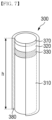
- FIG. 7 is a schematic view of the light emitting element according to the embodiment.
- the light emitting element 300 may include a first semiconductor layer 310, a second semiconductor layer 320, an active layer 330, an electrode layer 370, and an insulating film 380.
- the first semiconductor layer 310 may be an n-type semiconductor.
- the first semiconductor layer 310 may include a semiconductor material having a chemical formula of AlxGayln1-x-yN (0 ⁇ x ⁇ 1, 0 ⁇ y ⁇ 1, and 0 ⁇ x+y ⁇ 1).
- the semiconductor material may be one or more of n-type doped AlGaInN, GaN, AlGaN, InGaN, AIN, and InN.
- the first semiconductor layer 310 may be doped with an n-type dopant, and for example, the n-type dopant may be Si, Ge, Sn, or the like.
- the first semiconductor layer 310 may be n-GaN doped with n-type Si. Although a length of the first semiconductor layer 310 may be in the range of 1.5 ⁇ m to 5 ⁇ m, the present disclosure is not limited thereto.
- the second semiconductor layer 320 is disposed on the active layer 330 which will be described below.
- the second semiconductor layer 320 may be a p-type semiconductor, and as an example, when the light emitting element 300 emits light in the wavelength band of blue or green, the second semiconductor layer 320 may include a semiconductor material having a chemical formula of AlxGayln1-x-yN (0 ⁇ x ⁇ 1, 0 ⁇ y ⁇ 1, and 0 ⁇ x+y ⁇ 1).
- the semiconductor material may be one or more of p-type doped AlGaInN, GaN, AlGaN, InGaN, AIN, and InN.
- the second semiconductor layer 320 may be doped with a p-type dopant, and for example, the p-type dopant may be Mg, Zn, Ca, Se, Ba, or the like. In the exemplary embodiment, the second semiconductor layer 320 may be p-GaN doped with p-type Mg. Although the length of the second semiconductor layer 320 may be in the range of 0.05 ⁇ m to 0.10 ⁇ m, the present disclosure is not limited thereto.
- the first semiconductor layer 310 and the second semiconductor layer 320 are configured as one layer, the present disclosure is not limited thereto.
- the first semiconductor layer 310 and the second semiconductor layer 320 may further include a larger number of layers, for example, a clad layer or a tensile strain barrier reducing (TSBR) layer.
- TSBR tensile strain barrier reducing
- the active layer 330 is disposed between the first semiconductor layer 310 and the second semiconductor layer 320.
- the active layer 330 may include a material having a single or multiple quantum well structure.
- the active layer 330 may have a structure in which a plurality of quantum layers and a plurality of well layers are alternately laminated.
- the active layer 330 may emit light by combination of an electron-hole pair according to an electrical signal applied through the first semiconductor layer 310 and the second semiconductor layer 320.
- the active layer 330 may include a material such as AlGaN and AlGaInN.
- the quantum layer may include AlGaN or AlGaInN
- the well layer may include GaN or AlInN
- the active layer 330 may include AlGaInN as the quantum layer and AlInN as the well layer, and as described above, the active layer 330 may emit blue light whose central wavelength band is in the range of 450 nm to 495 nm.
- the active layer 330 may have a structure in which semiconductor materials having large band gap energy and semiconductor materials having small band gap energy are alternately laminated, and may include other group 3 to group 5 semiconductor materials according to the wavelength band of the emitted light.
- the light emitted by the active layer 330 is not limited to the light in the blue wavelength band, and in some cases, the active layer 330 may emit light in the wavelength band of red or green.
- the length of the active layer 330 may be in the range of 0.05 ⁇ m to 0.10 ⁇ m, the present disclosure is not limited thereto.
- the light emitted by the active layer 330 may be emitted not only to the outer surface of the light emitting element 300 in the lengthwise direction, but also to both side surfaces.
- the directionality of the light emitted by the active layer 330 is not limited to one direction.
- the electrode layer 370 may be an ohmic contact electrode. However, the present disclosure is not limited thereto, and the electrode layer 370 may be a Schottky contact electrode.
- the light emitting element 300 may include at least one electrode layer 370. Although it is illustrated in FIG. 7 that the light emitting element 300 includes one electrode layer 370, the present disclosure is not limited thereto. In some cases, the light emitting element 300 may include a larger number of electrode layers 370 or the electrode layers 370 may be omitted. The following description of the light emitting element 300 may be equally applied even when the number of electrode layers 370 is changed or other structures are further included.
- the electrode layer 370 may reduce resistance between the light emitting element 300 and the electrode or contact electrode.
- the electrode layer 370 may include a conductive metal.
- the electrode layer 370 may include at least one of aluminum (Al), titanium (Ti), indium (In), gold (Au), silver (Ag), indium tin oxide (ITO), indium zinc oxide (IZO), and indium tin zinc oxide (ITZO).
- the electrode layer 370 may include a semiconductor material doped with an n-type or p-type impurity.
- the electrode layer 370 may include the same material or different materials, and the present disclosure is not limited thereto.
- the insulating film 380 is disposed to surround the outer surfaces of the plurality of semiconductor layers and the electrode layers described above.
- the insulating film 380 may be disposed to surround at least the outer surface of the active layer 330 or may extend in one direction in which the light emitting element 300 extends.
- the insulating film 380 may function to protect the above members.
- the insulating film 380 may be formed to surround the side surfaces of the members and may be formed so that both ends of the light emitting element 300 in a lengthwise direction are exposed.
- the insulating film 380 is formed to extend in the lengthwise direction of the light emitting element 300 and to cover the first semiconductor layer 310 to the electrode layer 370, the present disclosure is not limited thereto.
- the insulating film 380 may cover only a partial outer surface of the semiconductor layers in addition to the active layer 330 or cover only a partial outer surface of the electrode layer 370, and thus the outer surface of the electrode layer 370 may be partially exposed. Further, the insulating film 380 may be formed such that the upper surface in a cross section in a region adjacent to at least one end of the light emitting element 300 is round.
- the thickness of the insulating film 380 may be in the range of 10 nm to 1.0 ⁇ m, the present disclosure is not limited thereto. Preferably, the thickness of the insulating film 380 may be about 40 nm.
- the insulating film 380 may include materials having insulating properties, for example, silicon oxide (SiOx), silicon nitride (SiNx), silicon oxynitride (SiOxNy), aluminum nitride (AIN), aluminum oxide (Al2O3), or the like. Accordingly, an electrical short circuit that may occur when the active layer 330 is in direct contact with an electrode through which an electrical signal is transmitted to the light emitting element 300 can be prevented. Further, since the insulating film 380 protects the outer surface of the light emitting element 300 in addition to the active layer 330, a decrease in luminous efficiency can be prevented.
- the outer surface of the insulating film 380 may be surface-treated.
- the light emitting elements 300 may be sprayed and arranged onto the electrode in a state of being dispersed in a predetermined ink.
- the surface of the insulating film 380 may be subjected to hydrophobic or hydrophilic treatment.
- the light emitting element 300 may have a length h of 1 ⁇ m to 10 ⁇ m or 2 ⁇ m to 6 ⁇ m, and preferably 3 ⁇ m to 5 ⁇ m. Further, a diameter of the light emitting element 300 may be in the range of 300 nm to 700 nm, and an aspect ratio of the light emitting element 300 may be in the range of 1.2 to 100. However, the present disclosure is not limited thereto.
- the plurality of light emitting elements 300 included in the display device 10 may have different diameters according to a composition difference of the active layer 330. Preferably, the diameter of the light emitting element 300 may be about 500 nm.
- the inner bank layer IBL and the outer bank 450 are formed to be coplanar through the same process, and thus the number of masks can be reduced.
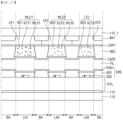
- FIGS. 8 to 14 are cross-sectional views of process operations of a method of manufacturing a display device according to the embodiment.
- the via layer 160 is formed on the interlayer insulating layer 140.
- the formation of the via layer 160 includes forming a via material layer on the interlayer insulating layer 140 and forming a first through-hole CNT1' to a fourth through-hole CNT4'.
- Each of the through-hole CNT1' to CNT4' extends from the upper surface of the via layer 160 to the lower surface of the via layer 160 (the upper surface of the interlayer insulating layer 140).
- the first to fourth contact holes CNT1 to CNT4 are formed.
- the first contact hole CNT1 is formed by further passing through the interlayer insulating layer 140 and the buffer layer 115 from the first through-hole CNT1'
- the second contact hole CNT2 is formed by further passing through the interlayer insulating layer 140 from the second through-hole CNT2'
- the third contact hole CNT3 is formed by further passing through the interlayer insulating layer 140 from the third through-hole CNT3'
- the fourth contact hole CNT4 is formed by further passing through the interlayer insulating layer 140 from the fourth through-hole CNT4'.
- the electrode layer RML is formed on the via layer 160.
- the electrode layer RML fills the first to fourth contact holes CNT1 to CNT4, which are electrically connected to the first lower metal pattern BML1, the first doped area 126a, the second doped area 126b, and the sub signal application electrode 123', respectively.
- the first to fourth electrodes RMTL1 to RMTL4 are formed from the electrode layer RML.
- the electrodes RMTL1 to RMTL4 are physically spaced apart from each other.
- the protective layer 170 is formed by forming a protective material layer on the electrodes RMTL1 to RMTL4 and forming the fifth and sixth contact holes CNT5 and CNT6 in the protective material layer.
- the fifth contact hole CNT5 overlaps the second electrode RMTL2 in the thickness direction and the sixth contact hole CNT6 overlaps the third electrode RMTL3 in the thickness direction.
- the inner bank layer IBL including the first inner bank 410 and the second inner bank 420 and the outer bank 450 are formed on the protective layer 170.
- the inner bank layer IBL and the outer bank 450 may be simultaneously formed through the same process.
- the inner bank layer IBL and the outer bank 450 may be formed through a mask process.
- the inner bank layer IBL and the outer bank 450 may be formed through a half tone mask, and thus the inner bank layer IBL and the outer bank 450 may have different heights.
- the outer bank 450 is not exposed, an area between the inner bank layer IBL and the outer bank 450 is fully exposed, and the inner bank layer IBL is half-exposed.
- the light emitting elements 300 are formed between the first and second inner banks 410 and 420 on the protective layer 170.
- the light emitting elements 300 are formed by being arranged through the alignment signal applied from the second electrode RMTL2 and the third electrode RMTL3 described above in FIG. 6 .
- the contact electrode layer PXL is formed on the protective layer 170 and the light emitting element 300.
- the contact electrode layer PXL may fill the fifth and sixth contact holes CNT5 and CNT6 which are electrically connected to the second and third electrodes RMTL and RMTL3, respectively.
- the organic layer OGL is formed on the contact electrode layer PXL.
- the organic layer OGL may include a first organic pattern 460 and a second organic pattern 470.
- the first organic pattern 460 and the second organic pattern 470 may be located to be spaced apart from each other with a predetermined separation space therebetween.
- the first contact electrode PXL1 and the second contact electrode PXL2 are formed using the first and second organic patterns 460 and 470.
- the first contact electrode PXL1 and the second contact electrode PXL2 are spaced apart from each other with a predetermined separation space therebetween, the separation space between the first and second contact electrodes PXL1 and PXL2 overlaps the separation space between the first and second organic patterns 460 and 470 in the thickness direction.
- FIG. 15 is a cross-sectional view illustrating a part of a display device according to another embodiment.
- the display device differs from the display device of FIG. 6 in that the outer bank and the inner bank layer IBL of FIG. 6 are integrally formed.
- the outer bank 450 may not be exposed in the exposure process of the mask process, the inner bank layer IBL may be half-exposed, and an area between the inner bank layer IBL and the outer bank 450 may be half-exposed, which is like the inner bank layer IBL.
- FIG. 16 is a cross-sectional view illustrating a part of the display device according to another embodiment.
- the display device according to the present embodiment differs from the display device of FIG. 6 in that a first contact electrode PXL1_1 and a second contact electrode PXL2_1 are located to not be coplanar.
- the display device may further include a first insulating layer 52, a second insulating layer 53, and a third insulating layer 54.
- the first insulating layer 52 is disposed on the light emitting element 300.
- the first insulating layer 52 may be directly disposed at a central portion of the upper surface of the light emitting element 300.
- the first contact electrode PXL1_1 may be in contact with the side surface and the upper surface on one end side of the light emitting element 300 and may be in contact with the side surface and the upper surface on one end side of the first insulating layer 52.
- the second insulating layer 53 may be disposed on the outer bank 450, the first inner bank 410, and the first contact electrode PXL1_1.
- the side surface on the other end side of the second insulating layer 53 may be aligned with the side surface on the other end side of the first insulating layer 52, the present disclosure is not limited thereto.
- the second contact electrode PXL2_1 may be in contact with the side surface and the upper surface on the other end side of the light emitting element 300 and may be in contact with the side surface and the upper surface on the other end side of the first insulating layer 52.
- the third insulating layer 54 may be disposed on the second insulating layer 53, the second contact electrode PXL2_1, the second inner bank 420, and the outer bank 450.
- FIG. 17 is a cross-sectional view of the display device according to still another embodiment.
- the display device according to the present embodiment differs from the display device of FIG. 3 in that a second substrate 110_1 opposite to the first substrate 110 is further provided.
- the second substrate 110_1 is opposite to the first substrate 110.
- the second substrate 110_1 may include the same material as the materials exemplified in the first substrate 110.
- the first bank BK1 is disposed on one surface of the second substrate 110_1 facing the first substrate 110.
- the first bank BK1 may be disposed in the light blocking area BA.
- the first to third color filters CF1, CF2, and CF3 may be arranged on the first bank BK1 and one surface of the second substrate 110_1 facing the first substrate 110.
- the first color filter CF1 may be disposed in the first light emitting area LA1
- the second color filter CF2 may be disposed in the second light emitting area LA2
- the third color filter CF3 may be disposed in the third light emitting area LA3.
- the first capping layer CAP1 may be disposed on the first to third color filters CF1, CF2, and CF3.
- the second bank BK2 may be disposed on the first capping layer CAP1.
- the second bank BK2 may be disposed in the light blocking area BA.
- the first and second wavelength conversion units WLC1 and WLC2 and the light transmission unit LTU may be arranged between adjacent second banks BK2.
- the second capping layer CAP2 may be disposed on the first and second wavelength conversion units WLC1 and WLC2, the light transmission unit LTU, and the second bank BK2.
- a filling layer FIL may be disposed between the first protective layer PAS1 and the second capping layer CAP2.
- FIG. 18 is a cross-sectional view illustrating a part of a display device according to yet another embodiment.
- the display device according to the present embodiment differs from the display device of FIG. 6 in that the third electrode RMTL3 may be further connected to the second lower metal pattern BML2 through a fourth contact hole CNT4_1.
- the fourth contact hole CNT4_1 may pass through the via layer 160, the interlayer insulating layer 140, and the buffer layer 115 in the thickness direction.
- the second power voltage may be applied from the second lower metal pattern BML2 and may be provided to the third electrode RMTL3.
- the fourth contact hole CNT4 may be omitted and the third electrode RMTL3 may receive the second power voltage only through the fourth contact hole CNT4_1.
- the second power voltage is applied through the second lower metal pattern BML2 and the second lower metal pattern BML2 and the sub signal application electrode 123' are connected using the third electrode RMTL3 as a bridge electrode.
- the second power voltage is applied through the sub signal application electrode 123' and the sub signal application electrode 123' and the second lower metal pattern BML2 are connected using the third electrode RMTL3 as a bridge electrode.
Landscapes
- Physics & Mathematics (AREA)
- General Physics & Mathematics (AREA)
- Optics & Photonics (AREA)
- Electroluminescent Light Sources (AREA)
- Devices For Indicating Variable Information By Combining Individual Elements (AREA)
Abstract
Description
- The present disclosure relates to a display device and a method of manufacturing the same.
- The importance of display devices is increasing with the development of multimedia. In response to this, various types of display devices such as organic light emitting diode (OLED) displays and liquid crystal displays (LCDs) are being used.
- Devices for displaying images of display devices include display panels such as organic light emitting display panels and liquid crystal display panels. Among them, the light emitting display panel may include a light emitting element. For example, light emitting diodes (LEDs) include OLEDs using organic materials as fluorescent materials, inorganic LEDs using inorganic materials as fluorescent materials, and the like.
- The inorganic LEDs using inorganic semiconductors as fluorescent materials advantageously have durability even in a high temperature environment and have high efficiency of blue light as compared to the OLEDs. Further, even in a manufacturing process pointed out as a limitation of the existing inorganic LED elements, a transfer method using a dielectrophoresis (DEP) method has been developed. Accordingly, research on the inorganic LEDs having excellent durability and efficiency as compared to the OLEDs is ongoing.
- Aspects of the disclosure provide a display device formed with a small number of masks.
- Another aspect of the present disclosure provides a method of manufacturing a display device, by which the display device is manufactured using a small number of masks.
- It should be noted that aspects of the present disclosure are not limited to the above-mentioned aspects, and other unmentioned aspects of the present disclosure will be clearly understood by those skilled in the art from the following descriptions.
- According to an embodiment, a display device comprises a first substrate including a display area and a non-display area located around the display area; an active material layer disposed on the first substrate and including a channel area, a first doped area on one side of the channel area, and a second doped area on the other side of the channel area; a gate insulating layer disposed on the active material layer; a first conductive layer disposed on the gate insulating layer and including a gate electrode disposed to overlap the channel area and a signal application electrode; an interlayer insulating layer disposed on the first conductive layer; a via layer disposed on the interlayer insulating layer; a second conductive layer disposed on the via layer and including a first electrode electrically connected to the first doped area through a contact hole passing through the via layer and the interlayer insulating layer, a second electrode electrically connected to the second doped area through a contact hole passing through the via layer and the interlayer insulating layer, and a third electrode electrically connected to the signal application electrode through a contact hole passing through the via layer and the interlayer insulating layer; a first insulating layer disposed on the second conductive layer; a light emitting element disposed on the first insulating layer of the display area; and a third conductive layer disposed on the light emitting element, connected to the light emitting element, and including a first contact electrode electrically connected to the second electrode through a contact hole passing through the first insulating layer and a second contact electrode electrically connected to the third electrode through a contact hole passing through the first insulating layer.
- According to another embodiment, a display device comprises a first substate; a first lower metal pattern and a second lower metal pattern disposed on the first substrate; a buffer layer disposed on the first lower metal pattern and the second lower metal pattern; an active material layer disposed on the first substrate and including a channel area, a first doped area on one side of the channel area, and a second doped area on the other side of the channel area; a gate insulating layer disposed on the active material layer; a first conductive layer disposed on the gate insulating layer and including a gate electrode disposed to overlap the channel area; an interlayer insulating layer disposed on the first conductive layer; a via layer disposed on the interlayer insulating layer; a second conductive layer disposed on the via layer and including a first electrode electrically connected to the first doped area through a contact hole passing through the via layer and the interlayer insulating layer and electrically connected to the first lower metal pattern through a contact hole passing through the via layer, the interlayer insulating layer, and the buffer layer, a second electrode electrically connected to the second doped area through a contact hole passing through the via layer and the interlayer insulating layer, and a third electrode electrically connected to the second lower metal pattern through a contact hole passing through the interlayer insulating layer and the buffer layer; a first insulating layer disposed on the second conductive layer; a light emitting element disposed on the first insulating layer; and a third conductive layer disposed on the light emitting element and including a first contact electrode electrically connected to the second electrode through a contact hole passing through the first insulating layer and a second contact electrode electrically connected to the third electrode through a contact hole passing through the first insulating layer.
- According to still another embodiment, a method of manufacturing a display device, the method comprises forming a lower metal layer on a first substrate and a buffer layer on the lower metal layer; forming an active material layer including a channel area on the buffer layer, a first doped area on one side of the channel area, and a second doped area on the other side of the channel area; forming a first gate insulating layer and a second gate insulating layer on the active material layer; forming a gate electrode on the first gate insulating layer and forming a signal application electrode on the second gate insulating layer; forming an interlayer insulating layer on the gate electrode and the signal application electrode; forming a via layer on the interlayer insulating layer; forming first to fourth contact holes passing through the via layer; extending the first to fourth contact holes to the lower metal layer, the active material layer, and the signal application electrode; forming an electrode layer inside the first to fourth contact holes and on the via layer; forming a first electrode, a second electrode, and a third electrode by patterning the electrode layer; forming a first insulating layer on the first electrode, the second electrode, and the third electrode; forming inner banks and outer banks on the first insulating layer through a half-tone mask; forming a light emitting element on the first insulating layer by applying an alignment signal to the second electrode and the third electrode; forming a contact electrode layer on the light emitting element; forming a first organic pattern and a second organic pattern, which are separated from each other, on the contact electrode layer; and separating the contact electrode layer into a first contact electrode overlapping the first organic pattern and a second contact electrode overlapping the second organic pattern.
- The details of other embodiments are included in the detailed description and the accompanying drawings.
- The display device according to an embodiment is manufactured with a small number of masks, and thus simplification of a process during the manufacturing can be achieved.
- In the method of manufacturing a display device according to an embodiment, a display device is manufactured with a small number of masks, and thus simplification of a process can be achieved.
- The effects according to the embodiments are not limited by the contents exemplified above, and more various effects are included in this disclosure.
-
-
FIG. 1 is a plan view of a display device according to an embodiment; -
FIG. 2 is a plan view illustrating pixels of the display device according to the embodiment; -
FIG. 3 is a cross-sectional view taken along line I-I' ofFIG. 2 ; -
FIG. 4 is a schematic plan view illustrating one pixel of the display device according to the embodiment; -
FIG. 5 is an equivalent circuit diagram of one sub-pixel of the display device according to the embodiment; -
FIG. 6 is a cross-sectional view taken along line II-II' ofFIG. 4 and line III-III' ofFIG. 1 ; -
FIG. 7 is a schematic view of a light emitting element according to the embodiment; -
FIGS. 8 to 14 are cross-sectional views of process operations of a method of manufacturing a display device according to the embodiment; -
FIG. 15 is a cross-sectional view illustrating a part of a display device according to another embodiment; -
FIG. 16 is a cross-sectional view illustrating a part of a display device according to still another embodiment; -
FIG. 17 is a cross-sectional view of the display device according to still another embodiment; and -
FIG. 18 is a cross-sectional view illustrating a part of a display device according to yet another embodiment. - The present disclosure will now be described more fully hereinafter with reference to the accompanying drawings, in which preferred embodiments of the disclosure are shown. This disclosure may, however, be embodied in different forms and should not be construed as limited to the embodiments set forth herein. Rather, these embodiments are provided so that this disclosure will be thorough and complete, and will fully convey the scope of the disclosure to those skilled in the art.
- It will also be understood that when a layer is referred to as being "on" another layer or substrate, it can be directly on the other layer or substrate, or intervening layers may also be present. The same reference numbers indicate the same components throughout the specification.
- It will be understood that, although the terms "first," "second," etc. may be used herein to describe various elements, these elements should not be limited by these terms. These terms are only used to distinguish one element from another element. For instance, a first element discussed below could be termed a second element without departing from the teachings of the present disclosure. Similarly, the second element could also be termed the first element.
- Hereinafter, embodiments will be described with reference to the accompanying drawings.
-
FIG. 1 is a plan view of a display device according to an embodiment. - Referring to
FIG. 1 , adisplay device 10 displays moving images and a still image. Thedisplay device 10 may refer to as any one of electronic devices providing a display screen. For example, a television, a laptop, a monitor, a billboard, an Internet of Things (IoT) device, a mobile phone, a smart phone, a tablet personal computer (PC), an electronic watch, a smart watch, a watch phone, a head mounted display, a mobile communication terminal, an electronic notebook, an electronic book, a portable multimedia player (PMP), a navigation device, a game console, a digital camera, a camcorder, or the like that provide a display screen may be provided as thedisplay device 10. - The
display device 10 includes a display panel providing a display screen. Examples of the display panel include a light emitting diode (LED) display panel, an organic LED (OLED) panel, a quantum dot light emitting display panel, a plasma display panel, a field emission display panel, and the like. Hereinafter, a case in which the LED display panel is applied as an example of the display panel will be described, but the present disclosure is not limited thereto, and when the same technical spirit is applicable, the present disclosure may be applied to other display panels. - The shape of the
display device 10 may be variously modified. For example, thedisplay device 10 may have a shape such as a long horizontal rectangle, a long vertical rectangle, a square, a quadrangle having rounded corners (vertexes), other polygonal shapes, and a circle. The shape of a display area DPA of thedisplay device 10 may also be similar to the overall shape of thedisplay device 10.FIG. 1 illustrates thedisplay device 10 and the display area DPA having a long horizontal rectangle shape. - The
display device 10 may include the display area DPA and a non-display area NDA. The display area DPA is an area where a screen may be displayed and the non-display area NDA is an area where the screen is not displayed. The display area DPA may refer to as an active area and the non-display area NDA may refer to as an inactive area. The display area DPA may generally occupy the center of thedisplay device 10. - The display area DPA may include a plurality of pixels PX. The plurality of pixels PX may be arranged in a matrix form. The shape of each pixel PX may be a rectangle or a square in a plan view, but the present disclosure is not limited thereto, and the shape of each pixel PX may be a rhombus shape in which each side is inclined in one direction. The pixels PX may be alternately arranged in a stripe type or a PenTile type. Further, each of the pixels PX may include one or more light emitting elements configured to emit light in a specific wavelength band and may display a specific color.
- The non-display area NDA may be disposed around the display area DPA. The non-display area NDA may completely or partially surround the display area DPA. The display area DPA may have a rectangular shape, and the non-display area NDA may be disposed adjacent to four sides of the display area DPA. The non-display area NDA may configure a bezel of the
display device 10. - A flexible printed circuit board (FPCB) may be attached to the non-display area NDA. A plurality of FPCBs may be provided, and the plurality of FPCBs may be arranged in a first direction DR1. A driving integrated circuit SIC may be mounted on each FPCB. The driving integrated circuit SIC may be provided in the form of a driving chip.
- Meanwhile, the non-display area NDA may further include a pad area PA in which a pad electrode PAD coupled to the FPCB is disposed. A plurality of pad electrodes PAD may be provided and arranged in the first direction DR1.
-
FIG. 2 is a plan view illustrating pixels of the display device according to the embodiment. - Referring to
FIG. 2 , each of the plurality of pixels PX may include a first sub-pixel PX1, a second sub-pixel PX2, and a third sub-pixel PX3. The first sub-pixel PX1 may emit light having a first color, the second sub-pixel PX2 may emit light having a second color, and the third sub-pixel PX3 may emit light having a third color. The first color may be blue, the second color may be green, and the third color may be red. However, the present disclosure is not limited thereto, and each of the sub-pixels PX1 to PX3 may emit light having the same color. Further,FIG. 2 illustrates that the pixel PX includes three sub-pixels, but the present disclosure is not limited thereto, and the pixel PX may include a larger number of sub-pixels. - Each of the sub-pixels PX1 to PX3 of the
display device 10 may include an area defined as a light emitting area LA. The first sub-pixel PX1 may include a first light emitting area LA1, the second sub-pixel PX2 may include a second light emitting area LA2, and the third sub-pixel PX3 may include a third light emitting area LA3. - The light emitting area LA may be defined as an area in which a light emitting element 300 (see
FIG. 3 ) included in thedisplay device 10 is disposed and through which light in a specific wavelength band is emitted. The light emitting element may include an active layer 330 (seeFIG. 7 ) and theactive layer 330 may emit light in a specific wavelength band without directionality. The light emitted from theactive layer 330 of thelight emitting element 300 may be emitted in a lateral direction of thelight emitting element 300 as well as directions toward both ends of thelight emitting element 300. The light emitting area LA may include an area where thelight emitting element 300 is disposed and may include an area which is adjacent to thelight emitting element 300 and through which the light emitted from thelight emitting element 300 is emitted. - Further, the present disclosure is not limited thereto, and the light emitting area LA may include an area in which the light emitted from the
light emitting element 300 is reflected or refracted by another member and is emitted. A plurality oflight emitting elements 300 may be arranged in each of the sub-pixels PX1 to PX3, and the light emitting area LA including an area where thelight emitting elements 300 are arranged and an area adjacent thereto may be formed. - Although not illustrated in the drawing, each of the sub-pixels PX1 to PX3 of the
display device 10 may include a non-emission area BA defined as an area other than the light emitting area LA. The non-emission area BA may be an area in which thelight emitting elements 300 are not arranged and through which the light is not emitted because the light emitted from thelight emitting elements 300 does not reach the area. -
FIG. 3 is a cross-sectional view taken along line I-I' ofFIG. 2 . - Referring to
FIG. 3 , thedisplay device 10 ofFIG. 1 may include afirst substrate 110, abuffer layer 115, a thin film transistor layer TFTL, and a light emitting element layer EML. - The
first substrate 110 may be a base substrate or a base member and may be made of an insulating material such as a polymer resin. For example, thefirst substrate 110 may be a rigid substrate. - The
buffer layer 115 may be disposed on thefirst substrate 110. Thebuffer layer 115 may made of an inorganic film that can prevent the penetration of air or moisture. - The thin film transistor layer TFTL may include a thin film transistor, a gate insulating layer, an interlayer insulating layer, and a via layer. The thin film transistor layer TFTL may be disposed on the
buffer layer 115 and may constitute a pixel circuit of each of the plurality of pixels. - The light emitting element layer EML may include the
light emitting element 300, an anode electrode, a cathode electrode, anouter bank 450, and a first protective layer PAS1. Thelight emitting element 300 may be provided on the thin film transistor. - The
display device 10 may further include a second planarization layer OC2, a first capping layer CAP1, a first bank BK1, a first wavelength conversion unit WLC1, a second wavelength conversion unit WLC2, a light transmission unit LTU, a second capping layer CAP2, a third planarization layer OC3, a second bank BK2, first to third color filters CF1, CF2, and CF3, a second protective layer PAS2, and an encapsulation layer ENC. - The second planarization layer OC2 may be provided on the light emitting element layer EML and may planarize an upper end of the light emitting element layer EML. The second planarization layer OC2 may include an organic material.
- The first capping layer CAP1 may be disposed on the second planarization layer OC2. The first capping layer CAP1 may seal the lower surfaces of the first and second wavelength conversion units WLC1 and WLC2 and the light transmission unit LTU. The first capping layer may include an inorganic material.
- The first bank BK1 may be disposed in a light blocking area BA on the first capping layer CAP1. The first bank BK1 may overlap the second bank BK2 in a thickness direction. The first bank BK1 may block light transmission.
- The first bank BK1 may include an organic light blocking material and a liquid repellent component.
- Since the first bank BK1 includes a light repellent component, the first and second wavelength conversion units WLC1 and WLC2 and the light transmission unit LTU may be separated to correspond to light emitting areas LA.
- The first wavelength conversion unit WLC1 may be disposed in the first light emitting area LA1 on the first capping layer CAP1. The first wavelength conversion unit WLC1 may be surrounded by the first bank BK1. The first wavelength conversion unit WLC1 may include a first base resin BS1, a first scattering body SCT1, and a first wavelength shifter WLS1.
- The first base resin BS1 may include a material having relatively high light transmittance. The first base resin BS1 may be made of a transparent organic material. For example, the first base resin BS1 may include at least one of organic materials such as an epoxy-based resin, an acrylic-based resin, a cardo-based resin, and an imide-based resin.
- The first scattering body SCT1 may have a refractive index different from that of the first base resin BS1 and may form an optical interface together with the first base resin BS1.
- The first wavelength shifter WLS1 may convert or shift a peak wavelength of incident light to a first peak wavelength. For example, the first wavelength shifter WLS1 may convert blue light provided in the display device into red light having a single peak wavelength in the range of 61 0 nm to 650 nm and may emit the converted red light. The first wavelength shifter WLS1 may be a quantum dot, a quantum rod, or a phosphor. The quantum dot may be particulate matter that emits a specific color while electrons transition from a conduction band to a valence band.
- The light emitted by the first wavelength shifter WLS1 may have a full width at half maximum (FWHM) of 45 nm or less, 40 nm or less, or 30 nm or less, and may further improve the color purity and the color reproducibility of the color displayed by the display device.
- A portion of the blue light provided by the light emitting element layer EML may pass through the first wavelength conversion unit WLC1 without being converted into the red light by the first wavelength shifter WLS1. Among the blue light provided by the light emitting element layer EML, light incident on the first color filter CF1 without being converted by the first wavelength conversion unit WLC1 may be blocked by the first color filter CF1. Further, the red light converted by the first wavelength conversion unit WLC1 among the blue light provided by the display device may pass through the first color filter CF1 and may be emitted to the outside. Thus, the first light emitting area LA1 may emit the red light.
- The second wavelength conversion unit WLC2 may be disposed in the second light emitting area LA2 on the first capping layer CAP1. The second wavelength conversion unit WLC2 may be surrounded by the first bank BK1. The second wavelength conversion unit WLC2 may include a second base resin BS2, a second scattering body SCT2, and a second wavelength shifter WLS2.
- The second base resin BS2 may include a material having relatively high light transmittance. The second base resin BS2 may be made of a transparent organic material.
- The second scattering body SCT2 may have a refractive index different from that of the second base resin BS2 and may form an optical interface together with the second base resin BS2. For example, the second scattering body SCT2 may include a light scattering material or light scattering particles that scatter at least a portion of transmitted light.
- The second wavelength shifter WLS2 may convert or shift the peak wavelength of the incident light to a second peak wavelength different from the first peak wavelength of the first wavelength shifter WLS1. For example, the second wavelength shifter WLS2 may convert the blue light provided in the display device into green light having a single peak wavelength in the range of 510 nm to 550 nm and may emit the converted green light. The second wavelength shifter WLS2 may be a quantum dot, a quantum rod, or a phosphor. The second wavelength shifter WLS2 may include a material having the same purpose as the material illustrated in the first wavelength shifter WLS1.
- The light transmission unit LTU may be disposed in the third light emitting area LA3 on the first capping layer CAP1. The light transmission unit LTU may be surrounded by the first bank BK1. The light transmitting unit LTU may transmit the incident light while maintaining a peak wavelength. The light transmission unit LTU may include a third base resin BS3 and a third scattering body SCT3.
- The third base resin BS3 may include a material having relatively high light transmittance. The third base resin BS3 may be made of a transparent organic material.
- The third scattering body SCT3 may have a refractive index different from that of the third base resin BS3 and may form an optical interface together with the third base resin BS3. For example, the third scattering body SCT3 may include a light scattering material or light scattering particles that scatter at least a portion of the transmitted light.
- The first and second wavelength conversion units WLC1 and WLC2 and the light transmission unit LTU are arranged on the light emitting element layer EML through the second planarization layer OC2 and the first capping layer CAP1, and thus the display device does not require a separate substrate for the first and second wavelength conversion units WLC1 and WLC2 and the light transmission unit LTU.
- The second capping layer CAP2 may cover the first and second wavelength conversion units WLC1 and WLC2, the light transmission unit LTU, and the first bank BK1.
- The third planarization layer OC3 may be disposed on the second capping layer CAP2 and may planarize upper ends of the first and second wavelength conversion units WLC1 and WLC2 and the light transmission unit LTU. The third planarization layer OC3 may include an organic material.
- The second bank BK2 may be disposed in a light blocking area BA on the third planarization layer OC3. The second bank BK2 may overlap the first bank BK1 in the thickness direction. The second bank BK2 may block light transmission.
- The first color filter CF1 may be disposed in the first light emitting area LA1 on the third planarization layer OC3. The first color filter CF1 may be surrounded by the second bank BK2. The first color filter CF1 may overlap the first wavelength conversion unit WLC1 in the thickness direction. The first color filter CF1 may selectively transmit light having a first color (for example, red light) and may block or absorb light having a second color (for example, green light) and light having a third color (for example, blue light).
- The second color filter CF2 may be disposed in the second light emitting area LA2 on the third planarization layer OC3. The second color filter CF2 may be surrounded by the second bank BK2. The second color filter CF2 may overlap the second wavelength conversion unit WLC2 in the thickness direction. The second color filter CF2 may selectively transmit the light having the second color (for example, green light) and may block or absorb the light having the first color (for example, red light) and the light having the third color (for example, blue light).
- The third color filter CF3 may be disposed in the third light emitting area LA3 on the third planarization layer OC3. The third color filter CF3 may be surrounded by the second bank BK2. The third color filter CF3 may overlap the light transmission unit LTU in the thickness direction. The third color filter CF3 may selectively transmit the light having the third color (for example, blue light) and may block or absorb the light having the first color (for example, red light) and the light having the second color (for example, green light).
- The first to third color filters CF1, CF2, and CF3 may absorb a portion of light incident from the outside of the display device, thereby reducing reflected light caused by external light. Thus, the first to third color filters CF1, CF2, and CF3 may prevent color distortion due to the reflection of external light.
- The second protective layer PAS2 may cover the first to third color filters CF1, CF2, and CF3. The second protective layer PAS2 may protect the first to third color filters CF1, CF2, and CF3.
- The encapsulation layer ENC may be disposed on the second protective layer PAS2. For example, the encapsulation layer ENC may include at least one inorganic film and prevent the penetration of oxygen or moisture. Further, the encapsulation layer ENC may include at least one organic film and protect the display device from foreign matter such as dust.
-
FIG. 4 is a schematic plan view illustrating one pixel of the display device according to the embodiment. - Referring to
FIG. 4 , each of the sub-pixels PX1 to PX3 may further include a first contact electrode PXL1, a second contact electrode PXL2, a second electrode RMTL2, and a third electrode RMTL3. When description is made on the basis of the first sub-pixel PX1, the first contact electrode PXL1 may overlap and be in contact with one end (the other side in a first direction DR1) of thelight emitting element 300, and the second contact electrode PXL2 may overlap and be in contact with the other end (one side in the first direction DR1) of thelight emitting element 300. - The plurality of electrodes RMTL2 and RMTL3 may be electrically connected to the
light emitting elements 300 and may receive a predetermined voltage so that thelight emitting element 300 emits light. For example, the plurality of electrodes RMTL2 and RMTL3 may be electrically connected to thelight emitting element 300 through the contact electrodes PXL1 and PXL2 and may transmit electrical signals applied to the electrodes RMTL2 and RMTL3 to thelight emitting element 300 through the contact electrodes PXL1 and PXL2. - In an exemplary embodiment, the second electrode RMTL2 may be a pixel electrode separated for each sub-pixel, and the third electrode RMTL3 may be a common electrode commonly connected along each sub-pixel. One of the second electrode RMTL2 and the third electrode RMTL3 may be an anode electrode of the
light emitting element 300 and the other one thereof may be a cathode electrode of thelight emitting element 300. However, the present disclosure is not limited thereto, and the opposite could be the case. -
FIG. 5 is an equivalent circuit diagram of one sub-pixel of the display device according to the embodiment. - Referring to
FIG. 5 , each sub-pixel of the display device according to the embodiment includes three transistors DTR, STR1, and STR2 and one storage capacitor CST in addition to thelight emitting element 300. - The
light emitting element 300 emits light according to a current supplied through the drive transistor DTR. Thelight emitting element 300 may be implemented as an OLED, a micro LED, a nano LED, or the like. - The anode electrode of the
light emitting element 300 may be connected to asource electrode 126b (seeFIG. 6 ) of the drive transistor DTR, and the cathode electrode may be connected to a second power line ELVSL (alternatively, see 123 and 123' inFIG. 6 ) to which a low potential voltage (second power voltage) lower than a high potential voltage (first power voltage) of a first power line ELVDL (alternatively, see RMTL1 inFIG. 6 ) is supplied. - The drive transistor DTR adjusts a current flowing from the first power line ELVDL to which the first power voltage is supplied to the
light emitting element 300 according to a voltage difference between a gate electrode and the source electrode. The gate electrode of the drive transistor DTR may be connected to a first source/drain electrode of the first switching transistor STR1, the source electrode thereof may be connected to a first electrode of thelight emitting element 300, and a drain electrode thereof may be connected to the first power line ELVDL to which the first power voltage is applied. - The first switching transistor STR1 is turned on by a scan signal of a scan line SCL to connect a data line DTL to the gate electrode of the drive transistor DTR. A gate electrode of the first switching transistor STR1 may be connected to the scan line SCL, the first source/drain electrode thereof may be connected to the gate electrode of the drive transistor DTR1, and a second source/drain electrode thereof may be connected to the data line DTL.
- The second switching transistor STR2 is turned on by a sensing signal of a sensing signal line SSL to connect a reference voltage line RVL to the source electrode of the drive transistor DTR. A gate electrode of the second switching transistor STR2 may be connected to the sensing signal line SSL, a first source/drain electrode thereof may be connected to the reference voltage line RVL, and a second source/drain electrode thereof may be connected to the source electrode of the drive transistor DTR.
- In one embodiment, the first source/drain electrode of each of the first and second switching transistors STR1 and STR2 may be a source electrode and the second source/drain electrode thereof may be a drain electrode. However, the present disclosure is not limited thereto, and the opposite could be the case.
- The capacitor CST is formed between the gate electrode and the source electrode of the drive transistor DTR. The storage capacitor CST stores a differential voltage between a gate voltage and a source voltage of the drive transistor DTR.
- The drive transistor DTR and the first and second switching transistors STR1 and STR2 may be formed as thin film transistors. Further, in
FIG. 3 , the description is made based on the fact that the drive transistor DTR and the first and second switching transistors STR1 and STR2 are formed as an N-type metal oxide semiconductor field effect transistor (MOSFET), but the present disclosure is not limited thereto. That is, the drive transistor DTR and the first and second switching transistors STR1 and STR2 may be formed as a P-type MOSFET, or one thereof may be formed as the N-type MOSFET and the other may be formed as the P-type MOSFET. -
FIG. 6 is a cross-sectional view taken along line II-II' ofFIG. 4 and line III-III' ofFIG. 1 . -
FIG. 6 illustrates only a cross section of the first sub-pixel PX1 ofFIG. 4 , but the same may be applied to other pixels or sub-pixels.FIG. 6 illustrates a cross section across one end and the other end of thelight emitting element 300 disposed in the first sub-pixel PX1 ofFIG. 4 . Further,FIG. 6 illustrates a cross section of the drive transistor DTR ofFIG. 5 . - Referring to
FIG. 6 , thedisplay device 10 may further include a lower metal layer UML disposed between thefirst substrate 110 and thebuffer layer 115, anactive material layer 126, agate insulating layer 130, a first gate conductive layer GCL1, a second gate conductive layer GCL2, aninterlayer insulating layer 140, and a vialayer 160 of the thin film transistor layer TFTL, and an electrode layer RML, aprotective layer 170, a contact electrode layer PXL, an organic layer OGL, an inner bank layer IBL, and anouter bank 450 of the light emitting element layer EML. - The
first substrate 110 may be an insulating substrate. Thefirst substrate 110 may be made of an insulating material such as glass, quartz, and a polymer resin. Further, thefirst substrate 110 may be a rigid substrate but may be a flexible substrate capable of bending, folding, rolling, or the like. - The lower metal layer UML may be disposed on the
first substrate 110. The lower metal layer UML may include a first lower metal pattern BML1 and a second lower metal pattern BML2. The first lower metal pattern BML1 may be disposed to overlap theactive material layer 126 of the drive transistor DTR in the thickness direction. The second lower metal pattern BML2 may be disposed to overlap the third electrode RMTL3 in the thickness direction. The first lower metal pattern BML1 and the second lower metal pattern BML2 are located to be coplanar. - The lower metal layer UML may include, for example, a light blocking material. The first lower metal pattern BML1 may prevent light from entering the
active material layer 126. As an example, the lower metal layer UML may be made of an opaque metal material that blocks light transmission. However, the lower metal layer UML is not limited to the light blocking function. - The first lower metal pattern BML1 may be electrically connected to the first electrode RMTL1 which will be described below.
- The
buffer layer 115 may include the lower metal layer UML and may be entirely disposed on thefirst substrate 110. Thebuffer layer 115 may be formed on thefirst substrate 110 to protect theactive material layer 126 from moisture penetrating through thefirst substrate 110 which is vulnerable to moisture permeation, and may be formed through a chemical vapor deposition (CVD) method. Thebuffer layer 115 may be formed as a plurality of alternately stacked inorganic layers. For example, thebuffer layer 115 may be formed as a multilayer in which one or more inorganic layers of a silicon oxide layer (SiOx), a silicon nitride layer (SiNx), and a silicon oxynitride layer (SiON) are alternately laminated. - The
active material layer 126 may be disposed to partially overlap agate electrode 121 of the first gate conductive layer GCL1. - In the exemplary embodiment, the
active material layer 126 may include polycrystalline silicon, single crystalline silicon, an oxide semiconductor, or the like. The polycrystalline silicon may be formed by crystallizing amorphous silicon. Examples of the crystallization method include a rapid thermal annealing (RTA) method, a solid phase crystallization (SPC) method, an excimer laser annealing (ELA) method, a metal induced crystallization (MILC) method, a sequential lateral solidification (SLS) method, and the like, but the present disclosure is not limited thereto. - For example, when the
active material layer 126 includes polycrystalline silicon, theactive material layer 126 may include a first dopedarea 126a, a seconddoped area 126b, and achannel area 126c. Thechannel area 126c may be disposed between the first dopedarea 126a and the seconddoped area 126b. The firstdoped area 126a and the seconddoped area 126b may be areas in which some areas of theactive material layer 126 are doped with impurities. - However, the
active material layer 126 is not necessarily limited to the above. In the exemplary embodiment, theactive material layer 126 may include an oxide semiconductor. In this case, the first dopedarea 126a may be a first conductive area, and the seconddoped area 126b may be a second conductive area. When theactive material layer 126 includes the oxide semiconductor, the oxide semiconductor may be an oxide semiconductor containing indium (In). In some embodiments, the oxide semiconductor may be indium-tin oxide (ITO), indium-zinc oxide (IZO), indium-gallium oxide (IGO), indium-zinc-tin oxide (IZTO), indium-gallium-tin oxide (IGTO), indium-gallium-zinc-tin oxide (IGZTO), indium-gallium-zinc oxide (IGZO), or the like, but the present disclosure is not limited thereto. - The
gate insulating layer 130 may be disposed on thebuffer layer 115 and theactive material layer 126. Thegate insulating layer 130 functions as a gate electrode insulating layer of the drive transistor DTR. Thegate insulating layer 130 may be formed as a multilayer in which one or more inorganic layers of silicon oxide (SiOx), silicon nitride (SiNx), and silicon oxynitride (SiON) are alternately laminated. - As illustrated in
FIG. 6 , thegate insulating layer 130 may include a plurality of patterns. Thegate insulating layer 130 may include a firstgate insulating pattern 130 overlapping thegate electrode 121 and thechannel area 126c of theactive material layer 126, a second gate insulating pattern 130_1 overlapping asignal application electrode 123, and a third gate insulating pattern 130_2 located in the pad area PA and overlapping afirst pad part 125. The side surfaces of thegate electrode 121 and the firstgate insulating pattern 130 overlapping thegate electrode 121 may be aligned, the side surfaces of thesignal application electrode 123 and the second gate insulating pattern 130_1 overlapping thesignal application electrode 123 may be aligned, and the side surfaces of thefirst pad part 125 and the third gate insulating pattern 130_2 overlapping thefirst pad part 125 may be aligned. - In some embodiments, the present disclosure is not limited thereto, and the
gate insulating layer 130 may be completely formed without including patterns. - The first gate conductive layer GCL1 is disposed on the
gate insulating layer 130. The first gate conductive layer GCL1 may include thegate electrode 121, thesignal application electrode 123, and thefirst pad part 125 located in the pad area PA. Thegate electrode 121, thesignal application electrode 123, and thefirst pad part 125 of the pad electrode PAD located in the pad area PA may be formed through the same process and made of the same material. - The
gate electrode 121 is disposed to overlap at least a partial area of theactive material layer 126. For example, thegate electrode 121 may be disposed to overlap thechannel area 126c of theactive material layer 126 in the thickness direction. Thegate electrode 121 may overlap the firstgate insulating pattern 130, and the side surfaces of thegate electrode 121 may be aligned with the side surfaces of the firstgate insulating pattern 130. Thesignal application electrode 123 may overlap the second gate insulating pattern 130_1, and the side surfaces of thesignal application electrode 123 may be aligned with the side surfaces of the second gate insulating pattern 130_1. Thefirst pad part 125 may overlap the third gate insulating pattern 130_2, and the side surfaces of thefirst pad part 125 may be aligned with the side surfaces of the third gate insulating pattern 130_2. Theelectrodes pad part 125 of the first gate conductive layer GCL1 may be formed through the same mask as thegate insulating pattern 130 of a lower gate insulating layer. - The first gate conductive layer GCL1 may be formed as a single layer or a multi-layer made of any one of molybdenum (Mo), aluminum (Al), chromium (Cr), gold (Au), titanium (Ti), nickel (Ni), neodymium (Nd), copper (Cu), or an alloy thereof. However, the present disclosure is not limited thereto.
- The second gate conductive layer GCL2 may be disposed on the first gate conductive layer GCL1. The second gate conductive layer GCL2 may include a sub gate electrode 121' overlapping the
gate electrode 121 in the thickness direction, a sub signal application electrode 123' overlapping thesignal application electrode 123 in the thickness direction, and a second pad part 125' overlapping thefirst pad part 125 in the thickness direction. The side surfaces of the sub gate electrode 121' may be aligned with the side surfaces of thegate electrode 121, the side surfaces of the sub signal application electrode 123' may be aligned with the side surfaces of thesignal application electrode 123, and the side surfaces of the second pad part 125' may be aligned with the side surfaces of thefirst pad part 125. The electrodes 121' and 123' and the pad part 125' of the second gate conductive layer GCL2 may be formed through the same mask as the first gate conductive layer GCL1. - In particular, the
first pad part 125 of the pad area PA may be vulnerable to corrosion due to outside air or moisture. Thus, in the related art, when a contact electrode layer PXL, which is in contact with a light emitting element and to which a transparent conductive material is applied, is formed, a capping conductive layer is also formed on thefirst pad part 125, and thus corrosion of thefirst pad part 125 is suppressed. However, when the cross-sectional structure of the display device in which thefirst pad part 125 is disposed in the first gate conductive layer GCL1 is applied as in the embodiment, as illustrated inFIG. 6 , a high level difference occurs in theinterlayer insulating layer 140. When the contact electrode layer PXL is formed and when the capping conductive layer is formed on the upper surface and the exposed side surfaces of the interlayer insulatinglayer 140 and the upper surface of thefirst pad part 125, it may not be easy to form the capping conductive layer on the exposed side surfaces of the interlayer insulatinglayer 140 due to the high level difference of the interlayer insulatinglayer 140. - According to the embodiment, when the second gate conductive layer GCL2 is formed after the first gate conductive layer GCL1 is formed, the second pad part 125' is immediately formed on the
first pad part 125, and thus corrosion of thefirst pad part 125 is suppressed while making the formation of the capping conductive layer easier. - The second gate conductive layer GCL2 may include a transparent conductive material. As an example, the second gate conductive layer GCL2 may include a material such as indium tin oxide (ITO), indium zinc oxide (IZO), and indium tin-zinc oxide (ITZO), but the present disclosure is not limited thereto. Corrosion of the electrodes 121' and 123' and the pad part 125' of the second gate conductive layer GCL2 may be prevented by capping the
electrodes pad part 125 of the first gate conductive layer GCL1 thereunder. - The interlayer insulating
layer 140 is disposed on the second gate conductive layer GCL2. The interlayer insulatinglayer 140 may function as an insulating film between the second gate conductive layer GCL2 and other layers arranged above the second gate conductive layer GCL2. The interlayer insulatinglayer 140 may be formed of an inorganic material, for example, silicon oxide (SiOx), silicon nitride (SiNx), or a stacked structure thereof. - The interlayer insulating
layer 140 may partially expose the upper surface of the second pad part 125' in the pad area PA. Although not illustrated, an electrode of the FPCB may be attached to the exposed upper surface of the second pad part 125'. - The via
layer 160 may be disposed on theinterlayer insulating layer 140. The vialayer 160 may include an organic insulating material and perform a surface planarization function. The vialayer 160 may not be disposed in the pad area PA. - The electrode layer RML may be disposed on the via
layer 160. The electrode layer RML may include a first electrode RMTL1, a second electrode RMTL2, and a third electrode RMTL3. - The first electrode RMTL1 may be electrically connected to the first doped
area 126a of theactive material layer 126 and the first lower metal pattern BML1. The first electrode RMTL1 may be electrically connected to the first lower metal pattern BML1 through a first contact hole CNT1 passing through the vialayer 160, theinterlayer insulating layer 140, and thebuffer layer 115 and may be electrically connected to the first dopedarea 126a of theactive material layer 126 through a second contact hole CNT2 passing through the vialayer 160 and the interlayer insulatinglayer 140. - The second electrode RMTL2 may be electrically connected to the second
doped area 126b of theactive material layer 126. The second electrode RMTL2 may be electrically connected to the seconddoped area 126b of theactive material layer 126 through a third contact hole CNT3 passing through the vialayer 160 and the interlayer insulatinglayer 140. - The third electrode RMTL3 may be electrically connected to the sub signal application electrode 123' through a fourth contact hole CNT4 passing through the via
layer 160 and the interlayer insulatinglayer 140. - Each of the second electrode RMTL2 and the third electrode RMTL3 may be used to form an electric field inside the sub pixel to align the
light emitting elements 300. Furthermore, each of the second electrode RMTL2 and the third electrode RMTL3 may be electrically connected to thelight emitting element 300. - In an embodiment, the first power voltage may be applied through the first lower metal pattern BML1, and the first power voltage applied through the first lower metal pattern BML1 may be applied to the second electrode RMTL2 through the first electrode RMTL1 and the
active material layer 126. The second power voltage may be applied through thesignal application electrode 123, and the second power voltage applied through thesignal application electrode 123 may be applied to the third electrode RMTL3 through the sub signal application electrode 123'. - The first power voltage applied to the second electrode RMTL2 and the second power voltage applied to the third electrode RMTL3 may be used to align the
light emitting elements 300 as described above. Thelight emitting elements 300 may be sprayed onto the second electrode RMTL2 and the third electrode RMTL3 in a state of being dispersed in a predetermined ink through an inkjet process and may be aligned between the second electrode RMTL2 and the third electrode RMTL3 through a method of applying a dieletrophoretic force to thelight emitting element 300 by applying an alignment signal between the second electrode RMTL2 and the third electrode RMTL3. - Further, the first power voltage applied to the second electrode RMTL2 may be connected to one end of the
light emitting element 300 through the first contact electrode PXL1 and the second power voltage applied to the third electrode RMTL3 may be connected to the other end of thelight emitting element 300 through the second contact electrode PXL2 so as to drive thelight emitting element 300. The second electrode RMTL2 may be an anode electrode, and the third electrode RMTL3 may be a cathode electrode. - The
protective layer 170 may be disposed on the electrode layer RML. Theprotective layer 170 may be formed of an inorganic material, for example, silicon oxide (SiOx), silicon nitride (SiNx), or a stacked structure thereof. Theprotective layer 170 serves to protect the electrode layer RML thereunder from outside air or moisture. - The contact electrode layer PXL may be disposed on the
protective layer 170. The contact electrode layer PXL may include the first contact electrode PXL1 connected to the second electrode RMTL2 through a fifth contact hole CNT5 passing through theprotective layer 170 and a second contact electrode PXL2 connected to the third electrode RMTL3 through a sixth contact hole CNT6 passing through theprotective layer 170. The first power voltage is applied to the first contact electrode PXL1 through the second electrode RMTL2, and the second power voltage is applied to the second contact electrode PXL2 through the third electrode RMTL3. The first contact electrode PXL1 may cover and be in direct contact with a side surface of one end and a portion of the upper surface of thelight emitting element 300, and the second contact electrode PXL2 may cover and be in direct contact with a side surface of the other end and a portion of the upper surface of thelight emitting element 300. - The first and second contact electrodes PXL1 and PXL2 may serve to suppress the movement of the
light emitting element 300 by being in contact with the side surface and the portion of the upper surface of thelight emitting element 300. - The first contact electrode PXL1 and the second contact electrode PXL2 may be arranged to be physically spaced apart from each other. The contact electrodes PXL1 and PXL2 may include a transparent conductive material. The contact electrodes PXL1 and PXL2 may include a material such as indium tin oxide (ITO), indium zinc oxide (IZO), and indium tin zinc oxide (ITZO), but the organic layer OGL may be disposed on the contact electrode layer PXL. The organic layer OGL may include a first
organic pattern 460 overlapping the first contact electrode PXL1 and a secondorganic pattern 470 overlapping the second contact electrode PXL2. The firstorganic pattern 460 and the secondorganic pattern 470 may be arranged to be physically spaced apart from each other. The separation space between the first and secondorganic patterns - The inner surface of the first
organic pattern 460 may be aligned with the inner surface of the first contact electrode PXL1, and the inner surface of the secondorganic pattern 470 may be aligned with the inner surface of the second contact electrode PXL2. Although the outer surface of the firstorganic pattern 460 may be aligned with the outer surface of the first contact electrode PXL1, the present disclosure is not limited thereto. Likewise, although the outer surface of the secondorganic pattern 470 may be aligned with the outer surface of the second contact electrode PXL2, the present disclosure is not limited thereto. - Meanwhile, the inner bank layer IBL and the
outer bank 450 may be arranged on theprotective layer 170. The inner bank layer IBL is directly disposed on theprotective layer 170. The inner bank layer IBL may include a firstinner bank 410 located on one side of thelight emitting element 300 and a secondinner bank 420 located on the other side of thelight emitting element 300. - The first
inner bank 410 and the secondinner bank 420 may be arranged to be spaced apart from each other and to face each other. By arranging theinner banks light emitting element 300 is disposed may be formed therebetween. - Further, the first
inner bank 410 and the secondinner bank 420 may have a structure in which at least a portion thereof protrudes from the upper surface of theprotective layer 170. The protruding parts of the firstinner bank 410 and the secondinner bank 420 may have inclined side surfaces. Theinner banks light emitting element 300 is disposed. In the exemplary embodiment, theinner banks - The
outer bank 450 may be located to be coplanar with the inner bank layer IBL. Theouter bank 450 may be located outside the firstinner bank 410 and outside the secondinner bank 420. - The
outer bank 450 may be formed through the same process as the inner bank layer IBL. Theouter bank 450 and the inner bank layer IBL may be formed through the same mask process, and a height h2 of theouter bank 450 is larger than a height h1 of theinner banks outer bank 450 and theinner banks - Meanwhile, the
light emitting element 300 may be an LED, and specifically, thelight emitting element 300 may be an inorganic LED having a micrometer or nanometer unit size and made of an inorganic material. Inorganic LEDs may be arranged between two electrodes facing each other that form a polarity when an electric field is formed in a specific direction between the two electrodes. Thelight emitting elements 300 may be arranged between the electrodes by the electric field formed on the two electrodes. - The
light emitting element 300 according to the embodiment may have a shape extending in one direction. Thelight emitting element 300 may have a shape such as a rod, a wire, and a tube. In the exemplary embodiment, thelight emitting element 300 may have a cylindrical shape or a rod shape. However, the shape of thelight emitting element 300 is not limited thereto, and thelight emitting element 300 may have one of various shapes including a shape of a polygonal column such as a regular hexahedron, a rectangular parallelepiped, and a hexagonal column or a shape that extends in one direction but has a partially inclined outer surface. A plurality of semiconductors included in thelight emitting element 300, which will be described below, may have a structure in which the semiconductors are sequentially arranged or stacked in one direction. - The
light emitting element 300 may include a semiconductor layer doped with a predetermined conductive type (for example, a p type or an n type) impurity. The semiconductor layer may receive an electrical signal applied from an external power source and emit the electrical signal as light in a specific wavelength band. -
FIG. 7 is a schematic view of the light emitting element according to the embodiment. - Referring to
FIG. 7 , thelight emitting element 300 may include afirst semiconductor layer 310, asecond semiconductor layer 320, anactive layer 330, anelectrode layer 370, and an insulatingfilm 380. - The
first semiconductor layer 310 may be an n-type semiconductor. As an example, when thelight emitting element 300 emits light in the blue wavelength band, thefirst semiconductor layer 310 may include a semiconductor material having a chemical formula of AlxGayln1-x-yN (0≤x≤1, 0≤y≤1, and 0≤x+y≤1). For example, the semiconductor material may be one or more of n-type doped AlGaInN, GaN, AlGaN, InGaN, AIN, and InN. Thefirst semiconductor layer 310 may be doped with an n-type dopant, and for example, the n-type dopant may be Si, Ge, Sn, or the like. In the exemplary embodiment, thefirst semiconductor layer 310 may be n-GaN doped with n-type Si. Although a length of thefirst semiconductor layer 310 may be in the range of 1.5 µm to 5 µm, the present disclosure is not limited thereto. - The
second semiconductor layer 320 is disposed on theactive layer 330 which will be described below. Thesecond semiconductor layer 320 may be a p-type semiconductor, and as an example, when thelight emitting element 300 emits light in the wavelength band of blue or green, thesecond semiconductor layer 320 may include a semiconductor material having a chemical formula of AlxGayln1-x-yN (0≤x≤1, 0≤y≤1, and 0≤x+y≤1). For example, the semiconductor material may be one or more of p-type doped AlGaInN, GaN, AlGaN, InGaN, AIN, and InN. Thesecond semiconductor layer 320 may be doped with a p-type dopant, and for example, the p-type dopant may be Mg, Zn, Ca, Se, Ba, or the like. In the exemplary embodiment, thesecond semiconductor layer 320 may be p-GaN doped with p-type Mg. Although the length of thesecond semiconductor layer 320 may be in the range of 0.05 µm to 0.10 µm, the present disclosure is not limited thereto. - Meanwhile, although it is illustrated in the drawing that the
first semiconductor layer 310 and thesecond semiconductor layer 320 are configured as one layer, the present disclosure is not limited thereto. In some embodiments, depending on the material of theactive layer 330, thefirst semiconductor layer 310 and thesecond semiconductor layer 320 may further include a larger number of layers, for example, a clad layer or a tensile strain barrier reducing (TSBR) layer. The description thereof will be made below with reference to other drawings. - The
active layer 330 is disposed between thefirst semiconductor layer 310 and thesecond semiconductor layer 320. Theactive layer 330 may include a material having a single or multiple quantum well structure. When theactive layer 330 includes the material having the multiple quantum well structure, theactive layer 330 may have a structure in which a plurality of quantum layers and a plurality of well layers are alternately laminated. Theactive layer 330 may emit light by combination of an electron-hole pair according to an electrical signal applied through thefirst semiconductor layer 310 and thesecond semiconductor layer 320. As an example, when theactive layer 330 emits the light in the blue wavelength band, theactive layer 330 may include a material such as AlGaN and AlGaInN. In particular, when theactive layer 330 has a multiple quantum well structure in which quantum layers and well layers are alternately laminated, the quantum layer may include AlGaN or AlGaInN, and the well layer may include GaN or AlInN. In the exemplary embodiment, theactive layer 330 may include AlGaInN as the quantum layer and AlInN as the well layer, and as described above, theactive layer 330 may emit blue light whose central wavelength band is in the range of 450 nm to 495 nm. - However, the present disclosure is not limited thereto. The
active layer 330 may have a structure in which semiconductor materials having large band gap energy and semiconductor materials having small band gap energy are alternately laminated, and may include other group 3 to group 5 semiconductor materials according to the wavelength band of the emitted light. The light emitted by theactive layer 330 is not limited to the light in the blue wavelength band, and in some cases, theactive layer 330 may emit light in the wavelength band of red or green. Although the length of theactive layer 330 may be in the range of 0.05 µm to 0.10 µm, the present disclosure is not limited thereto. - Meanwhile, the light emitted by the
active layer 330 may be emitted not only to the outer surface of thelight emitting element 300 in the lengthwise direction, but also to both side surfaces. The directionality of the light emitted by theactive layer 330 is not limited to one direction. - The
electrode layer 370 may be an ohmic contact electrode. However, the present disclosure is not limited thereto, and theelectrode layer 370 may be a Schottky contact electrode. Thelight emitting element 300 may include at least oneelectrode layer 370. Although it is illustrated inFIG. 7 that thelight emitting element 300 includes oneelectrode layer 370, the present disclosure is not limited thereto. In some cases, thelight emitting element 300 may include a larger number ofelectrode layers 370 or the electrode layers 370 may be omitted. The following description of thelight emitting element 300 may be equally applied even when the number of electrode layers 370 is changed or other structures are further included. - When the
light emitting element 300 is electrically connected to electrodes RMTL2 and RMTL3 or contact electrodes PXL1 and PXL2, theelectrode layer 370 may reduce resistance between the light emittingelement 300 and the electrode or contact electrode. Theelectrode layer 370 may include a conductive metal. For example, theelectrode layer 370 may include at least one of aluminum (Al), titanium (Ti), indium (In), gold (Au), silver (Ag), indium tin oxide (ITO), indium zinc oxide (IZO), and indium tin zinc oxide (ITZO). Further, theelectrode layer 370 may include a semiconductor material doped with an n-type or p-type impurity. Theelectrode layer 370 may include the same material or different materials, and the present disclosure is not limited thereto. - The insulating
film 380 is disposed to surround the outer surfaces of the plurality of semiconductor layers and the electrode layers described above. In the exemplary embodiment, the insulatingfilm 380 may be disposed to surround at least the outer surface of theactive layer 330 or may extend in one direction in which thelight emitting element 300 extends. The insulatingfilm 380 may function to protect the above members. As an example, the insulatingfilm 380 may be formed to surround the side surfaces of the members and may be formed so that both ends of thelight emitting element 300 in a lengthwise direction are exposed. - Although it is illustrated in the drawing that the insulating
film 380 is formed to extend in the lengthwise direction of thelight emitting element 300 and to cover thefirst semiconductor layer 310 to theelectrode layer 370, the present disclosure is not limited thereto. The insulatingfilm 380 may cover only a partial outer surface of the semiconductor layers in addition to theactive layer 330 or cover only a partial outer surface of theelectrode layer 370, and thus the outer surface of theelectrode layer 370 may be partially exposed. Further, the insulatingfilm 380 may be formed such that the upper surface in a cross section in a region adjacent to at least one end of thelight emitting element 300 is round. - Although the thickness of the insulating
film 380 may be in the range of 10 nm to 1.0 µm, the present disclosure is not limited thereto. Preferably, the thickness of the insulatingfilm 380 may be about 40 nm. - The insulating
film 380 may include materials having insulating properties, for example, silicon oxide (SiOx), silicon nitride (SiNx), silicon oxynitride (SiOxNy), aluminum nitride (AIN), aluminum oxide (Al2O3), or the like. Accordingly, an electrical short circuit that may occur when theactive layer 330 is in direct contact with an electrode through which an electrical signal is transmitted to thelight emitting element 300 can be prevented. Further, since the insulatingfilm 380 protects the outer surface of thelight emitting element 300 in addition to theactive layer 330, a decrease in luminous efficiency can be prevented. - Further, in some embodiments, the outer surface of the insulating
film 380 may be surface-treated. When thedisplay device 10 is manufactured, thelight emitting elements 300 may be sprayed and arranged onto the electrode in a state of being dispersed in a predetermined ink. Here, in order for thelight emitting elements 300 to remain in a dispersed state without being aggregated with other adjacentlight emitting elements 300 in the ink, the surface of the insulatingfilm 380 may be subjected to hydrophobic or hydrophilic treatment. - The
light emitting element 300 may have a length h of 1 µm to 10 µm or 2 µm to 6 µm, and preferably 3 µm to 5 µm. Further, a diameter of thelight emitting element 300 may be in the range of 300 nm to 700 nm, and an aspect ratio of thelight emitting element 300 may be in the range of 1.2 to 100. However, the present disclosure is not limited thereto. The plurality oflight emitting elements 300 included in thedisplay device 10 may have different diameters according to a composition difference of theactive layer 330. Preferably, the diameter of thelight emitting element 300 may be about 500 nm. - As described above, in the
display device 10 according to the embodiment, the inner bank layer IBL and theouter bank 450 are formed to be coplanar through the same process, and thus the number of masks can be reduced. - Hereinafter, a process of manufacturing the
display device 10 will be described with reference to other drawings. Hereinafter, while describing the order of the process of manufacturing thedisplay device 10, the description of a method of forming each member will be omitted. -
FIGS. 8 to 14 are cross-sectional views of process operations of a method of manufacturing a display device according to the embodiment. - Referring to
FIGS. 6 and8 , the vialayer 160 is formed on theinterlayer insulating layer 140. The formation of the vialayer 160 includes forming a via material layer on theinterlayer insulating layer 140 and forming a first through-hole CNT1' to a fourth through-hole CNT4'. Each of the through-hole CNT1' to CNT4' extends from the upper surface of the vialayer 160 to the lower surface of the via layer 160 (the upper surface of the interlayer insulating layer 140). - Next, referring to
FIGS. 6 ,8 , and9 , the first to fourth contact holes CNT1 to CNT4 are formed. As illustrated inFIG. 8 , after the first to fourth through-holes CNT1' to CNT4' are formed, the first contact hole CNT1 is formed by further passing through the interlayer insulatinglayer 140 and thebuffer layer 115 from the first through-hole CNT1', the second contact hole CNT2 is formed by further passing through the interlayer insulatinglayer 140 from the second through-hole CNT2', the third contact hole CNT3 is formed by further passing through the interlayer insulatinglayer 140 from the third through-hole CNT3', and the fourth contact hole CNT4 is formed by further passing through the interlayer insulatinglayer 140 from the fourth through-hole CNT4'. - Next, referring to
FIGS. 6 and10 , the electrode layer RML is formed on the vialayer 160. The electrode layer RML fills the first to fourth contact holes CNT1 to CNT4, which are electrically connected to the first lower metal pattern BML1, the first dopedarea 126a, the seconddoped area 126b, and the sub signal application electrode 123', respectively. - Next, referring to
FIGS. 6 and11 , the first to fourth electrodes RMTL1 to RMTL4 are formed from the electrode layer RML. The electrodes RMTL1 to RMTL4 are physically spaced apart from each other. - Next, referring to
FIGS. 6 and12 , theprotective layer 170 is formed by forming a protective material layer on the electrodes RMTL1 to RMTL4 and forming the fifth and sixth contact holes CNT5 and CNT6 in the protective material layer. - The fifth contact hole CNT5 overlaps the second electrode RMTL2 in the thickness direction and the sixth contact hole CNT6 overlaps the third electrode RMTL3 in the thickness direction.
- Next, referring to
FIGS. 6 and13 , the inner bank layer IBL including the firstinner bank 410 and the secondinner bank 420 and theouter bank 450 are formed on theprotective layer 170. The inner bank layer IBL and theouter bank 450 may be simultaneously formed through the same process. The inner bank layer IBL and theouter bank 450 may be formed through a mask process. The inner bank layer IBL and theouter bank 450 may be formed through a half tone mask, and thus the inner bank layer IBL and theouter bank 450 may have different heights. In an exposure process of the mask process, theouter bank 450 is not exposed, an area between the inner bank layer IBL and theouter bank 450 is fully exposed, and the inner bank layer IBL is half-exposed. - Next, referring to
FIGS. 6 and14 , thelight emitting elements 300 are formed between the first and secondinner banks protective layer 170. Thelight emitting elements 300 are formed by being arranged through the alignment signal applied from the second electrode RMTL2 and the third electrode RMTL3 described above inFIG. 6 . - Next, the contact electrode layer PXL is formed on the
protective layer 170 and thelight emitting element 300. The contact electrode layer PXL may fill the fifth and sixth contact holes CNT5 and CNT6 which are electrically connected to the second and third electrodes RMTL and RMTL3, respectively. - After the contact electrode layer PXL is formed, the organic layer OGL is formed on the contact electrode layer PXL. The organic layer OGL may include a first
organic pattern 460 and a secondorganic pattern 470. The firstorganic pattern 460 and the secondorganic pattern 470 may be located to be spaced apart from each other with a predetermined separation space therebetween. - Next, the first contact electrode PXL1 and the second contact electrode PXL2 are formed using the first and second
organic patterns organic patterns -
FIG. 15 is a cross-sectional view illustrating a part of a display device according to another embodiment. - Referring to
FIG. 15 , the display device according to the present embodiment differs from the display device ofFIG. 6 in that the outer bank and the inner bank layer IBL ofFIG. 6 are integrally formed. As described above, theouter bank 450 may not be exposed in the exposure process of the mask process, the inner bank layer IBL may be half-exposed, and an area between the inner bank layer IBL and theouter bank 450 may be half-exposed, which is like the inner bank layer IBL. -
FIG. 16 is a cross-sectional view illustrating a part of the display device according to another embodiment. - Referring to
FIG. 16 , the display device according to the present embodiment differs from the display device ofFIG. 6 in that a first contact electrode PXL1_1 and a second contact electrode PXL2_1 are located to not be coplanar. - In more detail, the display device may further include a first insulating
layer 52, a second insulatinglayer 53, and a third insulatinglayer 54. The first insulatinglayer 52 is disposed on thelight emitting element 300. The first insulatinglayer 52 may be directly disposed at a central portion of the upper surface of thelight emitting element 300. The first contact electrode PXL1_1 may be in contact with the side surface and the upper surface on one end side of thelight emitting element 300 and may be in contact with the side surface and the upper surface on one end side of the first insulatinglayer 52. The second insulatinglayer 53 may be disposed on theouter bank 450, the firstinner bank 410, and the first contact electrode PXL1_1. Although the side surface on the other end side of the second insulatinglayer 53 may be aligned with the side surface on the other end side of the first insulatinglayer 52, the present disclosure is not limited thereto. The second contact electrode PXL2_1 may be in contact with the side surface and the upper surface on the other end side of thelight emitting element 300 and may be in contact with the side surface and the upper surface on the other end side of the first insulatinglayer 52. The third insulatinglayer 54 may be disposed on the second insulatinglayer 53, the second contact electrode PXL2_1, the secondinner bank 420, and theouter bank 450. -
FIG. 17 is a cross-sectional view of the display device according to still another embodiment. - Referring to
FIG. 17 , the display device according to the present embodiment differs from the display device ofFIG. 3 in that a second substrate 110_1 opposite to thefirst substrate 110 is further provided. - In more detail, the second substrate 110_1 is opposite to the
first substrate 110. The second substrate 110_1 may include the same material as the materials exemplified in thefirst substrate 110. - The first bank BK1 is disposed on one surface of the second substrate 110_1 facing the
first substrate 110. The first bank BK1 may be disposed in the light blocking area BA. - The first to third color filters CF1, CF2, and CF3 may be arranged on the first bank BK1 and one surface of the second substrate 110_1 facing the
first substrate 110. The first color filter CF1 may be disposed in the first light emitting area LA1, the second color filter CF2 may be disposed in the second light emitting area LA2, and the third color filter CF3 may be disposed in the third light emitting area LA3. - The first capping layer CAP1 may be disposed on the first to third color filters CF1, CF2, and CF3. The second bank BK2 may be disposed on the first capping layer CAP1. The second bank BK2 may be disposed in the light blocking area BA. The first and second wavelength conversion units WLC1 and WLC2 and the light transmission unit LTU may be arranged between adjacent second banks BK2. The second capping layer CAP2 may be disposed on the first and second wavelength conversion units WLC1 and WLC2, the light transmission unit LTU, and the second bank BK2.
- A filling layer FIL may be disposed between the first protective layer PAS1 and the second capping layer CAP2.
-
FIG. 18 is a cross-sectional view illustrating a part of a display device according to yet another embodiment. - Referring to
FIG. 18 , the display device according to the present embodiment differs from the display device ofFIG. 6 in that the third electrode RMTL3 may be further connected to the second lower metal pattern BML2 through a fourth contact hole CNT4_1. - In more detail, the fourth contact hole CNT4_1 may pass through the via
layer 160, theinterlayer insulating layer 140, and thebuffer layer 115 in the thickness direction. The second power voltage may be applied from the second lower metal pattern BML2 and may be provided to the third electrode RMTL3. - In some embodiments, unlike that illustrated in
FIG. 18 , the fourth contact hole CNT4 may be omitted and the third electrode RMTL3 may receive the second power voltage only through the fourth contact hole CNT4_1. - In the embodiment illustrated in
FIG. 18 , the second power voltage is applied through the second lower metal pattern BML2 and the second lower metal pattern BML2 and the sub signal application electrode 123' are connected using the third electrode RMTL3 as a bridge electrode. - In other some embodiments, the second power voltage is applied through the sub signal application electrode 123' and the sub signal application electrode 123' and the second lower metal pattern BML2 are connected using the third electrode RMTL3 as a bridge electrode.
- In concluding the detailed description, those skilled in the art will appreciate that many variations and modifications may be made to the embodiments without substantially departing from the principles of the disclosure. Therefore, the disclosed embodiments are used in a generic and descriptive sense only and not for purposes of limitation.
Claims (20)
- A display device comprising:a first substrate including a display area and a non-display area located around the display area;an active material layer disposed on the first substrate and including a channel area, a first doped area on one side of the channel area, and a second doped area on the other side of the channel area;a gate insulating layer disposed on the active material layer;a first conductive layer disposed on the gate insulating layer and including a gate electrode disposed to overlap the channel area and a signal application electrode;an interlayer insulating layer disposed on the first conductive layer;a via layer disposed on the interlayer insulating layer;a second conductive layer disposed on the via layer and including a first electrode electrically connected to the first doped area through a contact hole passing through the via layer and the interlayer insulating layer, a second electrode electrically connected to the second doped area through a contact hole passing through the via layer and the interlayer insulating layer, and a third electrode electrically connected to the signal application electrode through a contact hole passing through the via layer and the interlayer insulating layer;a first insulating layer disposed on the second conductive layer;a light emitting element disposed on the first insulating layer of the display area; anda third conductive layer disposed on the light emitting element, connected to the light emitting element, and including a first contact electrode electrically connected to the second electrode through a contact hole passing through the first insulating layer and a second contact electrode electrically connected to the third electrode through a contact hole passing through the first insulating layer.
- The display device of claim 1, wherein the gate insulating layer includes:a first gate insulating pattern disposed to overlap the gate electrode in a thickness direction; anda second gate insulating pattern separated from the first gate insulating pattern and disposed to overlap the signal application electrode in the thickness direction.
- The display device of claim 2, wherein a size of the first gate insulating pattern is the same as a size of the gate electrode, and
a size of the signal application electrode is the same as a size of the second gate insulating pattern. - The display device of claim 2, wherein the first contact electrode and the second contact electrode are in direct contact with an upper surface of the light emitting element.
- The display device of claim 4, wherein the first contact electrode is in contact with one end of the light emitting element and a portion of the upper surface of the light emitting element, and
the second contact electrode is separated from the first contact electrode and is in contact with the other end of the light emitting element and another portion of the upper surface of the light emitting element. - The display device of claim 5, wherein a separation area between the first contact electrode and the second contact electrode exposes the upper surface of the light emitting element.
- The display device of claim 6, further comprising a first organic pattern disposed to overlap the first contact electrode and a second organic pattern disposed to overlap the second contact electrode,
wherein the first organic pattern and the second organic pattern are separated from each other. - The display device of claim 7, wherein an inner surface of the first organic pattern is aligned with an inner surface of the first contact electrode in the thickness direction, and
wherein an inner surface of the second organic pattern is aligned with an inner surface of the second contact electrode in the thickness direction. - The display device of claim 7, further comprising an inner bank layer disposed on the first insulating layer,wherein the inner bank layer includes a first inner bank disposed outside the first contact electrode and a second inner bank disposed outside the second contact electrode,a surface height of the first inner bank is larger than a surface height of the first organic pattern, anda surface height of the second inner bank is higher than a surface height of the second organic pattern.
- The display device of claim 9, further comprising an outer bank disposed to be coplanar with the inner bank layer,
wherein the outer bank is located outside the first inner bank and the second inner bank. - The display device of claim 10, wherein a surface height of the outer bank is larger than the surface height of the first inner bank and the surface height of the second inner bank.
- The display device of claim 11, wherein the inner bank layer and the outer bank are formed through the same process, and
wherein the inner bank layer and the outer bank are formed through a half-tone mask. - The display device of claim 1, wherein the non-display area further includes a pad area,the first conductive layer further includes a first pad part disposed in the pad area and a second pad part disposed between the first conductive layer and the interlayer insulating layer and disposed on an upper surface of the first pad part, andthe interlayer insulating layer exposes a central portion of an upper surface of the second pad part.
- The display device of claim 13, wherein the first pad part includes an opaque conductive material, and
the second pad part includes a transparent conductive material. - The display device of claim 10, further comprising:a second insulating layer disposed on the light emitting element, the inner bank layer, and the outer bank;a first planarization layer disposed on the second insulating layer; anda wavelength conversion unit disposed on the first planarization layer.
- The display device of claim 15, further comprising:a second planarization layer disposed on the wavelength conversion unit; anda color filter layer disposed on the second planarization layer.
- The display device of claim 10, further comprising:a second insulating layer disposed on the light emitting element, the inner bank layer, and the outer bank;a second substrate disposed on the second insulating layer and opposite to the first substrate;a color filter layer disposed between the second substate and the second insulating layer;a wavelength conversion layer disposed between the color filter layer and the second insulating layer; anda filling layer disposed between the wavelength conversion layer and the second insulating layer.
- The display device of claim 5, further comprising:a first inter-element electrode insulating layer disposed between the light emitting element and the first contact electrode; anda second inter-element electrode insulating layer disposed between the first inter-element electrode insulating layer and the second contact electrode.
- A display device comprising:a first substate;a first lower metal pattern and a second lower metal pattern disposed on the first substrate;a buffer layer disposed on the first lower metal pattern and the second lower metal pattern;an active material layer disposed on the first substrate and including a channel area, a first doped area on one side of the channel area, and a second doped area on the other side of the channel area;a gate insulating layer disposed on the active material layer;a first conductive layer disposed on the gate insulating layer and including a gate electrode disposed to overlap the channel area;an interlayer insulating layer disposed on the first conductive layer;a via layer disposed on the interlayer insulating layer;a second conductive layer disposed on the via layer and including a first electrode electrically connected to the first doped area through a contact hole passing through the via layer and the interlayer insulating layer and electrically connected to the first lower metal pattern through a contact hole passing through the via layer, the interlayer insulating layer, and the buffer layer, a second electrode electrically connected to the second doped area through a contact hole passing through the via layer and the interlayer insulating layer, and a third electrode electrically connected to the second lower metal pattern through a contact hole passing through the interlayer insulating layer and the buffer layer;a first insulating layer disposed on the second conductive layer;a light emitting element disposed on the first insulating layer; anda third conductive layer disposed on the light emitting element and including a first contact electrode electrically connected to the second electrode through a contact hole passing through the first insulating layer and a second contact electrode electrically connected to the third electrode through a contact hole passing through the first insulating layer.
- A method of manufacturing a display device, the method comprising:forming a lower metal layer on a first substrate and a buffer layer on the lower metal layer;forming an active material layer including a channel area on the buffer layer, a first doped area on one side of the channel area, and a second doped area on the other side of the channel area;forming a first gate insulating layer and a second gate insulating layer on the active material layer;forming a gate electrode on the first gate insulating layer and forming a signal application electrode on the second gate insulating layer;forming an interlayer insulating layer on the gate electrode and the signal application electrode;forming a via layer on the interlayer insulating layer;forming first to fourth contact holes passing through the via layer;extending the first to fourth contact holes to the lower metal layer, the active material layer, and the signal application electrode;forming an electrode layer inside the first to fourth contact holes and on the via layer;forming a first electrode, a second electrode, and a third electrode by patterning the electrode layer;forming a first insulating layer on the first electrode, the second electrode, and the third electrode;forming inner banks and outer banks on the first insulating layer through a half-tone mask;forming a light emitting element on the first insulating layer by applying an alignment signal to the second electrode and the third electrode;forming a contact electrode layer on the light emitting element;forming a first organic pattern and a second organic pattern, which are separated from each other, on the contact electrode layer; andseparating the contact electrode layer into a first contact electrode overlapping the first organic pattern and a second contact electrode overlapping the second organic pattern.
Applications Claiming Priority (2)
| Application Number | Priority Date | Filing Date | Title |
|---|---|---|---|
| KR1020200178657A KR20220088574A (en) | 2020-12-18 | 2020-12-18 | Display Device and method of manufacturing for the same |
| PCT/KR2021/019161 WO2022131811A1 (en) | 2020-12-18 | 2021-12-16 | Display device and manufacturing method therefor |
Publications (2)
| Publication Number | Publication Date |
|---|---|
| EP4266367A1 true EP4266367A1 (en) | 2023-10-25 |
| EP4266367A4 EP4266367A4 (en) | 2025-04-09 |
Family
ID=82022417
Family Applications (1)
| Application Number | Title | Priority Date | Filing Date |
|---|---|---|---|
| EP21907115.6A Pending EP4266367A4 (en) | 2020-12-18 | 2021-12-16 | DISPLAY DEVICE AND ASSOCIATED MANUFACTURING METHOD |
Country Status (5)
| Country | Link |
|---|---|
| US (1) | US12342670B2 (en) |
| EP (1) | EP4266367A4 (en) |
| KR (1) | KR20220088574A (en) |
| CN (1) | CN116583952A (en) |
| WO (1) | WO2022131811A1 (en) |
Families Citing this family (3)
| Publication number | Priority date | Publication date | Assignee | Title |
|---|---|---|---|---|
| US20240266700A1 (en) | 2021-08-05 | 2024-08-08 | Lg Energy Solution, Ltd. | Electrode assembly, cylindrical battery cell, and battery pack and vehicle including the same |
| KR20240013907A (en) * | 2022-07-20 | 2024-01-31 | 삼성디스플레이 주식회사 | Display device and method for manufacturing of the same |
| CN120419326A (en) * | 2022-12-26 | 2025-08-01 | Lg电子株式会社 | Backboard substrate and display device |
Family Cites Families (11)
| Publication number | Priority date | Publication date | Assignee | Title |
|---|---|---|---|---|
| KR101815256B1 (en) * | 2011-06-28 | 2018-01-08 | 삼성디스플레이 주식회사 | Organinc light emitting display device and manufacturing method for the same |
| KR102047004B1 (en) * | 2013-02-14 | 2019-11-21 | 삼성디스플레이 주식회사 | Organic light emitting display device and manufacturing method of the same |
| KR102587215B1 (en) * | 2016-12-21 | 2023-10-12 | 삼성디스플레이 주식회사 | Light emitting device and display device having the same |
| KR102324219B1 (en) | 2017-04-24 | 2021-11-12 | 삼성디스플레이 주식회사 | Display device and manufacturing method of the same |
| KR102536816B1 (en) * | 2017-09-15 | 2023-05-24 | 엘지디스플레이 주식회사 | Thin film transistor and display device |
| KR102513267B1 (en) * | 2017-10-13 | 2023-03-23 | 삼성디스플레이 주식회사 | Display apparatus and method of manufacturing the same |
| KR102516131B1 (en) | 2018-09-21 | 2023-04-03 | 삼성디스플레이 주식회사 | Display device and method of manufacturing the same |
| KR102731596B1 (en) | 2018-12-24 | 2024-11-22 | 삼성디스플레이 주식회사 | Display device and repairing method thereof |
| KR102662697B1 (en) * | 2019-03-28 | 2024-05-02 | 삼성디스플레이 주식회사 | Display device and method for manufacturing the same |
| KR102719903B1 (en) * | 2019-05-29 | 2024-10-18 | 삼성디스플레이 주식회사 | Display device |
| KR102876788B1 (en) | 2020-05-20 | 2025-10-27 | 삼성디스플레이 주식회사 | Display device |
-
2020
- 2020-12-18 KR KR1020200178657A patent/KR20220088574A/en active Pending
-
2021
- 2021-12-16 WO PCT/KR2021/019161 patent/WO2022131811A1/en not_active Ceased
- 2021-12-16 US US17/644,763 patent/US12342670B2/en active Active
- 2021-12-16 CN CN202180083879.9A patent/CN116583952A/en active Pending
- 2021-12-16 EP EP21907115.6A patent/EP4266367A4/en active Pending
Also Published As
| Publication number | Publication date |
|---|---|
| KR20220088574A (en) | 2022-06-28 |
| EP4266367A4 (en) | 2025-04-09 |
| CN116583952A (en) | 2023-08-11 |
| US20220199682A1 (en) | 2022-06-23 |
| US12342670B2 (en) | 2025-06-24 |
| WO2022131811A1 (en) | 2022-06-23 |
Similar Documents
| Publication | Publication Date | Title |
|---|---|---|
| KR20210124564A (en) | Display device | |
| KR102903911B1 (en) | Display device and method for fabrication thereof | |
| US12161027B2 (en) | Display device with electrode pattern separated from electrode and overlapping voltage line | |
| US20260059904A1 (en) | Display device electrode configurations | |
| US12183855B2 (en) | Display device | |
| US12463185B2 (en) | Display device | |
| US12166064B2 (en) | Display device | |
| EP4266367A1 (en) | Display device and manufacturing method therefor | |
| US20250351633A1 (en) | Light-emitting device and display comprising same | |
| US12087882B2 (en) | Display device | |
| US12501756B2 (en) | Display device | |
| CN221960993U (en) | Display device | |
| KR102951333B1 (en) | Display device | |
| US20260082735A1 (en) | Display device | |
| US12219823B2 (en) | Display device | |
| US12205959B2 (en) | Display device | |
| US20230282795A1 (en) | Display device and method of fabricating the same | |
| US12225787B2 (en) | Display device | |
| US12219818B2 (en) | Display device | |
| KR20240017198A (en) | Display device and method of manufacturing for the same | |
| US20230282774A1 (en) | Display device and method of fabricating the same | |
| US20230260981A1 (en) | Display device | |
| US20230142777A1 (en) | Display device | |
| KR20230165925A (en) | Display device | |
| KR20220170386A (en) | Display device |
Legal Events
| Date | Code | Title | Description |
|---|---|---|---|
| STAA | Information on the status of an ep patent application or granted ep patent |
Free format text: STATUS: THE INTERNATIONAL PUBLICATION HAS BEEN MADE |
|
| PUAI | Public reference made under article 153(3) epc to a published international application that has entered the european phase |
Free format text: ORIGINAL CODE: 0009012 |
|
| STAA | Information on the status of an ep patent application or granted ep patent |
Free format text: STATUS: REQUEST FOR EXAMINATION WAS MADE |
|
| 17P | Request for examination filed |
Effective date: 20230518 |
|
| AK | Designated contracting states |
Kind code of ref document: A1 Designated state(s): AL AT BE BG CH CY CZ DE DK EE ES FI FR GB GR HR HU IE IS IT LI LT LU LV MC MK MT NL NO PL PT RO RS SE SI SK SM TR |
|
| DAV | Request for validation of the european patent (deleted) | ||
| DAX | Request for extension of the european patent (deleted) | ||
| RIC1 | Information provided on ipc code assigned before grant |
Ipc: H01L 33/62 20100101ALI20241017BHEP Ipc: H01L 25/16 20230101ALI20241017BHEP Ipc: H01L 27/12 20060101ALI20241017BHEP Ipc: H01L 25/075 20060101AFI20241017BHEP |
|
| REG | Reference to a national code |
Ref country code: DE Ref legal event code: R079 Free format text: PREVIOUS MAIN CLASS: H01L0025075000 Ipc: H10H0029390000 |
|
| A4 | Supplementary search report drawn up and despatched |
Effective date: 20250311 |
|
| RIC1 | Information provided on ipc code assigned before grant |
Ipc: H10H 29/03 20250101ALN20250305BHEP Ipc: H10H 29/41 20250101ALI20250305BHEP Ipc: H10H 29/39 20250101AFI20250305BHEP |
|
| P01 | Opt-out of the competence of the unified patent court (upc) registered |
Free format text: CASE NUMBER: UPC_APP_0007112_4266367/2026 Effective date: 20260226 |