EP4266213A1 - Rfid tag and manufacturing method thereof - Google Patents
Rfid tag and manufacturing method thereof Download PDFInfo
- Publication number
- EP4266213A1 EP4266213A1 EP21906577.8A EP21906577A EP4266213A1 EP 4266213 A1 EP4266213 A1 EP 4266213A1 EP 21906577 A EP21906577 A EP 21906577A EP 4266213 A1 EP4266213 A1 EP 4266213A1
- Authority
- EP
- European Patent Office
- Prior art keywords
- conductive portion
- symmetry
- chip
- axis
- loop
- Prior art date
- Legal status (The legal status is an assumption and is not a legal conclusion. Google has not performed a legal analysis and makes no representation as to the accuracy of the status listed.)
- Pending
Links
Images









Classifications
-
- H—ELECTRICITY
- H01—ELECTRIC ELEMENTS
- H01Q—ANTENNAS, i.e. RADIO AERIALS
- H01Q1/00—Details of, or arrangements associated with, antennas
- H01Q1/12—Supports; Mounting means
- H01Q1/22—Supports; Mounting means by structural association with other equipment or articles
- H01Q1/2208—Supports; Mounting means by structural association with other equipment or articles associated with components used in interrogation type services, i.e. in systems for information exchange between an interrogator/reader and a tag/transponder, e.g. in Radio Frequency Identification [RFID] systems
- H01Q1/2225—Supports; Mounting means by structural association with other equipment or articles associated with components used in interrogation type services, i.e. in systems for information exchange between an interrogator/reader and a tag/transponder, e.g. in Radio Frequency Identification [RFID] systems used in active tags, i.e. provided with its own power source or in passive tags, i.e. deriving power from RF signal
-
- G—PHYSICS
- G06—COMPUTING OR CALCULATING; COUNTING
- G06K—GRAPHICAL DATA READING; PRESENTATION OF DATA; RECORD CARRIERS; HANDLING RECORD CARRIERS
- G06K19/00—Record carriers for use with machines and with at least a part designed to carry digital markings
- G06K19/06—Record carriers for use with machines and with at least a part designed to carry digital markings characterised by the kind of the digital marking, e.g. shape, nature, code
- G06K19/067—Record carriers with conductive marks, printed circuits or semiconductor circuit elements, e.g. credit or identity cards also with resonating or responding marks without active components
- G06K19/07—Record carriers with conductive marks, printed circuits or semiconductor circuit elements, e.g. credit or identity cards also with resonating or responding marks without active components with integrated circuit chips
- G06K19/077—Constructional details, e.g. mounting of circuits in the carrier
- G06K19/07749—Constructional details, e.g. mounting of circuits in the carrier the record carrier being capable of non-contact communication, e.g. constructional details of the antenna of a non-contact smart card
- G06K19/07773—Antenna details
- G06K19/07786—Antenna details the antenna being of the HF type, such as a dipole
-
- G—PHYSICS
- G06—COMPUTING OR CALCULATING; COUNTING
- G06K—GRAPHICAL DATA READING; PRESENTATION OF DATA; RECORD CARRIERS; HANDLING RECORD CARRIERS
- G06K19/00—Record carriers for use with machines and with at least a part designed to carry digital markings
- G06K19/06—Record carriers for use with machines and with at least a part designed to carry digital markings characterised by the kind of the digital marking, e.g. shape, nature, code
- G06K19/067—Record carriers with conductive marks, printed circuits or semiconductor circuit elements, e.g. credit or identity cards also with resonating or responding marks without active components
- G06K19/07—Record carriers with conductive marks, printed circuits or semiconductor circuit elements, e.g. credit or identity cards also with resonating or responding marks without active components with integrated circuit chips
- G06K19/077—Constructional details, e.g. mounting of circuits in the carrier
- G06K19/07749—Constructional details, e.g. mounting of circuits in the carrier the record carrier being capable of non-contact communication, e.g. constructional details of the antenna of a non-contact smart card
-
- G—PHYSICS
- G06—COMPUTING OR CALCULATING; COUNTING
- G06K—GRAPHICAL DATA READING; PRESENTATION OF DATA; RECORD CARRIERS; HANDLING RECORD CARRIERS
- G06K19/00—Record carriers for use with machines and with at least a part designed to carry digital markings
- G06K19/06—Record carriers for use with machines and with at least a part designed to carry digital markings characterised by the kind of the digital marking, e.g. shape, nature, code
- G06K19/067—Record carriers with conductive marks, printed circuits or semiconductor circuit elements, e.g. credit or identity cards also with resonating or responding marks without active components
- G06K19/07—Record carriers with conductive marks, printed circuits or semiconductor circuit elements, e.g. credit or identity cards also with resonating or responding marks without active components with integrated circuit chips
- G06K19/077—Constructional details, e.g. mounting of circuits in the carrier
- G06K19/07749—Constructional details, e.g. mounting of circuits in the carrier the record carrier being capable of non-contact communication, e.g. constructional details of the antenna of a non-contact smart card
- G06K19/07773—Antenna details
-
- G—PHYSICS
- G06—COMPUTING OR CALCULATING; COUNTING
- G06K—GRAPHICAL DATA READING; PRESENTATION OF DATA; RECORD CARRIERS; HANDLING RECORD CARRIERS
- G06K19/00—Record carriers for use with machines and with at least a part designed to carry digital markings
- G06K19/06—Record carriers for use with machines and with at least a part designed to carry digital markings characterised by the kind of the digital marking, e.g. shape, nature, code
- G06K19/067—Record carriers with conductive marks, printed circuits or semiconductor circuit elements, e.g. credit or identity cards also with resonating or responding marks without active components
- G06K19/07—Record carriers with conductive marks, printed circuits or semiconductor circuit elements, e.g. credit or identity cards also with resonating or responding marks without active components with integrated circuit chips
- G06K19/077—Constructional details, e.g. mounting of circuits in the carrier
- G06K19/07749—Constructional details, e.g. mounting of circuits in the carrier the record carrier being capable of non-contact communication, e.g. constructional details of the antenna of a non-contact smart card
- G06K19/07773—Antenna details
- G06K19/07794—Antenna details the record carrier comprising a booster or auxiliary antenna in addition to the antenna connected directly to the integrated circuit
-
- H—ELECTRICITY
- H01—ELECTRIC ELEMENTS
- H01Q—ANTENNAS, i.e. RADIO AERIALS
- H01Q9/00—Electrically-short antennas having dimensions not more than twice the operating wavelength and consisting of conductive active radiating elements
- H01Q9/04—Resonant antennas
- H01Q9/16—Resonant antennas with feed intermediate between the extremities of the antenna, e.g. centre-fed dipole
- H01Q9/28—Conical, cylindrical, cage, strip, gauze, or like elements having an extended radiating surface; Elements comprising two conical surfaces having collinear axes and adjacent apices and fed by two-conductor transmission lines
- H01Q9/285—Planar dipole
-
- G—PHYSICS
- G06—COMPUTING OR CALCULATING; COUNTING
- G06K—GRAPHICAL DATA READING; PRESENTATION OF DATA; RECORD CARRIERS; HANDLING RECORD CARRIERS
- G06K19/00—Record carriers for use with machines and with at least a part designed to carry digital markings
- G06K19/06—Record carriers for use with machines and with at least a part designed to carry digital markings characterised by the kind of the digital marking, e.g. shape, nature, code
- G06K19/067—Record carriers with conductive marks, printed circuits or semiconductor circuit elements, e.g. credit or identity cards also with resonating or responding marks without active components
- G06K19/07—Record carriers with conductive marks, printed circuits or semiconductor circuit elements, e.g. credit or identity cards also with resonating or responding marks without active components with integrated circuit chips
- G06K19/077—Constructional details, e.g. mounting of circuits in the carrier
- G06K19/07749—Constructional details, e.g. mounting of circuits in the carrier the record carrier being capable of non-contact communication, e.g. constructional details of the antenna of a non-contact smart card
- G06K19/0775—Constructional details, e.g. mounting of circuits in the carrier the record carrier being capable of non-contact communication, e.g. constructional details of the antenna of a non-contact smart card arrangements for connecting the integrated circuit to the antenna
- G06K19/07756—Constructional details, e.g. mounting of circuits in the carrier the record carrier being capable of non-contact communication, e.g. constructional details of the antenna of a non-contact smart card arrangements for connecting the integrated circuit to the antenna the connection being non-galvanic, e.g. capacitive
Definitions
- the present invention relates to an RFID tag incorporating an inlay and a manufacturing method thereof.
- an RFID tag also referred to as an electronic tag, an IC tag, etc.
- RFID Radio frequency identification
- RFID is an automatic recognition system that uses such an RFID tag to write individual information of an object to the RFID tag and read individual information of an object stored in the RFID tag through wireless communication, and has been widely used for billing, prepaid, security management, article and logistics management, etc.
- RFID tags such as a card type, a label type (including both a seal type having a pressure sensitive adhesive layer on a back surface and a type having no pressure sensitive adhesive layer), and a wristband type.
- some RFID tags such as label-type tags generally incorporate an inlay (inlet) in which a conductive portion including an antenna is formed on a resin film and an IC chip is disposed on this conductive portion.
- Patent Literature 1 As an RFID tag incorporating such an inlay, for example, one described in Patent Literature 1 has been known.
- Patent Literature 1 JP 2008-107947 A
- an RFID tag including an inlay that is thin and easy to manufacture.
- An RFID tag including
- the loop conductive portion and the dipole antenna portion can be easily formed in one process, so that the thickness of the inlay can be suppressed when compared to that described in Patent Literature 1 while improving the manufacturing efficiency, and thus the thickness of the RFID tag can be suppressed.
- An RFID tag including
- the loop conductive portion and the dipole antenna portion can be easily formed in one process, so that the thickness of the inlay can be suppressed when compared to that described in Patent Literature 1 while improving the manufacturing efficiency, and thus the thickness of the RFID tag can be suppressed.
- the antenna is in a wide bandwidth since an influence of shift of a frequency band due to a surrounding environment, etc. is reduced.
- the dipole antenna portion and arrangement of the IC chip of this aspect it is possible to widen a bandwidth of the antenna while suppressing a decrease in communication distance. Even though a reason therefor is not clear, one reason is considered that the dipole antenna portion is evenly inductively coupled with the loop conductive portion entirely in a circumferential direction.
- the RFID tag according to the fourth aspect wherein the used frequency is in a UHF band.
- the UHF band (860 to 960 MHz), which is the used frequency of the fifth aspect, has a high frequency and a short wavelength, which is advantageous for miniaturizing antennas.
- the shape of the antenna it may be difficult to achieve both miniaturization and performance, or easiness of manufacture may be impaired.
- adopting the antenna shape of the third aspect described above as in this fifth aspect is preferable since the antenna shape is not only simple and easy to manufacture, but also can achieve both miniaturization and performance.
- the RFID tag is an RFID label having a pressure sensitive adhesive layer on a back surface.
- the bandwidth of the antenna of the RFID label affixed to an article by the pressure sensitive adhesive layer on the back side shifts due to an influence of a dielectric constant of the article to be affixed. Therefore, in an article affixing-type RFID tag, when the shape of the dipole antenna of the second aspect is adopted to widen the bandwidth, even if the bandwidth of the antenna shifts somewhat, the used frequency rarely deviates from the antenna bandwidth, and communication performance such as a communication distance is less likely to deteriorate, which is preferable.
- the loop conductive portion has a dimension at which a resonance circuit configured together with the IC chip is tuned to a used frequency.
- the loop conductive portion has the dimension of this aspect, by staggered tuning of a resonance circuit including the IC chip and the loop conductive portion and a resonance circuit including the IC chip, the loop conductive portion, and the dipole antenna portion, it is possible to widen the bandwidth of the antenna, which is preferable.
- a method of manufacturing the RFID tag according to the first aspect including
- the present invention provides an advantage such as an RFID tag including an inlay that is thin and easy to manufacture.
- the RFID tag 10 of this example includes an inlay 15 in which an IC chip 12 and conductive portions 13 and 14 forming an antenna are provided in a base material 11 having a sheet shape, etc.
- Dimensions and shape of the inlay 15 may be the same as those of the RFID tag 10 or may be different from (for example, smaller than) the RFID tag 10. Since an example illustrated in Fig.
- a seal label-type RFID using the base material 11 made of resin a pressure sensitive adhesive layer 16 is provided on a back surface side of the base material 11 so as to cover the conductive portions 13 and 14 forming the antenna and the IC chip 12, and a peel sheet 17 is provided to cover the pressure sensitive adhesive layer 16.
- the RFID tag 10 can be affixed to an adherend such as a PET bottle.
- a front surface side of the base material 11 is covered with a paper layer 18 as a printing portion.
- the paper layer 18 is attached to a surface of the base material 11 via an adhesive layer 19.
- the base material 11 is a paper layer that also serves as a printing portion, and the number of portions required is smaller than that illustrated in Fig. 3 .
- a material of the base material 11 of the inlay 15 is not particularly limited. However, it is possible to use synthetic resin such as polyethylene terephthalate, polyvinyl chloride, polyester, polyethylene, or polypropylene, and it is also possible to use paper such as high-quality paper, medium-quality paper, coated paper, art paper, or kraft paper.
- a thickness of the sheet-shaped base material 11 can be determined as appropriate, and is usually preferably set to 25 to 50 um.
- the base material 11 has dimensions that allow mounting of components (the IC chip 12, the conductive portions 13 and 14, etc.). When the base material 11 is transparent or translucent, a back view appears symmetrically with a front view, and when the base material 11 is opacity, components such as the IC chip 12 and the conductive portions 13 and 14 do not appear in the back view.
- the conductive portions 13 and 14 functioning as in the antenna can be formed in an appropriate form such as a layer shape on the back surface (or a front surface) of the base material 11 by a known method.
- the conductive portions 13 and 14 can be formed by forming a metal layer on the back surface of the base material 11 using plating, vapor deposition, dry lamination, etc., printing a resist pattern on the metal layer, and then performing chemical etching.
- the conductive portions 13 and 14 can be formed by printing conductive ink containing metal particles or carbon on the base material 11.
- a thickness of the conductive portions 13 and 14 can be determined as appropriate, and is usually preferably set to 10 to 30 ⁇ m.
- the antenna of the RFID tag 10 of this example includes a loop conductive portion 13 having both end portions connected to the IC chip 12 so as to form a loop shape through the IC chip 12, and a dipole antenna portion 14 disposed to surround the loop conductive portion 13 with an interval allowing inductive coupling, the loop conductive portion 13 and the dipole antenna portion 14 are formed on the back surface (or the front surface) of the base material 11 so as to have a common thickness, and the IC chip 12 is disposed on both end portions of the loop conductive portion 13.
- the loop conductive portion 13 and the dipole antenna portion 14 can be easily formed in one process, so that the thickness of the inlay 15 can be suppressed while improving the manufacturing efficiency, and thus the thickness of the RFID tag 10 can be suppressed.
- a shape of the loop conductive portion 13 can be determined as appropriate. However, as in the illustrated example, it is preferable to adopt a shape having a relatively short first axis of symmetry 13y and a relatively long second axis of symmetry 13x orthogonal thereto, and it is particularly preferable to adopt an oval shape (see Fig. 5 , etc.) or a substantially rectangular shape (see Fig. 6 ).
- the oval shape includes both a shape having one or a plurality of straight line parts (a shape having a pair of parallel straight line parts having the same length and semicircular parts connecting both ends of these straight light parts in the illustrated example) and a shape not including a straight line part such as an ellipse.
- the substantially rectangular shape includes not only a shape having right-angled corners as illustrated in Fig. 6 , but also a rounded rectangle having mostly straight four sides and quarter-circular corners.
- a position of the IC chip 12 can be determined as appropriate.
- the IC chip 12 is preferably disposed at one end portion of the first axis of symmetry 13y when the loop conductive portion 13 has the relatively short first axis of symmetry 13y and the relatively long second axis of symmetry 13x orthogonal thereto.
- An interval 14d between the dipole antenna portion 14 and the loop conductive portion 13 can be determined as appropriate. However, as in the illustrated example, it is preferable that the dipole antenna portion 14 is disposed almost entirely so as to surround the loop conductive portion 13 at the certain interval 14d. This interval 14d depends on the dimensions of the loop conductive portion 13, and can be normally set to about 0.5 to 1.5 mm.
- a shape of the dipole antenna portion 14 can be determined as appropriate.
- the dipole antenna portion 14 has an axis of symmetry overlapping the first axis of symmetry 13y, has a pair of tip edges 144 facing each other at an interval with a virtual line obtained by extending the IC chip 12 side of the first axis of symmetry 13y interposed therebetween, and continues in a substantially C-shape so as to wrap around the loop conductive portion 13 from one side to the other side of each of the tip edges 144.
- An interval 14e between the pair of tip edges 144 in a direction along the second axis of symmetry 13x can be determined as appropriate, and can be normally set to about 1 to 7 mm.
- Outer peripheral edges 141 to 143 of the dipole antenna portion 14 may be formed parallel to an inner peripheral edge 145 of the dipole antenna portion 14, or may be formed along (particularly parallel to) an outer peripheral shape (for example, rectangle) of the inlay 15 regardless of the inner peripheral edge 145 of the dipole antenna portion 14.
- the dipole antenna portion 14 By adopting the shape and arrangement of the dipole antenna portion 14 and arrangement of the IC chip 12 described above, it is possible to widen a bandwidth of the antenna while suppressing a decrease in communication distance. Even though a reason therefor is not clear, one reason is considered that the dipole antenna portion 14 is evenly inductively coupled with the loop conductive portion 13 entirely in a circumferential direction.
- the loop conductive portion 13 Since the loop conductive portion 13 has inductance and resistance, the dimensions of each portion (a loop area, a circumference length, a line width 13w, etc.) can be appropriately determined according to the required inductance and resistance of the loop conductive portion 13.
- the inductance of the loop conductive portion 13 can be used to compensate for lack of a reactance component in impedance matching between the IC and the dipole antenna portion 14.
- the inductance of the loop conductive portion 13 can be used to tune a resonance circuit configured together with the IC chip 12 to a used frequency.
- the loop conductive portion 13 by staggered tuning of a resonance circuit including the IC chip 12 and the loop conductive portion 13 and a resonance circuit including the IC chip 12, the loop conductive portion 13, and the dipole antenna portion 14, it is possible to widen the bandwidth of the antenna (widen the bandwidth to a low frequency side by increasing the circumference length of the loop conductive portion 13).
- the loop area (area inside the loop) of the loop conductive portion 13 can be about 60 to 110 mm 2 .
- an inner circumference length of a loop of the loop conductive portion 13 can be set to about 45 to 55 mm.
- the line width 13w of the loop conductive portion 13 can be set to about 0.5 to 3.0 mm.
- each portion of the dipole antenna portion 14 can be appropriately determined based on 1/2 wavelength of the used frequency.
- the dipole antenna portion 14 in the illustrated example has the outer peripheral edges 141 to 143, the inner peripheral edge 145 continuous along an outer peripheral edge of the loop conductive portion 13, and the pair of tip edges 144 connecting both ends of the inner peripheral edge 145 and both ends of each of the outer peripheral edges 141 to 143, and the outer peripheral edges 141 to 143 have a pair of first edge portions 141 extending parallel to the first axis of symmetry 13y, a second edge portion 142 extending parallel to the second axis of symmetry 13x and connecting one end of one of the first edge portions 141 and one end of the other one of the first edge portions 141, and a third edge portion 143 connecting ends of the pair of tip edges 144 on the opposite side from the second edge portion 142 side and the other end of each of the first edge portions 141.
- a sum of a dimension 14a of the pair of first edge portions 141 in a direction along the first axis of symmetry 13y, a dimension 14b of the second edge portion 142 in a direction along the second axis of symmetry 13x, and a dimension 14c of the pair of tip edges 144 in the direction along the first axis of symmetry 13y is equal to 1/2 wavelength of the used frequency, it is preferable for widening the bandwidth of the antenna.
- the RFID tag 10 of this example can be applied to any of four types of commonly used frequency bands, namely an LF band, an HF band, a UHF band, and a microwave band.
- the UHF band (860 to 960 MHz) has a high frequency and a short wavelength, which is advantageous for miniaturizing antennas.
- the shape of the antenna it may be difficult to achieve both miniaturization and performance, or easiness of manufacture may be impaired. Therefore, the dimensions, arrangement, and shape of the dipole antenna portion 14 and the loop conductive portion 13 in the wide bandwidth described above are particularly suitable for use in the UHF band.
- a length of the pair of first edge portions 141 is set to about 20 to 27 mm
- a length of the second edge portion 142 is set to about 91 to 97 mm
- a length of each of the pair of tip edges 144 is set to about 7.5 to 13.5 mm.
- a minimum width 14w of the dipole antenna portion 14 can be set to about 2.5 to 8.5 mm.
- the RFID tag 10 may be in a form other than the seal label type of this example, and the dimensions, arrangement, and shape of the dipole antenna portion 14 and the loop conductive portion 13 of this example can be applied to a form other than the seal label type.
- the bandwidth of the antenna of the seal label-type RFID tag shifts due to an influence of a dielectric constant of an object to be affixed, when the dimensions and arrangement of the dipole antenna portion 14 and the loop conductive portion 13 in the wide bandwidth described above are adopted to broaden the bandwidth, even if the bandwidth of the antenna shifts to some extent, the used frequency is less likely to deviate from the antenna bandwidth, and communication performance such as communication distance is less likely to deteriorate, which is preferable.
- a conductive portion connecting the loop conductive portion 13 and the dipole antenna portion 14 is not provided.
- the dipole antenna portion 14 forms a shape having the axis of symmetry 14y overlapping the first axis of symmetry 13y, and the IC chip 12 is disposed at the one end portion of the first axis of symmetry 13y, a single connection conductive portion 131 that connects the other end portion of the first axis of symmetry 13y of the loop conductive portion 13 and the dipole antenna portion 14 may be provided.
- the connection conductive portion 131 is disposed on the opposite side from a side having the pair of tip edges 144 of the dipole antenna portion 14.
- a width of the connection conductive portion 131 can be determined as appropriate, and can be within a similar range to that of the line width 13w of the loop conductive portion 13, for example. In particular, it is preferable that the width of the connection conductive portion 131 is equal to or less than the interval 14e between the pair of tip edges 144 of the dipole antenna portion 14. Other points in the case of having the connection conductive portion 131 are basically similar to those in the case of not having the connection conductive portion 131.
- Seal label-type RFID tags for the UHF band (Samples No. 1 to 9) described below were prepared, and installed in an anechoic box in a state of being affixed to an approximate center of a glass plate (soda glass, width 100 mm ⁇ length 150 mm ⁇ thickness 10 mm) and in a state of a single unit without affixing, and tagformance made by Voyantic Ltd was used to measure a communicable distance (theoretical read range forward) in a frequency range of 700 MHz to 1300 MHz. Note that measurement test conditions not described here were basically the same.
- Base material 11 PET film having thickness of 38 um.
- Conductive portions 13 and 14 aluminum having thickness of 10 ⁇ m.
- Shape of conductive portion Fig. 8(a) . Similar to Figs. 1 , 2 , and 5 .
- dipole antenna portion 14 width 14b ⁇ length 14a: 94 mm ⁇ 24 mm.
- Loop area of loop conductive portion 13 84.56 mm 2 .
- Loop outer circumference length of loop conductive portion 13 54.84 mm.
- Loop inner circumference length of loop conductive portion 13 48.56 mm.
- Width 13w of loop conductive portion 13 1 mm.
- Interval 14d between dipole antenna portion and loop conductive portion 1 mm.
- Sample No. 2 A sample similar to Sample No. 1 was adopted as Sample No. 2 except that the interval 14d between the dipole antenna portion 14 and the loop conductive portion 13 was changed to 2 mm. Shapes of the conductive portions 13 and 14 of Sample No. 2 are illustrated in Fig. 9(a) .
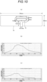
- Sample No. 3 A sample similar to Sample No. 1 was adopted as Sample No. 3 except that the interval 14d between the dipole antenna portion 14 and the loop conductive portion 13 was changed to 3 mm. Shapes of the conductive portions 13 and 14 of Sample No. 3: Fig. 10(a) .
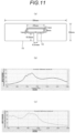
- Sample No. 4 A sample similar to Sample No. 1 was adopted as Sample No. 4 except that the dimensions (width 14b ⁇ length 14a) of the dipole antenna portion 14 were changed to 84 mm ⁇ 24 mm. Shapes of the conductive portions 13 and 14 of Sample No. 4 are illustrated in Fig. 11(a) .
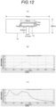
- Sample No. 5 A sample similar to Sample No. 1 was adopted as Sample No. 5 except that the dimensions (width 14b ⁇ length 14a) of the dipole antenna portion 14 were changed to 74 mm ⁇ 24 mm. Shapes of the conductive portions 13 and 14 of Sample No. 5 are illustrated in Fig. 12(a) .
- Base material 11 PET film having thickness of 38 um.
- Conductive portions 13, 14, and 131 aluminum having thickness of 10 ⁇ m.
- Shapes of conductive portions 13, 14, and 131 Similar to Fig. 7 .
- dipole antenna portion 14 width 14b ⁇ length 14a: 94 mm ⁇ 24 mm.
- Width 13w of loop conductive portion 13 1 mm.
- Interval 14d between dipole antenna portion and loop conductive portion 1 mm.
- connection conductive portions 131 one place.
- connection conductive portion 131 1 mm.
- Sample No. 7 A sample similar to Sample No. 6 was adopted as Sample No. 7 except that the width of the connection conductive portion 131 was changed to 22.03 mm. Shapes of the conductive portions 13 and 14 of Sample No. 7 are illustrated in Fig. 14(a) .
- Base material 11 PET film having thickness of 38 um.
- Conductive portions 13, 14, and 131 aluminum having thickness of 10 ⁇ m.
- Shapes of conductive portions 13, 14, and 131 Shapes of conductive portions 13, 14, and 131: Fig. 15(a) .
- dipole antenna portion 14 width 14b ⁇ length 14a: 94 mm ⁇ 24 mm.
- Width 13w of loop conductive portion 13 1 mm.
- Interval 14d between dipole antenna portion and loop conductive portion 1 mm.
- connection conductive portions 131 two places symmetrically with respect to first axis of symmetry.
- connection conductive portions 131 in horizontal direction 20.59 mm.
- Width of each connection conductive portion 131 1 mm.
- Sample No. 9 A sample similar to Sample No. 8 was adopted as Sample No. 9 except that the interval between the connection conductive portions 131 in the horizontal direction was changed to 15.00 mm. Shapes of the conductive portions 13 and 14 of Sample No. 9 are illustrated in Fig. 16(a) .
- Measurement results of sample Nos. 1 to 9 are illustrated in Figs. 8 to 16 , respectively.
- (a) illustrates the shapes of the conductive portions 13 and 14 of each sample
- (b) illustrates a graph of a measurement result for a tag alone (not affixed to the adherend)
- (c) illustrates a graph of a measurement result for a state in which the tag is affixed to a glass plate. From the measurement results, it was found that especially Sample No. 1 and Sample No. 6 are less affected by the adherend especially in a 900 MHz band including 920 MHz (dotted line position in the graph), which is a used frequency for UHF band RFID in Japan.
- Sample No. 1 described above and seal label-type RFID tags for the UHF band (Samples No. 10 and 11) described below were prepared, and installed in an anechoic box in various adherend affixing states (a. to i.) described below, and tagformance made by Voyantic Ltd was used to measure a communicable distance (theoretical read range forward) in a frequency range of 700 MHz to 1100 MHz. Note that measurement test conditions not described here were basically the same.
- a stacked structure is similar to that of Sample No. 1, a base material is PET, a conductive portion has a shape illustrated in Fig. 17(a) , antenna dimensions were width 92.5 mm ⁇ length 4.5 mm, and label dimensions were 98.5 mm ⁇ 7.5 mm.
- a stacked structure is similar to that of Sample No. 1, a base material is PET, a conductive portion has a shape illustrated in Fig. 17(b) , antenna dimensions were width 87 mm ⁇ length 18 mm, and label dimensions were 93 mm ⁇ 24 mm.
- Graphs of measurement results of Sample No. 1 and Sample Nos. 10 and 11 are illustrated in Figs. 18 and 19 .
- a graph of Fig. 18(a) is a measurement result of single tag (not affixed to the adherend) in case of above a
- a graph of Fig. 18(b) is a measurement result in an affixing state to Adherent b
- a graph of Fig. 18(c) is a measurement result in an affixing state to Adherent c
- PET bottle 2 liter type containing water a graph of Fig.
- a graph of Fig. 19(f) is a measurement result in an affixing state to Adherent f, glass plate
- a graph of Fig. 19(g) is a measurement result in an affixing state to Adherent g, PET plate
- a graph of Fig. 19(h) is a measurement result in an affixing state to Adherent h, PMMA plate
- a graph of Fig. 19(i) is a measurement result in an affixing state to Adherent i, double-sided corrugated board.
- Sample No. 1 described above and a seal label-type RFID tag for the UHF band (Sample No. 12) described below were prepared, and installed in an anechoic box in the above state (f.) of affixing the glass plate, and tagformance made by Voyantic Ltd was used to measure a communicable distance (theoretical read range forward) in a frequency range of 700 MHz to 1300 MHz.
- tagformance made by Voyantic Ltd was used to measure a communicable distance (theoretical read range forward) in a frequency range of 700 MHz to 1300 MHz.
- the same measurement was performed in the state (a.) of the single tag. Note that measurement test conditions not described here were basically the same.
- Sample No. 12 A sample similar to Sample No. 1 was adopted as Sample No. 12 except that a dimension of the inner peripheral edge of the dipole antenna portion 14 in a direction of the second axis of symmetry was changed to 60 mm, and the interval between the dipole antenna portion 14 and the loop conductive portion 13 was varied. Shapes of the conductive portions 13 and 14 of Sample No. 12 are illustrated in Fig. 20 .
- Sample No. 13 A sample similar to Sample No. 6 was adopted as Sample No. 13 except that a pair of connection conductive portions 131 is disposed on a side having the pair of tip edges 144 of the dipole antenna portion 14. Shapes of the conductive portions 13 and 14 of Sample No. 13 are illustrated in Fig. 21 .
- Graphs of measurement results of communicable distances of Samples No. 1 and No. 12 are illustrated in Fig. 22 . Further, in a simulation result of Sample No. 1, a graph of antenna impedance is illustrated in Fig. 23(a) , and a current distribution diagram is illustrated in Fig. 23(b) . Similarly, in a simulation result of Sample No. 12, a graph of antenna impedance is illustrated in Fig. 24(a) , and a current distribution diagram is illustrated in Fig. 24(b) . Similarly, in a simulation result of Sample No. 13, a graph of antenna impedance is illustrated in Fig. 25(a) , and a current distribution diagram is illustrated in Fig. 25(b) . Note that current distributions illustrated in Figs. 24(a) and 25(b) are based on color display, and in a region corresponding to the dipole antenna portion, as a current distribution becomes lower, generally darker color is displayed.
- the dipole antenna portion 14 surrounds the loop conductive portion 13 at a certain interval, and the connection conductive portion 131 is disposed on the opposite side from the side having the pair of tip edges 144 of the dipole antenna portion 14.
- the present invention is applicable to RFID tags in general.
- the present invention is suitable for a passive type (battery-free type) that uses electromagnetic waves received from a reader/writer as a drive power supply, and is also applicable to an active type (battery-mounted type) that incorporates a power source and a transmission circuit.
- the present invention is applicable not only to a label type (including both a seal type having a pressure sensitive adhesive layer on a back surface and a type having no pressure sensitive adhesive layer), but also various forms of RFID tags of a card type, a wristband type, etc.
Landscapes
- Engineering & Computer Science (AREA)
- Microelectronics & Electronic Packaging (AREA)
- Computer Hardware Design (AREA)
- Physics & Mathematics (AREA)
- General Physics & Mathematics (AREA)
- Theoretical Computer Science (AREA)
- Computer Networks & Wireless Communication (AREA)
- Details Of Aerials (AREA)
Abstract
Description
- The present invention relates to an RFID tag incorporating an inlay and a manufacturing method thereof.
- As is well known, an RFID tag (also referred to as an electronic tag, an IC tag, etc.) has an IC chip and an antenna connected thereto in order to store and read information without contact by short-range wireless communication. RFID (Radio frequency identification) is an automatic recognition system that uses such an RFID tag to write individual information of an object to the RFID tag and read individual information of an object stored in the RFID tag through wireless communication, and has been widely used for billing, prepaid, security management, article and logistics management, etc.
- Various types of RFID tags have been known, such as a card type, a label type (including both a seal type having a pressure sensitive adhesive layer on a back surface and a type having no pressure sensitive adhesive layer), and a wristband type. Of these types, some RFID tags such as label-type tags generally incorporate an inlay (inlet) in which a conductive portion including an antenna is formed on a resin film and an IC chip is disposed on this conductive portion.
- As an RFID tag incorporating such an inlay, for example, one described in
Patent Literature 1 has been known. - However, in the RFID tag described in
Patent Literature 1, since an antenna is not formed in the inlay, and the RFID tag is configured by stacking the inlay on an antenna portion formed separately from the inlay, there have been problems in that manufacturing efficiency is low, and the thickness of the whole including the antenna could not be suppressed. Since the thickness of the inlay affects the thickness of the RFID tag, a thinner one is preferable. - Patent Literature 1:
JP 2008-107947 A - Accordingly, it is a primary object of the present invention to provide an RFID tag including an inlay that is thin and easy to manufacture.
- An RFID tag that solves the above problem is as follows.
- An RFID tag including
- a base material having a main surface; and
- an inlay provided with an IC chip and an antenna on the base material, wherein
- the antenna includes a loop conductive portion having both end portions connected to the IC chip so as to form a loop shape through the IC chip, and a dipole antenna portion disposed to surround the loop conductive portion with an interval allowing inductive coupling, and
- the loop conductive portion and the dipole antenna portion are formed on the main surface to have same thickness based on the main surface, and the IC chip is disposed on both end portions of the loop conductive portion.
- According to the RFID tag, the loop conductive portion and the dipole antenna portion can be easily formed in one process, so that the thickness of the inlay can be suppressed when compared to that described in
Patent Literature 1 while improving the manufacturing efficiency, and thus the thickness of the RFID tag can be suppressed. - An RFID tag including
- a base material having a main surface; and
- an inlay provided with an IC chip and an antenna on the base material, wherein
- the antenna includes a loop conductive portion having both end portions connected to the IC chip so as to form a loop shape through the IC chip, and a dipole antenna portion disposed to surround the loop conductive portion with an interval,
- the loop conductive portion extends through the IC chip so as to have a relatively short first axis of symmetry and a relatively long second axis of symmetry orthogonal thereto,
- the dipole antenna portion forms a shape having an axis of symmetry overlapping the first axis of symmetry,
- the IC chip is disposed at one end portion of the first axis of symmetry,
- a single connection conductive portion is provided to connect the other end portion of the first axis of symmetry of the loop conductive portion and the dipole antenna portion to each other, and
- the loop conductive portion, the connection conductive portion, and the dipole antenna portion are formed on the main surface so as to have same thickness based on the main surface, and the IC chip is disposed at both end portions of the loop conductive portion.
- According to the RFID tag, the loop conductive portion and the dipole antenna portion can be easily formed in one process, so that the thickness of the inlay can be suppressed when compared to that described in
Patent Literature 1 while improving the manufacturing efficiency, and thus the thickness of the RFID tag can be suppressed. - The RFID tag according to the first or second aspect, wherein
- the dipole antenna portion is disposed to surround the loop conductive portion at a certain interval,
- the loop conductive portion extends through the IC chip to form an oval shape or a substantially rectangular shape having a relatively short first axis of symmetry and a relatively long second axis of symmetry orthogonal thereto,
- the IC chip is disposed at one end portion of the first axis of symmetry, and
- the dipole antenna portion has an axis of symmetry overlapping the first axis of symmetry, has a pair of tip edges facing and spaced apart from each other with a virtual line obtained by extending an IC chip side of the first axis of symmetry interposed therebetween, and continues so as to wrap around the loop conductive portion from one side to the other side of each of the tip edges.
- In an RFID tag, it is preferable that the antenna is in a wide bandwidth since an influence of shift of a frequency band due to a surrounding environment, etc. is reduced. By adopting the shape and arrangement of the dipole antenna portion and arrangement of the IC chip of this aspect, it is possible to widen a bandwidth of the antenna while suppressing a decrease in communication distance. Even though a reason therefor is not clear, one reason is considered that the dipole antenna portion is evenly inductively coupled with the loop conductive portion entirely in a circumferential direction.
- The RFID tag according to the third aspect, wherein
- the dipole antenna portion has an inner peripheral edge continuous along an outer peripheral edge of the loop conductive portion, outer peripheral edges, and the pair of tip edges connecting both ends of the inner peripheral edge and both ends of each of the outer peripheral edges,
- the outer peripheral edges have a pair of first edge portions extending parallel to the first axis of symmetry, a second edge portion extending parallel to the second axis of symmetry and connecting one end of one of the first edge portions and one end of the other one of the first edge portions, and a third edge portion connecting ends of the pair of tip edges on an opposite side from a second edge portion side and the other end of each of the first edge portions, and
- a sum of a dimension of the pair of first edge portions in a direction along the first axis of symmetry, a dimension of the second edge portion in a direction along the second axis of symmetry, and a dimension of the pair of tip edges in the direction along the first axis of symmetry is equal to 1/2 wavelength of a used frequency.
- As will be apparent from embodiments to be described later, it is preferable in terms of widening the bandwidth of the antenna when the dimensions and shapes of the respective portions are within the ranges of this aspect.
- The RFID tag according to the fourth aspect, wherein the used frequency is in a UHF band.
- In general, in an RFID, four types of used frequency bands are used, namely an LF band, an HF band, a UHF band, and a microwave band. Of these types, the UHF band (860 to 960 MHz), which is the used frequency of the fifth aspect, has a high frequency and a short wavelength, which is advantageous for miniaturizing antennas. On the other hand, depending on the shape of the antenna, it may be difficult to achieve both miniaturization and performance, or easiness of manufacture may be impaired. On the other hand, adopting the antenna shape of the third aspect described above as in this fifth aspect is preferable since the antenna shape is not only simple and easy to manufacture, but also can achieve both miniaturization and performance.
- The RFID tag according to any one of the third to fifth aspects, wherein the RFID tag is an RFID label having a pressure sensitive adhesive layer on a back surface.
- The bandwidth of the antenna of the RFID label affixed to an article by the pressure sensitive adhesive layer on the back side shifts due to an influence of a dielectric constant of the article to be affixed. Therefore, in an article affixing-type RFID tag, when the shape of the dipole antenna of the second aspect is adopted to widen the bandwidth, even if the bandwidth of the antenna shifts somewhat, the used frequency rarely deviates from the antenna bandwidth, and communication performance such as a communication distance is less likely to deteriorate, which is preferable.
- The RFID tag according to any one of the first to sixth aspects, wherein the loop conductive portion has a dimension at which a resonance circuit configured together with the IC chip is tuned to a used frequency.
- When the loop conductive portion has the dimension of this aspect, by staggered tuning of a resonance circuit including the IC chip and the loop conductive portion and a resonance circuit including the IC chip, the loop conductive portion, and the dipole antenna portion, it is possible to widen the bandwidth of the antenna, which is preferable.
- A method of manufacturing the RFID tag according to the first aspect, the method including
- forming the loop conductive portion and the dipole antenna portion on the base material by etching or printing, and
- mounting the IC chip on the loop conductive portion.
- The same effects as those of the first aspect are obtained.
- The present invention provides an advantage such as an RFID tag including an inlay that is thin and easy to manufacture.
-
-
Fig. 1 is a front view illustrating an example of an RFID tag. -
Fig. 2 is a back view illustrating the example of the RFID tag. -
Fig. 3 is a cross-sectional view taken along 3-3 ofFig. 1 . -
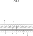
Fig. 4 is a cross-sectional view corresponding to a cross section 3-3 ofFig. 1 . -
Fig. 5 is a plan view illustrating an enlarged main part of a loop conductive portion/dipole antenna portion. -
Fig. 6 is a plan view illustrating an enlarged main part of the loop conductive portion/dipole antenna portion. -
Fig. 7 is a plan view illustrating an enlarged main part of the loop conductive portion/dipole antenna portion. -
Fig. 8 is a diagram illustrating an example of a shape of a conductive portion, and a graph illustrating test results thereof. -
Fig. 9 is a diagram illustrating an example of a shape of the conductive portion, and a graph illustrating test results thereof. -
Fig. 10 is a diagram illustrating an example of a shape of the conductive portion, and a graph illustrating test results thereof. -
Fig. 11 is a diagram illustrating an example of a shape of the conductive portion, and a graph illustrating test results thereof. -
Fig. 12 is a diagram illustrating an example of a shape of the conductive portion, and a graph illustrating test results thereof. -
Fig. 13 is a diagram illustrating an example of a shape of the conductive portion, and a graph illustrating test results thereof. -
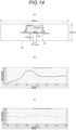
Fig. 14 is a diagram illustrating an example of a shape of the conductive portion, and a graph illustrating test results thereof. -
Fig. 15 is a diagram illustrating an example of a shape of the conductive portion, and a graph illustrating test results thereof. -
Fig. 16 is a diagram illustrating an example of a shape of the conductive portion, and a graph illustrating test results thereof. -
Fig. 17 is a plan view illustrating a shape of a conductive portion of a commercial product. -
Fig. 18 is a graph illustrating test results. -
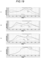
Fig. 19 is a graph illustrating test results. -
Fig. 20 is a plan view illustrating a shape example of the conductive portion. -
Fig. 21 is a plan view illustrating a shape example of the conductive portion. -
Fig. 22 is a graph illustrating test results. -
Fig. 23 is a diagram illustrating a simulation result. -
Fig. 24 is a diagram illustrating a simulation result. -
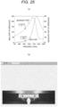
Fig. 25 is a diagram illustrating a simulation result. - An example of an
RFID tag 10 will be described in detail below with reference to the accompanying drawings. As illustrated inFigs. 1 to 3 , theRFID tag 10 of this example includes aninlay 15 in which anIC chip 12 andconductive portions base material 11 having a sheet shape, etc. Dimensions and shape of theinlay 15 may be the same as those of theRFID tag 10 or may be different from (for example, smaller than) theRFID tag 10. Since an example illustrated inFig. 2 is a seal label-type RFID using thebase material 11 made of resin, a pressure sensitiveadhesive layer 16 is provided on a back surface side of thebase material 11 so as to cover theconductive portions IC chip 12, and apeel sheet 17 is provided to cover the pressure sensitiveadhesive layer 16. By peeling off thepeel sheet 17 and exposing the pressure sensitiveadhesive layer 16 on the back surface, theRFID tag 10 can be affixed to an adherend such as a PET bottle. Meanwhile, a front surface side of thebase material 11 is covered with apaper layer 18 as a printing portion. Thepaper layer 18 is attached to a surface of thebase material 11 via anadhesive layer 19. - In
Fig. 4 , thebase material 11 is a paper layer that also serves as a printing portion, and the number of portions required is smaller than that illustrated inFig. 3 . - A material of the
base material 11 of theinlay 15 is not particularly limited. However, it is possible to use synthetic resin such as polyethylene terephthalate, polyvinyl chloride, polyester, polyethylene, or polypropylene, and it is also possible to use paper such as high-quality paper, medium-quality paper, coated paper, art paper, or kraft paper. A thickness of the sheet-shapedbase material 11 can be determined as appropriate, and is usually preferably set to 25 to 50 um. Thebase material 11 has dimensions that allow mounting of components (theIC chip 12, theconductive portions base material 11 is transparent or translucent, a back view appears symmetrically with a front view, and when thebase material 11 is opacity, components such as theIC chip 12 and theconductive portions - The
conductive portions base material 11 by a known method. For example, theconductive portions base material 11 using plating, vapor deposition, dry lamination, etc., printing a resist pattern on the metal layer, and then performing chemical etching. Alternatively, theconductive portions base material 11. A thickness of theconductive portions - As can be seen from the above description, depending on the form of the
RFID tag 10, a material of theconductive portions inlay 15, etc. change. - The antenna of the
RFID tag 10 of this example includes a loopconductive portion 13 having both end portions connected to theIC chip 12 so as to form a loop shape through theIC chip 12, and adipole antenna portion 14 disposed to surround the loopconductive portion 13 with an interval allowing inductive coupling, the loopconductive portion 13 and thedipole antenna portion 14 are formed on the back surface (or the front surface) of thebase material 11 so as to have a common thickness, and theIC chip 12 is disposed on both end portions of the loopconductive portion 13. As a result, the loopconductive portion 13 and thedipole antenna portion 14 can be easily formed in one process, so that the thickness of theinlay 15 can be suppressed while improving the manufacturing efficiency, and thus the thickness of theRFID tag 10 can be suppressed. - A shape of the loop
conductive portion 13 can be determined as appropriate. However, as in the illustrated example, it is preferable to adopt a shape having a relatively short first axis ofsymmetry 13y and a relatively long second axis ofsymmetry 13x orthogonal thereto, and it is particularly preferable to adopt an oval shape (seeFig. 5 , etc.) or a substantially rectangular shape (seeFig. 6 ). Note that the oval shape includes both a shape having one or a plurality of straight line parts (a shape having a pair of parallel straight line parts having the same length and semicircular parts connecting both ends of these straight light parts in the illustrated example) and a shape not including a straight line part such as an ellipse. Further, the substantially rectangular shape includes not only a shape having right-angled corners as illustrated inFig. 6 , but also a rounded rectangle having mostly straight four sides and quarter-circular corners. - A position of the
IC chip 12 can be determined as appropriate. However, as in the illustrated example, theIC chip 12 is preferably disposed at one end portion of the first axis ofsymmetry 13y when the loopconductive portion 13 has the relatively short first axis ofsymmetry 13y and the relatively long second axis ofsymmetry 13x orthogonal thereto. - An
interval 14d between thedipole antenna portion 14 and the loopconductive portion 13 can be determined as appropriate. However, as in the illustrated example, it is preferable that thedipole antenna portion 14 is disposed almost entirely so as to surround the loopconductive portion 13 at thecertain interval 14d. Thisinterval 14d depends on the dimensions of the loopconductive portion 13, and can be normally set to about 0.5 to 1.5 mm. - In addition, a shape of the
dipole antenna portion 14 can be determined as appropriate. However, as in the illustrated example, when the loopconductive portion 13 has the relatively short first axis ofsymmetry 13y and the relatively long second axis ofsymmetry 13x orthogonal thereto, it is preferable that thedipole antenna portion 14 has an axis of symmetry overlapping the first axis ofsymmetry 13y, has a pair of tip edges 144 facing each other at an interval with a virtual line obtained by extending theIC chip 12 side of the first axis ofsymmetry 13y interposed therebetween, and continues in a substantially C-shape so as to wrap around the loopconductive portion 13 from one side to the other side of each of the tip edges 144. Aninterval 14e between the pair of tip edges 144 in a direction along the second axis ofsymmetry 13x can be determined as appropriate, and can be normally set to about 1 to 7 mm. Outerperipheral edges 141 to 143 of thedipole antenna portion 14 may be formed parallel to an innerperipheral edge 145 of thedipole antenna portion 14, or may be formed along (particularly parallel to) an outer peripheral shape (for example, rectangle) of theinlay 15 regardless of the innerperipheral edge 145 of thedipole antenna portion 14. - By adopting the shape and arrangement of the
dipole antenna portion 14 and arrangement of theIC chip 12 described above, it is possible to widen a bandwidth of the antenna while suppressing a decrease in communication distance. Even though a reason therefor is not clear, one reason is considered that thedipole antenna portion 14 is evenly inductively coupled with the loopconductive portion 13 entirely in a circumferential direction. - Since the loop
conductive portion 13 has inductance and resistance, the dimensions of each portion (a loop area, a circumference length, aline width 13w, etc.) can be appropriately determined according to the required inductance and resistance of the loopconductive portion 13. The inductance of the loopconductive portion 13 can be used to compensate for lack of a reactance component in impedance matching between the IC and thedipole antenna portion 14. In addition, the inductance of the loopconductive portion 13 can be used to tune a resonance circuit configured together with theIC chip 12 to a used frequency. In this case, by staggered tuning of a resonance circuit including theIC chip 12 and the loopconductive portion 13 and a resonance circuit including theIC chip 12, the loopconductive portion 13, and thedipole antenna portion 14, it is possible to widen the bandwidth of the antenna (widen the bandwidth to a low frequency side by increasing the circumference length of the loop conductive portion 13). As an example, when the used frequency is in a UHF band, the loop area (area inside the loop) of the loopconductive portion 13 can be about 60 to 110 mm2. Further, an inner circumference length of a loop of the loopconductive portion 13 can be set to about 45 to 55 mm. Furthermore, theline width 13w of the loopconductive portion 13 can be set to about 0.5 to 3.0 mm. - Dimensions of each portion of the
dipole antenna portion 14 can be appropriately determined based on 1/2 wavelength of the used frequency. For example, thedipole antenna portion 14 in the illustrated example has the outerperipheral edges 141 to 143, the innerperipheral edge 145 continuous along an outer peripheral edge of the loopconductive portion 13, and the pair of tip edges 144 connecting both ends of the innerperipheral edge 145 and both ends of each of the outerperipheral edges 141 to 143, and the outerperipheral edges 141 to 143 have a pair offirst edge portions 141 extending parallel to the first axis ofsymmetry 13y, asecond edge portion 142 extending parallel to the second axis ofsymmetry 13x and connecting one end of one of thefirst edge portions 141 and one end of the other one of thefirst edge portions 141, and athird edge portion 143 connecting ends of the pair of tip edges 144 on the opposite side from thesecond edge portion 142 side and the other end of each of thefirst edge portions 141. In this case, when a sum of adimension 14a of the pair offirst edge portions 141 in a direction along the first axis ofsymmetry 13y, adimension 14b of thesecond edge portion 142 in a direction along the second axis ofsymmetry 13x, and adimension 14c of the pair of tip edges 144 in the direction along the first axis ofsymmetry 13y is equal to 1/2 wavelength of the used frequency, it is preferable for widening the bandwidth of the antenna. - The
RFID tag 10 of this example can be applied to any of four types of commonly used frequency bands, namely an LF band, an HF band, a UHF band, and a microwave band. Of these types, the UHF band (860 to 960 MHz) has a high frequency and a short wavelength, which is advantageous for miniaturizing antennas. On the other hand, depending on the shape of the antenna, it may be difficult to achieve both miniaturization and performance, or easiness of manufacture may be impaired. Therefore, the dimensions, arrangement, and shape of thedipole antenna portion 14 and the loopconductive portion 13 in the wide bandwidth described above are particularly suitable for use in the UHF band. When thedipole antenna portion 14 in the illustrated example is used in the UHF band, for example, it is preferable that a length of the pair offirst edge portions 141 is set to about 20 to 27 mm, a length of thesecond edge portion 142 is set to about 91 to 97 mm, and a length of each of the pair of tip edges 144 is set to about 7.5 to 13.5 mm. In addition, aminimum width 14w of thedipole antenna portion 14 can be set to about 2.5 to 8.5 mm. - The
RFID tag 10 may be in a form other than the seal label type of this example, and the dimensions, arrangement, and shape of thedipole antenna portion 14 and the loopconductive portion 13 of this example can be applied to a form other than the seal label type. However, since the bandwidth of the antenna of the seal label-type RFID tag shifts due to an influence of a dielectric constant of an object to be affixed, when the dimensions and arrangement of thedipole antenna portion 14 and the loopconductive portion 13 in the wide bandwidth described above are adopted to broaden the bandwidth, even if the bandwidth of the antenna shifts to some extent, the used frequency is less likely to deviate from the antenna bandwidth, and communication performance such as communication distance is less likely to deteriorate, which is preferable. - In the above example, a conductive portion connecting the loop
conductive portion 13 and thedipole antenna portion 14 is not provided. However, as illustrated inFig. 7 , when the loopconductive portion 13 extends through theIC chip 12 so as to have the relatively short first axis ofsymmetry 13y and the relatively long second axis ofsymmetry 13x orthogonal thereto, thedipole antenna portion 14 forms a shape having the axis ofsymmetry 14y overlapping the first axis ofsymmetry 13y, and theIC chip 12 is disposed at the one end portion of the first axis ofsymmetry 13y, a single connectionconductive portion 131 that connects the other end portion of the first axis ofsymmetry 13y of the loopconductive portion 13 and thedipole antenna portion 14 may be provided. In this case, it is preferable that the connectionconductive portion 131 is disposed on the opposite side from a side having the pair of tip edges 144 of thedipole antenna portion 14. - A width of the connection
conductive portion 131 can be determined as appropriate, and can be within a similar range to that of theline width 13w of the loopconductive portion 13, for example. In particular, it is preferable that the width of the connectionconductive portion 131 is equal to or less than theinterval 14e between the pair of tip edges 144 of thedipole antenna portion 14. Other points in the case of having the connectionconductive portion 131 are basically similar to those in the case of not having the connectionconductive portion 131. - Seal label-type RFID tags for the UHF band (Samples No. 1 to 9) described below were prepared, and installed in an anechoic box in a state of being affixed to an approximate center of a glass plate (soda glass,
width 100 mm ×length 150 mm ×thickness 10 mm) and in a state of a single unit without affixing, and tagformance made by Voyantic Ltd was used to measure a communicable distance (theoretical read range forward) in a frequency range of 700 MHz to 1300 MHz. Note that measurement test conditions not described here were basically the same. - Stacked structure: similar to that of
Fig. 3 . - Base material 11: PET film having thickness of 38 um.
-
Conductive portions 13 and 14: aluminum having thickness of 10 µm. - Shape of conductive portion:
Fig. 8(a) . Similar toFigs. 1 ,2 , and5 . - Dimensions of dipole antenna portion 14 (
width 14b ×length 14a): 94 mm × 24 mm. - Dimensions of loop conductive portion 13 (
width 13b ×length 13a): 24 mm × 6 mm. - Loop area of loop conductive portion 13: 84.56 mm2.
- Loop outer circumference length of loop conductive portion 13: 54.84 mm.
- Loop inner circumference length of loop conductive portion 13: 48.56 mm.
-
Width 13w of loop conductive portion 13: 1 mm. -
Interval 14d between dipole antenna portion and loop conductive portion: 1 mm. - Impedance (866 MHz) of IC chip 12: 15j265 (Ω)
- (915MHz):14j252(Ω)
- (915MHz):13j242(Ω)
- A sample similar to Sample No. 1 was adopted as Sample No. 2 except that the
interval 14d between thedipole antenna portion 14 and the loopconductive portion 13 was changed to 2 mm. Shapes of theconductive portions Fig. 9(a) . - A sample similar to Sample No. 1 was adopted as Sample No. 3 except that the
interval 14d between thedipole antenna portion 14 and the loopconductive portion 13 was changed to 3 mm. Shapes of theconductive portions Fig. 10(a) . - A sample similar to Sample No. 1 was adopted as Sample No. 4 except that the dimensions (
width 14b ×length 14a) of thedipole antenna portion 14 were changed to 84 mm × 24 mm. Shapes of theconductive portions Fig. 11(a) . - A sample similar to Sample No. 1 was adopted as Sample No. 5 except that the dimensions (
width 14b ×length 14a) of thedipole antenna portion 14 were changed to 74 mm × 24 mm. Shapes of theconductive portions Fig. 12(a) . - Stacked structure: similar to that of
Fig. 3 . - Base material 11: PET film having thickness of 38 um.
-
Conductive portions - Shapes of
conductive portions Fig. 13(a) . Similar toFig. 7 . - Dimensions of dipole antenna portion 14 (
width 14b ×length 14a): 94 mm × 24 mm. - Dimensions of loop conductive portion 13 (
width 13b ×length 13a): 24 mm × 6 mm. -
Width 13w of loop conductive portion 13: 1 mm. -
Interval 14d between dipole antenna portion and loop conductive portion: 1 mm. - Number of connection conductive portions 131: one place.
- Width of connection conductive portion 131: 1 mm.
- A sample similar to Sample No. 6 was adopted as Sample No. 7 except that the width of the connection
conductive portion 131 was changed to 22.03 mm. Shapes of theconductive portions Fig. 14(a) . - Stacked structure: similar to that of
Fig. 3 . - Base material 11: PET film having thickness of 38 um.
-
Conductive portions - Shapes of
conductive portions Fig. 15(a) . - Dimensions of dipole antenna portion 14 (
width 14b ×length 14a): 94 mm × 24 mm. - Dimensions of loop conductive portion 13 (
width 13b ×length 13a): 24 mm × 6 mm. -
Width 13w of loop conductive portion 13: 1 mm. -
Interval 14d between dipole antenna portion and loop conductive portion: 1 mm. - Number of connection conductive portions 131: two places symmetrically with respect to first axis of symmetry.
- Interval between connection
conductive portions 131 in horizontal direction: 20.59 mm. - Width of each connection conductive portion 131: 1 mm.
- A sample similar to Sample No. 8 was adopted as Sample No. 9 except that the interval between the connection
conductive portions 131 in the horizontal direction was changed to 15.00 mm. Shapes of theconductive portions Fig. 16(a) . - Measurement results of sample Nos. 1 to 9 are illustrated in
Figs. 8 to 16 , respectively. Note that in each figure, (a) illustrates the shapes of theconductive portions interval 14d between thedipole antenna portion 14 and the loopconductive portion 13 is excessively wide, or a connection width is excessively wide in the case of providing the connection conductive portion, a preferable result cannot be obtained. - Sample No. 1 described above and seal label-type RFID tags for the UHF band (Samples No. 10 and 11) described below were prepared, and installed in an anechoic box in various adherend affixing states (a. to i.) described below, and tagformance made by Voyantic Ltd was used to measure a communicable distance (theoretical read range forward) in a frequency range of 700 MHz to 1100 MHz. Note that measurement test conditions not described here were basically the same.
- A commercially available RFID label SPMU9204 manufactured by DAIO ENGINEERING Co., ltd. was used. This RFID label corresponds to the UHF band. In the RFID label, a stacked structure is similar to that of Sample No. 1, a base material is PET, a conductive portion has a shape illustrated in
Fig. 17(a) , antenna dimensions were width 92.5 mm × length 4.5 mm, and label dimensions were 98.5 mm × 7.5 mm. - A commercially available RFID label SPMU8718 manufactured by DAIO ENGINEERING Co., ltd. was used. This RFID label corresponds to the UHF band. In the RFID label, a stacked structure is similar to that of Sample No. 1, a base material is PET, a conductive portion has a shape illustrated in
Fig. 17(b) , antenna dimensions were width 87 mm ×length 18 mm, and label dimensions were 93 mm × 24 mm. -
- a. None (state of single tag)
- b. PET bottle containing water (500 ml type, affixing position: center of side surface in height direction)
- c. PET bottle containing water (2 liter type, affixing position: center of side surface in height direction)
- d. Drip bag containing water (1 liter type, affixing position: center of front surface)
- e. Shochu bottle 900 ml (unopened, affixing position: center of side surface in height direction)
- f. Glass plate (
length 100 mm ×width 150 mm ×thickness 10 mm, affixing position: center) - g. PET plate (
length 100 mm ×width 150 mm ×thickness 10 mm, affixing position: center) - h. PMMA plate (
length 100 mm ×width 150 mm ×thickness 10 mm, affixing position: center) - i. Double-sided corrugated board (
length 100 mm ×width 150 mm ×thickness 5 mm, affixing position: center) - Graphs of measurement results of Sample No. 1 and Sample Nos. 10 and 11 are illustrated in
Figs. 18 and19 . Note that a graph ofFig. 18(a) is a measurement result of single tag (not affixed to the adherend) in case of above a, a graph ofFig. 18(b) is a measurement result in an affixing state to Adherent b, PET bottle 500 ml containing water, a graph ofFig. 18(c) is a measurement result in an affixing state to Adherent c, PET bottle 2 liter type containing water, a graph ofFig. 18(d) is a measurement result in an affixing state to Adherent d, drip bag containing water, and a graph ofFig. 18(e) is a measurement result in an affixing state to Adherent e, Japanese Sake bottle. In addition, a graph ofFig. 19(f) is a measurement result in an affixing state to Adherent f, glass plate, a graph ofFig. 19(g) is a measurement result in an affixing state to Adherent g, PET plate, a graph ofFig. 19(h) is a measurement result in an affixing state to Adherent h, PMMA plate, and a graph ofFig. 19(i) is a measurement result in an affixing state to Adherent i, double-sided corrugated board. - From the measurement results, it was found that especially Sample No. 1 is less affected by the adherend and has excellent properties when compared to commercial product Samples Nos. 10 and 11, especially in a 900 MHz band including 920 MHz (dotted line position in the graph), which is a used frequency for UHF band RFID in Japan.
- Sample No. 1 described above and a seal label-type RFID tag for the UHF band (Sample No. 12) described below were prepared, and installed in an anechoic box in the above state (f.) of affixing the glass plate, and tagformance made by Voyantic Ltd was used to measure a communicable distance (theoretical read range forward) in a frequency range of 700 MHz to 1300 MHz. In addition, for sample No. 12, the same measurement was performed in the state (a.) of the single tag. Note that measurement test conditions not described here were basically the same.
- A sample similar to Sample No. 1 was adopted as Sample No. 12 except that a dimension of the inner peripheral edge of the
dipole antenna portion 14 in a direction of the second axis of symmetry was changed to 60 mm, and the interval between thedipole antenna portion 14 and the loopconductive portion 13 was varied. Shapes of theconductive portions Fig. 20 . - Furthermore, with respect to antenna shapes of Sample Nos. 1 and 12 described above and Sample No. 13 described below, the impedance and current distribution of each antenna were evaluated using a 3D planar electromagnetic field simulator manufactured by Sonnet Software, Inc.
- A sample similar to Sample No. 6 was adopted as Sample No. 13 except that a pair of connection
conductive portions 131 is disposed on a side having the pair of tip edges 144 of thedipole antenna portion 14. Shapes of theconductive portions Fig. 21 . - Graphs of measurement results of communicable distances of Samples No. 1 and No. 12 are illustrated in
Fig. 22 . Further, in a simulation result of Sample No. 1, a graph of antenna impedance is illustrated inFig. 23(a) , and a current distribution diagram is illustrated inFig. 23(b) . Similarly, in a simulation result of Sample No. 12, a graph of antenna impedance is illustrated inFig. 24(a) , and a current distribution diagram is illustrated inFig. 24(b) . Similarly, in a simulation result of Sample No. 13, a graph of antenna impedance is illustrated inFig. 25(a) , and a current distribution diagram is illustrated inFig. 25(b) . Note that current distributions illustrated inFigs. 24(a) and25(b) are based on color display, and in a region corresponding to the dipole antenna portion, as a current distribution becomes lower, generally darker color is displayed. - It was found from results illustrated in
Figs. 22 to 24 that, when the interval between thedipole antenna portion 14 and the loopconductive portion 13 is not constant, a current distribution of thedipole antenna portion 14 is lowered, and a resonance frequency is shifted to a low frequency side to decrease a communicable distance in a state of affixing the glass. In particular, from the result ofFig. 22 , it was presumed that when the area of thedipole antenna portion 14 becomes small, an influence of the adherend is likely to increase. In addition, it can be understood that, when frequency characteristics of the impedance of the entire antenna (the loopconductive portion 13 and the dipole antenna portion 14) are designed to match frequency characteristics of the impedance of theIC chip 12, attenuation of power is be reduced, and a communication distance is extended. Furthermore, it was found from the results illustrated inFigs. 23 and25 that, when the connectionconductive portion 131 is disposed on the side having the pair of tip edges 144 of thedipole antenna portion 14, a resonance frequency shifts to the high frequency side. From the above description, it was found to be particularly preferable when thedipole antenna portion 14 surrounds the loopconductive portion 13 at a certain interval, and the connectionconductive portion 131 is disposed on the opposite side from the side having the pair of tip edges 144 of thedipole antenna portion 14. - The present invention is applicable to RFID tags in general. In other words, the present invention is suitable for a passive type (battery-free type) that uses electromagnetic waves received from a reader/writer as a drive power supply, and is also applicable to an active type (battery-mounted type) that incorporates a power source and a transmission circuit. In addition, the present invention is applicable not only to a label type (including both a seal type having a pressure sensitive adhesive layer on a back surface and a type having no pressure sensitive adhesive layer), but also various forms of RFID tags of a card type, a wristband type, etc.
-
- 10
- RFID tag
- 11
- Base material
- 12
- IC chip
- 13, 14
- Conductive portion
- 15
- Inlay
- 16
- Pressure sensitive adhesive layer
- 17
- Peel sheet
- 18
- Paper layer
- 19
- Adhesive layer
- 13
- Loop conductive portion
- 13y
- First axis of symmetry
- 13x
- Second axis of symmetry
- 14
- Dipole antenna portion
- Connection conductive portion
- 131
- 141 to 143
- Outer peripheral edge
- 141
- First edge portion
- 142
- Second edge portion
- 143
- Third edge portion
- 144
- Tip edge
- 145
- Inner peripheral edge
Claims (8)
- An RFID tag comprising:a base material having a main surface; andan inlay provided with an IC chip and an antenna on the base material,wherein:the antenna includes a loop conductive portion having both end portions connected to the IC chip so as to form a loop shape through the IC chip, and a dipole antenna portion disposed to surround the loop conductive portion with an interval allowing inductive coupling; andthe loop conductive portion and the dipole antenna portion are formed on the main surface to have same thickness, and the IC chip is disposed on the both end portions of the loop conductive portion.
- An RFID tag comprising:a base material having a main surface; andan inlay provided with an IC chip and an antenna on the base material,wherein:the antenna includes a loop conductive portion having both end portions connected to the IC chip so as to form a loop shape through the IC chip, and a dipole antenna portion disposed to surround the loop conductive portion with an interval;the loop conductive portion extends through the IC chip so as to have a relatively short first axis of symmetry and a relatively long second axis of symmetry orthogonal thereto;the dipole antenna portion forms a shape having an axis of symmetry overlapping the first axis of symmetry;the IC chip is disposed at one end portion of the first axis of symmetry;a single connection conductive portion is provided to connect the other end portion of the first axis of symmetry of the loop conductive portion and the dipole antenna portion to each other; andthe loop conductive portion, the connection conductive portion, and the dipole antenna portion are formed on the main surface so as to have same thickness, and the IC chip is disposed on both end portions of the loop conductive portion.
- The RFID tag according to claim 1 or 2, whereinthe dipole antenna portion is disposed to surround the loop conductive portion at a certain interval,the loop conductive portion extends through the IC chip to form an oval shape or a substantially rectangular shape having a relatively short first axis of symmetry and a relatively long second axis of symmetry orthogonal thereto,the IC chip is disposed at one end portion of the first axis of symmetry, andthe dipole antenna portion has an axis of symmetry overlapping the first axis of symmetry, has a pair of tip edges facing and spaced apart from each other with a virtual line obtained by extending an IC chip side of the first axis of symmetry interposed therebetween, and continues so as to wrap around the loop conductive portion from one side to the other side of each of the tip edges.
- The RFID tag according to claim 3, wherein:the dipole antenna portion has an inner peripheral edge continuous along an outer peripheral edge of the loop conductive portion, outer peripheral edges, and the pair of tip edges connecting both ends of the inner peripheral edge and both ends of each of the outer peripheral edges;the outer peripheral edges have a pair of first edge portions extending parallel to the first axis of symmetry, a second edge portion extending parallel to the second axis of symmetry and connecting one end of one of the first edge portions and one end of the other one of the first edge portions, and a third edge portion connecting ends of the pair of tip edges on an opposite side from a second edge portion side and the other end of each of the first edge portions; anda sum of a dimension of the pair of first edge portions in a direction along the first axis of symmetry, a dimension of the second edge portion in a direction along the second axis of symmetry, and a dimension of the pair of tip edges in the direction along the first axis of symmetry is equal to 1/2 wavelength of a used frequency.
- The RFID tag according to claim 4, wherein
the used frequency is in a UHF band. - The RFID tag according to any one of claims 3 to 5, wherein
the RFID tag is an RFID label having a pressure sensitive adhesive layer on a back surface. - The RFID tag according to any one of claims 1 to 6, wherein
the loop conductive portion has a dimension at which a resonance circuit configured together with the IC chip is tuned to a used frequency. - A method of manufacturing the RFID tag according to claim 1, the method comprising:forming the loop conductive portion and the dipole antenna portion on the base material by etching or printing; andmounting the IC chip on the loop conductive portion.
Applications Claiming Priority (2)
| Application Number | Priority Date | Filing Date | Title |
|---|---|---|---|
| JP2020209378A JP7587979B2 (en) | 2020-12-17 | 2020-12-17 | RFID tag and its manufacturing method |
| PCT/JP2021/045844 WO2022131215A1 (en) | 2020-12-17 | 2021-12-13 | Rfid tag and manufacturing method thereof |
Publications (2)
| Publication Number | Publication Date |
|---|---|
| EP4266213A1 true EP4266213A1 (en) | 2023-10-25 |
| EP4266213A4 EP4266213A4 (en) | 2024-11-13 |
Family
ID=82059444
Family Applications (1)
| Application Number | Title | Priority Date | Filing Date |
|---|---|---|---|
| EP21906577.8A Pending EP4266213A4 (en) | 2020-12-17 | 2021-12-13 | Rfid tag and manufacturing method thereof |
Country Status (6)
| Country | Link |
|---|---|
| US (1) | US12431609B2 (en) |
| EP (1) | EP4266213A4 (en) |
| JP (1) | JP7587979B2 (en) |
| CN (1) | CN116458012A (en) |
| TW (1) | TWI891950B (en) |
| WO (1) | WO2022131215A1 (en) |
Families Citing this family (11)
| Publication number | Priority date | Publication date | Assignee | Title |
|---|---|---|---|---|
| EP3971776A1 (en) * | 2020-09-18 | 2022-03-23 | Becton Dickinson France | Medical container comprising an rfid tag for remote identification |
| JP7651373B2 (en) * | 2021-05-24 | 2025-03-26 | Tdk株式会社 | Antenna device and wireless power transmission device including same |
| JP7412810B1 (en) * | 2022-04-28 | 2024-01-15 | 立山科学株式会社 | RF tag |
| CN120239859A (en) * | 2022-10-12 | 2025-07-01 | 艾利丹尼森零售信息服务有限公司 | Wideband non-folding anti-metal UHF RFID tag |
| USD1119876S1 (en) | 2024-12-20 | 2026-03-24 | Avery Dennison Retail Information Services Llc | Antenna |
| USD1130376S1 (en) | 2024-12-20 | 2026-06-16 | Avery Dennison Retail Information Services Llc | Antenna |
| USD1119874S1 (en) | 2024-12-20 | 2026-03-24 | Avery Dennison Retail Information Services Llc | Antenna |
| USD1119877S1 (en) | 2024-12-20 | 2026-03-24 | Avery Dennison Retail Information Services Llc | Antenna |
| USD1131455S1 (en) | 2024-12-20 | 2026-06-23 | Avery Dennison Retail Information Services Llc | Antenna |
| USD1119875S1 (en) | 2024-12-20 | 2026-03-24 | Avery Dennison Retail Information Services Llc | Antenna |
| USD1122235S1 (en) | 2024-12-20 | 2026-04-14 | Avery Dennison Retail Information Services Llc | Antenna |
Family Cites Families (15)
| Publication number | Priority date | Publication date | Assignee | Title |
|---|---|---|---|---|
| US20060044769A1 (en) | 2004-09-01 | 2006-03-02 | Forster Ian J | RFID device with magnetic coupling |
| JP4750450B2 (en) | 2005-04-05 | 2011-08-17 | 富士通株式会社 | RFID tag |
| JP2008107947A (en) | 2006-10-24 | 2008-05-08 | Toppan Printing Co Ltd | RFID tag |
| DE102006052517A1 (en) * | 2006-11-06 | 2008-05-08 | Bielomatik Leuze Gmbh + Co.Kg | Chip module for an RFID system |
| CN101743666B (en) * | 2007-07-18 | 2013-04-03 | 富士通株式会社 | Wireless tag and manufacturing method of the wireless tag |
| US20090079542A1 (en) * | 2007-09-21 | 2009-03-26 | Heinl Rochelle L | RFID tag and method for spacing an RFID tag |
| WO2010013810A1 (en) | 2008-08-01 | 2010-02-04 | 旭硝子株式会社 | Rfid tag and manufacturing method therefor, impedance-adjusting method and resin sheet and manufacturing method therefor |
| CN101814157B (en) * | 2009-02-23 | 2013-01-09 | 株式会社日立系统 | RFID label,a communication method thereof, and a RFID label testing device |
| JP2012005140A (en) * | 2011-08-10 | 2012-01-05 | Fujitsu Ltd | Antenna for tag and tag using the same |
| WO2014002437A1 (en) * | 2012-06-26 | 2014-01-03 | 東洋製罐グループホールディングス株式会社 | Rf tag |
| RU2596477C1 (en) | 2012-07-19 | 2016-09-10 | 3М Инновейтив Пропертиз Компани | Electromagnetic protective label |
| US20170162952A1 (en) | 2015-12-03 | 2017-06-08 | Checkpoint Systems, Inc. | Multi-loop antenna |
| WO2018125977A1 (en) * | 2016-12-29 | 2018-07-05 | Avery Dennison Retail Information Services, Llc | Rfid tags with shielding structure for incorporation into microwavable food packaging |
| JP6976865B2 (en) * | 2018-01-05 | 2021-12-08 | ニッタ株式会社 | IC tag |
| DE102018212594B4 (en) * | 2018-07-27 | 2021-11-18 | Textilma Ag | Dual band transponder and textile label with dual band transponder |
-
2020
- 2020-12-17 JP JP2020209378A patent/JP7587979B2/en active Active
-
2021
- 2021-12-08 TW TW110145829A patent/TWI891950B/en active
- 2021-12-13 WO PCT/JP2021/045844 patent/WO2022131215A1/en not_active Ceased
- 2021-12-13 CN CN202180072295.1A patent/CN116458012A/en active Pending
- 2021-12-13 EP EP21906577.8A patent/EP4266213A4/en active Pending
- 2021-12-13 US US18/250,078 patent/US12431609B2/en active Active
Also Published As
| Publication number | Publication date |
|---|---|
| JP7587979B2 (en) | 2024-11-21 |
| TW202226069A (en) | 2022-07-01 |
| EP4266213A4 (en) | 2024-11-13 |
| TWI891950B (en) | 2025-08-01 |
| JP2022096329A (en) | 2022-06-29 |
| CN116458012A (en) | 2023-07-18 |
| US20230395966A1 (en) | 2023-12-07 |
| WO2022131215A1 (en) | 2022-06-23 |
| US12431609B2 (en) | 2025-09-30 |
Similar Documents
| Publication | Publication Date | Title |
|---|---|---|
| US12431609B2 (en) | RFID tag and manufacturing method thereof | |
| JP2022096329A5 (en) | ||
| EP2343779B1 (en) | Wireless ic device and component for wireless ic device | |
| EP4478543A1 (en) | Antenna pattern and rfid inlay | |
| US8006910B2 (en) | Wireless IC device | |
| US7800503B2 (en) | Radio frequency identification (RFID) tag antenna design | |
| US6914562B2 (en) | RFID tag using a surface insensitive antenna structure | |
| US8059062B2 (en) | Antenna circuit and transponder | |
| EP2866298B1 (en) | Rf tag | |
| CN103530680B (en) | A kind of double-frequency radio-frequency identification tag and include the radio-frequency recognition system of this label | |
| JP2011521582A (en) | RFID tag | |
| KR20070072491A (en) | RFID device not affected by location | |
| CN201278365Y (en) | Electronic label and antenna thereof | |
| EP4220609A1 (en) | Rfid label and method for using rfid label | |
| CN111370845A (en) | Novel dual-frequency fragile RFID tag antenna and production method thereof | |
| EP4460782B1 (en) | Antenna designs for wide-band, orientation insensitive rfid devices | |
| US20070182559A1 (en) | Rfid antenna on multiple sides of 3-d packaging | |
| JP2006129003A (en) | Rfid tag attaching method, its attaching structure, antenna structure, and device with rfid tag | |
| US8991716B2 (en) | Antenna and wireless tag | |
| JP6532004B2 (en) | Contactless data receiver / transmitter | |
| CN210983472U (en) | Double-frequency intelligent label | |
| CN207852909U (en) | A kind of RFID tag and radio-frequency recognition system | |
| CN216901687U (en) | Double-frequency electronic tag | |
| CN223123464U (en) | Cross-plane slit label | |
| CN213715968U (en) | Double-frequency flexible anti-metal label |
Legal Events
| Date | Code | Title | Description |
|---|---|---|---|
| STAA | Information on the status of an ep patent application or granted ep patent |
Free format text: STATUS: THE INTERNATIONAL PUBLICATION HAS BEEN MADE |
|
| PUAI | Public reference made under article 153(3) epc to a published international application that has entered the european phase |
Free format text: ORIGINAL CODE: 0009012 |
|
| STAA | Information on the status of an ep patent application or granted ep patent |
Free format text: STATUS: REQUEST FOR EXAMINATION WAS MADE |
|
| 17P | Request for examination filed |
Effective date: 20230616 |
|
| AK | Designated contracting states |
Kind code of ref document: A1 Designated state(s): AL AT BE BG CH CY CZ DE DK EE ES FI FR GB GR HR HU IE IS IT LI LT LU LV MC MK MT NL NO PL PT RO RS SE SI SK SM TR |
|
| DAV | Request for validation of the european patent (deleted) | ||
| DAX | Request for extension of the european patent (deleted) | ||
| A4 | Supplementary search report drawn up and despatched |
Effective date: 20241010 |
|
| RIC1 | Information provided on ipc code assigned before grant |
Ipc: H01Q 9/16 20060101ALI20241004BHEP Ipc: G06K 19/077 20060101AFI20241004BHEP |
|
| STAA | Information on the status of an ep patent application or granted ep patent |
Free format text: STATUS: EXAMINATION IS IN PROGRESS |
|
| 17Q | First examination report despatched |
Effective date: 20251210 |