EP4262329A1 - Pluggable cpu modules with vertical power - Google Patents
Pluggable cpu modules with vertical power Download PDFInfo
- Publication number
- EP4262329A1 EP4262329A1 EP22206401.6A EP22206401A EP4262329A1 EP 4262329 A1 EP4262329 A1 EP 4262329A1 EP 22206401 A EP22206401 A EP 22206401A EP 4262329 A1 EP4262329 A1 EP 4262329A1
- Authority
- EP
- European Patent Office
- Prior art keywords
- module
- pcba
- board
- aperture
- electronic communication
- Prior art date
- Legal status (The legal status is an assumption and is not a legal conclusion. Google has not performed a legal analysis and makes no representation as to the accuracy of the status listed.)
- Pending
Links
Images


Classifications
-
- H—ELECTRICITY
- H05—ELECTRIC TECHNIQUES NOT OTHERWISE PROVIDED FOR
- H05K—PRINTED CIRCUITS; CASINGS OR CONSTRUCTIONAL DETAILS OF ELECTRIC APPARATUS; MANUFACTURE OF ASSEMBLAGES OF ELECTRICAL COMPONENTS
- H05K1/00—Printed circuits
- H05K1/02—Details
- H05K1/14—Structural association of two or more printed circuits
- H05K1/144—Stacked arrangements of planar printed circuit boards
-
- H—ELECTRICITY
- H10—SEMICONDUCTOR DEVICES; ELECTRIC SOLID-STATE DEVICES NOT OTHERWISE PROVIDED FOR
- H10W—GENERIC PACKAGES, INTERCONNECTIONS, CONNECTORS OR OTHER CONSTRUCTIONAL DETAILS OF DEVICES COVERED BY CLASS H10
- H10W90/00—Package configurations
-
- H—ELECTRICITY
- H05—ELECTRIC TECHNIQUES NOT OTHERWISE PROVIDED FOR
- H05K—PRINTED CIRCUITS; CASINGS OR CONSTRUCTIONAL DETAILS OF ELECTRIC APPARATUS; MANUFACTURE OF ASSEMBLAGES OF ELECTRICAL COMPONENTS
- H05K1/00—Printed circuits
- H05K1/02—Details
- H05K1/0213—Electrical arrangements not otherwise provided for
- H05K1/0216—Reduction of cross-talk, noise or electromagnetic interference
- H05K1/023—Reduction of cross-talk, noise or electromagnetic interference using auxiliary mounted passive components or auxiliary substances
- H05K1/0231—Capacitors or dielectric substances
-
- H—ELECTRICITY
- H05—ELECTRIC TECHNIQUES NOT OTHERWISE PROVIDED FOR
- H05K—PRINTED CIRCUITS; CASINGS OR CONSTRUCTIONAL DETAILS OF ELECTRIC APPARATUS; MANUFACTURE OF ASSEMBLAGES OF ELECTRICAL COMPONENTS
- H05K1/00—Printed circuits
- H05K1/02—Details
- H05K1/11—Printed elements for providing electric connections to or between printed circuits
-
- H—ELECTRICITY
- H05—ELECTRIC TECHNIQUES NOT OTHERWISE PROVIDED FOR
- H05K—PRINTED CIRCUITS; CASINGS OR CONSTRUCTIONAL DETAILS OF ELECTRIC APPARATUS; MANUFACTURE OF ASSEMBLAGES OF ELECTRICAL COMPONENTS
- H05K1/00—Printed circuits
- H05K1/02—Details
- H05K1/14—Structural association of two or more printed circuits
- H05K1/141—One or more single auxiliary printed circuits mounted on a main printed circuit, e.g. modules, adapters
-
- H—ELECTRICITY
- H05—ELECTRIC TECHNIQUES NOT OTHERWISE PROVIDED FOR
- H05K—PRINTED CIRCUITS; CASINGS OR CONSTRUCTIONAL DETAILS OF ELECTRIC APPARATUS; MANUFACTURE OF ASSEMBLAGES OF ELECTRICAL COMPONENTS
- H05K1/00—Printed circuits
- H05K1/18—Printed circuits structurally associated with non-printed electric components
- H05K1/182—Printed circuits structurally associated with non-printed electric components associated with components mounted in printed circuit boards [PCB], e.g. insert-mounted components [IMC]
- H05K1/183—Printed circuits structurally associated with non-printed electric components associated with components mounted in printed circuit boards [PCB], e.g. insert-mounted components [IMC] associated with components mounted in and supported by recessed areas of the PCBs
-
- H—ELECTRICITY
- H05—ELECTRIC TECHNIQUES NOT OTHERWISE PROVIDED FOR
- H05K—PRINTED CIRCUITS; CASINGS OR CONSTRUCTIONAL DETAILS OF ELECTRIC APPARATUS; MANUFACTURE OF ASSEMBLAGES OF ELECTRICAL COMPONENTS
- H05K3/00—Apparatus or processes for manufacturing printed circuits
- H05K3/36—Assembling printed circuits with other printed circuits
- H05K3/368—Assembling printed circuits with other printed circuits parallel to each other
-
- H—ELECTRICITY
- H05—ELECTRIC TECHNIQUES NOT OTHERWISE PROVIDED FOR
- H05K—PRINTED CIRCUITS; CASINGS OR CONSTRUCTIONAL DETAILS OF ELECTRIC APPARATUS; MANUFACTURE OF ASSEMBLAGES OF ELECTRICAL COMPONENTS
- H05K1/00—Printed circuits
- H05K1/02—Details
- H05K1/11—Printed elements for providing electric connections to or between printed circuits
- H05K1/111—Pads for surface mounting, e.g. lay-out
-
- H—ELECTRICITY
- H05—ELECTRIC TECHNIQUES NOT OTHERWISE PROVIDED FOR
- H05K—PRINTED CIRCUITS; CASINGS OR CONSTRUCTIONAL DETAILS OF ELECTRIC APPARATUS; MANUFACTURE OF ASSEMBLAGES OF ELECTRICAL COMPONENTS
- H05K1/00—Printed circuits
- H05K1/18—Printed circuits structurally associated with non-printed electric components
- H05K1/181—Printed circuits structurally associated with non-printed electric components associated with surface mounted components
-
- H—ELECTRICITY
- H05—ELECTRIC TECHNIQUES NOT OTHERWISE PROVIDED FOR
- H05K—PRINTED CIRCUITS; CASINGS OR CONSTRUCTIONAL DETAILS OF ELECTRIC APPARATUS; MANUFACTURE OF ASSEMBLAGES OF ELECTRICAL COMPONENTS
- H05K2201/00—Indexing scheme relating to printed circuits covered by H05K1/00
- H05K2201/04—Assemblies of printed circuits
- H05K2201/041—Stacked PCBs, i.e. having neither an empty space nor mounted components in between
-
- H—ELECTRICITY
- H05—ELECTRIC TECHNIQUES NOT OTHERWISE PROVIDED FOR
- H05K—PRINTED CIRCUITS; CASINGS OR CONSTRUCTIONAL DETAILS OF ELECTRIC APPARATUS; MANUFACTURE OF ASSEMBLAGES OF ELECTRICAL COMPONENTS
- H05K2201/00—Indexing scheme relating to printed circuits covered by H05K1/00
- H05K2201/04—Assemblies of printed circuits
- H05K2201/049—PCB for one component, e.g. for mounting onto mother PCB
-
- H—ELECTRICITY
- H05—ELECTRIC TECHNIQUES NOT OTHERWISE PROVIDED FOR
- H05K—PRINTED CIRCUITS; CASINGS OR CONSTRUCTIONAL DETAILS OF ELECTRIC APPARATUS; MANUFACTURE OF ASSEMBLAGES OF ELECTRICAL COMPONENTS
- H05K2201/00—Indexing scheme relating to printed circuits covered by H05K1/00
- H05K2201/09—Shape and layout
- H05K2201/09009—Substrate related
- H05K2201/09072—Hole or recess under component or special relationship between hole and component
-
- H—ELECTRICITY
- H05—ELECTRIC TECHNIQUES NOT OTHERWISE PROVIDED FOR
- H05K—PRINTED CIRCUITS; CASINGS OR CONSTRUCTIONAL DETAILS OF ELECTRIC APPARATUS; MANUFACTURE OF ASSEMBLAGES OF ELECTRICAL COMPONENTS
- H05K2201/00—Indexing scheme relating to printed circuits covered by H05K1/00
- H05K2201/10—Details of components or other objects attached to or integrated in a printed circuit board
- H05K2201/10007—Types of components
- H05K2201/10015—Non-printed capacitor
-
- H—ELECTRICITY
- H05—ELECTRIC TECHNIQUES NOT OTHERWISE PROVIDED FOR
- H05K—PRINTED CIRCUITS; CASINGS OR CONSTRUCTIONAL DETAILS OF ELECTRIC APPARATUS; MANUFACTURE OF ASSEMBLAGES OF ELECTRICAL COMPONENTS
- H05K2201/00—Indexing scheme relating to printed circuits covered by H05K1/00
- H05K2201/10—Details of components or other objects attached to or integrated in a printed circuit board
- H05K2201/10007—Types of components
- H05K2201/1003—Non-printed inductor
-
- H—ELECTRICITY
- H05—ELECTRIC TECHNIQUES NOT OTHERWISE PROVIDED FOR
- H05K—PRINTED CIRCUITS; CASINGS OR CONSTRUCTIONAL DETAILS OF ELECTRIC APPARATUS; MANUFACTURE OF ASSEMBLAGES OF ELECTRICAL COMPONENTS
- H05K2201/00—Indexing scheme relating to printed circuits covered by H05K1/00
- H05K2201/10—Details of components or other objects attached to or integrated in a printed circuit board
- H05K2201/10007—Types of components
- H05K2201/10159—Memory
-
- H—ELECTRICITY
- H05—ELECTRIC TECHNIQUES NOT OTHERWISE PROVIDED FOR
- H05K—PRINTED CIRCUITS; CASINGS OR CONSTRUCTIONAL DETAILS OF ELECTRIC APPARATUS; MANUFACTURE OF ASSEMBLAGES OF ELECTRICAL COMPONENTS
- H05K2201/00—Indexing scheme relating to printed circuits covered by H05K1/00
- H05K2201/10—Details of components or other objects attached to or integrated in a printed circuit board
- H05K2201/10007—Types of components
- H05K2201/10166—Transistor
-
- H—ELECTRICITY
- H05—ELECTRIC TECHNIQUES NOT OTHERWISE PROVIDED FOR
- H05K—PRINTED CIRCUITS; CASINGS OR CONSTRUCTIONAL DETAILS OF ELECTRIC APPARATUS; MANUFACTURE OF ASSEMBLAGES OF ELECTRICAL COMPONENTS
- H05K2201/00—Indexing scheme relating to printed circuits covered by H05K1/00
- H05K2201/10—Details of components or other objects attached to or integrated in a printed circuit board
- H05K2201/10227—Other objects, e.g. metallic pieces
- H05K2201/10325—Sockets, i.e. female type connectors comprising metallic connector elements integrated in, or bonded to a common dielectric support
-
- H—ELECTRICITY
- H05—ELECTRIC TECHNIQUES NOT OTHERWISE PROVIDED FOR
- H05K—PRINTED CIRCUITS; CASINGS OR CONSTRUCTIONAL DETAILS OF ELECTRIC APPARATUS; MANUFACTURE OF ASSEMBLAGES OF ELECTRICAL COMPONENTS
- H05K2201/00—Indexing scheme relating to printed circuits covered by H05K1/00
- H05K2201/10—Details of components or other objects attached to or integrated in a printed circuit board
- H05K2201/10227—Other objects, e.g. metallic pieces
- H05K2201/10378—Interposers
-
- H—ELECTRICITY
- H05—ELECTRIC TECHNIQUES NOT OTHERWISE PROVIDED FOR
- H05K—PRINTED CIRCUITS; CASINGS OR CONSTRUCTIONAL DETAILS OF ELECTRIC APPARATUS; MANUFACTURE OF ASSEMBLAGES OF ELECTRICAL COMPONENTS
- H05K2201/00—Indexing scheme relating to printed circuits covered by H05K1/00
- H05K2201/10—Details of components or other objects attached to or integrated in a printed circuit board
- H05K2201/10227—Other objects, e.g. metallic pieces
- H05K2201/10409—Screws
-
- H—ELECTRICITY
- H05—ELECTRIC TECHNIQUES NOT OTHERWISE PROVIDED FOR
- H05K—PRINTED CIRCUITS; CASINGS OR CONSTRUCTIONAL DETAILS OF ELECTRIC APPARATUS; MANUFACTURE OF ASSEMBLAGES OF ELECTRICAL COMPONENTS
- H05K2201/00—Indexing scheme relating to printed circuits covered by H05K1/00
- H05K2201/10—Details of components or other objects attached to or integrated in a printed circuit board
- H05K2201/10431—Details of mounted components
- H05K2201/10507—Involving several components
- H05K2201/1053—Mounted components directly electrically connected to each other, i.e. not via the PCB
-
- H—ELECTRICITY
- H05—ELECTRIC TECHNIQUES NOT OTHERWISE PROVIDED FOR
- H05K—PRINTED CIRCUITS; CASINGS OR CONSTRUCTIONAL DETAILS OF ELECTRIC APPARATUS; MANUFACTURE OF ASSEMBLAGES OF ELECTRICAL COMPONENTS
- H05K2201/00—Indexing scheme relating to printed circuits covered by H05K1/00
- H05K2201/10—Details of components or other objects attached to or integrated in a printed circuit board
- H05K2201/10431—Details of mounted components
- H05K2201/10507—Involving several components
- H05K2201/10545—Related components mounted on both sides of the PCB
-
- H—ELECTRICITY
- H05—ELECTRIC TECHNIQUES NOT OTHERWISE PROVIDED FOR
- H05K—PRINTED CIRCUITS; CASINGS OR CONSTRUCTIONAL DETAILS OF ELECTRIC APPARATUS; MANUFACTURE OF ASSEMBLAGES OF ELECTRICAL COMPONENTS
- H05K2201/00—Indexing scheme relating to printed circuits covered by H05K1/00
- H05K2201/10—Details of components or other objects attached to or integrated in a printed circuit board
- H05K2201/10613—Details of electrical connections of non-printed components, e.g. special leads
- H05K2201/10621—Components characterised by their electrical contacts
- H05K2201/10704—Pin grid array [PGA]
-
- H—ELECTRICITY
- H05—ELECTRIC TECHNIQUES NOT OTHERWISE PROVIDED FOR
- H05K—PRINTED CIRCUITS; CASINGS OR CONSTRUCTIONAL DETAILS OF ELECTRIC APPARATUS; MANUFACTURE OF ASSEMBLAGES OF ELECTRICAL COMPONENTS
- H05K2201/00—Indexing scheme relating to printed circuits covered by H05K1/00
- H05K2201/10—Details of components or other objects attached to or integrated in a printed circuit board
- H05K2201/10613—Details of electrical connections of non-printed components, e.g. special leads
- H05K2201/10621—Components characterised by their electrical contacts
- H05K2201/10719—Land grid array [LGA]
-
- H—ELECTRICITY
- H05—ELECTRIC TECHNIQUES NOT OTHERWISE PROVIDED FOR
- H05K—PRINTED CIRCUITS; CASINGS OR CONSTRUCTIONAL DETAILS OF ELECTRIC APPARATUS; MANUFACTURE OF ASSEMBLAGES OF ELECTRICAL COMPONENTS
- H05K3/00—Apparatus or processes for manufacturing printed circuits
- H05K3/30—Assembling printed circuits with electric components, e.g. with resistors
- H05K3/32—Assembling printed circuits with electric components, e.g. with resistors electrically connecting electric components or wires to printed circuits
- H05K3/34—Assembling printed circuits with electric components, e.g. with resistors electrically connecting electric components or wires to printed circuits by soldering
- H05K3/341—Surface mounted components
- H05K3/3431—Leadless components
- H05K3/3436—Leadless components having an array of bottom contacts, e.g. pad grid array or ball grid array components
-
- H—ELECTRICITY
- H10—SEMICONDUCTOR DEVICES; ELECTRIC SOLID-STATE DEVICES NOT OTHERWISE PROVIDED FOR
- H10W—GENERIC PACKAGES, INTERCONNECTIONS, CONNECTORS OR OTHER CONSTRUCTIONAL DETAILS OF DEVICES COVERED BY CLASS H10
- H10W90/00—Package configurations
- H10W90/701—Package configurations characterised by the relative positions of pads or connectors relative to package parts
- H10W90/721—Package configurations characterised by the relative positions of pads or connectors relative to package parts of bump connectors
- H10W90/724—Package configurations characterised by the relative positions of pads or connectors relative to package parts of bump connectors between a chip and a stacked insulating package substrate, interposer or RDL
Definitions
- Typical vertical power arrangements meet the growing power demands of modern processors by mitigating power loss and delay.
- Typical vertical power arrangements include a voltage regulator bonded to an underside of a board directly under a powered component, such as a processor, on the top side of the board.
- the location of the voltage regulator directly on the opposite side of the board from the powered component enables a shorter power delivery path than some other arrangements where the voltage regulator is located on the same side of the board as the powered component. Power loss and delay tend to improve as the power delivery path gets shorter.
- ⁇ can be improved by further shortening the power delivery path, reducing the difficulty of installing and replacing components, or both.
- Aspects of this disclosure are directed to a module that contains a microprocessor package, such as a central processing unit (“CPU") package, and a voltage regulator in a self-contained vertical power arrangement.
- the microprocessor package may be bonded or otherwise electrically connected directly to the voltage regulator, thereby minimizing the power delivery path.
- PCBA printed circuit board assembly
- the PCBA may include an aperture configured to receive the module and to enable simple connection of a power supply to the module when the module is installed in the aperture.
- the elements of the module may also be configured to support the module stably in the aperture.
- the PCBA may include an electronic communication interface in or near the aperture, and the module may include a corresponding interface configured for engaging with the PCBA's interface when the module is installed in the aperture.
- the module may be easily installed in and removed from the PCBA, meaning the module and the PCBA can each be replaced or reconfigured independently from the other.
- PCBAs may be provided with multiple apertures for multiple modules, and individual modules may be replaced without affecting the others. Multiple modules and multiple PCBAs may be kept on hand to replace failed parts as necessary. Modules may be customized as necessary for specific applications, then used with non-customized PCBAs. In other applications, PCBAs may be customized and used with non-customized modules.
- a pluggable processor module may comprise a central processing unit (“CPU") package, a voltage regulator including a capacitor board, and a contact pad that includes a first side in contact with the microprocessor package and a second side in contact with the capacitor board.
- CPU central processing unit
- the contact pad may be monolithic.
- the capacitor board may be wider than the microprocessor package.
- the capacitor board may include an electronic communication interface on a side that faces away from the microprocessor package.
- the voltage regulator may comprise a power board and conductive pillars electrically connecting the capacitor board to the power board.
- the capacitor board may include a bolt hole and a conductive line extending from the bolt hole to one of the conductive pillars.
- the voltage regulator may include inductors extending through the power board and transistors on a side of the power board facing away from the capacitor board.
- an assembly may comprise a pluggable processor module.
- the pluggable processor module may comprise a microprocessor package, a voltage regulator including a capacitor board, a power board, and conductive pillars connecting the capacitor board to the power board, and a contact pad that includes a first side in contact with the microprocessor package and a second side in contact with the capacitor board.
- the assembly may also comprise a PCBA that may include a module aperture that is large enough to receive the power board and narrower than the capacitor board.
- the PCBA may include a first electronic communication interface and the voltage regulator includes a second electronic communication interface configured to align with the first electronic communication interface when the power board is received in the module aperture.
- the first electronic communication interface may be adjacent to the module aperture and the second electronic communication interface may be on a side of the capacitor board that faces away from the microprocessor package.
- the second electronic communication interface may be a land grid array or a pin grid array.
- the PCBA may include a memory aperture in electronic communication with the first electronic communication interface.
- the PCBA may be configured to supply power to the first electronic communication interface.
- the PCBA may include a first bolt hole and the capacitor board includes a second bolt hole located to be alignable with the first bolt hole when the power board is received in the module aperture.
- the PCBA may be configured to supply voltage to the first bolt hole and the capacitor board may include a conductive line extending from the second bolt hole to one of the conductive pillars.
- the capacitor board may be wider than the microprocessor package.
- the module may be among a plurality of pluggable processor modules each including a microprocessor package and a voltage regulator that includes a power board receivable in the module aperture.
- the module aperture may be a first module aperture and the PCBA may include a second module aperture that is large enough to receive the power board and narrower than the capacitor board.
- the module aperture may be a hole extending through the PCBA from a first side of the PCBA to a second side of the PCBA.
- a method may comprise plugging a pluggable processor module into a module aperture of a PCBA.
- the pluggable processor module may comprise a microprocessor package, a voltage regulator including a capacitor board, a power board, and conductive pillars connecting the capacitor board to the power board, and a contact pad that includes a first side in contact with the microprocessor package and a second side in contact with the capacitor board.
- the method may also comprise plugging the pluggable processor module into the module aperture may include inserting a portion of the voltage regulator into the module aperture and placing an electronic communication interface of the PCBA in contact with an electronic communication interface of the pluggable processor module.
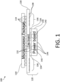
- FIG. 1 shows a module 100 that includes a microprocessor package 110 and a voltage regulator 120 joined to microprocessor package 110.
- Microprocessor package 110 includes at least a processor die and contacts.
- the microprocessor package can contain any type of processor, such as, for example, central processing unit (“CPU”), graphics processing unit (“GPU”), tensor processing unit (“TPU”), or any other type of processing unit which may generically be referred to as an "xPU.”
- Microprocessor package 110 could be an application specific integrated circuit (“ASIC").
- ASIC application specific integrated circuit
- the microprocessor package may optionally be an ASIC, and other arrangements are contemplated wherein an ASIC not containing a microprocessor could be used instead of the microprocessor package.
- Module 100 also includes contact pads 114 that each have a first side that contacts microprocessor package 110 and a second side that contacts voltage regulator 130.
- Contact pads 114 may each be monolithic.
- Contact pads 114 may be any electrically conductive elements suitable for connecting microprocessor package 110 and voltage regulator 120 together, such as, for example, pillars, solder balls, such as in a ball grid array, or fasteners.
- contact pads 114 may provide electrical connections between microprocessor package 110 and voltage regulator 120 in addition to mechanically joining microprocessor package 110 to voltage regulator 120.
- module 100 may include wires or other features for establishing electrical connection between microprocessor package 110 and voltage regulator 120.
- voltage regulator 120 to microprocessor package 110 by contact pads 114 as shown in the illustrated example avoids the delay and loss of power supplied to microprocessor package 110 by voltage regulator 120 that can occur in systems wherein a voltage regulator is separated from a microprocessor package by a PCBA or other substrates across which the power supply must travel.
- Voltage regulator 120 has a vertical power configuration and includes a capacitor board 130, a power board 140, and conductive pillars 134 connecting and establishing electrical contact between capacitor board 130 and power board 140.
- Capacitor board 130 may be a high density interconnect ("HDI") capacitor board.
- Conductive pillars 134 could be, for example, copper pillars, solder, a ball grid array, or any other electrically conductive elements suitable for connecting two boards together.
- Power board 140 may include inductors 142 that extend through a thickness of power board 140 as shown in the illustrated example.
- Voltage regulator 120 also includes transistors 144, such as, for example, field effect transistors or metal-oxide-semiconductor field effect transistors, on an underside of power board 140 that faces away from capacitor board 130. Voltage regulator 120 according to the illustrated example further includes capacitors 136 on an underside of capacitor board 130 that faces toward power board 140.
- transistors 144 such as, for example, field effect transistors or metal-oxide-semiconductor field effect transistors
- Voltage regulator 120 further includes capacitors 136 on an underside of capacitor board 130 that faces toward power board 140.
- the foregoing elements of voltage regulator 120 could be rearranged and some such elements could be omitted.
- inductors 142 in other arrangements may extend through only part of the thickness of power board 140
- capacitors 132 in other arrangements may be located elsewhere on or in capacitor board 130
- transistors 144 in other arrangements may be located elsewhere on or in power board 140.
- Module 100 also includes an electronic communication interface 136 for enabling electronic communication between module 100 and printed circuit board assemblies ("PCBAs") such as motherboards or other devices in which module 100 may be installed.
- Electronic communication interface 136 may be, for example, a land grid array (“LGA”), a pin grid array (“PGA”), or any other type of interface capable of creating an electronic connection across which data may be communicated.
- LGA land grid array
- PGA pin grid array
- communication interface 136 is located on the underside of capacitor board 130, facing away from microprocessor package 110 and toward power board 140 and surrounding power board 140 in a rectangular shape. In various other examples, communication interface 136 could be located on side surfaces or a top surface of capacitor board 130 or on any surface of power board 140.
- communication interface 136 could be located on any surface of microprocessor package 110 instead of or in addition to being located on an element of voltage regulator 120.
- module 110 could include multiple electronic communication interfaces 136 of the same type or of multiple different types.
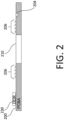
- FIG. 2 shows a printed circuit board assembly ("PCBA") 200, such as, for example, a motherboard, or any other type of PCBA, configured for use with module 100.
- PCBA 210 includes an aperture 210 into which at least part of module 100 may be inserted.
- One aperture 210 is shown, but PCBA 200 may include any number of apertures 210.
- aperture 210 is an opening that extends through and entire thickness of PCBA 200, but in other examples aperture 210 may extend through less than the entire thickness of PCBA 200.
- PCBA 200 according to the illustrated example includes an internally threaded bolt hole 204 to facilitate fastening module 100 to PCBA 200, but internally threaded bolt hole 204 may be omitted in other arrangements.
- PCBA 200 also includes electronic communication interface 206 extending around aperture 210 in a rectangular shape and matched to communication interface 136 of module 100.
- Communication interface 206 defines a flat socket on the top surface of PCBA 200 for operative engagement with module 100.
- communication interface 206 of PCBA 200 is a group of pins or other contacts configured for contacting the lands of the LGA
- communication interface 206 of PCBA 200 may be a group of contacts configured for receiving the pins of the PGA.
- modules 100 other than the illustrated example may have communication interfaces 136 in other locations and quantities and of various types
- PCBAs 200 other than the illustrated example may have communication interfaces 136 in locations, quantities, and types as necessary to engage with some or all of the communication interfaces 136 of any variation of module 100.
- Memory 230 may be, for example, random access memory ("RAM"), and in more specific examples double data rate RAM of any generation.
- RAM random access memory
- a single memory 230 is shown mounted to PCBA 200 for illustrative purposes, but multiple memory components may be mounted to PCBA 200, and other types of computer hardware may be mounted to PCBA 200 instead of or in addition to memory 230.
- FIG. 3 shows an assembly 240 created by inserting module 100 into aperture 210 such that the communication interfaces 136, 206 are engaged to one another to create a data connection 208 between module 100 and PCBA 200.
- Data connection 208 enables electronic communication between microprocessor package 110 and other components mounted to PCBA 200, such as memory 230.
- aperture 210 extends through the entire thickness of PCBA 200 as shown in the illustrated example, the underside of power board 140 is accessible from below PCBA 200. Connections to a power source can therefore be made directly to the underside of voltage regulator 120, meaning module 100 and PCBA 200 can be used with power supply arrangements similar to those used with other vertical power arrangements. In other implementations, including implementations where aperture 210 does not extend through the entire thickness of PCBA 200, power connections may extend through PCBA 200 into aperture 210 to supply power to voltage regulator 120 when module 100 is installed in aperture 210.
- module 100 is fastened to PCBA 200 by a bolt 220 disposed through a bolt hole 133 through capacitor board 130 and threadedly engaged with bolt hole 204 in PCBA 200, though in other examples bolt 220 and bolt holes 133, 204 may be omitted.
- Bolt hole 133 in capacitor board 130 is alignable with bolt hole 204 in PCBA 200 when module 100 is installed in aperture 210 to enable bolt 220 to extend through both bolt holes 133, 204.
- a conductive line 135 extends from bolt hole 204 of capacitor board 130 to at least one of the pillars 134 so that power can be supplied to or from power board 140 through bolt 220 via electrical contacts provided in bolt hole 204.
- power line 135 may be omitted in other examples.
- capacitor board 130 is laterally wider than aperture 210 on at least one axis that is horizontal from the perspective of FIG. 3 , and in some examples capacitor board 130 is wider than aperture 210 on two perpendicular axes that are horizontal from the perspective of FIG. 3 .
- Capacitor board 130 can therefore support module 100 on top of PCBA 200 while power board 140 is received in aperture 210.
- power board 140 is received in aperture 210 while capacitor board 130 and microprocessor package 110 remain outside of aperture 210.
- module 100 and PCBA 200 may be configured such that, when module 100 is installed in aperture 210 with communication interfaces 136, 206 in engagement, aperture 210 may receive part or all of capacitor board 130 instead of or in addition to power board 140, the entire voltage regulator 120 may be received in aperture 210, or part or all of microprocessor package 110 may be received in aperture 210 instead of or in addition to some or all of voltage regulator 120. In any case, module 100 may be plugged into aperture 210.
- module 100 and PCBA 200 avoids some of the warpage that can result from bonding a microprocessor package and a voltage regulator to opposite sides of a board in a clamshell arrangement.
- the freedom to plug and unplug module 100 in aperture 210 also avoids the solder reflow steps usually involved in bonding microprocessor packages and voltage regulators to boards with solder.
- PCBAs 200 designed for use with pluggable modules 100 can also remain in use as modules 100 fail or otherwise need to be replaced, since old modules 100 can simply be removed without the need to melt or break solder or other bonds between PCBA 200 and components of module 200.
- modules 100 can be easily reused in different PCBAs 200. Multiple modules 100, PCBAs 200, or both may be kept on hand to facilitate ease of replacement for either part.
- modules 100 and PCBAs 200 can simplify and reduce the cost of designing hardware for new applications.
- application specific integrated circuits can be created by creating a custom PCBA 200 designed for a particular need and plugging in modules 100 suitable for use in other applications.
- unique modules 100 could be designed to meet the needs of a specific application and plugged into a PCBA 200 suitable for use in other applications.
- FIG. 4 shows an assembly 440 according to another example.
- Assembly 440 includes a module 300 and a PCBA 400.
- modules shown in FIG. 4 in the 300 and 400 series are alike to like numbered elements in the 100 and 200 series, respectively, shown in FIGS. 1-3 except for specifically illustrated or stated differences.
- module 300, microprocessor package 310, and voltage regulator 320 are generally similar to module 100, microprocessor package 110, and voltage regulator 120, while PCBA 400 and aperture 410 are generally similar to PCBA 200 and aperture 210.
- Module 300 differs from module 100 in that capacitor board 330 is horizontally narrow enough to be received in aperture 410 so that the entirety of voltage regulator 320, which includes both power board 340 and capacitor board 330, can be inserted into aperture 410 as shown in FIG. 4 .
- Electronic communication interfaces 336 for module 300 are located on an underside of microprocessor package 310 to engage electronic communication interfaces 406 on top of PCBA 400 when module 300 is installed in aperture 410. Installing module 300 in aperture 410 can therefore create a data connection 408 between microprocessor package 310 and other components on PCBA 400, such as memory 430.
- a power supply connection 420 may be provided at or near an edge of aperture 410 to supply power to voltage regulator 320 through communication interfaces 336, 406 and microprocessor package 310. Though not illustrated in FIGS. 2 or 3 , a similar power supply connection could be provided at an edge of aperture 210 of PCBA 200 instead of or in addition to the power supply through bolt 220.
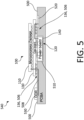
- FIG. 5 shows an assembly 540 according to another example.
- Assembly 540 includes module 100 and a PCBA 500.
- Features shown in FIG. 5 in the 500 series are alike to like numbered elements in the 200 series shown in FIGS. 1-3 except for specifically illustrated or stated differences. Accordingly, PCBA 500 and aperture 510 are generally similar to PCBA 200 and aperture 210.
- PCBA 500 differs from PCBA 200 in that aperture 210 does not extend through an entire thickness of PCBA 500.
- PCBA 500 is otherwise generally similar to PCBA 200, including electronic communication interface 506 adjacent aperture 510 for providing a data connection 508 between microprocessor package 110 and other components installed on PCBA 500, such as memory 530.
- PCBA 500 according to the illustrated example includes a power supply connection 520 at or near an edge of aperture 510 for providing power to voltage regulator 120 through interfaces 136, 506.
- PCBA 500 could be provided with a bolt hole and bolt similar to bolt hole 204 and bolt 220 to power voltage regulator 120 instead of or in addition to power supply connection 520.
Landscapes
- Engineering & Computer Science (AREA)
- Microelectronics & Electronic Packaging (AREA)
- Physics & Mathematics (AREA)
- Electromagnetism (AREA)
- Manufacturing & Machinery (AREA)
- Combinations Of Printed Boards (AREA)
- Power Sources (AREA)
Abstract
Description
- Vertical power arrangements meet the growing power demands of modern processors by mitigating power loss and delay. Typical vertical power arrangements include a voltage regulator bonded to an underside of a board directly under a powered component, such as a processor, on the top side of the board. The location of the voltage regulator directly on the opposite side of the board from the powered component enables a shorter power delivery path than some other arrangements where the voltage regulator is located on the same side of the board as the powered component. Power loss and delay tend to improve as the power delivery path gets shorter.
- These arrangements typically require two separate reflow steps to connect the voltage regulator and the component to the board. Changing or reconfiguring the voltage regulator or component may then require heating the board again, which may have unintended effects on elements that do not need to be reconfigured. Installing voltage regulators and processors this way can also result in warpage of the board, particularly where multiple pairs of voltage regulators and processors are installed on the same board.
- Vertical power arrangements can be improved by further shortening the power delivery path, reducing the difficulty of installing and replacing components, or both. Aspects of this disclosure are directed to a module that contains a microprocessor package, such as a central processing unit ("CPU") package, and a voltage regulator in a self-contained vertical power arrangement. The microprocessor package may be bonded or otherwise electrically connected directly to the voltage regulator, thereby minimizing the power delivery path.
- Further aspects of this disclosure are directed to a motherboard or other printed circuit board assembly ("PCBA") adapted for use with the module. The PCBA may include an aperture configured to receive the module and to enable simple connection of a power supply to the module when the module is installed in the aperture. The elements of the module may also be configured to support the module stably in the aperture. The PCBA may include an electronic communication interface in or near the aperture, and the module may include a corresponding interface configured for engaging with the PCBA's interface when the module is installed in the aperture. Thus, the module may be easily installed in and removed from the PCBA, meaning the module and the PCBA can each be replaced or reconfigured independently from the other. PCBAs may be provided with multiple apertures for multiple modules, and individual modules may be replaced without affecting the others. Multiple modules and multiple PCBAs may be kept on hand to replace failed parts as necessary. Modules may be customized as necessary for specific applications, then used with non-customized PCBAs. In other applications, PCBAs may be customized and used with non-customized modules.
- In another aspect, A pluggable processor module may comprise a central processing unit ("CPU") package, a voltage regulator including a capacitor board, and a contact pad that includes a first side in contact with the microprocessor package and a second side in contact with the capacitor board.
- In some arrangements according to any of the foregoing, the contact pad may be monolithic.
- In some arrangements according to any of the foregoing, the capacitor board may be wider than the microprocessor package.
- In some arrangements according to any of the foregoing, the capacitor board may include an electronic communication interface on a side that faces away from the microprocessor package.
- In some arrangements according to any of the foregoing, the voltage regulator may comprise a power board and conductive pillars electrically connecting the capacitor board to the power board.
- In some arrangements according to any of the foregoing, the capacitor board may include a bolt hole and a conductive line extending from the bolt hole to one of the conductive pillars.
- In some arrangements according to any of the foregoing, the voltage regulator may include inductors extending through the power board and transistors on a side of the power board facing away from the capacitor board.
- In another aspect, an assembly may comprise a pluggable processor module. The pluggable processor module may comprise a microprocessor package, a voltage regulator including a capacitor board, a power board, and conductive pillars connecting the capacitor board to the power board, and a contact pad that includes a first side in contact with the microprocessor package and a second side in contact with the capacitor board. The assembly may also comprise a PCBA that may include a module aperture that is large enough to receive the power board and narrower than the capacitor board.
- In some arrangements according to any of the foregoing, the PCBA may include a first electronic communication interface and the voltage regulator includes a second electronic communication interface configured to align with the first electronic communication interface when the power board is received in the module aperture.
- In some arrangements according to any of the foregoing, the first electronic communication interface may be adjacent to the module aperture and the second electronic communication interface may be on a side of the capacitor board that faces away from the microprocessor package.
- In some arrangements according to any of the foregoing, the second electronic communication interface may be a land grid array or a pin grid array.
- In some arrangements according to any of the foregoing, the PCBA may include a memory aperture in electronic communication with the first electronic communication interface.
- In some arrangements according to any of the foregoing, the PCBA may be configured to supply power to the first electronic communication interface.
- In some arrangements according to any of the foregoing, the PCBA may include a first bolt hole and the capacitor board includes a second bolt hole located to be alignable with the first bolt hole when the power board is received in the module aperture.
- In some arrangements according to any of the foregoing, the PCBA may be configured to supply voltage to the first bolt hole and the capacitor board may include a conductive line extending from the second bolt hole to one of the conductive pillars.
- In some arrangements according to any of the foregoing, the capacitor board may be wider than the microprocessor package.
- In some arrangements according to any of the foregoing, the module may be among a plurality of pluggable processor modules each including a microprocessor package and a voltage regulator that includes a power board receivable in the module aperture.
- In some arrangements according to any of the foregoing, wherein the module aperture may be a first module aperture and the PCBA may include a second module aperture that is large enough to receive the power board and narrower than the capacitor board.
- In some arrangements according to any of the foregoing, the module aperture may be a hole extending through the PCBA from a first side of the PCBA to a second side of the PCBA.
- In another aspect, a method may comprise plugging a pluggable processor module into a module aperture of a PCBA. The pluggable processor module may comprise a microprocessor package, a voltage regulator including a capacitor board, a power board, and conductive pillars connecting the capacitor board to the power board, and a contact pad that includes a first side in contact with the microprocessor package and a second side in contact with the capacitor board. The method may also comprise plugging the pluggable processor module into the module aperture may include inserting a portion of the voltage regulator into the module aperture and placing an electronic communication interface of the PCBA in contact with an electronic communication interface of the pluggable processor module.
-
-
FIG. 1 is a side elevation view of a pluggable module. -
FIG. 2 is a cross-sectional view of a printed circuit board assembly ("PCBA") adapted for use with the module ofFIG. 1 . -
FIG. 3 is a partial cross-sectional view of an assembly of the pluggable module ofFIG. 1 and the PCBA ofFIG. 2 . -
FIG. 4 is a partial cross-sectional view of an assembly of a pluggable module and a PCBA according to another aspect of the present disclosure. -
FIG. 5 is a partial cross-sectional view of an assembly of the pluggable module ofFIG. 1 and a PCBA according to another aspect of the present disclosure. - All directional terms, such as "up," "down," "above," "below," "vertical," or "height" used in the following description refer only to the orientation of features as depicted in the figure being described. Such directional terms are not intended to suggest that any features of the devices described herein must exist in any particular orientation when constructed.
-
FIG. 1 shows amodule 100 that includes amicroprocessor package 110 and avoltage regulator 120 joined tomicroprocessor package 110.Microprocessor package 110 includes at least a processor die and contacts. The microprocessor package can contain any type of processor, such as, for example, central processing unit ("CPU"), graphics processing unit ("GPU"), tensor processing unit ("TPU"), or any other type of processing unit which may generically be referred to as an "xPU."Microprocessor package 110 could be an application specific integrated circuit ("ASIC"). With respect to every reference to a microprocessor package in the present disclosure, the microprocessor package may optionally be an ASIC, and other arrangements are contemplated wherein an ASIC not containing a microprocessor could be used instead of the microprocessor package. -
Module 100 also includescontact pads 114 that each have a first side that contactsmicroprocessor package 110 and a second side that contactsvoltage regulator 130. Contactpads 114 may each be monolithic.Contact pads 114 may be any electrically conductive elements suitable for connectingmicroprocessor package 110 andvoltage regulator 120 together, such as, for example, pillars, solder balls, such as in a ball grid array, or fasteners. In implementations whereincontact pads 114 are electrically conductive,contact pads 114 may provide electrical connections betweenmicroprocessor package 110 andvoltage regulator 120 in addition to mechanically joiningmicroprocessor package 110 tovoltage regulator 120. In other examples,module 100 may include wires or other features for establishing electrical connection betweenmicroprocessor package 110 andvoltage regulator 120. The direct connection ofvoltage regulator 120 tomicroprocessor package 110 bycontact pads 114 as shown in the illustrated example avoids the delay and loss of power supplied tomicroprocessor package 110 byvoltage regulator 120 that can occur in systems wherein a voltage regulator is separated from a microprocessor package by a PCBA or other substrates across which the power supply must travel. -
Voltage regulator 120 according to the illustrated example has a vertical power configuration and includes acapacitor board 130, apower board 140, andconductive pillars 134 connecting and establishing electrical contact betweencapacitor board 130 andpower board 140.Capacitor board 130 may be a high density interconnect ("HDI") capacitor board.Conductive pillars 134 could be, for example, copper pillars, solder, a ball grid array, or any other electrically conductive elements suitable for connecting two boards together.Power board 140 may includeinductors 142 that extend through a thickness ofpower board 140 as shown in the illustrated example.Voltage regulator 120 according to the illustrated example also includestransistors 144, such as, for example, field effect transistors or metal-oxide-semiconductor field effect transistors, on an underside ofpower board 140 that faces away fromcapacitor board 130.Voltage regulator 120 according to the illustrated example further includescapacitors 136 on an underside ofcapacitor board 130 that faces towardpower board 140. In other examples, the foregoing elements ofvoltage regulator 120 could be rearranged and some such elements could be omitted. For example,inductors 142 in other arrangements may extend through only part of the thickness ofpower board 140,capacitors 132 in other arrangements may be located elsewhere on or incapacitor board 130, andtransistors 144 in other arrangements may be located elsewhere on or inpower board 140. -
Module 100 also includes anelectronic communication interface 136 for enabling electronic communication betweenmodule 100 and printed circuit board assemblies ("PCBAs") such as motherboards or other devices in whichmodule 100 may be installed.Electronic communication interface 136 may be, for example, a land grid array ("LGA"), a pin grid array ("PGA"), or any other type of interface capable of creating an electronic connection across which data may be communicated. In the illustrated example,communication interface 136 is located on the underside ofcapacitor board 130, facing away frommicroprocessor package 110 and towardpower board 140 and surroundingpower board 140 in a rectangular shape. In various other examples,communication interface 136 could be located on side surfaces or a top surface ofcapacitor board 130 or on any surface ofpower board 140. In further examples,communication interface 136 could be located on any surface ofmicroprocessor package 110 instead of or in addition to being located on an element ofvoltage regulator 120. In variations on any of the foregoing,module 110 could include multipleelectronic communication interfaces 136 of the same type or of multiple different types. -
FIG. 2 shows a printed circuit board assembly ("PCBA") 200, such as, for example, a motherboard, or any other type of PCBA, configured for use withmodule 100.PCBA 210 includes anaperture 210 into which at least part ofmodule 100 may be inserted. Oneaperture 210 is shown, butPCBA 200 may include any number ofapertures 210. In the illustrated example,aperture 210 is an opening that extends through and entire thickness ofPCBA 200, but inother examples aperture 210 may extend through less than the entire thickness ofPCBA 200.PCBA 200 according to the illustrated example includes an internally threadedbolt hole 204 to facilitatefastening module 100 toPCBA 200, but internally threadedbolt hole 204 may be omitted in other arrangements. -
PCBA 200 also includeselectronic communication interface 206 extending aroundaperture 210 in a rectangular shape and matched tocommunication interface 136 ofmodule 100.Communication interface 206 defines a flat socket on the top surface ofPCBA 200 for operative engagement withmodule 100. For example, in implementations wherecommunication interface 136 ofmodule 100 is an LGA,communication interface 206 ofPCBA 200 is a group of pins or other contacts configured for contacting the lands of the LGA, and in other implementations wherecommunication interface 136 of module is a PGA,communication interface 206 ofPCBA 200 may be a group of contacts configured for receiving the pins of the PGA. In the same manner thatmodules 100 other than the illustrated example may havecommunication interfaces 136 in other locations and quantities and of various types,PCBAs 200 other than the illustrated example may havecommunication interfaces 136 in locations, quantities, and types as necessary to engage with some or all of the communication interfaces 136 of any variation ofmodule 100. - Various other components may be mounted to
PCBA 200, such as, for example,memory 230.Memory 230 may be, for example, random access memory ("RAM"), and in more specific examples double data rate RAM of any generation. Asingle memory 230 is shown mounted toPCBA 200 for illustrative purposes, but multiple memory components may be mounted toPCBA 200, and other types of computer hardware may be mounted toPCBA 200 instead of or in addition tomemory 230. -
FIG. 3 shows anassembly 240 created by insertingmodule 100 intoaperture 210 such that the communication interfaces 136, 206 are engaged to one another to create a data connection 208 betweenmodule 100 andPCBA 200. Data connection 208 enables electronic communication betweenmicroprocessor package 110 and other components mounted toPCBA 200, such asmemory 230. - Where
aperture 210 extends through the entire thickness ofPCBA 200 as shown in the illustrated example, the underside ofpower board 140 is accessible from belowPCBA 200. Connections to a power source can therefore be made directly to the underside ofvoltage regulator 120, meaningmodule 100 andPCBA 200 can be used with power supply arrangements similar to those used with other vertical power arrangements. In other implementations, including implementations whereaperture 210 does not extend through the entire thickness ofPCBA 200, power connections may extend throughPCBA 200 intoaperture 210 to supply power tovoltage regulator 120 whenmodule 100 is installed inaperture 210. - In the illustrated example of
assembly 240,module 100 is fastened toPCBA 200 by abolt 220 disposed through abolt hole 133 throughcapacitor board 130 and threadedly engaged withbolt hole 204 inPCBA 200, though in other examples bolt 220 and boltholes Bolt hole 133 incapacitor board 130 is alignable withbolt hole 204 inPCBA 200 whenmodule 100 is installed inaperture 210 to enablebolt 220 to extend through both bolt holes 133, 204. In the illustrated example, aconductive line 135 extends frombolt hole 204 ofcapacitor board 130 to at least one of thepillars 134 so that power can be supplied to or frompower board 140 throughbolt 220 via electrical contacts provided inbolt hole 204. However,power line 135 may be omitted in other examples. - In
assembly 240,power board 140 is received inaperture 210 whilecapacitor board 130 andmicroprocessor package 110 sit atopPCBA 200.Capacitor board 130 is laterally wider thanaperture 210 on at least one axis that is horizontal from the perspective ofFIG. 3 , and in someexamples capacitor board 130 is wider thanaperture 210 on two perpendicular axes that are horizontal from the perspective ofFIG. 3 .Capacitor board 130 can therefore supportmodule 100 on top ofPCBA 200 whilepower board 140 is received inaperture 210. Thus, whenmodule 100 is installed inaperture 210 withcommunication interfaces power board 140 is received inaperture 210 whilecapacitor board 130 andmicroprocessor package 110 remain outside ofaperture 210. In various other configurations,module 100 andPCBA 200 may be configured such that, whenmodule 100 is installed inaperture 210 withcommunication interfaces aperture 210 may receive part or all ofcapacitor board 130 instead of or in addition topower board 140, theentire voltage regulator 120 may be received inaperture 210, or part or all ofmicroprocessor package 110 may be received inaperture 210 instead of or in addition to some or all ofvoltage regulator 120. In any case,module 100 may be plugged intoaperture 210. - The cooperative pluggable design of
module 100 andPCBA 200 avoids some of the warpage that can result from bonding a microprocessor package and a voltage regulator to opposite sides of a board in a clamshell arrangement. The freedom to plug and unplugmodule 100 inaperture 210 also avoids the solder reflow steps usually involved in bonding microprocessor packages and voltage regulators to boards with solder. -
PCBAs 200 designed for use withpluggable modules 100 can also remain in use asmodules 100 fail or otherwise need to be replaced, sinceold modules 100 can simply be removed without the need to melt or break solder or other bonds betweenPCBA 200 and components ofmodule 200. In other examples,modules 100 can be easily reused indifferent PCBAs 200.Multiple modules 100,PCBAs 200, or both may be kept on hand to facilitate ease of replacement for either part. - The interchangeability of
modules 100 and PCBAs 200 can simplify and reduce the cost of designing hardware for new applications. For example, application specific integrated circuits can be created by creating acustom PCBA 200 designed for a particular need and plugging inmodules 100 suitable for use in other applications. In other examples,unique modules 100 could be designed to meet the needs of a specific application and plugged into aPCBA 200 suitable for use in other applications. -
FIG. 4 shows anassembly 440 according to another example.Assembly 440 includes amodule 300 and aPCBA 400. Features shown inFIG. 4 in the 300 and 400 series are alike to like numbered elements in the 100 and 200 series, respectively, shown inFIGS. 1-3 except for specifically illustrated or stated differences. Accordingly,module 300,microprocessor package 310, andvoltage regulator 320 are generally similar tomodule 100,microprocessor package 110, andvoltage regulator 120, whilePCBA 400 andaperture 410 are generally similar toPCBA 200 andaperture 210. -
Module 300 differs frommodule 100 in thatcapacitor board 330 is horizontally narrow enough to be received inaperture 410 so that the entirety ofvoltage regulator 320, which includes bothpower board 340 andcapacitor board 330, can be inserted intoaperture 410 as shown inFIG. 4 . Electronic communication interfaces 336 formodule 300 are located on an underside ofmicroprocessor package 310 to engage electronic communication interfaces 406 on top ofPCBA 400 whenmodule 300 is installed inaperture 410. Installingmodule 300 inaperture 410 can therefore create adata connection 408 betweenmicroprocessor package 310 and other components onPCBA 400, such asmemory 430. Apower supply connection 420 may be provided at or near an edge ofaperture 410 to supply power tovoltage regulator 320 through communication interfaces 336, 406 andmicroprocessor package 310. Though not illustrated inFIGS. 2 or3 , a similar power supply connection could be provided at an edge ofaperture 210 ofPCBA 200 instead of or in addition to the power supply throughbolt 220. -
FIG. 5 shows anassembly 540 according to another example.Assembly 540 includesmodule 100 and aPCBA 500. Features shown inFIG. 5 in the 500 series are alike to like numbered elements in the 200 series shown inFIGS. 1-3 except for specifically illustrated or stated differences. Accordingly,PCBA 500 andaperture 510 are generally similar toPCBA 200 andaperture 210. -
PCBA 500 differs fromPCBA 200 in thataperture 210 does not extend through an entire thickness ofPCBA 500.PCBA 500 is otherwise generally similar toPCBA 200, including electronic communication interface 506adjacent aperture 510 for providing adata connection 508 betweenmicroprocessor package 110 and other components installed onPCBA 500, such asmemory 530.PCBA 500 according to the illustrated example includes apower supply connection 520 at or near an edge ofaperture 510 for providing power tovoltage regulator 120 throughinterfaces 136, 506. However, in other examples,PCBA 500 could be provided with a bolt hole and bolt similar to bolthole 204 and bolt 220 topower voltage regulator 120 instead of or in addition topower supply connection 520. - Although the concept herein has been described with reference to particular examples, it is to be understood that these examples are merely illustrative of the principles and applications of the present concept. It is therefore to be understood that numerous modifications may be made to the illustrative examples and that other arrangements may be devised without departing from the spirit and scope of the present concept as defined by the appended claims.
Claims (15)
- A pluggable processor module comprising:a microprocessor package;a voltage regulator including a capacitor board; anda contact pad that includes a first side in contact with the microprocessor package and a second side in contact with the capacitor board.
- The module of claim 1, the contact pad is monolithic.
- The module of claim 1 or claim 2, wherein the capacitor board is wider than the microprocessor package.
- The module of one of claims 1 to 3, wherein the capacitor board includes an electronic communication interface on a side that faces away from the microprocessor package.
- The module of one of claims 1 to 4, wherein the voltage regulator comprises a power board and conductive pillars electrically connecting the capacitor board to the power board.
- The module of claim 5, wherein the capacitor board includes a bolt hole and a conductive line extending from the bolt hole to one of the conductive pillars; and/or
wherein the voltage regulator includes inductors extending through the power board and transistors on a side of the power board facing away from the capacitor board. - An assembly comprising:
the pluggable processor module of one of claims 1 to 4 or 6; andwherein the pluggable processor module further comprises:
a power board, and conductive pillars connecting the capacitor board to the power board; andwherein the assembly further comprises:
a printed circuit board assembly ("PCBA") including a module aperture that is large enough to receive the power board and narrower than the capacitor board. - The assembly of claim 7, wherein the PCBA includes a first electronic communication interface and the voltage regulator includes a second electronic communication interface configured to align with the first electronic communication interface when the power board is received in the module aperture.
- The assembly of claim 8, wherein the first electronic communication interface is adjacent to the module aperture and the second electronic communication interface is on a side of the capacitor board that faces away from the microprocessor package.
- The assembly of claim 8 or claim 9, wherein the second electronic communication interface is a land grid array or a pin grid array.
- The assembly of one of claims 8 to 10, wherein the PCBA includes a memory aperture in electronic communication with the first electronic communication interface; and/or
wherein the PCBA is configured to supply power to the first electronic communication interface. - The assembly of one of claims 7 to 11, wherein the PCBA includes a first bolt hole and the capacitor board includes a second bolt hole located to be alignable with the first bolt hole when the power board is received in the module aperture.
- The assembly of claim 12, wherein the PCBA is configured to supply voltage to the first bolt hole and the capacitor board includes a conductive line extending from the second bolt hole to one of the conductive pillars.
- The assembly of one of claims 7 to 13, wherein the capacitor board is wider than the microprocessor package; and/orwherein the module is among a plurality of pluggable processor modules each including a microprocessor package and a voltage regulator that includes a power board receivable in the module aperture; and/orwherein the module aperture is a first module aperture and the PCBA includes a second module aperture that is large enough to receive the power board and narrower than the capacitor board; and/orwherein the module aperture is a hole extending through the PCBA from a first side of the PCBA to a second side of the PCBA.
- A method comprising plugging a pluggable processor module into a module aperture of a PCBA, wherein:
the pluggable processor module comprises:a microprocessor package;a voltage regulator including a capacitor board, a power board, and conductive pillars connecting the capacitor board to the power board; anda contact pad that includes a first side in contact with the microprocessor package and a second side in contact with the capacitor board; andplugging the pluggable processor module into the module aperture includes inserting a portion of the voltage regulator into the module aperture and placing an electronic communication interface of the PCBA in contact with an electronic communication interface of the pluggable processor module.
Applications Claiming Priority (1)
| Application Number | Priority Date | Filing Date | Title |
|---|---|---|---|
| US17/719,857 US12002795B2 (en) | 2022-04-13 | 2022-04-13 | Pluggable CPU modules with vertical power |
Publications (1)
| Publication Number | Publication Date |
|---|---|
| EP4262329A1 true EP4262329A1 (en) | 2023-10-18 |
Family
ID=84360390
Family Applications (1)
| Application Number | Title | Priority Date | Filing Date |
|---|---|---|---|
| EP22206401.6A Pending EP4262329A1 (en) | 2022-04-13 | 2022-11-09 | Pluggable cpu modules with vertical power |
Country Status (3)
| Country | Link |
|---|---|
| US (2) | US12002795B2 (en) |
| EP (1) | EP4262329A1 (en) |
| CN (1) | CN116027857A (en) |
Cited By (2)
| Publication number | Priority date | Publication date | Assignee | Title |
|---|---|---|---|---|
| WO2026041594A1 (en) * | 2024-08-21 | 2026-02-26 | Arm Limited | Vertical integrated voltage regulator |
| WO2026041595A1 (en) * | 2024-08-21 | 2026-02-26 | Arm Limited | Vertical integrated voltage regulator with circuit board cutout |
Families Citing this family (1)
| Publication number | Priority date | Publication date | Assignee | Title |
|---|---|---|---|---|
| JP7409143B2 (en) * | 2020-02-19 | 2024-01-09 | 株式会社オートネットワーク技術研究所 | connector |
Citations (2)
| Publication number | Priority date | Publication date | Assignee | Title |
|---|---|---|---|---|
| US5481436A (en) * | 1992-12-30 | 1996-01-02 | Interconnect Systems, Inc. | Multi-level assemblies and methods for interconnecting integrated circuits |
| US20080116589A1 (en) * | 2006-11-17 | 2008-05-22 | Zong-Fu Li | Ball grid array package assembly with integrated voltage regulator |
Family Cites Families (67)
| Publication number | Priority date | Publication date | Assignee | Title |
|---|---|---|---|---|
| US4631820A (en) | 1984-08-23 | 1986-12-30 | Canon Kabushiki Kaisha | Mounting assembly and mounting method for an electronic component |
| JPH047865A (en) | 1990-04-25 | 1992-01-13 | Hitachi Ltd | Lead frame and semiconductor integrated circuit device using the same |
| US5175613A (en) | 1991-01-18 | 1992-12-29 | Digital Equipment Corporation | Package for EMI, ESD, thermal, and mechanical shock protection of circuit chips |
| JP2931741B2 (en) | 1993-09-24 | 1999-08-09 | 株式会社東芝 | Semiconductor device |
| US5886408A (en) | 1994-09-08 | 1999-03-23 | Fujitsu Limited | Multi-chip semiconductor device |
| US5608262A (en) | 1995-02-24 | 1997-03-04 | Lucent Technologies Inc. | Packaging multi-chip modules without wire-bond interconnection |
| JPH08274214A (en) | 1995-03-30 | 1996-10-18 | Seiko Epson Corp | Semiconductor device |
| US5847929A (en) | 1996-06-28 | 1998-12-08 | International Business Machines Corporation | Attaching heat sinks directly to flip chips and ceramic chip carriers |
| KR100258350B1 (en) | 1997-05-13 | 2000-06-01 | 마이클 디. 오브라이언 | Super bga semiconductor package |
| JP3087709B2 (en) | 1997-12-08 | 2000-09-11 | 日本電気株式会社 | Semiconductor device and manufacturing method thereof |
| JP3482850B2 (en) | 1997-12-08 | 2004-01-06 | セイコーエプソン株式会社 | Semiconductor device and its manufacturing method, circuit board, and electronic equipment |
| DE19816794A1 (en) | 1998-04-16 | 1999-10-21 | Bosch Gmbh Robert | Printed circuit board system, for electronic combination instrument |
| WO2000004595A2 (en) | 1998-07-20 | 2000-01-27 | Intel Corporation | Land-side mounting of components to an integrated circuit package |
| US6154371A (en) | 1998-09-30 | 2000-11-28 | Cisco Technology, Inc. | Printed circuit board assembly and method |
| US20030156400A1 (en) | 1999-07-15 | 2003-08-21 | Dibene Joseph Ted | Method and apparatus for providing power to a microprocessor with intergrated thermal and EMI management |
| US6356448B1 (en) * | 1999-11-02 | 2002-03-12 | Inceptechnologies, Inc. | Inter-circuit encapsulated packaging for power delivery |
| US20030214800A1 (en) * | 1999-07-15 | 2003-11-20 | Dibene Joseph Ted | System and method for processor power delivery and thermal management |
| US6741480B2 (en) * | 1999-07-15 | 2004-05-25 | Incep Technologies, Inc. | Integrated power delivery with flex circuit interconnection for high density power circuits for integrated circuits and systems |
| JP3414342B2 (en) | 1999-11-25 | 2003-06-09 | 日本電気株式会社 | Mounting structure and mounting method of integrated circuit chip |
| EP1189282A4 (en) | 2000-03-21 | 2006-02-15 | Mitsubishi Electric Corp | SEMICONDUCTOR DEVICE, METHOD FOR PRODUCING ELECTRONIC DEVICE, ELECTRONIC DEVICE, AND PORTABLE INFORMATION TERMINAL |
| JP2001308258A (en) | 2000-04-26 | 2001-11-02 | Sony Corp | Semiconductor package and manufacturing method thereof |
| US7247932B1 (en) | 2000-05-19 | 2007-07-24 | Megica Corporation | Chip package with capacitor |
| JP4497683B2 (en) | 2000-09-11 | 2010-07-07 | ローム株式会社 | Integrated circuit device |
| US6760232B2 (en) * | 2001-03-16 | 2004-07-06 | Sun Microsystems, Inc. | Power distribution system having a dedicated power structure with apertures for mounting integrated circuit packages |
| JP2002314031A (en) | 2001-04-13 | 2002-10-25 | Fujitsu Ltd | Multi-chip module |
| US7222243B2 (en) * | 2001-04-26 | 2007-05-22 | Tyco Electronics Corporation | Power delivery system for a microprocessor |
| DE10142655A1 (en) | 2001-08-31 | 2003-04-03 | Epcos Ag | component assembly |
| US6611435B2 (en) * | 2002-01-08 | 2003-08-26 | Intel Corporation | voltage regulator with voltage droop compensation |
| US6837719B2 (en) * | 2002-02-25 | 2005-01-04 | Molex Incorporated | Connector with included filtered power delivery |
| JP3093800U (en) | 2002-11-01 | 2003-05-16 | アルプス電気株式会社 | Electronic unit |
| JP2004288834A (en) * | 2003-03-20 | 2004-10-14 | Fujitsu Ltd | Electronic component mounting method, mounting structure and package substrate |
| JPWO2004112450A1 (en) | 2003-06-12 | 2006-07-20 | 富士通株式会社 | Substrate mounting method and mounting structure |
| US7180165B2 (en) | 2003-09-05 | 2007-02-20 | Sanmina, Sci Corporation | Stackable electronic assembly |
| US20050127484A1 (en) | 2003-12-16 | 2005-06-16 | Texas Instruments Incorporated | Die extender for protecting an integrated circuit die on a flip chip package |
| DE202004002332U1 (en) | 2004-02-11 | 2004-04-22 | Siemens Ag | circuit board |
| US7257004B2 (en) * | 2004-05-06 | 2007-08-14 | Tyco Electronics Corporation | Power delivery system for integrated circuits |
| US7145782B2 (en) * | 2004-07-16 | 2006-12-05 | Intel Corporation | Reducing loadline impedance in a system |
| US7085143B1 (en) | 2005-05-23 | 2006-08-01 | International Business Machines Corporation | In-module current source |
| JP4585416B2 (en) | 2005-09-22 | 2010-11-24 | 富士通株式会社 | Substrate warpage reduction structure and substrate warpage reduction method |
| US7476978B2 (en) | 2006-05-17 | 2009-01-13 | Infineon Technologies, Ag | Electronic component having a semiconductor power device |
| US7886431B2 (en) | 2006-06-06 | 2011-02-15 | Teraspeed Consulting Group Llc | Power distribution system for integrated circuits |
| US7773390B2 (en) | 2006-06-06 | 2010-08-10 | Teraspeed Consulting Group Llc | Power distribution system for integrated circuits |
| US7646093B2 (en) * | 2006-12-20 | 2010-01-12 | Intel Corporation | Thermal management of dies on a secondary side of a package |
| JP4609435B2 (en) | 2007-01-30 | 2011-01-12 | パナソニック株式会社 | Component-embedded substrate, electronic device using the same, and manufacturing method used therefor |
| US20090028491A1 (en) * | 2007-07-26 | 2009-01-29 | General Electric Company | Interconnect structure |
| US8837159B1 (en) | 2009-10-28 | 2014-09-16 | Amazon Technologies, Inc. | Low-profile circuit board assembly |
| JPWO2011121779A1 (en) | 2010-03-31 | 2013-07-04 | 富士通株式会社 | MULTI-CHIP MODULE, PRINTED WIRING BOARD UNIT, MULTI-CHIP MODULE MANUFACTURING METHOD, AND PRINTED WIRING BOARD UNIT MANUFACTURING METHOD |
| US8513798B2 (en) | 2010-09-09 | 2013-08-20 | Infineon Technologies Ag | Power semiconductor chip package |
| US8426258B2 (en) | 2010-10-12 | 2013-04-23 | Io Semiconductor, Inc. | Vertical semiconductor device with thinned substrate |
| US8737080B2 (en) * | 2011-01-14 | 2014-05-27 | Qualcomm Incorporated | Modular surface mount package for a system on a chip |
| US10312361B2 (en) | 2011-06-20 | 2019-06-04 | The Regents Of The University Of California | Trenched vertical power field-effect transistors with improved on-resistance and breakdown voltage |
| EP2627160A1 (en) | 2012-02-08 | 2013-08-14 | Harman Becker Automotive Systems GmbH | Circuit board system |
| JP2014027020A (en) * | 2012-07-24 | 2014-02-06 | Toshiba Corp | Circuit board, electronic apparatus, and manufacturing method of circuit board |
| JP6253885B2 (en) | 2013-01-07 | 2017-12-27 | ルネサスエレクトロニクス株式会社 | Vertical power MOSFET |
| US11901274B2 (en) * | 2015-09-25 | 2024-02-13 | Intel Corporation | Packaged integrated circuit device with recess structure |
| WO2017111903A1 (en) * | 2015-12-21 | 2017-06-29 | Intel Corporation | Integrating system in package (sip) with input/output (io) board for platform miniaturization |
| WO2018182643A1 (en) | 2017-03-30 | 2018-10-04 | Intel Corporation | Three-dimensional decoupling integration within hole in motherboard |
| US10548249B2 (en) * | 2017-09-27 | 2020-01-28 | Intel Corporation | Shielding in electronic assemblies |
| EP3582259B1 (en) | 2018-06-11 | 2021-11-03 | AT & S Austria Technologie & Systemtechnik Aktiengesellschaft | Stepped component assembly accommodated within a stepped cavity in component carrier |
| CN109618538B (en) | 2018-12-29 | 2020-10-27 | 联想(北京)有限公司 | Accommodation equipment |
| US10827616B2 (en) * | 2019-01-30 | 2020-11-03 | Kyocera Corporation | Mounting structure |
| US20200373260A1 (en) * | 2019-05-24 | 2020-11-26 | Microsoft Technology Licensing, Llc | Decoupling capacitance arrangements for integrated circuit devices |
| US11452246B2 (en) * | 2020-03-25 | 2022-09-20 | Qualcomm Incorporated | Patch substrate configured as a shield located over a cavity of a board |
| US11343906B2 (en) * | 2020-06-08 | 2022-05-24 | Intel Corporation | Stacked scalable voltage regulator module for platform area miniaturization |
| US12224252B2 (en) * | 2020-09-23 | 2025-02-11 | Intel Corporation | Magnetic core inductors in interposer |
| US12328816B2 (en) * | 2021-08-25 | 2025-06-10 | Intel Corporation | Asymmetrical laminated circuit boards for improved electrical performance |
| US12308543B2 (en) * | 2022-04-18 | 2025-05-20 | Google Llc | Structure for optimal XPU socket compression |
-
2022
- 2022-04-13 US US17/719,857 patent/US12002795B2/en active Active
- 2022-11-09 EP EP22206401.6A patent/EP4262329A1/en active Pending
-
2023
- 2023-01-10 CN CN202310037049.3A patent/CN116027857A/en active Pending
-
2024
- 2024-05-09 US US18/659,676 patent/US12469830B2/en active Active
Patent Citations (2)
| Publication number | Priority date | Publication date | Assignee | Title |
|---|---|---|---|---|
| US5481436A (en) * | 1992-12-30 | 1996-01-02 | Interconnect Systems, Inc. | Multi-level assemblies and methods for interconnecting integrated circuits |
| US20080116589A1 (en) * | 2006-11-17 | 2008-05-22 | Zong-Fu Li | Ball grid array package assembly with integrated voltage regulator |
Cited By (2)
| Publication number | Priority date | Publication date | Assignee | Title |
|---|---|---|---|---|
| WO2026041594A1 (en) * | 2024-08-21 | 2026-02-26 | Arm Limited | Vertical integrated voltage regulator |
| WO2026041595A1 (en) * | 2024-08-21 | 2026-02-26 | Arm Limited | Vertical integrated voltage regulator with circuit board cutout |
Also Published As
| Publication number | Publication date |
|---|---|
| US20240290763A1 (en) | 2024-08-29 |
| CN116027857A (en) | 2023-04-28 |
| US20230335541A1 (en) | 2023-10-19 |
| US12002795B2 (en) | 2024-06-04 |
| US12469830B2 (en) | 2025-11-11 |
Similar Documents
| Publication | Publication Date | Title |
|---|---|---|
| US12469830B2 (en) | Method of plugging a pluggable processor into a PCBA | |
| US8018738B2 (en) | Voltage regulator attach for high current chip applications | |
| US7245507B2 (en) | Method and apparatus for providing power to a microprocessor with integrated thermal and EMI management | |
| US6847529B2 (en) | Ultra-low impedance power interconnection system for electronic packages | |
| US7881072B2 (en) | System and method for processor power delivery and thermal management | |
| US20020172022A1 (en) | Method and apparatus for providing power to a microprocessor with integrated thermal and EMI management | |
| US6623279B2 (en) | Separable power delivery connector | |
| US7298628B2 (en) | Power delivery to base of processor | |
| US7411283B2 (en) | Interconnect design for reducing radiated emissions | |
| US6556455B2 (en) | Ultra-low impedance power interconnection system for electronic packages | |
| US8958214B2 (en) | Motherboard assembly for interconnecting and distributing signals and power | |
| US6979784B1 (en) | Component power interface board | |
| WO1998002954A1 (en) | Power pad/power delivery system | |
| US7257004B2 (en) | Power delivery system for integrated circuits | |
| US6540525B1 (en) | High I/O stacked modules for integrated circuits | |
| US5671121A (en) | Kangaroo multi-package interconnection concept | |
| WO2001065344A2 (en) | Method and apparatus for providing power to a microprocessor with integrated thermal and emi management | |
| US7778041B2 (en) | Interconnection system between CPU and voltage regulator | |
| US6741480B2 (en) | Integrated power delivery with flex circuit interconnection for high density power circuits for integrated circuits and systems | |
| HK40088766A (en) | Pluggable cpu modules with vertical power | |
| US20020151195A1 (en) | Power interconnect method utilizing a flexible circuit between a voltage regulation module and an integrated circuit substrate | |
| US20070257691A1 (en) | Electrical connector assembly |
Legal Events
| Date | Code | Title | Description |
|---|---|---|---|
| PUAI | Public reference made under article 153(3) epc to a published international application that has entered the european phase |
Free format text: ORIGINAL CODE: 0009012 |
|
| STAA | Information on the status of an ep patent application or granted ep patent |
Free format text: STATUS: THE APPLICATION HAS BEEN PUBLISHED |
|
| AK | Designated contracting states |
Kind code of ref document: A1 Designated state(s): AL AT BE BG CH CY CZ DE DK EE ES FI FR GB GR HR HU IE IS IT LI LT LU LV MC ME MK MT NL NO PL PT RO RS SE SI SK SM TR |
|
| STAA | Information on the status of an ep patent application or granted ep patent |
Free format text: STATUS: REQUEST FOR EXAMINATION WAS MADE |
|
| 17P | Request for examination filed |
Effective date: 20240417 |
|
| RBV | Designated contracting states (corrected) |
Designated state(s): AL AT BE BG CH CY CZ DE DK EE ES FI FR GB GR HR HU IE IS IT LI LT LU LV MC ME MK MT NL NO PL PT RO RS SE SI SK SM TR |
|
| STAA | Information on the status of an ep patent application or granted ep patent |
Free format text: STATUS: EXAMINATION IS IN PROGRESS |
|
| 17Q | First examination report despatched |
Effective date: 20251118 |