EP4262327A1 - Devices and methods to improve thermal conduction from smt and chip on board components to chassis heat sinking - Google Patents
Devices and methods to improve thermal conduction from smt and chip on board components to chassis heat sinking Download PDFInfo
- Publication number
- EP4262327A1 EP4262327A1 EP23167737.8A EP23167737A EP4262327A1 EP 4262327 A1 EP4262327 A1 EP 4262327A1 EP 23167737 A EP23167737 A EP 23167737A EP 4262327 A1 EP4262327 A1 EP 4262327A1
- Authority
- EP
- European Patent Office
- Prior art keywords
- thermally conductive
- electrically
- circuit board
- insert
- board assembly
- Prior art date
- Legal status (The legal status is an assumption and is not a legal conclusion. Google has not performed a legal analysis and makes no representation as to the accuracy of the status listed.)
- Pending
Links
Images


Classifications
-
- H—ELECTRICITY
- H05—ELECTRIC TECHNIQUES NOT OTHERWISE PROVIDED FOR
- H05K—PRINTED CIRCUITS; CASINGS OR CONSTRUCTIONAL DETAILS OF ELECTRIC APPARATUS; MANUFACTURE OF ASSEMBLAGES OF ELECTRICAL COMPONENTS
- H05K1/00—Printed circuits
- H05K1/02—Details
- H05K1/0201—Thermal arrangements, e.g. for cooling, heating or preventing overheating
- H05K1/0203—Cooling of mounted components
- H05K1/0207—Cooling of mounted components using internal conductor planes parallel to the surface for thermal conduction, e.g. power planes
-
- H—ELECTRICITY
- H05—ELECTRIC TECHNIQUES NOT OTHERWISE PROVIDED FOR
- H05K—PRINTED CIRCUITS; CASINGS OR CONSTRUCTIONAL DETAILS OF ELECTRIC APPARATUS; MANUFACTURE OF ASSEMBLAGES OF ELECTRICAL COMPONENTS
- H05K1/00—Printed circuits
- H05K1/02—Details
- H05K1/0201—Thermal arrangements, e.g. for cooling, heating or preventing overheating
- H05K1/0203—Cooling of mounted components
- H05K1/0204—Cooling of mounted components using means for thermal conduction connection in the thickness direction of the substrate
-
- H—ELECTRICITY
- H05—ELECTRIC TECHNIQUES NOT OTHERWISE PROVIDED FOR
- H05K—PRINTED CIRCUITS; CASINGS OR CONSTRUCTIONAL DETAILS OF ELECTRIC APPARATUS; MANUFACTURE OF ASSEMBLAGES OF ELECTRICAL COMPONENTS
- H05K1/00—Printed circuits
- H05K1/02—Details
- H05K1/0201—Thermal arrangements, e.g. for cooling, heating or preventing overheating
- H05K1/0203—Cooling of mounted components
- H05K1/021—Components thermally connected to metal substrates or heat-sinks by insert mounting
-
- H—ELECTRICITY
- H05—ELECTRIC TECHNIQUES NOT OTHERWISE PROVIDED FOR
- H05K—PRINTED CIRCUITS; CASINGS OR CONSTRUCTIONAL DETAILS OF ELECTRIC APPARATUS; MANUFACTURE OF ASSEMBLAGES OF ELECTRICAL COMPONENTS
- H05K1/00—Printed circuits
- H05K1/02—Details
- H05K1/0213—Electrical arrangements not otherwise provided for
- H05K1/0263—High current adaptations, e.g. printed high current conductors or using auxiliary non-printed means; Fine and coarse circuit patterns on one circuit board
- H05K1/0265—High current adaptations, e.g. printed high current conductors or using auxiliary non-printed means; Fine and coarse circuit patterns on one circuit board characterized by the lay-out of or details of the printed conductors, e.g. reinforced conductors, redundant conductors, conductors having different cross-sections
-
- H—ELECTRICITY
- H05—ELECTRIC TECHNIQUES NOT OTHERWISE PROVIDED FOR
- H05K—PRINTED CIRCUITS; CASINGS OR CONSTRUCTIONAL DETAILS OF ELECTRIC APPARATUS; MANUFACTURE OF ASSEMBLAGES OF ELECTRICAL COMPONENTS
- H05K1/00—Printed circuits
- H05K1/02—Details
- H05K1/09—Use of materials for the conductive, e.g. metallic pattern
-
- H—ELECTRICITY
- H05—ELECTRIC TECHNIQUES NOT OTHERWISE PROVIDED FOR
- H05K—PRINTED CIRCUITS; CASINGS OR CONSTRUCTIONAL DETAILS OF ELECTRIC APPARATUS; MANUFACTURE OF ASSEMBLAGES OF ELECTRICAL COMPONENTS
- H05K1/00—Printed circuits
- H05K1/18—Printed circuits structurally associated with non-printed electric components
- H05K1/181—Printed circuits structurally associated with non-printed electric components associated with surface mounted components
-
- H—ELECTRICITY
- H05—ELECTRIC TECHNIQUES NOT OTHERWISE PROVIDED FOR
- H05K—PRINTED CIRCUITS; CASINGS OR CONSTRUCTIONAL DETAILS OF ELECTRIC APPARATUS; MANUFACTURE OF ASSEMBLAGES OF ELECTRICAL COMPONENTS
- H05K3/00—Apparatus or processes for manufacturing printed circuits
- H05K3/10—Apparatus or processes for manufacturing printed circuits in which conductive material is applied to the insulating support in such a manner as to form the desired conductive pattern
- H05K3/107—Apparatus or processes for manufacturing printed circuits in which conductive material is applied to the insulating support in such a manner as to form the desired conductive pattern by filling grooves in the support with conductive material
-
- H—ELECTRICITY
- H05—ELECTRIC TECHNIQUES NOT OTHERWISE PROVIDED FOR
- H05K—PRINTED CIRCUITS; CASINGS OR CONSTRUCTIONAL DETAILS OF ELECTRIC APPARATUS; MANUFACTURE OF ASSEMBLAGES OF ELECTRICAL COMPONENTS
- H05K2201/00—Indexing scheme relating to printed circuits covered by H05K1/00
- H05K2201/03—Conductive materials
- H05K2201/0302—Properties and characteristics in general
-
- H—ELECTRICITY
- H05—ELECTRIC TECHNIQUES NOT OTHERWISE PROVIDED FOR
- H05K—PRINTED CIRCUITS; CASINGS OR CONSTRUCTIONAL DETAILS OF ELECTRIC APPARATUS; MANUFACTURE OF ASSEMBLAGES OF ELECTRICAL COMPONENTS
- H05K2201/00—Indexing scheme relating to printed circuits covered by H05K1/00
- H05K2201/03—Conductive materials
- H05K2201/032—Materials
-
- H—ELECTRICITY
- H05—ELECTRIC TECHNIQUES NOT OTHERWISE PROVIDED FOR
- H05K—PRINTED CIRCUITS; CASINGS OR CONSTRUCTIONAL DETAILS OF ELECTRIC APPARATUS; MANUFACTURE OF ASSEMBLAGES OF ELECTRICAL COMPONENTS
- H05K2201/00—Indexing scheme relating to printed circuits covered by H05K1/00
- H05K2201/10—Details of components or other objects attached to or integrated in a printed circuit board
- H05K2201/10007—Types of components
- H05K2201/10166—Transistor
-
- H—ELECTRICITY
- H05—ELECTRIC TECHNIQUES NOT OTHERWISE PROVIDED FOR
- H05K—PRINTED CIRCUITS; CASINGS OR CONSTRUCTIONAL DETAILS OF ELECTRIC APPARATUS; MANUFACTURE OF ASSEMBLAGES OF ELECTRICAL COMPONENTS
- H05K2201/00—Indexing scheme relating to printed circuits covered by H05K1/00
- H05K2201/10—Details of components or other objects attached to or integrated in a printed circuit board
- H05K2201/10227—Other objects, e.g. metallic pieces
- H05K2201/10416—Metallic blocks or heatsinks completely inserted in a PCB
-
- H—ELECTRICITY
- H05—ELECTRIC TECHNIQUES NOT OTHERWISE PROVIDED FOR
- H05K—PRINTED CIRCUITS; CASINGS OR CONSTRUCTIONAL DETAILS OF ELECTRIC APPARATUS; MANUFACTURE OF ASSEMBLAGES OF ELECTRICAL COMPONENTS
- H05K3/00—Apparatus or processes for manufacturing printed circuits
- H05K3/0058—Laminating printed circuit boards onto other substrates, e.g. metallic substrates
- H05K3/0061—Laminating printed circuit boards onto other substrates, e.g. metallic substrates onto a metallic substrate, e.g. a heat sink
Definitions
- circuit boards are often a major limiting design factor. In cases when such boards carry power semiconductors, thermal dissipation is even more critical. In many applications, circuit boards are carried by a chassis which functions as structural support, electrical ground and an important part of the pathway for thermal dissipation for one or more circuit boards.
- Advancing technologies permit fabrication of components with smaller physical sizes, which can then be placed onto boards closer together, while newer chip-on-board (“COB”) designs, have semiconductors and power semiconductors mounted to bare copper of a board.
- COB chip-on-board
- This newer process eliminates the semiconductor package, and as a result it is not possible to mount such components so that they are coupled directly to a heat sink, which presents a substantial obstacle to removing large amounts of heat from components directly through dedicated heat sinks.
- Older through-hole style devices can be mounted to vertical heat sinks with electrical leads passing through the PCB to make electrical contact, while the back side of the device package conducts heat to the vertical heat sink, which leverages more surface area to dissipate the heat into the surrounding air. Such a configuration is not feasible with dense COB designs.
- PCB assemblies use stacked up layers of copper and insulator material such as FR4, a fiberglass-epoxy composite.
- the copper conducts heat very well but when the heat has to be passed from one piece of copper to another to maintain voltage isolation the FR4 in between results in a very high thermal resistance-- on the order of 1000 times that of an equivalent shape of copper.
- a multilayer board was made from multiple 2 layer boards, each starting with laminated copper on both sides and then etched down to create isolated copper areas and traces as needed. This approach can only result with the original insulator material such as FR4 left between the copper layers since it started out completely laminated on both sides by copper.
- devices and methods are provided that enhance the thermal performance of circuit boards-particularly those in dense configurations and housed in a chassis or otherwise in contact with a heat sink.
- a circuit board assembly in accordance with one aspect of the present invention, includes a circuit board portion having a recess formed therein, an electrically and thermally conductive insert, shaped to fit in the recess formed in the circuit board portion, an electrically and thermally conductive layer adapted and configured to interface with an external chassis, and a thermally conductive electrically insulative portion interposed between the electrically and thermally conductive insert and the electrically and thermally conductive layer, adapted and configured to conduct heat from the electrically and thermally conductive insert to the electrically and thermally conductive layer without conducting electricity.
- the circuit board assembly can further include one or more semiconductor circuit elements mounted thereto, such as a MOSFET.
- the circuit board portion can be formed from a composite material, such as, but not limited to FR4.
- the circuit board portion can have one or more circuit traces formed thereon.
- the circuit traces can be provided in one or multiple layers.
- the thermally conductive electrically insulative portion can be a continuous region of material.
- the thermally conductive electrically insulative portion can include discontinuous regions of thermally conductive electrically insulative material dispersed within a layer of circuit board material, or other suitable material.
- Circuit board assemblies in accordance with the invention can further include a second electrically and thermally conductive insert, shaped to fit in a second recess formed in the circuit board portion. Similarly, third and subsequent inserts can be provided, as required.
- a method of forming a circuit board assembly includes forming a recess in a circuit board portion, forming an electrically and thermally conductive insert, shaped to fit in the recess of the circuit board portion, placing the insert in the recess, forming an electrically and thermally conductive layer adapted and configured to interface with an external chassis, forming a thermally conductive electrically insulative portion, interposing the thermally conductive electrically insulative portion between the electrically and thermally conductive insert and the electrically and thermally conductive layer, and bonding the layers together.
- the devices and related methods of the present invention benefit from aspects of newer construction techniques for thick copper boards where copper pieces are milled and inlayed into a PCB material.
- copper elements are assembled as separate pieces, instead of being etched down from copper clad laminate.
- Applicants have recognized, therefore, an opportunity to embed a high thermal conductivity electrical insulator material between thick copper layers and thereby to dramatically improve thermal conduction.
- devices in accordance with the invention benefit from effective thermal conduction from electrically live layers through thermal pads and into chassis ground layers, that in-turn can carry it off to a chassis and/or heat sink areas.
- Devices in accordance with the invention have the potential to reduce temperature drop between copper layers by many times, thus dramatically reducing the temperature of COB and other SMT parts. As a result, higher currents can be controlled in the same board area and higher density of components can be achieved, due to a need for less surface area to couple the heat into surrounding air.
- thermally conductive electrical insulator material between layers of copper.
- TCEI thermally conductive electrical insulator
- such material can be selected from materials typically used as thermally conductive, electrical isolative materials.
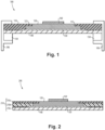
- FIG. 1 there is illustrated a cross-sectional view of a PCB assembly in accordance with a first embodiment of a circuit board assembly of the present invention, and which is designated generally by reference numeral 100.
- the PCB assembly 100 is illustrated being held in an external chassis 190 by wedgelocks 150.
- the PCB assembly includes a circuit board portion 110, which typically will have one or more circuit traces formed thereon, and may include multiple layers of composite circuit board material and electrical traces, although in the embodiment of Figure 1 , one layer is shown.
- a recess 115 is formed in the circuit board portion to hold a correspondingly shaped insert 120.
- the recess 115 may be formed in any suitable manner, including molding the shape at the time of manufacture of the material of the circuit board portion 110, or by a later machining or milling step, for example.
- the insert 120 is preferably electrically and thermally conductive to meet the requirements of applications of the assembly 100, and is preferably formed of solid metallic copper, although if desired, other materials can be used, including but not limited to silver, or aluminum, for example depending on the electrical, thermal and structural requirements of the particular implementation.
- the insert 120 can be provided with an upper face having a step 123 to engage with a complementary profile of the recess 115 of the circuit board portion 110. In this manner, the circuit board portion 110 fully captures the insert 120, thereby improving structural integrity of the overall assembly 100.
- the assembly 100 is illustrated with a semiconductor 160 mounted on the insert.
- the full configuration of the insert (or inserts) 120 will be as needed, determined by the function and configuration of the semiconductor 160.
- a power MOSFET will have at least two high-current carrying legs (source and drain), and a gate - each of which will require external connections, which can be accomplished by respective inserts 120.
- an electrically and thermally conductive base layer 140 is provided in the assembly 100, and is adapted and configured to interface with the external chassis 190 directly or by way of any ancillary fixing components such as the wedgelocks 150. It is this base 140 that conducts heat away from heat generating components (e.g. semiconductor 160) to the chassis for dissipation.
- the base extends at least from central areas of the board where heat is generated toward outer edges of the board where heat is dissipated to the chassis.
- the material for the base 140 is preferably highly thermally conductive, such as metallic copper, but other suitable materials can be used.
- thermally conductive electrically insulative portion 130 Interposed between the base 140 and the insert 120 is a thermally conductive electrically insulative portion 130, which can be a layer or a portion of a layer, depending on the mechanical characteristics of the material from which the thermally conductive electrically insulative portion 130 is formed. As illustrated in Figure 1 , the thermally conductive electrically insulative portion 130 preferably extends at least some distance beyond the extents of the insert 120 so as to provide a good voltage barrier between the electrically live insert 120 and the base 140, which is typically grounded to the chassis 190.
- the thermally conductive electrically insulative portion 130 is formed from any suitable material, such thermal gap pads, or materials such as those that are typically used at an interface of semiconductor devices and heat sinks for example.
- suitable material options include but are not limited to mica, aluminum nitride, beryllium oxide, boron nitride, alumina, and diamond, for example.
- FIG. 2 is a cross-sectional view of a PCB assembly 200 in accordance with a second embodiment of the present invention, which is similar to the PCB assembly 100 of Figure 1 , but in which the circuit board portion 210 is formed from multiple laminated layers 210a, 210b, 210c.
- These layers and other layers described in connection with this and other embodiments can be laminated by any suitable technique, such as but not limited to adhesive and heat-bonding techniques. If desired, depending on the particular application, more or fewer layers can be provided.
- FIG 3 is a cross-sectional view of a PCB assembly 300 in accordance with a third embodiment of the present invention, which is similar to the PCB assembly 100 of Figure 1 and PCB assembly 200 of Figure 2 , but differs in the form and construction of the thermally conductive electrically insulative layer 330.
- the main body 335 of layer 330 is formed from one material, for example any standard PCB material like FR4 glass-epoxy composite, while a separate, thermally conductive electrically insulative material is provided in select regions 333.
- the layer 330 and indeed the overall assembly 300 benefit from the structural strength and dimensional stability of a first material, while still providing areas for enhanced thermal conductivity of a second material. Because the layers 110, 330 and 140 are laminated together, the precise mechanical characteristics of the thermally conductive material in regions 333 are not necessarily of great importance.
- Regions 333 can be formed in the body 335 of layer 330 by any suitable means, including but not limited to molding at the time of fabrication, or by punching, milling or otherwise machining of the material after fabrication thereof. Naturally, the precise shape of the regions 333 can vary as required or desired to enhance thermal and/or physical performance of the layer. Although substantially circular regions 333 are illustrated, other forms, such as substantially rectangular regions can be provided without departing from the spirit or scope of the invention.
- FIG. 5 is a cross-sectional view of a PCB assembly 500 in accordance with a fourth embodiment of the present invention.
- the assembly 500 is illustrated with a semiconductor 160 mounted on the insert.
- the number and configuration of the insert(s)-- in this case a first insert 120 and second insert 420-- is as needed, determined by the function and configuration of the semiconductor 160.
- this exemplary embodiment shows a bond wire 470 connecting the semiconductor 160 to a second insert 420, and thus also to a second electrical and thermal conduction pathway. Additional bonds can be formed to third, fourth and subsequent pathways as needed.
- the thermally conductive regions 333 can extend under the second insert 420 to enhance thermal performance.
- the heat conduction can go up dramatically, allowing much more heat to be dissipated than before, resulting in lower component temperatures.
- the better thermal conduction allows for much more power dissipation to be used in the same size board area than historically possible, allowing for higher power densities and/or higher circuit counts since they can be packed closer together and still dissipate generated heat.
Landscapes
- Engineering & Computer Science (AREA)
- Microelectronics & Electronic Packaging (AREA)
- Manufacturing & Machinery (AREA)
- Cooling Or The Like Of Electrical Apparatus (AREA)
- Structure Of Printed Boards (AREA)
Abstract
Description
- The thermal dissipation limits for circuit boards are often a major limiting design factor. In cases when such boards carry power semiconductors, thermal dissipation is even more critical. In many applications, circuit boards are carried by a chassis which functions as structural support, electrical ground and an important part of the pathway for thermal dissipation for one or more circuit boards.
- Advancing technologies permit fabrication of components with smaller physical sizes, which can then be placed onto boards closer together, while newer chip-on-board ("COB") designs, have semiconductors and power semiconductors mounted to bare copper of a board. This newer process eliminates the semiconductor package, and as a result it is not possible to mount such components so that they are coupled directly to a heat sink, which presents a substantial obstacle to removing large amounts of heat from components directly through dedicated heat sinks. Older through-hole style devices can be mounted to vertical heat sinks with electrical leads passing through the PCB to make electrical contact, while the back side of the device package conducts heat to the vertical heat sink, which leverages more surface area to dissipate the heat into the surrounding air. Such a configuration is not feasible with dense COB designs.
- Moreover, traditional PCB assemblies use stacked up layers of copper and insulator material such as FR4, a fiberglass-epoxy composite. The copper conducts heat very well but when the heat has to be passed from one piece of copper to another to maintain voltage isolation the FR4 in between results in a very high thermal resistance-- on the order of 1000 times that of an equivalent shape of copper. Traditionally a multilayer board was made from multiple 2 layer boards, each starting with laminated copper on both sides and then etched down to create isolated copper areas and traces as needed. This approach can only result with the original insulator material such as FR4 left between the copper layers since it started out completely laminated on both sides by copper. Due to geometry ratios of the areas of copper compared to its thickness the best way to couple heat has been vertically from the broad side of one copper layer through the insulator material to the broad side of another copper layer. Such a configuration results in a lot of surface area for heat conduction and a short transit path. Yet even with this arrangement the thermal drop between the pieces of copper is very significant and is the limiting factor for the entire structure.
- Further complicating potential thermal dissipation schemes, almost all chassis externally have to be grounded for safety so any internal power voltages on circuit boards housed therein have to be electrically isolated from the chassis. This combination of factors results in no good way to get the heat from where it is generated by semiconductor devices to its supporting chassis in order to be dissipated into the surrounding air, for example.
- Design and performance are therefore seriously limited by how much heat can be dissipated by a circuit board, as compared with what would otherwise be technically achievable. Applicants recognize that there is a need in the art for improved designs that increase thermal dissipation capabilities of semiconductors. The devices and related methods of the present disclosure provide solutions for this need.
- In accordance with the present invention, devices and methods are provided that enhance the thermal performance of circuit boards-particularly those in dense configurations and housed in a chassis or otherwise in contact with a heat sink.
- In accordance with one aspect of the present invention a circuit board assembly is provided that includes a circuit board portion having a recess formed therein, an electrically and thermally conductive insert, shaped to fit in the recess formed in the circuit board portion, an electrically and thermally conductive layer adapted and configured to interface with an external chassis, and a thermally conductive electrically insulative portion interposed between the electrically and thermally conductive insert and the electrically and thermally conductive layer, adapted and configured to conduct heat from the electrically and thermally conductive insert to the electrically and thermally conductive layer without conducting electricity.
- The circuit board assembly can further include one or more semiconductor circuit elements mounted thereto, such as a MOSFET. The circuit board portion can be formed from a composite material, such as, but not limited to FR4. The circuit board portion can have one or more circuit traces formed thereon. The circuit traces can be provided in one or multiple layers. The thermally conductive electrically insulative portion can be a continuous region of material. Alternatively, the thermally conductive electrically insulative portion can include discontinuous regions of thermally conductive electrically insulative material dispersed within a layer of circuit board material, or other suitable material. Circuit board assemblies in accordance with the invention can further include a second electrically and thermally conductive insert, shaped to fit in a second recess formed in the circuit board portion. Similarly, third and subsequent inserts can be provided, as required.
- In accordance with a further aspect of the invention, a method of forming a circuit board assembly is provided, which includes forming a recess in a circuit board portion, forming an electrically and thermally conductive insert, shaped to fit in the recess of the circuit board portion, placing the insert in the recess, forming an electrically and thermally conductive layer adapted and configured to interface with an external chassis, forming a thermally conductive electrically insulative portion, interposing the thermally conductive electrically insulative portion between the electrically and thermally conductive insert and the electrically and thermally conductive layer, and bonding the layers together.
- So that those skilled in the art to which the subject disclosure appertains will readily understand how to make and use the devices and methods of the subject disclosure without undue experimentation, embodiments thereof will be described in detail hereinbelow with reference to certain figures, wherein:
-
Figure 1 is a cross-sectional view of a PCB assembly in accordance with a first embodiment of the present invention; -
Figure 2 is a cross-sectional view of a PCB assembly in accordance with a second embodiment of the present invention; -
Figure 3 is a cross-sectional view of a PCB assembly in accordance with a third embodiment of the present invention; -
Figure 4 a plan view of a thermally conductive electrically insulative layer of the third embodiment of the present invention; and -
Figure 5 is a cross-sectional view of a PCB assembly in accordance with a fourth embodiment of the present invention. - Reference will now be made to the drawings wherein like reference numerals identify similar structural features or aspects of the subject disclosure.
- The devices and related methods of the present invention benefit from aspects of newer construction techniques for thick copper boards where copper pieces are milled and inlayed into a PCB material. In accordance with the invention, copper elements are assembled as separate pieces, instead of being etched down from copper clad laminate. Applicants have recognized, therefore, an opportunity to embed a high thermal conductivity electrical insulator material between thick copper layers and thereby to dramatically improve thermal conduction. In this manner, devices in accordance with the invention benefit from effective thermal conduction from electrically live layers through thermal pads and into chassis ground layers, that in-turn can carry it off to a chassis and/or heat sink areas.
- Devices in accordance with the invention have the potential to reduce temperature drop between copper layers by many times, thus dramatically reducing the temperature of COB and other SMT parts. As a result, higher currents can be controlled in the same board area and higher density of components can be achieved, due to a need for less surface area to couple the heat into surrounding air.
- Now that the copper can be reliably milled or otherwise shaped as a separate piece and then assembled into a PCB as an inlay there is the opportunity to introduce a thermally conductive electrical insulator (TCEI) material between layers of copper. In accordance with the invention, such material can be selected from materials typically used as thermally conductive, electrical isolative materials.
- Turning now to the figures and with reference to
Figure 1 , there is illustrated a cross-sectional view of a PCB assembly in accordance with a first embodiment of a circuit board assembly of the present invention, and which is designated generally byreference numeral 100. ThePCB assembly 100 is illustrated being held in anexternal chassis 190 bywedgelocks 150. The PCB assembly includes acircuit board portion 110, which typically will have one or more circuit traces formed thereon, and may include multiple layers of composite circuit board material and electrical traces, although in the embodiment ofFigure 1 , one layer is shown. - In this instance, a
recess 115 is formed in the circuit board portion to hold a correspondinglyshaped insert 120. Therecess 115 may be formed in any suitable manner, including molding the shape at the time of manufacture of the material of thecircuit board portion 110, or by a later machining or milling step, for example. - The
insert 120 is preferably electrically and thermally conductive to meet the requirements of applications of theassembly 100, and is preferably formed of solid metallic copper, although if desired, other materials can be used, including but not limited to silver, or aluminum, for example depending on the electrical, thermal and structural requirements of the particular implementation. As illustrated inFigure 1 , theinsert 120 can be provided with an upper face having astep 123 to engage with a complementary profile of therecess 115 of thecircuit board portion 110. In this manner, thecircuit board portion 110 fully captures theinsert 120, thereby improving structural integrity of theoverall assembly 100. - The
assembly 100 is illustrated with asemiconductor 160 mounted on the insert. Naturally, depending on the desired application, the full configuration of the insert (or inserts) 120 will be as needed, determined by the function and configuration of thesemiconductor 160. For instance, a power MOSFET will have at least two high-current carrying legs (source and drain), and a gate - each of which will require external connections, which can be accomplished byrespective inserts 120. - Further, an electrically and thermally
conductive base layer 140 is provided in theassembly 100, and is adapted and configured to interface with theexternal chassis 190 directly or by way of any ancillary fixing components such as thewedgelocks 150. It is thisbase 140 that conducts heat away from heat generating components (e.g. semiconductor 160) to the chassis for dissipation. The base extends at least from central areas of the board where heat is generated toward outer edges of the board where heat is dissipated to the chassis. The material for thebase 140 is preferably highly thermally conductive, such as metallic copper, but other suitable materials can be used. - Interposed between the
base 140 and theinsert 120 is a thermally conductive electricallyinsulative portion 130, which can be a layer or a portion of a layer, depending on the mechanical characteristics of the material from which the thermally conductive electricallyinsulative portion 130 is formed. As illustrated inFigure 1 , the thermally conductive electricallyinsulative portion 130 preferably extends at least some distance beyond the extents of theinsert 120 so as to provide a good voltage barrier between the electricallylive insert 120 and thebase 140, which is typically grounded to thechassis 190. - In accordance with the invention, the thermally conductive electrically
insulative portion 130 is formed from any suitable material, such thermal gap pads, or materials such as those that are typically used at an interface of semiconductor devices and heat sinks for example. Other suitable material options include but are not limited to mica, aluminum nitride, beryllium oxide, boron nitride, alumina, and diamond, for example. -
Figure 2 is a cross-sectional view of aPCB assembly 200 in accordance with a second embodiment of the present invention, which is similar to thePCB assembly 100 ofFigure 1 , but in which thecircuit board portion 210 is formed from multiplelaminated layers -
Figure 3 is a cross-sectional view of aPCB assembly 300 in accordance with a third embodiment of the present invention, which is similar to thePCB assembly 100 ofFigure 1 andPCB assembly 200 ofFigure 2 , but differs in the form and construction of the thermally conductiveelectrically insulative layer 330. As shown inFigure 3 and in the plan view ofFigure 4 , themain body 335 oflayer 330 is formed from one material, for example any standard PCB material like FR4 glass-epoxy composite, while a separate, thermally conductive electrically insulative material is provided inselect regions 333. As such, thelayer 330 and indeed theoverall assembly 300 benefit from the structural strength and dimensional stability of a first material, while still providing areas for enhanced thermal conductivity of a second material. Because thelayers regions 333 are not necessarily of great importance. -
Regions 333 can be formed in thebody 335 oflayer 330 by any suitable means, including but not limited to molding at the time of fabrication, or by punching, milling or otherwise machining of the material after fabrication thereof. Naturally, the precise shape of theregions 333 can vary as required or desired to enhance thermal and/or physical performance of the layer. Although substantiallycircular regions 333 are illustrated, other forms, such as substantially rectangular regions can be provided without departing from the spirit or scope of the invention. - One further benefit of the configuration of the
layer 330 ofFigures 3 & 4 is that retaining PCB material in betweenregions 333 can allow for vias (circuit connections) through those regions to other layers. It is noted, also, that many layers can be provided, as desired, but only two layers are illustrated inFigure 3 for the sake of clarity. -
Figure 5 is a cross-sectional view of a PCB assembly 500 in accordance with a fourth embodiment of the present invention. The assembly 500 is illustrated with asemiconductor 160 mounted on the insert. As mentioned above, depending on the desired application, the number and configuration of the insert(s)-- in this case afirst insert 120 andsecond insert 420-- is as needed, determined by the function and configuration of thesemiconductor 160. In the illustration ofFigure 5 , this exemplary embodiment shows abond wire 470 connecting thesemiconductor 160 to asecond insert 420, and thus also to a second electrical and thermal conduction pathway. Additional bonds can be formed to third, fourth and subsequent pathways as needed. Although not specifically illustrated in this embodiment, the thermallyconductive regions 333 can extend under thesecond insert 420 to enhance thermal performance. - It will be apparent to those skilled in the art that variations of the precise configuration and implementation of devices and the related methods of the present invention can be made without departing from the spirit or scope of the invention. Various geometries of assemblies and their constituent components can be applied, while yielding a reliable assembly benefitting from improved thermal conduction path between semiconductors, including power semiconductors, and a chassis or heat sink. Moreover, the present invention results in a flat surface of the PCB assembly, such that current assembly techniques will still work without substantial modification, if any.
- With the application of high thermal conductivity materials between the copper layers, the heat conduction can go up dramatically, allowing much more heat to be dissipated than before, resulting in lower component temperatures. The better thermal conduction allows for much more power dissipation to be used in the same size board area than historically possible, allowing for higher power densities and/or higher circuit counts since they can be packed closer together and still dissipate generated heat.
Claims (10)
- A circuit board assembly comprising:a circuit board portion (110) having a recess formed therein;an electrically and thermally conductive insert (120), shaped to fit in the recess formed in the circuit board portion (110);an electrically and thermally conductive layer adapted and configured to interface with an external chassis; anda thermally conductive, electrically insulative portion interposed between the electrically and thermally conductive insert (120) and the electrically and thermally conductive layer, adapted and configured to conduct heat from the electrically and thermally conductive insert (120) to the electrically and thermally conductive layer without conducting electricity.
- The circuit board assembly of claim 1, further comprising one or more semiconductor circuit elements mounted thereto.
- The circuit board assembly of any preceding claim, wherein the circuit board portion (110) is formed from a composite material.
- The circuit board assembly of any preceding claim, wherein the circuit board portion (110) has one or more circuit traces formed thereon.
- The circuit board assembly of any preceding claim, wherein the thermally conductive electrically insulative portion is a continuous region of material.
- The circuit board assembly of any of claims 1 to 4, wherein the thermally conductive electrically insulative portion includes discontinuous regions of thermally conductive electrically insulative material dispersed within a layer of circuit board material.
- The circuit board assembly of any preceding claim, further comprising:
a second electrically and thermally conductive insert (120), shaped to fit in a second recess formed in the circuit board portion (110). - The circuit board assembly of any preceding claim, wherein the electrically and thermally conductive insert (120) is formed from copper.
- The circuit board assembly of any of claims 1 to 7, wherein the electrically and thermally conductive layer is formed from aluminum.
- A method of forming a circuit board assembly comprising:forming a recess in a circuit board portion (110);forming an electrically and thermally conductive insert (120), shaped to fit in the recess of the circuit board portion (110);placing the insert (120) in the recess;forming an electrically and thermally conductive layer adapted and configured to interface with an external chassis;forming a thermally conductive electrically insulative portion; andinterposing the thermally conductive electrically insulative portion between the electrically and thermally conductive insert (120) and the electrically and thermally conductive layer.
Applications Claiming Priority (1)
| Application Number | Priority Date | Filing Date | Title |
|---|---|---|---|
| US17/720,685 US12082334B2 (en) | 2022-04-14 | 2022-04-14 | Devices and methods to improve thermal conduction from SMT and chip on board components to chassis heat sinking |
Publications (1)
| Publication Number | Publication Date |
|---|---|
| EP4262327A1 true EP4262327A1 (en) | 2023-10-18 |
Family
ID=86007417
Family Applications (1)
| Application Number | Title | Priority Date | Filing Date |
|---|---|---|---|
| EP23167737.8A Pending EP4262327A1 (en) | 2022-04-14 | 2023-04-13 | Devices and methods to improve thermal conduction from smt and chip on board components to chassis heat sinking |
Country Status (2)
| Country | Link |
|---|---|
| US (1) | US12082334B2 (en) |
| EP (1) | EP4262327A1 (en) |
Citations (7)
| Publication number | Priority date | Publication date | Assignee | Title |
|---|---|---|---|---|
| US5075759A (en) * | 1989-07-21 | 1991-12-24 | Motorola, Inc. | Surface mounting semiconductor device and method |
| US20090103302A1 (en) * | 2007-10-19 | 2009-04-23 | Au Optronics Corp. | Circuit Board Assembly and Backlight Module Comprising the Same |
| WO2013065316A1 (en) | 2011-11-02 | 2013-05-10 | 富士電機株式会社 | Power converter |
| US20190208617A1 (en) | 2016-08-22 | 2019-07-04 | Autonetworks Technologies, Ltd. | Conductive member, circuit assembly, and method for manufacturing conductive member |
| WO2020103156A1 (en) | 2018-11-23 | 2020-05-28 | 北京比特大陆科技有限公司 | Circuit board and computing device |
| US20200229303A1 (en) * | 2019-01-10 | 2020-07-16 | Jentech Precision Industrial Co., Ltd. | Insulated metal substrate and manufacturing method thereof |
| DE112018006054T5 (en) * | 2017-11-28 | 2020-08-06 | Autonetworks Technologies, Ltd. | Printed circuit board and method for producing a printed circuit board |
Family Cites Families (45)
| Publication number | Priority date | Publication date | Assignee | Title |
|---|---|---|---|---|
| US4010435A (en) * | 1975-06-04 | 1977-03-01 | Katumi Shigehara | Terminals for coil bobbin |
| US4658091A (en) * | 1985-04-04 | 1987-04-14 | Motorola, Inc. | Inductor housing |
| US5412538A (en) * | 1993-07-19 | 1995-05-02 | Cordata, Inc. | Space-saving memory module |
| US5621636A (en) * | 1994-02-22 | 1997-04-15 | Nippon Steel Corporation | Thin DC-DC converter arrangement |
| US5581443A (en) * | 1994-09-14 | 1996-12-03 | Kabushiki Kaisha Toshiba | Structure for cooling a circuit module having a circuit board and a heat-generating IC chip mounted on the board, and portable electronic apparatus incorporating the structure |
| US5504653A (en) * | 1994-11-21 | 1996-04-02 | Delco Electronics Corp. | Heat sinking assembly for electrical components |
| US6320489B1 (en) * | 1995-08-10 | 2001-11-20 | Halo Electronics, Inc. | Electronic surface mount package with extended side retaining wall |
| US6297720B1 (en) * | 1995-08-10 | 2001-10-02 | Halo Electronics, Inc. | Electronic surface mount package |
| JP3396465B2 (en) | 2000-08-25 | 2003-04-14 | 三井金属鉱業株式会社 | Copper clad laminate |
| US7161239B2 (en) * | 2000-12-22 | 2007-01-09 | Broadcom Corporation | Ball grid array package enhanced with a thermal and electrical connector |
| US6910812B2 (en) * | 2001-05-15 | 2005-06-28 | Peregrine Semiconductor Corporation | Small-scale optoelectronic package |
| JP2003188029A (en) * | 2001-12-21 | 2003-07-04 | Minebea Co Ltd | Drum-type core |
| JP4766831B2 (en) * | 2002-11-26 | 2011-09-07 | 株式会社村田製作所 | Manufacturing method of electronic parts |
| US7064957B1 (en) * | 2003-07-08 | 2006-06-20 | Cisco Technology, Inc. | Methods and apparatus for securing a heat sink to a circuit board component |
| US7524206B2 (en) * | 2005-03-23 | 2009-04-28 | Pulse Engineering, Inc. | Power-enabled connector assembly with heat dissipation apparatus and method of manufacturing |
| US7679924B2 (en) * | 2005-10-17 | 2010-03-16 | Alcatel Lucent | Configurable chassis guidance system and method |
| US8769808B2 (en) * | 2005-10-17 | 2014-07-08 | Alcatel Lucent | Method for fixed and replaceable module architecture |
| US7545029B2 (en) * | 2006-08-18 | 2009-06-09 | Tessera, Inc. | Stack microelectronic assemblies |
| US20080115967A1 (en) * | 2006-11-22 | 2008-05-22 | Giboney Kirk S | Shield For A Microwave Circuit Module |
| US20080254688A1 (en) * | 2007-02-26 | 2008-10-16 | Robert Bogursky | Electronic component socket and methods for making and using the same |
| US20090051004A1 (en) * | 2007-08-24 | 2009-02-26 | Roth Weston C | Surface Mount Components Joined Between a Package Substrate and a Printed Circuit Board |
| JP5079813B2 (en) * | 2007-08-30 | 2012-11-21 | 京セラ株式会社 | Electronic components |
| US9460951B2 (en) * | 2007-12-03 | 2016-10-04 | STATS ChipPAC Pte. Ltd. | Semiconductor device and method of wafer level package integration |
| US8283209B2 (en) * | 2008-06-10 | 2012-10-09 | Stats Chippac, Ltd. | Semiconductor device and method of forming PiP with inner known good die interconnected with conductive bumps |
| US9818680B2 (en) * | 2011-07-27 | 2017-11-14 | Broadpak Corporation | Scalable semiconductor interposer integration |
| TWI371765B (en) * | 2009-11-18 | 2012-09-01 | Delta Electronics Inc | Transformer structure and manufacturing method thereof |
| JP2011198866A (en) * | 2010-03-18 | 2011-10-06 | Renesas Electronics Corp | Semiconductor device, and method of manufacturing the same |
| US20110255250A1 (en) * | 2010-04-19 | 2011-10-20 | Richard Hung Minh Dinh | Printed circuit board components for electronic devices |
| GB2484742B (en) * | 2010-10-22 | 2013-06-12 | Murata Power Solutions Milton Keynes Ltd | Electronic component for surface mounting |
| US9980396B1 (en) * | 2011-01-18 | 2018-05-22 | Universal Lighting Technologies, Inc. | Low profile magnetic component apparatus and methods |
| JP2013004953A (en) * | 2011-06-22 | 2013-01-07 | Denso Corp | Electronic control device |
| JP5935809B2 (en) * | 2011-10-07 | 2016-06-15 | 富士電機株式会社 | Printed circuit board mounting structure and semiconductor device using the structure |
| US8836459B1 (en) * | 2013-07-05 | 2014-09-16 | Chicony Power Technology Co., Ltd. | Power module |
| US9788430B1 (en) * | 2013-12-17 | 2017-10-10 | Universal Lighting Technologies, Inc. | Stacked magnetic assembly |
| US9480185B2 (en) * | 2014-01-08 | 2016-10-25 | Enphase Energy, Inc. | Double insulated heat spreader |
| WO2016160775A1 (en) * | 2015-03-30 | 2016-10-06 | Murata Manufacturing Co., Ltd. | High-frequency transformer design for dc/dc resonant converters |
| US9867285B2 (en) * | 2015-06-09 | 2018-01-09 | Apple Inc. | Printed circuit board components |
| US10887993B2 (en) * | 2015-12-31 | 2021-01-05 | Texas Instruments Incorporated | Standoff connector for electrical devices |
| US10333493B2 (en) * | 2016-08-25 | 2019-06-25 | General Electric Company | Embedded RF filter package structure and method of manufacturing thereof |
| JP2018182147A (en) * | 2017-04-18 | 2018-11-15 | 株式会社オートネットワーク技術研究所 | Substrate with metal member, circuit assembly and electrical connection box |
| JP6932561B2 (en) * | 2017-06-15 | 2021-09-08 | キヤノン電子株式会社 | 3-axis magnetic detector and artificial satellite |
| EP3642859A4 (en) * | 2017-06-20 | 2021-06-23 | Kemet Electronics Corporation | Stable power modules by thermoelectric cooling |
| CN110120292B (en) * | 2018-02-05 | 2022-04-01 | 台达电子企业管理(上海)有限公司 | Heat radiation structure of magnetic element and magnetic element with same |
| CN109008103B (en) | 2018-06-02 | 2024-08-20 | 爱博凌(厦门)科技有限公司 | A kind of accessory luminous rope |
| CN109640521B (en) | 2018-11-20 | 2020-06-30 | 奥特斯科技(重庆)有限公司 | Method for manufacturing a component carrier with embedded clusters and component carrier |
-
2022
- 2022-04-14 US US17/720,685 patent/US12082334B2/en active Active
-
2023
- 2023-04-13 EP EP23167737.8A patent/EP4262327A1/en active Pending
Patent Citations (7)
| Publication number | Priority date | Publication date | Assignee | Title |
|---|---|---|---|---|
| US5075759A (en) * | 1989-07-21 | 1991-12-24 | Motorola, Inc. | Surface mounting semiconductor device and method |
| US20090103302A1 (en) * | 2007-10-19 | 2009-04-23 | Au Optronics Corp. | Circuit Board Assembly and Backlight Module Comprising the Same |
| WO2013065316A1 (en) | 2011-11-02 | 2013-05-10 | 富士電機株式会社 | Power converter |
| US20190208617A1 (en) | 2016-08-22 | 2019-07-04 | Autonetworks Technologies, Ltd. | Conductive member, circuit assembly, and method for manufacturing conductive member |
| DE112018006054T5 (en) * | 2017-11-28 | 2020-08-06 | Autonetworks Technologies, Ltd. | Printed circuit board and method for producing a printed circuit board |
| WO2020103156A1 (en) | 2018-11-23 | 2020-05-28 | 北京比特大陆科技有限公司 | Circuit board and computing device |
| US20200229303A1 (en) * | 2019-01-10 | 2020-07-16 | Jentech Precision Industrial Co., Ltd. | Insulated metal substrate and manufacturing method thereof |
Also Published As
| Publication number | Publication date |
|---|---|
| US12082334B2 (en) | 2024-09-03 |
| US20230337353A1 (en) | 2023-10-19 |
Similar Documents
| Publication | Publication Date | Title |
|---|---|---|
| KR102120785B1 (en) | Heat-Sink Substrate For Semiconductor And Manufacturing Process Thereof | |
| EP3310140B1 (en) | Mounting assembly with a heatsink | |
| CN102017135B (en) | Substrate-mounted circuit module comprising components in a plurality of contact planes | |
| US9287231B2 (en) | Package structure with direct bond copper substrate | |
| CN109417062B (en) | Cooled electronic package with stacked power electronic components | |
| US9516748B2 (en) | Circuit board, electronic module and illuminating device having the circuit board, and method for manufacturing the circuit board | |
| US9698089B2 (en) | Substrate device and electric circuit arrangement having first substrate section perpendicular to second substrate section | |
| CN103515340A (en) | Power module package and method for manufacturing the same | |
| US20240114614A1 (en) | Thermal Conduction - Electrical Conduction Isolated Circuit Board with Ceramic Substrate and Power Transistor Embedded | |
| CN107896421A (en) | A fast heat dissipation PCB | |
| CN105185766A (en) | Metal-based mounting board and method of manufacturing metal-based mounting board | |
| CN104517952A (en) | Power semiconductor module and method for producing a power semiconductor module | |
| KR101946467B1 (en) | Heat radiation structure of semiconductor device | |
| CN100423242C (en) | Thermally Conductive Substrate Package | |
| JP2008187146A (en) | Circuit equipment | |
| JPH09199823A (en) | Chip on board printed wiring board | |
| JP2006332573A (en) | Power module package structure | |
| EP4174936A1 (en) | Semiconductor package and method of forming the package | |
| US12082334B2 (en) | Devices and methods to improve thermal conduction from SMT and chip on board components to chassis heat sinking | |
| JP5039388B2 (en) | Circuit equipment | |
| CN1331228C (en) | Mixed type module | |
| JP5619232B2 (en) | Semiconductor device and method for manufacturing electrode member | |
| KR20060105403A (en) | Package structure with hybrid circuit and composite board | |
| JP2020178076A (en) | Semiconductor module | |
| KR102900755B1 (en) | Power semiconductor module and manufacturing method of the same |
Legal Events
| Date | Code | Title | Description |
|---|---|---|---|
| PUAI | Public reference made under article 153(3) epc to a published international application that has entered the european phase |
Free format text: ORIGINAL CODE: 0009012 |
|
| STAA | Information on the status of an ep patent application or granted ep patent |
Free format text: STATUS: THE APPLICATION HAS BEEN PUBLISHED |
|
| AK | Designated contracting states |
Kind code of ref document: A1 Designated state(s): AL AT BE BG CH CY CZ DE DK EE ES FI FR GB GR HR HU IE IS IT LI LT LU LV MC ME MK MT NL NO PL PT RO RS SE SI SK SM TR |
|
| STAA | Information on the status of an ep patent application or granted ep patent |
Free format text: STATUS: REQUEST FOR EXAMINATION WAS MADE |
|
| 17P | Request for examination filed |
Effective date: 20240415 |
|
| RBV | Designated contracting states (corrected) |
Designated state(s): AL AT BE BG CH CY CZ DE DK EE ES FI FR GB GR HR HU IE IS IT LI LT LU LV MC ME MK MT NL NO PL PT RO RS SE SI SK SM TR |
|
| TPAC | Observations filed by third parties |
Free format text: ORIGINAL CODE: EPIDOSNTIPA |