EP4262086A1 - Single to differential conversion in silicon microphone amplifiers - Google Patents
Single to differential conversion in silicon microphone amplifiers Download PDFInfo
- Publication number
- EP4262086A1 EP4262086A1 EP23167322.9A EP23167322A EP4262086A1 EP 4262086 A1 EP4262086 A1 EP 4262086A1 EP 23167322 A EP23167322 A EP 23167322A EP 4262086 A1 EP4262086 A1 EP 4262086A1
- Authority
- EP
- European Patent Office
- Prior art keywords
- converter
- output
- coupled
- differential
- input
- Prior art date
- Legal status (The legal status is an assumption and is not a legal conclusion. Google has not performed a legal analysis and makes no representation as to the accuracy of the status listed.)
- Pending
Links
Images




Classifications
-
- H—ELECTRICITY
- H04—ELECTRIC COMMUNICATION TECHNIQUE
- H04R—LOUDSPEAKERS, MICROPHONES, GRAMOPHONE PICK-UPS OR LIKE ACOUSTIC ELECTROMECHANICAL TRANSDUCERS; ELECTRIC HEARING AIDS; PUBLIC ADDRESS SYSTEMS
- H04R3/00—Circuits for transducers
- H04R3/02—Circuits for transducers for preventing acoustic reaction, i.e. acoustic oscillatory feedback
-
- H—ELECTRICITY
- H03—ELECTRONIC CIRCUITRY
- H03F—AMPLIFIERS
- H03F3/00—Amplifiers with only discharge tubes or only semiconductor devices as amplifying elements
- H03F3/181—Low-frequency amplifiers, e.g. audio preamplifiers
- H03F3/183—Low-frequency amplifiers, e.g. audio preamplifiers with semiconductor devices only
- H03F3/187—Low-frequency amplifiers, e.g. audio preamplifiers with semiconductor devices only in integrated circuits
-
- H—ELECTRICITY
- H03—ELECTRONIC CIRCUITRY
- H03F—AMPLIFIERS
- H03F3/00—Amplifiers with only discharge tubes or only semiconductor devices as amplifying elements
- H03F3/45—Differential amplifiers
- H03F3/45071—Differential amplifiers with semiconductor devices only
- H03F3/45076—Differential amplifiers with semiconductor devices only characterised by the way of implementation of the active amplifying circuit in the differential amplifier
- H03F3/45475—Differential amplifiers with semiconductor devices only characterised by the way of implementation of the active amplifying circuit in the differential amplifier using IC blocks as the active amplifying circuit
-
- H—ELECTRICITY
- H03—ELECTRONIC CIRCUITRY
- H03M—CODING; DECODING; CODE CONVERSION IN GENERAL
- H03M1/00—Analogue/digital conversion; Digital/analogue conversion
- H03M1/12—Analogue/digital converters
- H03M1/1205—Multiplexed conversion systems
-
- H—ELECTRICITY
- H04—ELECTRIC COMMUNICATION TECHNIQUE
- H04R—LOUDSPEAKERS, MICROPHONES, GRAMOPHONE PICK-UPS OR LIKE ACOUSTIC ELECTROMECHANICAL TRANSDUCERS; ELECTRIC HEARING AIDS; PUBLIC ADDRESS SYSTEMS
- H04R19/00—Electrostatic transducers
- H04R19/01—Electrostatic transducers characterised by the use of electrets
- H04R19/016—Electrostatic transducers characterised by the use of electrets for microphones
-
- H—ELECTRICITY
- H04—ELECTRIC COMMUNICATION TECHNIQUE
- H04R—LOUDSPEAKERS, MICROPHONES, GRAMOPHONE PICK-UPS OR LIKE ACOUSTIC ELECTROMECHANICAL TRANSDUCERS; ELECTRIC HEARING AIDS; PUBLIC ADDRESS SYSTEMS
- H04R19/00—Electrostatic transducers
- H04R19/04—Microphones
-
- H—ELECTRICITY
- H04—ELECTRIC COMMUNICATION TECHNIQUE
- H04R—LOUDSPEAKERS, MICROPHONES, GRAMOPHONE PICK-UPS OR LIKE ACOUSTIC ELECTROMECHANICAL TRANSDUCERS; ELECTRIC HEARING AIDS; PUBLIC ADDRESS SYSTEMS
- H04R29/00—Monitoring arrangements; Testing arrangements
- H04R29/004—Monitoring arrangements; Testing arrangements for microphones
-
- H—ELECTRICITY
- H03—ELECTRONIC CIRCUITRY
- H03F—AMPLIFIERS
- H03F2200/00—Indexing scheme relating to amplifiers
- H03F2200/03—Indexing scheme relating to amplifiers the amplifier being designed for audio applications
-
- H—ELECTRICITY
- H04—ELECTRIC COMMUNICATION TECHNIQUE
- H04R—LOUDSPEAKERS, MICROPHONES, GRAMOPHONE PICK-UPS OR LIKE ACOUSTIC ELECTROMECHANICAL TRANSDUCERS; ELECTRIC HEARING AIDS; PUBLIC ADDRESS SYSTEMS
- H04R2201/00—Details of transducers, loudspeakers or microphones covered by H04R1/00 but not provided for in any of its subgroups
- H04R2201/003—Mems transducers or their use
Definitions
- the present invention relates generally to single-to-differential conversion in silicon microphone amplifiers, and to a corresponding system and method.
- Silicon based microphones or "digital microphones" are known in the art.
- Digital microphones typically include a microelectromechanical systems (MEMS) device responsive to sound waves for generating an analog signal, an amplifier such as a programmable gain amplifier (PGA) for amplifying the analog signal, an analog to digital converter (ADC) for converting the analog signal into a digital signal, and subsequent digital components for further processing of the digital signal.
- MEMS microelectromechanical systems
- PGA programmable gain amplifier
- ADC analog to digital converter
- Single-ended and differential PGAs are also known in the art. The signal to noise ratio of the digital microphone can be adversely affected by noise generated in the PGA.
- a single-ended to differential converter includes a converter input, a first converter output, a second converter output, and an internal node, wherein the first converter output and the second converter output include a differential output; a non-inverting amplifier having an input coupled to the converter input, and an output coupled to the first converter output; an inverting amplifier having an input coupled to the first converter output, and an output coupled to the second converter output; a charge pump having a charge pump output capacitor coupled between the second converter output and the internal node; and a feedback capacitor coupled between the first converter output and the internal node.
- an integrated circuit includes a first converter pin, a first converter output, a second converter output, and a second converter pin, wherein the first converter output and the second converter output include a first differential output; a non-inverting amplifier having an input coupled to the first converter pin, and an output coupled to the first converter output; an inverting amplifier having an input coupled to the first converter output, and an output coupled to the second converter output; a charge pump having a charge pump output capacitor coupled between the second converter output and the second converter pin; and a feedback capacitor coupled between the first converter output and the second converter pin.
- a conversion method includes in a converter including a converter input, a first converter output, a second converter output, and an internal node, wherein the first converter output and the second converter output include a differential output, sensing an input voltage at the converter input; generating a noninverting first output voltage at the first converter output in response to the sensed input voltage; sensing the noninverting first output voltage at the first converter output; generating an inverting second output voltage at the second converter output in response to the noninverting first output voltage; coupling a charge pump output capacitor between the second converter output and the internal node; and coupling a feedback capacitor between the first converter output and the internal node.
- Single-ended MEMs microphone signals can be converted to differential signals to ensure good power supply rejection (PSR) performance in the digital microphone.
- PSR power supply rejection
- PGA gain is increased in the "frontend" of the digital microphone (as close to the input pin as possible) in order to maximize SNR. This is accomplished using an extremely low noise PGA amplifier that is described in detail below, according to embodiments.
- the low noise PGA amplifier combines a capacitive feedback source-follower-based PGA, together with an inverting stage which drives the "ground" of a charge pump filtering capacitance. In this way, the noise of the inverter stage becomes common mode and is cancelled out in a differential processing.
- the inverter stage can be a low-power inverter stage.
- FIG. 1 shows a simplified schematic of an exemplary single-ended source-follower-based amplifier 100.
- Amplifier 100 includes a P-channel transistor P1 used in a source-follower configuration. The gate of transistor P1 is coupled to input node 104, the source of transistor P1 is coupled to the output node 106, and the drain of transistor P1 is coupled to ground or other DC voltage source.
- a bias current source IBIAS is coupled to output node 106 for providing a bias current to transistor P1.
- the gate of transistor P1 is coupled to diodes D1 and D2 for clamping the input voltage of amplifier 100.
- a MEMS device 108 which is represented by a capacitor C MEMS and an analog input voltage V IN , is coupled between node 102 and input node 104.
- a feedback capacitor C FB is coupled between node 102 and output node 106, and a charge pump capacitor C CHP is coupled between node 102 and ground or another DC voltage source.
- Capacitor C CHP is used to filter out the charge-pump biasing voltage ripple of the unfiltered VMIC biasing voltage.
- amplifier 100 shown in Figure 1 provide good performance for amplifying the analog signal of the MEMS device 108
- the single-ended output can be converted to a differential output having improved noise performance in a differential PGA described in further detail below, according to embodiments.
- the differential PGA can be used in a digital microphone product having an improved SNR.
- FIG. 2 is a schematic diagram of an improved noise differential PGA 200 having low noise performance, according to an embodiment.
- charge pump capacitor C CHP is boosted with the inverted output of an inverting amplifier in order to improve noise performance as will be explained in further detail below.
- Subsequent stages can be AC or DC coupled, can be programmable, and can be fully or pseudo-differential. While a single transistor source follower stage is shown in Figure 2 , other source follow topologies can be used for the source follower.
- PGA 200 includes a P-channel transistor P SF in a source-follower configuration having a source coupled to a first output node 204 for providing the Vout_p output voltage, a gate coupled to input node 202, which is biased to the V ASIC DC bias voltage, and a drain coupled to ground or to another DC voltage source.
- the source of transistor P SF is biased by the current provided by current source 205.
- Capacitor 220 (C FB ) can be made adjustable, in an embodiment.
- Capacitor 220 is coupled between nodes 204 and 203, and charge pump capacitor 218 (CCHP) is coupled between nodes 203 and nodes 206.
- a MEMS device 216 shown as a MEMS capacitor C MEMS and an input voltage V IN , is coupled between nodes 202 and 203.
- a first biasing resistor R B1 223 is coupled between node 203 and a source of bias voltage V B1 225.
- the V B1 bias voltage represents an unfiltered charge pump voltage V MIC
- the voltage at node 203 represents the filtered charge pump voltage V MIC .
- a second biasing resistor RB2 is coupled between node 202 and a source of bias voltage V B2 224.
- the VB2 bias voltage represents an unfiltered charge pump voltage V ASIC
- the voltage at node 202 represents the filtered charge pump voltage V ASIC .
- the Vout_p output voltage is amplified by a unity gain inverting operational amplifier 208 having a gain determined by the ratio of resistors 210 and 212. Since the value of resistors 210 and 212 having the same value of R1, the overall gain is negative one. Operational amplifier has a negative input coupled to resistors 210 and 212, and a positive input coupled to a reference voltage source V REF . The output of operational amplifier 208 provides the Vout_n output voltage at node 206. Nodes 204 and 206 form a first differential output of PGA comprises voltages Vout_p and Vout_n.
- PGA 200 includes a differential output circuit comprising a differential coupling circuit, a differential biasing circuit, and a differential PGA stage 236.
- the differential coupling circuit comprises C AC coupling capacitor 226 coupled between node 204 and the negative input of PGA stage 236, and C AC coupling capacitor 228 coupled between node 206 and the positive input of PGA stage 236.
- the differential biasing circuit comprises a third bias resistor R BIAS 232 coupled between the negative input of PGA stage 236 and a source of V BIAS bias voltage 230, and a fourth bias resistor R BIAS 234 coupled between the positive input of PGA 236 and the source of V BIAS bias voltage 230.
- PGA 236 provides a second buffered differential output at node 238 and node 240. While a fully differential output circuit is shown in Figure 2 , other output circuits can be provided as previously discussed, including other fully differential output circuits, pseudo-differential output circuits, and even single-ended output circuits in embodiments.
- Figure 3 is a schematic diagram of an equivalent circuit 300 corresponding to the differential PGA of Figure 2 including a unity gain noninverting amplifier 316 having an output coupled to VP node 304, and an inverting amplifier 318 coupled between VP node 304 and VN node 306.
- Equivalent circuit 300 also includes a first impedance Z1 310 that corresponds to charge pump capacitor C CHP previously discussed, and a second impedance Z2 308 that corresponds to feedback capacitor C FB previously discussed.
- First impedance Z1 310 is coupled between VN node 306 and node 312, and second impedance Z2 308 is coupled between node 312 and node 314.
- a current "i" flows through first impedance Z1 310 and second impedance Z2 308.
- voltage source VN1 302 represents the input voltage
- voltage source VN2 320 represents the noise voltage associated with inverting amplifier 318.
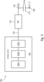
- FIG 4 is a schematic diagram 400 of a charge pump 402 and a floating filter including resistor 223 and capacitor 218 used in the differential PGA 200 of Figure 2 , according to an embodiment.
- Charge pump 402 can comprise a Dickson charge pump circuit comprising a plurality of charge pump stages 402A, 402B, and 402C. While three such stages are shown any number of stages can be used in embodiments.
- the charge pump stages can comprise either diode or transistor charge pump stages. Other types of charge pumps can also be used.
- An unfiltered charge pump output voltage is provided at node 225.
- a filtered charge pump voltage is provided at node 203 by the action of the low pass floating filter comprising biasing resistor R B1 223 and the charge pump capacitor C CHP 218, which can also be referred to herein as a "charge pump output capacitor” since it is coupled to the output of charge pump 402 through biasing resistor R B1 223.
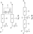
- FIGS 5A and 5B are schematic diagrams of alternative biasing arrangements for a MEMS device used with the differential PGA 200 shown in Figure 2 , according to embodiments. While the schematics shown in Figures 5A and 5B generally correspond to the differential PGA 200 shown in Figure 2 , many of the components of differential PGA 200 are omitted for the sake of clarity.
- a first biasing arrangement 500 is shown in Figure 5A , wherein a first voltage V MIC is applied to a first biasing resistor R B1 506 at node 502, and a second voltage V ASIC is applied to a second biasing resistor R B2 510 at node 504.
- the first voltage VMIC and the second voltage VASIC can be supplied by charge pumps of the type shown in Figure 4 .
- Biasing resistor 506 is coupled to node 508, which corresponds to node 203 in Figure 2
- biasing resistor 510 is coupled to node 514, which corresponds to node 202 in Figure 2
- a MEMS device 512 represented by capacitor C MEMS and voltage source V M
- a second biasing arrangement 550 is shown in Figure 5B , wherein the first biasing resistor RB1 is replaced by two biasing resistors R B1A 516 and R B1B 520 in series between nodes 502 and 508.
- a capacitor CMIC is coupled to the common node 518 between biasing resistors 516 and 520.
- the second biasing arrangement shown in Figure 5B provides additional filtering, and can also be used with respect to the second biasing resistor R B2 510, in some embodiments.
- FIG 6 is a schematic diagram of alternative source follower stage 600 including a transconductance stage 612, according to an embodiment, that can be used in the differential PGA 200 shown in Figure 2 .
- Source follower stage 600 includes P-channel transistor P1 having a source coupled to node 604 for providing an output voltage VOUT, a gate coupled to node 602 for receiving an input voltage VIN, and a drain coupled to node 606.
- a current source 608 is also coupled to node 606 for providing a bias current.
- a transconductance stage 612 has a negative input coupled to node 606, a positive input coupled to a reference voltage node 610, and an output coupled to node 604.
- FIG. 6 An equivalent model 614 is shown in Figure 6 , including a current source gm*Vgs in parallel with a resistor Ro.
- Figure 7 is a flowchart of a low noise amplification method 700, according to an embodiment, including, in a converter including a converter input, a first converter output, a second converter output, and an internal node, wherein the first converter output and the second converter output comprise a differential output, sensing an input voltage at the converter input at step 702; generating a noninverting first output voltage at the first converter output in response to the sensed input voltage 704; sensing the noninverting first output voltage at the first converter output at step 706; generating an inverting second output voltage at the second converter output in response to the noninverting first output voltage at step 708; coupling a charge pump output capacitor between the second converter output and the internal node at step 710; and coupling a feedback capacitor between the first converter output and the internal node at step 712.
- FIG 8 is a block diagram of a digital microphone product 800 including a low noise differential PGA as described above, according to an embodiment.
- Digital microphone product 800 includes MEMS device 802 and ASIC 804.
- MEMS device can comprise a capacitive MEMS device that generates an analog voltage in response to received sound waves.
- ASIC 804 can comprise the low noise differential PGA, an ADC, as well as other signal processing circuitry.
- the MEMS device 802 and ASIC 804 are in communication via bidirectional bus 810.
- MEMS device 802 and ASIC 804 can be packaged together to form a single digital product, such as a digital microphone.
- digital microphone product 800 can also include other digital and analog components 806, such as additional filters, amplifiers, and other similar components.
- the other digital and analog components 806 can communicate with MEMS device 802 through bidirectional bus 812.
- digital microphone product 800 can also include a microprocessor 808, which can communicate with ASIC 804 and the other digital and analog components 806 through bidirectional bus 814 and bidirectional bus 816.
- microprocessor 808 can generate clock signals and receive data from ASIC 804.
- microprocessor 808 can provide the functionality of digital or software components that would otherwise be resident on ASIC 804.
Landscapes
- Engineering & Computer Science (AREA)
- Power Engineering (AREA)
- Physics & Mathematics (AREA)
- Acoustics & Sound (AREA)
- Signal Processing (AREA)
- Health & Medical Sciences (AREA)
- General Health & Medical Sciences (AREA)
- Otolaryngology (AREA)
- Microelectronics & Electronic Packaging (AREA)
- Multimedia (AREA)
- Theoretical Computer Science (AREA)
- Amplifiers (AREA)
Abstract
Description
- The present invention relates generally to single-to-differential conversion in silicon microphone amplifiers, and to a corresponding system and method.
- Silicon based microphones (SiMic) or "digital microphones" are known in the art. Digital microphones typically include a microelectromechanical systems (MEMS) device responsive to sound waves for generating an analog signal, an amplifier such as a programmable gain amplifier (PGA) for amplifying the analog signal, an analog to digital converter (ADC) for converting the analog signal into a digital signal, and subsequent digital components for further processing of the digital signal. Single-ended and differential PGAs are also known in the art. The signal to noise ratio of the digital microphone can be adversely affected by noise generated in the PGA.
- According to an embodiment, a single-ended to differential converter includes a converter input, a first converter output, a second converter output, and an internal node, wherein the first converter output and the second converter output include a differential output; a non-inverting amplifier having an input coupled to the converter input, and an output coupled to the first converter output; an inverting amplifier having an input coupled to the first converter output, and an output coupled to the second converter output; a charge pump having a charge pump output capacitor coupled between the second converter output and the internal node; and a feedback capacitor coupled between the first converter output and the internal node. According to an embodiment, an integrated circuit includes a first converter pin, a first converter output, a second converter output, and a second converter pin, wherein the first converter output and the second converter output include a first differential output; a non-inverting amplifier having an input coupled to the first converter pin, and an output coupled to the first converter output; an inverting amplifier having an input coupled to the first converter output, and an output coupled to the second converter output; a charge pump having a charge pump output capacitor coupled between the second converter output and the second converter pin; and a feedback capacitor coupled between the first converter output and the second converter pin.
- According to an embodiment, a conversion method includes in a converter including a converter input, a first converter output, a second converter output, and an internal node, wherein the first converter output and the second converter output include a differential output, sensing an input voltage at the converter input; generating a noninverting first output voltage at the first converter output in response to the sensed input voltage; sensing the noninverting first output voltage at the first converter output; generating an inverting second output voltage at the second converter output in response to the noninverting first output voltage; coupling a charge pump output capacitor between the second converter output and the internal node; and coupling a feedback capacitor between the first converter output and the internal node.
- For a more complete understanding of the present invention, and the advantages thereof, reference is now made to the following descriptions taken in conjunction with the accompanying drawings, in which:
-
Figure 1 is a schematic diagram of an exemplary single-ended PGA for use in a digital microphone; -
Figure 2 is a schematic diagram of a differential PGA for use in a digital microphone, according to an embodiment; -
Figure 3 is a schematic diagram of an equivalent circuit of the differential PGA ofFigure 2 ; -
Figure 4 is a schematic diagram of a charge pump and a floating filter used in the differential PGA ofFigure 2 , according to an embodiment; -
Figures 5A and 5B are schematic diagrams of alternative biasing arrangements for a MEMS device used with the differential PGA shown inFigure 2 , according to embodiments; -
Figure 6 is a schematic diagram of alternative source follower stage including a transconductance stage; -
Figure 7 is a flowchart of a low noise amplification method, according to an embodiment; and -
Figure 8 is a block diagram of a digital microphone product, according to an embodiment. - The making and using of the presently preferred embodiments are discussed in detail below. It should be appreciated, however, that the present invention provides many applicable inventive concepts that can be embodied in a wide variety of specific contexts. The specific embodiments discussed are merely illustrative of specific ways to make and use the invention, and do not limit the scope of the invention.
- In the following detailed description, reference is made to the accompanying drawings, which form a part hereof and in which are shown by way of illustrations specific embodiments in which the invention may be practiced. It is to be understood that other embodiments may be utilized and structural or logical changes may be made without departing from the scope of the present invention. For example, features illustrated or described for one embodiment can be used on or in conjunction with other embodiments to yield yet a further embodiment. It is intended that the present invention includes such modifications and variations. The examples are described using specific language, which should not be construed as limiting the scope of the appending claims. The drawings are not scaled and are for illustrative purposes only. For clarity, the same or similar elements have been designated by corresponding references in the different drawings if not stated otherwise.
- Single-ended MEMs microphone signals can be converted to differential signals to ensure good power supply rejection (PSR) performance in the digital microphone. According to embodiment ideas, PGA gain is increased in the "frontend" of the digital microphone (as close to the input pin as possible) in order to maximize SNR. This is accomplished using an extremely low noise PGA amplifier that is described in detail below, according to embodiments.
- In operation, the low noise PGA amplifier combines a capacitive feedback source-follower-based PGA, together with an inverting stage which drives the "ground" of a charge pump filtering capacitance. In this way, the noise of the inverter stage becomes common mode and is cancelled out in a differential processing. In embodiments, the inverter stage can be a low-power inverter stage.
-
Figure 1 shows a simplified schematic of an exemplary single-ended source-follower-basedamplifier 100.Amplifier 100 includes a P-channel transistor P1 used in a source-follower configuration. The gate of transistor P1 is coupled toinput node 104, the source of transistor P1 is coupled to theoutput node 106, and the drain of transistor P1 is coupled to ground or other DC voltage source. A bias current source IBIAS is coupled tooutput node 106 for providing a bias current to transistor P1. The gate of transistor P1 is coupled to diodes D1 and D2 for clamping the input voltage ofamplifier 100. AMEMS device 108, which is represented by a capacitor CMEMS and an analog input voltage VIN, is coupled betweennode 102 andinput node 104. A feedback capacitor CFB is coupled betweennode 102 andoutput node 106, and a charge pump capacitor CCHP is coupled betweennode 102 and ground or another DC voltage source. Capacitor CCHP is used to filter out the charge-pump biasing voltage ripple of the unfiltered VMIC biasing voltage. Capacitors CFB and CCHP determine the gain ofamplifier 100, which is given by the equation VOUT = (1 + CFB/CCHP)∗VIN. - While
amplifier 100 shown inFigure 1 provide good performance for amplifying the analog signal of theMEMS device 108, the single-ended output can be converted to a differential output having improved noise performance in a differential PGA described in further detail below, according to embodiments. The differential PGA can be used in a digital microphone product having an improved SNR. -
Figure 2 is a schematic diagram of an improved noisedifferential PGA 200 having low noise performance, according to an embodiment. In PGA 200A, charge pump capacitor CCHP is boosted with the inverted output of an inverting amplifier in order to improve noise performance as will be explained in further detail below. Subsequent stages can be AC or DC coupled, can be programmable, and can be fully or pseudo-differential. While a single transistor source follower stage is shown inFigure 2 , other source follow topologies can be used for the source follower. -
PGA 200 includes a P-channel transistor PSF in a source-follower configuration having a source coupled to afirst output node 204 for providing the Vout_p output voltage, a gate coupled to input node 202, which is biased to the VASIC DC bias voltage, and a drain coupled to ground or to another DC voltage source. The source of transistor PSF is biased by the current provided bycurrent source 205. Capacitors CFB and CCHP determine the gain ofamplifier 100, which is given by the equation Vout_p = (1 + CFB/CCHP)∗VIN. Capacitor 220 (CFB) can be made adjustable, in an embodiment.Capacitor 220 is coupled betweennodes nodes 203 andnodes 206. AMEMS device 216, shown as a MEMS capacitor CMEMS and an input voltage VIN, is coupled betweennodes 202 and 203. A firstbiasing resistor R B1 223 is coupled betweennode 203 and a source ofbias voltage V B1 225. The VB1 bias voltage represents an unfiltered charge pump voltage VMIC, and the voltage atnode 203 represents the filtered charge pump voltage VMIC. A second biasing resistor RB2 is coupled between node 202 and a source ofbias voltage V B2 224. The VB2 bias voltage represents an unfiltered charge pump voltage VASIC, and the voltage at node 202 represents the filtered charge pump voltage VASIC. - The Vout_p output voltage is amplified by a unity gain inverting
operational amplifier 208 having a gain determined by the ratio ofresistors resistors resistors operational amplifier 208 provides the Vout_n output voltage atnode 206.Nodes -
PGA 200 includes a differential output circuit comprising a differential coupling circuit, a differential biasing circuit, and adifferential PGA stage 236. The differential coupling circuit comprises CAC coupling capacitor 226 coupled betweennode 204 and the negative input ofPGA stage 236, and CAC coupling capacitor 228 coupled betweennode 206 and the positive input ofPGA stage 236. The differential biasing circuit comprises a thirdbias resistor R BIAS 232 coupled between the negative input ofPGA stage 236 and a source of VBIAS bias voltage 230, and a fourthbias resistor R BIAS 234 coupled between the positive input ofPGA 236 and the source of VBIAS bias voltage 230.PGA 236 provides a second buffered differential output atnode 238 andnode 240. While a fully differential output circuit is shown inFigure 2 , other output circuits can be provided as previously discussed, including other fully differential output circuits, pseudo-differential output circuits, and even single-ended output circuits in embodiments. -
Figure 3 is a schematic diagram of anequivalent circuit 300 corresponding to the differential PGA ofFigure 2 including a unitygain noninverting amplifier 316 having an output coupled toVP node 304, and an invertingamplifier 318 coupled betweenVP node 304 andVN node 306. - The biasing resistors, MEMS device, and differential output circuit are omitted in
Figure 3 for the sake of clarity.Equivalent circuit 300 also includes afirst impedance Z1 310 that corresponds to charge pump capacitor CCHP previously discussed, and asecond impedance Z2 308 that corresponds to feedback capacitor CFB previously discussed.First impedance Z1 310 is coupled betweenVN node 306 andnode 312, andsecond impedance Z2 308 is coupled betweennode 312 andnode 314. A current "i" flows throughfirst impedance Z1 310 andsecond impedance Z2 308. Inequivalent circuit 300,voltage source VN1 302 represents the input voltage andvoltage source VN2 320 represents the noise voltage associated with invertingamplifier 318. The gain of the equivalent circuit is thus given by the equation (VP-VN) = VN1∗(1+Z2/Z1). From an inspection ofFigure 3 it can be noted that the noise voltage VN2 is subtracted out from the differential output voltage (VP-VN) as the noise voltage is a common mode voltage component, such that the overall noise component is lowered with respect to theamplifier 100 shown inFigure 1 . -
Figure 4 is a schematic diagram 400 of acharge pump 402 and a floatingfilter including resistor 223 andcapacitor 218 used in thedifferential PGA 200 ofFigure 2 , according to an embodiment.Charge pump 402 can comprise a Dickson charge pump circuit comprising a plurality of charge pump stages 402A, 402B, and 402C. While three such stages are shown any number of stages can be used in embodiments. The charge pump stages can comprise either diode or transistor charge pump stages. Other types of charge pumps can also be used. An unfiltered charge pump output voltage is provided atnode 225. A filtered charge pump voltage is provided atnode 203 by the action of the low pass floating filter comprising biasingresistor R B1 223 and the chargepump capacitor C CHP 218, which can also be referred to herein as a "charge pump output capacitor" since it is coupled to the output ofcharge pump 402 through biasingresistor R B1 223. -
Figures 5A and 5B are schematic diagrams of alternative biasing arrangements for a MEMS device used with thedifferential PGA 200 shown inFigure 2 , according to embodiments. While the schematics shown inFigures 5A and 5B generally correspond to thedifferential PGA 200 shown inFigure 2 , many of the components ofdifferential PGA 200 are omitted for the sake of clarity. Afirst biasing arrangement 500 is shown inFigure 5A , wherein a first voltage VMIC is applied to a firstbiasing resistor R B1 506 atnode 502, and a second voltage VASIC is applied to a secondbiasing resistor R B2 510 atnode 504. The first voltage VMIC and the second voltage VASIC can be supplied by charge pumps of the type shown inFigure 4 .Biasing resistor 506 is coupled tonode 508, which corresponds tonode 203 inFigure 2 , and biasingresistor 510 is coupled tonode 514, which corresponds to node 202 inFigure 2 . AMEMS device 512, represented by capacitor CMEMS and voltage source VM, is coupled betweennodes second biasing arrangement 550 is shown inFigure 5B , wherein the first biasing resistor RB1 is replaced by two biasingresistors R B1A 516 andR B1B 520 in series betweennodes common node 518 between biasingresistors Figure 5B provides additional filtering, and can also be used with respect to the secondbiasing resistor R B2 510, in some embodiments. -
Figure 6 is a schematic diagram of alternativesource follower stage 600 including atransconductance stage 612, according to an embodiment, that can be used in thedifferential PGA 200 shown inFigure 2 .Source follower stage 600 includes P-channel transistor P1 having a source coupled tonode 604 for providing an output voltage VOUT, a gate coupled tonode 602 for receiving an input voltage VIN, and a drain coupled tonode 606. Acurrent source 608 is also coupled tonode 606 for providing a bias current. Atransconductance stage 612 has a negative input coupled tonode 606, a positive input coupled to areference voltage node 610, and an output coupled tonode 604. Anequivalent model 614 is shown inFigure 6 , including a current source gm*Vgs in parallel with a resistor Ro. The gain ofsource follower stage 600 is thus given by the equation VOUT/VIN = gm∗Ro/(gm∗Ro + 1), which is approximately unity gain. -
Figure 7 is a flowchart of a lownoise amplification method 700, according to an embodiment, including, in a converter including a converter input, a first converter output, a second converter output, and an internal node, wherein the first converter output and the second converter output comprise a differential output, sensing an input voltage at the converter input atstep 702; generating a noninverting first output voltage at the first converter output in response to the sensedinput voltage 704; sensing the noninverting first output voltage at the first converter output atstep 706; generating an inverting second output voltage at the second converter output in response to the noninverting first output voltage atstep 708; coupling a charge pump output capacitor between the second converter output and the internal node atstep 710; and coupling a feedback capacitor between the first converter output and the internal node atstep 712. -
Figure 8 is a block diagram of adigital microphone product 800 including a low noise differential PGA as described above, according to an embodiment.Digital microphone product 800 includesMEMS device 802 and ASIC 804. MEMS device can comprise a capacitive MEMS device that generates an analog voltage in response to received sound waves. ASIC 804 can comprise the low noise differential PGA, an ADC, as well as other signal processing circuitry. - The
MEMS device 802 and ASIC 804 are in communication viabidirectional bus 810.MEMS device 802 and ASIC 804 can be packaged together to form a single digital product, such as a digital microphone. In some embodiments,digital microphone product 800 can also include other digital andanalog components 806, such as additional filters, amplifiers, and other similar components. The other digital andanalog components 806 can communicate withMEMS device 802 throughbidirectional bus 812. In some embodiments,digital microphone product 800 can also include amicroprocessor 808, which can communicate with ASIC 804 and the other digital andanalog components 806 throughbidirectional bus 814 andbidirectional bus 816. For example,microprocessor 808 can generate clock signals and receive data from ASIC 804. In other embodiments,microprocessor 808 can provide the functionality of digital or software components that would otherwise be resident on ASIC 804. - Example embodiments of the present invention are summarized here. Other embodiments can also be understood from the entirety of the specification and the claims filed herein.
- Example 1.According to an embodiment, a single-ended to differential converter includes a converter input, a first converter output, a second converter output, and an internal node, wherein the first converter output and the second converter output include a differential output; a non-inverting amplifier having an input coupled to the converter input, and an output coupled to the first converter output; an inverting amplifier having an input coupled to the first converter output, and an output coupled to the second converter output; a charge pump having a charge pump output capacitor coupled between the second converter output and the internal node; and a feedback capacitor coupled between the first converter output and the internal node.
- Example 2. The single-ended to differential converter of Example 1, wherein the non-inverting amplifier includes a source follower.
- Example 3. The single-ended to differential converter of any of the above examples, wherein the source follower includes a P-channel transistor.
- Example 4. The single-ended to differential converter of any of the above examples, further including a current source coupled to the first converter output.
- Example 5. The single-ended to differential converter of any of the above examples, further including a transconductance component coupled to the source follower.
- Example 6. The single-ended to differential converter of any of the above examples, wherein the inverting amplifier includes an operational amplifier having a first resistor coupled to an inverting input of the operational amplifier, and a second resistor coupled between the inverting input of the operational amplifier and an output of the operational amplifier.
- Example 7. The single-ended to differential converter of any of the above examples, wherein the first resistor and the second resistor have equal values.
- Example 8. The single-ended to differential converter of any of the above examples, wherein the charge pump is coupled to the internal node through a first bias resistor.
- Example 9. The single-ended to differential converter of any of the above examples, wherein the feedback capacitor includes an adjustable value capacitor.
- Example 10. The single-ended to differential converter of any of the above examples, further including a MEMS device coupled between the internal node and the converter input.
- Example 11. The single-ended to differential converter of any of the above examples, wherein the MEMS device includes a capacitive MEMS device configured for converting sound waves into an analog voltage.
- Example 12. The single-ended to differential converter of any of the above examples, further including a second bias resistor coupled to the converter input.
- Example 13. The single-ended to differential converter of any of the above examples, further including a differential bias circuit coupled between the first converter output and the second converter output.
- Example 14. The single-ended to differential converter of any of the above examples, wherein the differential bias circuit includes a third bias resistor and a fourth bias resistor, and wherein the third bias resistor and the fourth bias resistor have equal values.
- Example 15. The single-ended to differential converter of any of the above examples, further including a differential output amplifier coupled between the first converter output and the second converter output.
- Example 16. The single-ended to differential converter of any of the above examples, wherein the differential output amplifier includes a programmable gain amplifier.
- Example 17. According to an embodiment, an integrated circuit includes a first converter pin, a first converter output, a second converter output, and a second converter pin, wherein the first converter output and the second converter output include a first differential output; a non-inverting amplifier having an input coupled to the first converter pin, and an output coupled to the first converter output; an inverting amplifier having an input coupled to the first converter output, and an output coupled to the second converter output; a charge pump having a charge pump output capacitor coupled between the second converter output and the second converter pin; and a feedback capacitor coupled between the first converter output and the second converter pin.
- Example 18. The integrated circuit of Example 17, further including a differential input coupled between the first converter output and the second converter output, and a second differential output responsive to the differential input coupled between a third converter pin and a fourth converter pin.
- Example 19. According to an embodiment, a conversion method includes in a converter including a converter input, a first converter output, a second converter output, and an internal node, wherein the first converter output and the second converter output include a differential output, sensing an input voltage at the converter input; generating a noninverting first output voltage at the first converter output in response to the sensed input voltage; sensing the noninverting first output voltage at the first converter output; generating an inverting second output voltage at the second converter output in response to the noninverting first output voltage; coupling a charge pump output capacitor between the second converter output and the internal node; and coupling a feedback capacitor between the first converter output and the internal node.
- Example 20. The conversion method of Example 19, further including coupling a MEMS device between the second converter output and the internal node.
- While this invention has been described with reference to illustrative embodiments, this description is not intended to be construed in a limiting sense. Various modifications and combinations of the illustrative embodiments, as well as other embodiments of the invention, will be apparent to persons skilled in the art upon reference to the description. It is therefore intended that the appended claims encompass any such modifications or embodiments.
Claims (15)
- A single-ended to differential converter, comprising:a converter input, a first converter output, a second converter output, and an internal node, wherein the first converter output and the second converter output comprise a differential output;a non-inverting amplifier having an input coupled to the converter input, and an output coupled to the first converter output;an inverting amplifier having an input coupled to the first converter output, and an output coupled to the second converter output;a charge pump having a charge pump output capacitor coupled between the second converter output and the internal node; anda feedback capacitor coupled between the first converter output and the internal node.
- The single-ended to differential converter of claim 1, wherein the non-inverting amplifier comprises a source follower.
- The single-ended to differential converter of claim 2, wherein the source follower comprises a P-channel transistor.
- The single-ended to differential converter of claim 2 or 3, further comprising:a current source coupled to the first converter output, and/ora transconductance component coupled to the source follower.
- The single-ended to differential converter of any of claims 1 to 4, wherein the inverting amplifier comprises an operational amplifier having a first resistor coupled to an inverting input of the operational amplifier, and a second resistor coupled between the inverting input of the operational amplifier and an output of the operational amplifier, wherein, for example, the first resistor and the second resistor may have equal values.
- The single-ended to differential converter of any of claims 1 to 5, wherein the charge pump is coupled to the internal node through a first bias resistor.
- The single-ended to differential converter of any of claims 1 to 6, wherein the feedback capacitor comprises an adjustable value capacitor.
- The single-ended to differential converter of any of claims 1 to 7, further comprising a MEMS device coupled between the internal node and the converter input, wherein, for example, the MEMS device may comprise a capacitive MEMS device configured for converting sound waves into an analog voltage.
- The single-ended to differential converter of any of claims 1 to 8, further comprising a second bias resistor coupled to the converter input.
- The single-ended to differential converter of any of claims 1 to 9, further comprising a differential bias circuit coupled between the first converter output and the second converter output, wherein, for example, the differential bias circuit may comprise a third bias resistor and a fourth bias resistor, and wherein the third bias resistor and the fourth bias resistor may have equal values.
- The single-ended to differential converter of any of claims 1 to 10, further comprising a differential output amplifier coupled between the first converter output and the second converter output, wherein, for example, the differential output amplifier may comprise a programmable gain amplifier.
- An integrated circuit, comprising:a first converter pin, a first converter output, a second converter output, and a second converter pin, wherein the first converter output and the second converter output comprise a first differential output;a non-inverting amplifier having an input coupled to the first converter pin, and an output coupled to the first converter output;an inverting amplifier having an input coupled to the first converter output, and an output coupled to the second converter output;a charge pump having a charge pump output capacitor coupled between the second converter output and the second converter pin; anda feedback capacitor coupled between the first converter output and the second converter pin.
- The integrated circuit of claim 12, further comprising a differential input coupled between the first converter output and the second converter output, and a second differential output responsive to the differential input coupled between a third converter pin and a fourth converter pin.
- A conversion method, comprising:in a converter comprising a converter input, a first converter output, a second converter output, and an internal node, wherein the first converter output and the second converter output comprise a differential output,sensing an input voltage at the converter input;generating a noninverting first output voltage at the first converter output in response to the sensed input voltage;sensing the noninverting first output voltage at the first converter output;generating an inverting second output voltage at the second converter output in response to the noninverting first output voltage;coupling a charge pump output capacitor between the second converter output and the internal node; andcoupling a feedback capacitor between the first converter output and the internal node.
- The conversion method of claim 14, further comprising coupling a MEMS device between the second converter output and the internal node.
Applications Claiming Priority (1)
| Application Number | Priority Date | Filing Date | Title |
|---|---|---|---|
| US17/658,716 US11943592B2 (en) | 2022-04-11 | 2022-04-11 | Single to differential conversion in silicon microphone amplifiers |
Publications (1)
| Publication Number | Publication Date |
|---|---|
| EP4262086A1 true EP4262086A1 (en) | 2023-10-18 |
Family
ID=86006513
Family Applications (1)
| Application Number | Title | Priority Date | Filing Date |
|---|---|---|---|
| EP23167322.9A Pending EP4262086A1 (en) | 2022-04-11 | 2023-04-11 | Single to differential conversion in silicon microphone amplifiers |
Country Status (4)
| Country | Link |
|---|---|
| US (1) | US11943592B2 (en) |
| EP (1) | EP4262086A1 (en) |
| KR (1) | KR20230145928A (en) |
| CN (1) | CN116896341A (en) |
Citations (4)
| Publication number | Priority date | Publication date | Assignee | Title |
|---|---|---|---|---|
| US6057737A (en) * | 1998-10-14 | 2000-05-02 | Pritchard; Eric K. | Non-linear asymmetrical audio amplifiers |
| US20090316935A1 (en) * | 2004-02-09 | 2009-12-24 | Audioasics A/S | Digital microphone |
| US9143104B2 (en) * | 2012-03-16 | 2015-09-22 | Rohm Co., Ltd. | Audio signal processing circuit, car audio apparatus using the same, audio component apparatus, electronic device and output audio signal generating method |
| CN105898655A (en) * | 2016-06-08 | 2016-08-24 | 维沃移动通信有限公司 | Signal output circuit and mobile terminal |
Family Cites Families (7)
| Publication number | Priority date | Publication date | Assignee | Title |
|---|---|---|---|---|
| JP4654998B2 (en) * | 2005-11-08 | 2011-03-23 | 株式会社デンソー | Sample hold circuit and multiple D / A converter |
| ITUB20151133A1 (en) * | 2015-05-29 | 2016-11-29 | St Microelectronics Srl | DIFFERENTIAL AMPLIFIER CIRCUIT FOR A CAPACITIVE ACOUSTIC TRANSDUCER AND CORRESPONDING CAPACITIVE ACOUSTIC TRANSDUCER |
| IT201700100359A1 (en) * | 2017-09-07 | 2019-03-07 | St Microelectronics Srl | AMPLIFIER CIRCUIT, SYSTEM AND CORRESPONDING EQUIPMENT |
| US10531213B2 (en) * | 2018-03-29 | 2020-01-07 | Cirrus Logic, Inc. | MEMS transducer system |
| US10439572B1 (en) * | 2018-07-30 | 2019-10-08 | Analog Devices Global Unlimited Company | Analog-to-digital converter using discrete time comparator and switched capacitor charge pump |
| US11095303B1 (en) * | 2020-06-30 | 2021-08-17 | Dialog Semiconductor B.V. | Single-ended to differential circuit |
| US11984860B2 (en) * | 2021-06-23 | 2024-05-14 | Stmicroelectronics S.R.L. | Charge amplification circuits and methods |
-
2022
- 2022-04-11 US US17/658,716 patent/US11943592B2/en active Active
-
2023
- 2023-04-06 KR KR1020230045404A patent/KR20230145928A/en active Pending
- 2023-04-10 CN CN202310371720.8A patent/CN116896341A/en active Pending
- 2023-04-11 EP EP23167322.9A patent/EP4262086A1/en active Pending
Patent Citations (4)
| Publication number | Priority date | Publication date | Assignee | Title |
|---|---|---|---|---|
| US6057737A (en) * | 1998-10-14 | 2000-05-02 | Pritchard; Eric K. | Non-linear asymmetrical audio amplifiers |
| US20090316935A1 (en) * | 2004-02-09 | 2009-12-24 | Audioasics A/S | Digital microphone |
| US9143104B2 (en) * | 2012-03-16 | 2015-09-22 | Rohm Co., Ltd. | Audio signal processing circuit, car audio apparatus using the same, audio component apparatus, electronic device and output audio signal generating method |
| CN105898655A (en) * | 2016-06-08 | 2016-08-24 | 维沃移动通信有限公司 | Signal output circuit and mobile terminal |
Non-Patent Citations (1)
| Title |
|---|
| RAKSHITDATTA K S ET AL: "A 12.5 mW, 11.1 $\text{nV}/\sqrt{\text{Hz}}$, -115 dB THD, $ < 1\ \mu\text{s}$ Settling, 18 bit SAR ADC Driver in 0.6 $\mu\text{m}$ CMOS", 2 May 2016, IEEE TRANSACTIONS ON CIRCUITS AND SYSTEMS II: EXPRESS BRIEFS, IEEE, USA, PAGE(S) 443 - 447, ISSN: 1549-7747, XP011607870 * |
Also Published As
| Publication number | Publication date |
|---|---|
| KR20230145928A (en) | 2023-10-18 |
| CN116896341A (en) | 2023-10-17 |
| US20230328433A1 (en) | 2023-10-12 |
| US11943592B2 (en) | 2024-03-26 |
Similar Documents
| Publication | Publication Date | Title |
|---|---|---|
| US8610497B2 (en) | System and method for capacitive signal source amplifier | |
| CN108494370B (en) | Chopper stabilized instrumentation amplifier | |
| US20080310655A1 (en) | Programmable integrated microphone interface circuit | |
| JP2003110375A (en) | Self-operating pwm (pulse width modulation) amplifier | |
| US10536122B2 (en) | Amplifier circuit, corresponding system and device | |
| US10972059B2 (en) | MEMS sensor | |
| US20180270588A1 (en) | Mems transducer amplifiers | |
| US5258723A (en) | Integrated instrumentation amplifier with integrated frequency-compensating capacitance | |
| CN111585531B (en) | A DC coupled differential front end amplifier circuit | |
| US10797665B2 (en) | Programmable gain amplifier systems and methods | |
| US11943592B2 (en) | Single to differential conversion in silicon microphone amplifiers | |
| US20220353594A1 (en) | Single-ended readout of a differential mems device | |
| US20090140808A1 (en) | Gain control circuit | |
| CN119135093A (en) | An amplifier circuit for improving common mode rejection ratio | |
| US8279011B2 (en) | Amplifier circuit and method of signal amplification | |
| CN116436415A (en) | Low Noise Transimpedance Amplifier Applied in Sensor Analog Front End | |
| CN210042121U (en) | Microphone input circuit | |
| GB2621079A (en) | Operational amplifier for use in coulomb counter circuit | |
| CN109275071A (en) | Audio processing device, chip, system and method | |
| TWI922226B (en) | Multichannel instrument amplifier | |
| KR101183986B1 (en) | A read-out circuit with high impedance | |
| CN119945437A (en) | A high-precision accelerometer signal pseudo-differential digital conversion circuit and working method | |
| Dong et al. | Design of A Dual-Mode Analog Front-End Circuit Applied in the Voice Activity Detection System | |
| CN118449463A (en) | A Low Offset Chopper-Zero Operational Amplifier Circuit | |
| CN117213534A (en) | Photoelectric detection circuit and method integrating photoelectric detector and optical power meter |
Legal Events
| Date | Code | Title | Description |
|---|---|---|---|
| PUAI | Public reference made under article 153(3) epc to a published international application that has entered the european phase |
Free format text: ORIGINAL CODE: 0009012 |
|
| STAA | Information on the status of an ep patent application or granted ep patent |
Free format text: STATUS: THE APPLICATION HAS BEEN PUBLISHED |
|
| AK | Designated contracting states |
Kind code of ref document: A1 Designated state(s): AL AT BE BG CH CY CZ DE DK EE ES FI FR GB GR HR HU IE IS IT LI LT LU LV MC ME MK MT NL NO PL PT RO RS SE SI SK SM TR |
|
| STAA | Information on the status of an ep patent application or granted ep patent |
Free format text: STATUS: REQUEST FOR EXAMINATION WAS MADE |
|
| 17P | Request for examination filed |
Effective date: 20231215 |
|
| RBV | Designated contracting states (corrected) |
Designated state(s): AL AT BE BG CH CY CZ DE DK EE ES FI FR GB GR HR HU IE IS IT LI LT LU LV MC ME MK MT NL NO PL PT RO RS SE SI SK SM TR |