EP4261888A1 - Distributed electro-static discharge protection - Google Patents
Distributed electro-static discharge protection Download PDFInfo
- Publication number
- EP4261888A1 EP4261888A1 EP23165521.8A EP23165521A EP4261888A1 EP 4261888 A1 EP4261888 A1 EP 4261888A1 EP 23165521 A EP23165521 A EP 23165521A EP 4261888 A1 EP4261888 A1 EP 4261888A1
- Authority
- EP
- European Patent Office
- Prior art keywords
- esd clamp
- bank
- integrated circuit
- circuit layout
- clamp device
- Prior art date
- Legal status (The legal status is an assumption and is not a legal conclusion. Google has not performed a legal analysis and makes no representation as to the accuracy of the status listed.)
- Pending
Links
Images







Classifications
-
- H—ELECTRICITY
- H02—GENERATION; CONVERSION OR DISTRIBUTION OF ELECTRIC POWER
- H02H—EMERGENCY PROTECTIVE CIRCUIT ARRANGEMENTS
- H02H9/00—Emergency protective circuit arrangements for limiting excess current or voltage without disconnection
- H02H9/005—Emergency protective circuit arrangements for limiting excess current or voltage without disconnection avoiding undesired transient conditions
-
- H—ELECTRICITY
- H10—SEMICONDUCTOR DEVICES; ELECTRIC SOLID-STATE DEVICES NOT OTHERWISE PROVIDED FOR
- H10D—INORGANIC ELECTRIC SEMICONDUCTOR DEVICES
- H10D89/00—Aspects of integrated devices not covered by groups H10D84/00 - H10D88/00
- H10D89/60—Integrated devices comprising arrangements for electrical or thermal protection, e.g. protection circuits against electrostatic discharge [ESD]
- H10D89/601—Integrated devices comprising arrangements for electrical or thermal protection, e.g. protection circuits against electrostatic discharge [ESD] for devices having insulated gate electrodes, e.g. for IGFETs or IGBTs
- H10D89/931—Integrated devices comprising arrangements for electrical or thermal protection, e.g. protection circuits against electrostatic discharge [ESD] for devices having insulated gate electrodes, e.g. for IGFETs or IGBTs characterised by the dispositions of the protective arrangements
-
- H—ELECTRICITY
- H02—GENERATION; CONVERSION OR DISTRIBUTION OF ELECTRIC POWER
- H02H—EMERGENCY PROTECTIVE CIRCUIT ARRANGEMENTS
- H02H9/00—Emergency protective circuit arrangements for limiting excess current or voltage without disconnection
-
- H—ELECTRICITY
- H02—GENERATION; CONVERSION OR DISTRIBUTION OF ELECTRIC POWER
- H02H—EMERGENCY PROTECTIVE CIRCUIT ARRANGEMENTS
- H02H9/00—Emergency protective circuit arrangements for limiting excess current or voltage without disconnection
- H02H9/04—Emergency protective circuit arrangements for limiting excess current or voltage without disconnection responsive to excess voltage
- H02H9/045—Emergency protective circuit arrangements for limiting excess current or voltage without disconnection responsive to excess voltage adapted to a particular application and not provided for elsewhere
- H02H9/046—Emergency protective circuit arrangements for limiting excess current or voltage without disconnection responsive to excess voltage adapted to a particular application and not provided for elsewhere responsive to excess voltage appearing at terminals of integrated circuits
-
- H—ELECTRICITY
- H10—SEMICONDUCTOR DEVICES; ELECTRIC SOLID-STATE DEVICES NOT OTHERWISE PROVIDED FOR
- H10D—INORGANIC ELECTRIC SEMICONDUCTOR DEVICES
- H10D89/00—Aspects of integrated devices not covered by groups H10D84/00 - H10D88/00
- H10D89/10—Integrated device layouts
Definitions
- ESD electro-static discharge
- I/O input/output
- an integrated circuit layout comprising a first bank and a second bank.
- the first bank comprises a plurality of I/O circuits and at least one first ESD clamp device.
- the second bank comprises at least one second ESD clamp device, wherein the at least one second ESD clamp device is different in type from the at least one first ESD clamp device.
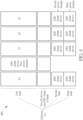
- FIG. 1 is a diagram illustrating an integrated circuit layout 100 according to a first embodiment of the present invention.
- the integrated circuit layout 100 has a rectangular-shaped design, and the integrated circuit layout 100 comprises a first bank and a second bank, wherein the first bank is arranged in an upper row, and the second bank is arranged in a lower row.
- the first bank comprises two power lines, which are used to provide two supply voltages DVDD and DVDD_IO for the circuits within the integrated circuit layout 100.
- the first bank comprises a plurality of I/O devices and at least one ESD clamp device
- the second bank comprises a plurality of ESD clamp devices
- the ESD clamp device in the first bank has a core device supplied by the supply voltage DVDD
- each of the ESD clamp devices in the second bank is an I/O device supplied by the supply voltage DVDD_IO.
- the I/O device and the core device the I/O device has a higher operating voltage, that is, can be operated by a higher supply voltage (i.e. the high-voltage device) .
- the core device has a lower operating voltage, that is, can be operated by a lower supply voltage (i.e. the low-voltage device).
- the distinction between the core device and the I/O device can be defined by a threshold voltage (Vth) of the transistor, a gate oxide thickness of the transistor, a junction breakdown voltage of the transistor, a well doping density of the transistor, a static leakage current of the transistor, or other suitable characteristics known in the semiconductor field.
- Vth threshold voltage
- a gate oxide thickness of the transistor a gate oxide thickness of the transistor
- a junction breakdown voltage of the transistor a well doping density of the transistor
- static leakage current of the transistor or other suitable characteristics known in the semiconductor field.
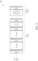
- FIG. 2 is a diagram illustrating an integrated circuit layout 200 according to a second embodiment of the present invention.
- the integrated circuit layout 200 has a rectangular-shaped design, and the integrated circuit layout 200 comprises a first bank, a second bank and a third bank, wherein the first bank is arranged in an upper row, the second bank is arranged in a middle row, and the third bank is arranged in a lower row.
- the first bank comprises a plurality of I/O devices and at least one ESD clamp device
- the second bank comprises a plurality of ESD clamp devices
- third bank comprises a plurality of ESD clamp devices
- the ESD clamp device in the first bank is powered by a first supply voltage belonging to a first power domain
- each ESD clamp device in the second bank is powered by a second supply voltage belonging to a second power domain
- each ESD clamp device in the third bank is powered by a third supply voltage belonging to a third power domain.
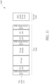
- FIG. 3 is a diagram illustrating an integrated circuit layout 300 according to a third embodiment of the present invention.
- the integrated circuit layout 300 has a rectangular-shaped design, and the integrated circuit layout 300 comprises a first bank and a second bank, wherein the first bank is arranged in an upper row, and the second bank is arranged in a lower row.
- the first bank comprises a plurality of I/O devices and at least one ESD clamp device
- the second bank comprises a plurality of ESD clamp devices
- the ESD clamp device in the first bank is powered by a first supply voltage DVDD1 belonging to a first power domain
- part of the ESD clamp devices in the second bank is/are powered by a second supply voltage DVDD2 belonging to a second power domain
- another part of the ESD clamp devices in the second bank is/are powered by a third supply voltage DVDD3 belonging to a third power domain.
- FIG. 4 is a diagram illustrating an integrated circuit layout 400 according to a fourth embodiment of the present invention.
- the integrated circuit layout 400 has a rectangular-shaped design, and the integrated circuit layout 400 comprises a first bank, a second bank and a third bank, wherein the first bank is arranged in a first row, the second bank is arranged in a third row, and the third bank is arranged in a fourth row, wherein the second row is used to place the non-I/O device, non-ESD clamp device, or leave blank.
- the first bank comprises a plurality of I/O devices and at least one ESD clamp device
- the second bank comprises a plurality of ESD clamp devices
- third bank comprises a plurality of ESD clamp devices
- the ESD clamp device in the first bank is powered by a first supply voltage belonging to a first power domain
- each ESD clamp device in the second bank is powered by a second supply voltage belonging to a second power domain
- each ESD clamp device in the third bank is powered by a third supply voltage belonging to a third power domain.
- FIG. 5 is a diagram illustrating an integrated circuit layout 500 according to a fifth embodiment of the present invention.
- the integrated circuit layout 500 has a rectangular-shaped design, and the integrated circuit layout 500 comprises a first bank and a second bank, wherein the first bank is arranged in an upper row, and the second bank is arranged in a lower row, wherein the middle row is used to place the non-I/O device, non-ESD clamp device, or leave blank.
- the first bank comprises a plurality of I/O devices and at least one ESD clamp device
- the second bank comprises a plurality of ESD clamp devices
- the ESD clamp device in the first bank is powered by a first supply voltage DVDD1 belonging to a first power domain
- part of the ESD clamp devices in the second bank is/are powered by a second supply voltage DVDD2 belonging to a second power domain
- another part of the ESD clamp devices in the second bank is/are powered by a third supply voltage DVDD3 belonging to a third power domain.
- the ESD clamp device layout will be more flexible for different circuit designs.
- FIG. 6 is a diagram illustrating an integrated circuit layout 600 according to a sixth embodiment of the present invention.
- the integrated circuit layout 600 comprises a first bank and a second bank, wherein the first bank is arranged in a lower row, and the second bank is arranged in an upper row.
- the first bank comprises a plurality of ESD clamp devices and a plurality of I/O pads, wherein the left and right sides of each I/O pad are immediately connected to the ESD clamp devices implemented by using I/O devices with high supply voltage such as 3.3V; and the second bank comprises two adjacent ESD clamp devices, wherein one of the ESD clamp devices is implemented by using core device (s) with lower supply voltage, and the other one of the ESD clamp devices is implemented by using I/O device(s) with the supply voltage such as 1.8V.
- FIG. 7 is a diagram illustrating an integrated circuit layout 700 according to a seventh embodiment of the present invention.
- the integrated circuit layout 700 has a rectangular-shaped design, and the integrated circuit layout 700 comprises a first bank and a second bank, wherein the first bank and the second bank are arranged in the same row.
- the first bank comprises a plurality of ESD clamp devices and a plurality of I/O pads, wherein the left and right sides of each I/O pad are immediately connected to the ESD clamp devices implemented by using I/O devices with high supply voltage such as 3.3V; and the second bank comprises two adjacent ESD clamp devices, wherein one of the ESD clamp devices is implemented by using core device (s) with lower supply voltage, and the other one of the ESD clamp devices is implemented by using I/O device(s) with the supply voltage such as 1.8V.
- the ESD clamp devices of the first bank and the ESD clamp devices of the second bank are from different I/O library, that is the ESD clamp devices have different schematics.
- FIG. 8 is a diagram illustrating an integrated circuit layout 800 according to an eighth embodiment of the present invention.
- the integrated circuit layout 800 has a rectangular-shaped design, and the integrated circuit layout 800 comprises a first bank and a second bank, wherein the first bank and the second bank are arranged in the same row.
- the first bank comprises a plurality of ESD clamp devices and a plurality of I/O pads, wherein the left and right sides of each I/O pad are immediately connected to the ESD clamp devices implemented by using I/O devices with high supply voltage such as 3.3V; and the second bank comprises two adjacent ESD clamp devices, wherein one of the ESD clamp devices is implemented by using core device (s) with lower supply voltage, and the other one of the ESD clamp devices is implemented by using I/O device(s) with the supply voltage such as 1.8V.
- the ESD clamp devices of the first bank and the ESD clamp devices of the second bank are from the same I/O library.
- the ESD clamp device layout will be more flexible for different circuit designs.
- FIG. 9 is a diagram illustrating an integrated circuit layout 900 according to a ninth embodiment of the present invention.
- the integrated circuit layout 900 comprises a first bank and a second bank, wherein the first bank is arranged in a lower row, and the second bank is arranged in an upper row.
- the first bank comprises a plurality of ESD clamp devices, at least one circuit module and a plurality of I/O pads, wherein part of the I/O pads are immediately connected to the ESD clamp devices implemented by using I/O devices; and the second bank comprises an ESD clamp device implemented by using core device(s).
- FIG. 10 is a diagram illustrating an integrated circuit layout 1000 according to a tenth embodiment of the present invention.
- the integrated circuit layout 1000 has a rectangular-shaped design, and the integrated circuit layout 1000 comprises a first bank and a second bank, wherein the first bank and the second bank are arranged in the same row.
- the first bank comprises a plurality of ESD clamp devices, at least one circuit module and a plurality of I/O pads, wherein part of the I/O pads are immediately connected to the ESD clamp devices implemented by using I/O devices; and the second bank comprises the ESD clamp devices implemented by using core device(s).
- the ESD clamp devices of the first bank and the ESD clamp devices of the second bank are from different I/O library, that is the ESD clamp devices have different schematics.
- FIG. 11 is a diagram illustrating an integrated circuit layout 1100 according to an eleventh embodiment of the present invention.
- the integrated circuit layout 1100 has a rectangular-shaped design, and the integrated circuit layout 1100 comprises a first bank and a second bank, wherein the first bank and the second bank are arranged in the same row.
- the first bank comprises a plurality of ESD clamp devices, at least one circuit module and a plurality of I/O pads, wherein part of the I/O pads are immediately connected to the ESD clamp devices implemented by using I/O devices; and the second bank comprises the ESD clamp devices implemented by using core device(s).
- the ESD clamp devices of the first bank and the ESD clamp devices of the second bank are from the same I/O library.
- FIG. 12 is a diagram illustrating an integrated circuit layout 1200 according to a twelfth embodiment of the present invention.
- the integrated circuit layout 1200 has a rectangular-shaped design, and the integrated circuit layout 1200 comprises a first bank and a second bank, wherein the first bank is arranged in a lower row, and the second bank is arranged in an upper row.
- the first bank comprises a plurality of ESD clamp devices, at least one circuit module and a plurality of I/O pads, wherein part of the I/O pads are immediately connected to the ESD clamp devices implemented by using I/O devices; and the second bank comprises an ESD clamp device implemented by using core device (s) .
- the ESD clamp devices of the first bank and the ESD clamp devices of the second bank are from different I/O library, that is, the ESD clamp devices have different schematics.
- the area between the ESD clamp device of the second bank and a dashed box 1202 can be blank or have other devices such as analog circuits or memory (i.e. non-I/O device, non-ESD clamp device).
- the ESD clamp device layout will be more flexible for different circuit designs.
Landscapes
- Engineering & Computer Science (AREA)
- Microelectronics & Electronic Packaging (AREA)
- Semiconductor Integrated Circuits (AREA)
- Design And Manufacture Of Integrated Circuits (AREA)
Abstract
Description
- This application claims the benefit of
U.S. Provisional Application No. 63/329,945, filed on April 12th, 2022 - In conventional integrated circuit layout having electro-static discharge (ESD) clamp devices, the ESD clamp devices and input/output (I/O) devices are served as a single bank and placed in a same row. However, this design is inflexible and may not be optimal for circuits of different designs.
- It is therefore an objective of the present invention to provide an integrated circuit layout in which the ESD clamp devices are divided into more banks with different configurations, to solve the above-mentioned problems.
- According to one embodiment of the present invention, an integrated circuit layout comprising a first bank and a second bank is disclosed. The first bank comprises a plurality of I/O circuits and at least one first ESD clamp device. The second bank comprises at least one second ESD clamp device, wherein the at least one second ESD clamp device is different in type from the at least one first ESD clamp device.
- These and other objectives of the present invention will no doubt become obvious to those of ordinary skill in the art after reading the following detailed description of the preferred embodiment that is illustrated in the various figures and drawings.
-
-
FIG. 1 is a diagram illustrating an integrated circuit layout according to a first embodiment of the present invention. -
FIG. 2 is a diagram illustrating an integrated circuit layout according to a second embodiment of the present invention. -
FIG. 3 is a diagram illustrating an integrated circuit layout according to a third embodiment of the present invention. -
FIG. 4 is a diagram illustrating an integrated circuit layout according to a fourth embodiment of the present invention. -
FIG. 5 is a diagram illustrating an integrated circuit layout according to a fifth embodiment of the present invention. -
FIG. 6 is a diagram illustrating an integrated circuit layout according to a sixth embodiment of the present invention. -
FIG. 7 is a diagram illustrating an integrated circuit layout according to a seventh embodiment of the present invention. -
FIG. 8 is a diagram illustrating an integrated circuit layout according to an eighth embodiment of the present invention. -
FIG. 9 is a diagram illustrating an integrated circuit layout according to a ninth embodiment of the present invention. -
FIG. 10 is a diagram illustrating an integrated circuit layout according to a tenth embodiment of the present invention. -
FIG. 11 is a diagram illustrating an integrated circuit layout according to an eleventh embodiment of the present invention. -
FIG. 12 is a diagram illustrating an integrated circuit layout according to a twelfth embodiment of the present invention. - Certain terms are used throughout the following description and claims to refer to particular system components. As one skilled in the art will appreciate, manufacturers may refer to a component by different names. This document does not intend to distinguish between components that differ in name but not function. In the following discussion and in the claims, the terms "including" and "comprising" are used in an open-ended fashion, and thus should be interpreted to mean "including, but not limited to ...". The terms "couple" and "couples" are intended to mean either an indirect or a direct electrical connection. Thus, if a first device couples to a second device, that connection may be through a direct electrical connection, or through an indirect electrical connection via other devices and connections.
-
FIG. 1 is a diagram illustrating anintegrated circuit layout 100 according to a first embodiment of the present invention. As shown inFIG. 1 , theintegrated circuit layout 100 has a rectangular-shaped design, and theintegrated circuit layout 100 comprises a first bank and a second bank, wherein the first bank is arranged in an upper row, and the second bank is arranged in a lower row. In this embodiment, the first bank comprises two power lines, which are used to provide two supply voltages DVDD and DVDD_IO for the circuits within theintegrated circuit layout 100. In addition, the first bank comprises a plurality of I/O devices and at least one ESD clamp device, and the second bank comprises a plurality of ESD clamp devices, wherein the ESD clamp device in the first bank has a core device supplied by the supply voltage DVDD, and each of the ESD clamp devices in the second bank is an I/O device supplied by the supply voltage DVDD_IO. Regarding the I/O device and the core device, the I/O device has a higher operating voltage, that is, can be operated by a higher supply voltage (i.e. the high-voltage device) . On the other hand, the core device has a lower operating voltage, that is, can be operated by a lower supply voltage (i.e. the low-voltage device). Please note that those skilled in this art will readily understand that the distinction between the core device and the I/O device can be defined by a threshold voltage (Vth) of the transistor, a gate oxide thickness of the transistor, a junction breakdown voltage of the transistor, a well doping density of the transistor, a static leakage current of the transistor, or other suitable characteristics known in the semiconductor field. -
FIG. 2 is a diagram illustrating anintegrated circuit layout 200 according to a second embodiment of the present invention. As shown inFIG. 2 , theintegrated circuit layout 200 has a rectangular-shaped design, and theintegrated circuit layout 200 comprises a first bank, a second bank and a third bank, wherein the first bank is arranged in an upper row, the second bank is arranged in a middle row, and the third bank is arranged in a lower row. In this embodiment, the first bank comprises a plurality of I/O devices and at least one ESD clamp device, the second bank comprises a plurality of ESD clamp devices, and third bank comprises a plurality of ESD clamp devices, wherein the ESD clamp device in the first bank is powered by a first supply voltage belonging to a first power domain, each ESD clamp device in the second bank is powered by a second supply voltage belonging to a second power domain, and each ESD clamp device in the third bank is powered by a third supply voltage belonging to a third power domain. -
FIG. 3 is a diagram illustrating anintegrated circuit layout 300 according to a third embodiment of the present invention. As shown inFIG. 3 , theintegrated circuit layout 300 has a rectangular-shaped design, and theintegrated circuit layout 300 comprises a first bank and a second bank, wherein the first bank is arranged in an upper row, and the second bank is arranged in a lower row. In this embodiment, the first bank comprises a plurality of I/O devices and at least one ESD clamp device, and the second bank comprises a plurality of ESD clamp devices, wherein the ESD clamp device in the first bank is powered by a first supply voltage DVDD1 belonging to a first power domain, part of the ESD clamp devices in the second bank is/are powered by a second supply voltage DVDD2 belonging to a second power domain, and another part of the ESD clamp devices in the second bank is/are powered by a third supply voltage DVDD3 belonging to a third power domain. -
FIG. 4 is a diagram illustrating anintegrated circuit layout 400 according to a fourth embodiment of the present invention. As shown inFIG. 4 , theintegrated circuit layout 400 has a rectangular-shaped design, and theintegrated circuit layout 400 comprises a first bank, a second bank and a third bank, wherein the first bank is arranged in a first row, the second bank is arranged in a third row, and the third bank is arranged in a fourth row, wherein the second row is used to place the non-I/O device, non-ESD clamp device, or leave blank. In this embodiment, the first bank comprises a plurality of I/O devices and at least one ESD clamp device, the second bank comprises a plurality of ESD clamp devices, and third bank comprises a plurality of ESD clamp devices, wherein the ESD clamp device in the first bank is powered by a first supply voltage belonging to a first power domain, each ESD clamp device in the second bank is powered by a second supply voltage belonging to a second power domain, and each ESD clamp device in the third bank is powered by a third supply voltage belonging to a third power domain. -
FIG. 5 is a diagram illustrating anintegrated circuit layout 500 according to a fifth embodiment of the present invention. As shown inFIG. 5 , theintegrated circuit layout 500 has a rectangular-shaped design, and theintegrated circuit layout 500 comprises a first bank and a second bank, wherein the first bank is arranged in an upper row, and the second bank is arranged in a lower row, wherein the middle row is used to place the non-I/O device, non-ESD clamp device, or leave blank. In this embodiment, the first bank comprises a plurality of I/O devices and at least one ESD clamp device, and the second bank comprises a plurality of ESD clamp devices, wherein the ESD clamp device in the first bank is powered by a first supply voltage DVDD1 belonging to a first power domain, part of the ESD clamp devices in the second bank is/are powered by a second supply voltage DVDD2 belonging to a second power domain, and another part of the ESD clamp devices in the second bank is/are powered by a third supply voltage DVDD3 belonging to a third power domain. - In the embodiments shown in
FIG. 1 - FIG. 5 , by arranging the ESD clamp devices in different rows, the ESD clamp device layout will be more flexible for different circuit designs. -
FIG. 6 is a diagram illustrating anintegrated circuit layout 600 according to a sixth embodiment of the present invention. As shown inFIG. 6 , theintegrated circuit layout 600 comprises a first bank and a second bank, wherein the first bank is arranged in a lower row, and the second bank is arranged in an upper row. In this embodiment, the first bank comprises a plurality of ESD clamp devices and a plurality of I/O pads, wherein the left and right sides of each I/O pad are immediately connected to the ESD clamp devices implemented by using I/O devices with high supply voltage such as 3.3V; and the second bank comprises two adjacent ESD clamp devices, wherein one of the ESD clamp devices is implemented by using core device (s) with lower supply voltage, and the other one of the ESD clamp devices is implemented by using I/O device(s) with the supply voltage such as 1.8V. -
FIG. 7 is a diagram illustrating anintegrated circuit layout 700 according to a seventh embodiment of the present invention. As shown inFIG. 7 , theintegrated circuit layout 700 has a rectangular-shaped design, and theintegrated circuit layout 700 comprises a first bank and a second bank, wherein the first bank and the second bank are arranged in the same row. In this embodiment, the first bank comprises a plurality of ESD clamp devices and a plurality of I/O pads, wherein the left and right sides of each I/O pad are immediately connected to the ESD clamp devices implemented by using I/O devices with high supply voltage such as 3.3V; and the second bank comprises two adjacent ESD clamp devices, wherein one of the ESD clamp devices is implemented by using core device (s) with lower supply voltage, and the other one of the ESD clamp devices is implemented by using I/O device(s) with the supply voltage such as 1.8V. In addition, the ESD clamp devices of the first bank and the ESD clamp devices of the second bank are from different I/O library, that is the ESD clamp devices have different schematics. -
FIG. 8 is a diagram illustrating anintegrated circuit layout 800 according to an eighth embodiment of the present invention. As shown inFIG. 8 , theintegrated circuit layout 800 has a rectangular-shaped design, and theintegrated circuit layout 800 comprises a first bank and a second bank, wherein the first bank and the second bank are arranged in the same row. In this embodiment, the first bank comprises a plurality of ESD clamp devices and a plurality of I/O pads, wherein the left and right sides of each I/O pad are immediately connected to the ESD clamp devices implemented by using I/O devices with high supply voltage such as 3.3V; and the second bank comprises two adjacent ESD clamp devices, wherein one of the ESD clamp devices is implemented by using core device (s) with lower supply voltage, and the other one of the ESD clamp devices is implemented by using I/O device(s) with the supply voltage such as 1.8V. In addition, the ESD clamp devices of the first bank and the ESD clamp devices of the second bank are from the same I/O library. - In the embodiments shown in
FIG. 6 - FIG. 8 , by dividing the ESD clamp devices with different types to different banks, the ESD clamp device layout will be more flexible for different circuit designs. -
FIG. 9 is a diagram illustrating anintegrated circuit layout 900 according to a ninth embodiment of the present invention. As shown inFIG. 9 , theintegrated circuit layout 900 comprises a first bank and a second bank, wherein the first bank is arranged in a lower row, and the second bank is arranged in an upper row. In this embodiment, the first bank comprises a plurality of ESD clamp devices, at least one circuit module and a plurality of I/O pads, wherein part of the I/O pads are immediately connected to the ESD clamp devices implemented by using I/O devices; and the second bank comprises an ESD clamp device implemented by using core device(s). -
FIG. 10 is a diagram illustrating anintegrated circuit layout 1000 according to a tenth embodiment of the present invention. As shown inFIG. 10 , theintegrated circuit layout 1000 has a rectangular-shaped design, and theintegrated circuit layout 1000 comprises a first bank and a second bank, wherein the first bank and the second bank are arranged in the same row. In this embodiment, the first bank comprises a plurality of ESD clamp devices, at least one circuit module and a plurality of I/O pads, wherein part of the I/O pads are immediately connected to the ESD clamp devices implemented by using I/O devices; and the second bank comprises the ESD clamp devices implemented by using core device(s). In addition, the ESD clamp devices of the first bank and the ESD clamp devices of the second bank are from different I/O library, that is the ESD clamp devices have different schematics. -
FIG. 11 is a diagram illustrating anintegrated circuit layout 1100 according to an eleventh embodiment of the present invention. As shown inFIG. 11 , theintegrated circuit layout 1100 has a rectangular-shaped design, and theintegrated circuit layout 1100 comprises a first bank and a second bank, wherein the first bank and the second bank are arranged in the same row. In this embodiment, the first bank comprises a plurality of ESD clamp devices, at least one circuit module and a plurality of I/O pads, wherein part of the I/O pads are immediately connected to the ESD clamp devices implemented by using I/O devices; and the second bank comprises the ESD clamp devices implemented by using core device(s). In addition, the ESD clamp devices of the first bank and the ESD clamp devices of the second bank are from the same I/O library. -
FIG. 12 is a diagram illustrating anintegrated circuit layout 1200 according to a twelfth embodiment of the present invention. As shown inFIG. 12 , theintegrated circuit layout 1200 has a rectangular-shaped design, and theintegrated circuit layout 1200 comprises a first bank and a second bank, wherein the first bank is arranged in a lower row, and the second bank is arranged in an upper row. In this embodiment, the first bank comprises a plurality of ESD clamp devices, at least one circuit module and a plurality of I/O pads, wherein part of the I/O pads are immediately connected to the ESD clamp devices implemented by using I/O devices; and the second bank comprises an ESD clamp device implemented by using core device (s) . In addition, the ESD clamp devices of the first bank and the ESD clamp devices of the second bank are from different I/O library, that is, the ESD clamp devices have different schematics. Furthermore, the area between the ESD clamp device of the second bank and a dashedbox 1202 can be blank or have other devices such as analog circuits or memory (i.e. non-I/O device, non-ESD clamp device). - In the embodiments shown in
FIG. 9 - FIG. 12 , by dividing the ESD clamp devices with different types to different banks, the ESD clamp device layout will be more flexible for different circuit designs. - Those skilled in the art will readily observe that numerous modifications and alterations of the device and method may be made while retaining the teachings of the invention. Accordingly, the above disclosure should be construed as limited only by the metes and bounds of the appended claims.
Claims (14)
- An integrated circuit layout (100, 200, 300, 400, 500, 600, 700, 800, 900, 1000, 1100, 1200), comprising:a first bank, comprising a plurality of input/output, I/O, circuits and at least one first electro-static discharge, ESD, clamp device; anda second bank, comprising at least one second ESD clamp device, wherein the at least one second ESD clamp device is different in type from the at least one first ESD clamp device.
- The integrated circuit layout (100, 200, 300, 400, 500, 600, 700, 800, 900, 1000, 1100, 1200) of claim 1, wherein the first bank is arranged in a first row of the integrated circuit layout (100, 200, 300, 400, 500, 600, 700, 800, 900, 1000, 1100, 1200), the second bank is arranged in a second row of the integrated circuit layout (100, 200, 300, 400, 500, 600, 700, 800, 900, 1000, 1100, 1200).
- The integrated circuit layout (100, 200, 300, 400, 500, 600, 700, 800, 900, 1000, 1100, 1200) of claim 2, wherein the at least one first ESD clamp devices are implemented by using core device (s), and the at least one second ESD clamp device is implemented by using I/O device(s).
- The integrated circuit layout (100, 200, 300, 400, 500, 600, 700, 800, 900, 1000, 1100, 1200) of claim 2, further comprising:a third bank, comprising at least one third ESD clamp device, wherein the third is arranged in a third row of the integrated circuit layout (100, 200, 300, 400, 500, 600, 700, 800, 900, 1000, 1100, 1200);wherein the at least one first ESD clamp device is powered by a first supply voltage belonging to a first power domain, the at least one second ESD clamp device is powered by a second supply voltage belonging to a second power domain, and the at least one third ESD clamp device is powered by a third supply voltage belonging to a third power domain.
- The integrated circuit layout (100, 200, 300, 400, 500, 600, 700, 800, 900, 1000, 1100, 1200) of claim 4, wherein the third row is adjacent to the second row of the integrated circuit layout (100, 200, 300, 400, 500, 600, 700, 800, 900, 1000, 1100, 1200), and there is a row comprising non-I/O devices or non-ESD clamp cells between the first row and the second row of the integrated circuit layout (100, 200, 300, 400, 500, 600, 700, 800, 900, 1000, 1100, 1200) .
- The integrated circuit layout (100, 200, 300, 400, 500, 600, 700, 800, 900, 1000, 1100, 1200) of claim 2, wherein the second bank comprises the at least one second ESD clamp device and at least one third ESD clamp device, and the at least one third ESD clamp device is different in type from the at least one second ESD clamp device.
- The integrated circuit layout (100, 200, 300, 400, 500, 600, 700, 800, 900, 1000, 1100, 1200) of claim 6, wherein the at least one first ESD clamp device is powered by a first supply voltage belonging to a first power domain, the at least one second ESD clamp device is powered by a second supply voltage belonging to a second power domain, and the at least one third ESD clamp device is powered by a third supply voltage belonging to a third power domain.
- The integrated circuit layout (100, 200, 300, 400, 500, 600, 700, 800, 900, 1000, 1100, 1200) of claim 6, wherein there is a row comprising non-I/O devices or non-ESD clamp cells between the first row and the second row of the integrated circuit layout (100, 200, 300, 400, 500, 600, 700, 800, 900, 1000, 1100, 1200).
- The integrated circuit layout (100, 200, 300, 400, 500, 600, 700, 800, 900, 1000, 1100, 1200) of claim 1, wherein the second bank comprises the at least one second ESD clamp device and at least one third ESD clamp device, the at least one first ESD clamp device is implemented by using first I/O device(s), the at least one second ESD clamp device is implemented by using second I/O device(s), and the at least one third ESD clamp device is implemented by using core device(s).
- The integrated circuit layout (100, 200, 300, 400, 500, 600, 700, 800, 900, 1000, 1100, 1200) of claim 9, wherein the first bank comprises the plurality of I/O circuits and a plurality of first ESD clamp devices, and left and right sides of each I/O pad are immediately connected to the first ESD clamp devices implemented.
- The integrated circuit layout (100, 200, 300, 400, 500, 600, 700, 800, 900, 1000, 1100, 1200) of claim 9, wherein the second I/O device(s) and the first I/O device(s) are from different I/O libraries.
- The integrated circuit layout (100, 200, 300, 400, 500, 600, 700, 800, 900, 1000, 1100, 1200) of claim 1, wherein the at least one first ESD clamp device is implemented by using first I/O device (s), and the at least one second ESD clamp device is implemented by using core device(s).
- The integrated circuit layout (100, 200, 300, 400, 500, 600, 700, 800, 900, 1000, 1100, 1200) of claim 12, wherein the second I/O device(s) and the first I/O device(s) are from different I/O libraries.
- The integrated circuit layout (100, 200, 300, 400, 500, 600, 700, 800, 900, 1000, 1100, 1200) of claim 12, wherein there is a row comprising non-I/O devices or non-ESD clamp cells between the first bank and the second bank.
Applications Claiming Priority (2)
| Application Number | Priority Date | Filing Date | Title |
|---|---|---|---|
| US202263329945P | 2022-04-12 | 2022-04-12 | |
| US18/123,344 US12388252B2 (en) | 2022-04-12 | 2023-03-20 | Distributed electro-static discharge protection |
Publications (1)
| Publication Number | Publication Date |
|---|---|
| EP4261888A1 true EP4261888A1 (en) | 2023-10-18 |
Family
ID=85792023
Family Applications (1)
| Application Number | Title | Priority Date | Filing Date |
|---|---|---|---|
| EP23165521.8A Pending EP4261888A1 (en) | 2022-04-12 | 2023-03-30 | Distributed electro-static discharge protection |
Country Status (3)
| Country | Link |
|---|---|
| US (1) | US12388252B2 (en) |
| EP (1) | EP4261888A1 (en) |
| TW (1) | TWI851129B (en) |
Citations (4)
| Publication number | Priority date | Publication date | Assignee | Title |
|---|---|---|---|---|
| US20080062596A1 (en) * | 2006-08-31 | 2008-03-13 | Freescale Semiconductor, Inc. | Distributed electrostatic discharge protection circuit with varying clamp size |
| JP2013021249A (en) * | 2011-07-14 | 2013-01-31 | Toshiba Corp | Semiconductor integrated device |
| US20150349522A1 (en) * | 2014-05-28 | 2015-12-03 | James W. Miller | Electrostatic discharge protection system |
| US20160086935A1 (en) * | 2014-09-24 | 2016-03-24 | Kabushiki Kaisha Toshiba | Semiconductor device |
Family Cites Families (10)
| Publication number | Priority date | Publication date | Assignee | Title |
|---|---|---|---|---|
| JPH06105757B2 (en) * | 1987-02-13 | 1994-12-21 | 富士通株式会社 | Master slice type semiconductor integrated circuit |
| JP2004296998A (en) * | 2003-03-28 | 2004-10-21 | Matsushita Electric Ind Co Ltd | Semiconductor device |
| US7593202B2 (en) | 2005-11-01 | 2009-09-22 | Freescale Semiconductor, Inc. | Electrostatic discharge (ESD) protection circuit for multiple power domain integrated circuit |
| US7872283B2 (en) * | 2006-11-09 | 2011-01-18 | Panasonic Corporation | Semiconductor integrated circuit and multi-chip module |
| US9076656B2 (en) | 2013-05-02 | 2015-07-07 | Freescale Semiconductor, Inc. | Electrostatic discharge (ESD) clamp circuit with high effective holding voltage |
| US9064938B2 (en) * | 2013-05-30 | 2015-06-23 | Freescale Semiconductor, Inc. | I/O cell ESD system |
| US9537308B2 (en) * | 2013-12-03 | 2017-01-03 | Lattice Semiconductor Corporation | ESD protection using shared RC trigger |
| DE102021100605A1 (en) | 2020-03-27 | 2021-09-30 | Taiwan Semiconductor Manufacturing Co., Ltd. | SNAPBACK ESD CIRCUIT, SYSTEM AND THEIR MANUFACTURING METHOD |
| US11418024B2 (en) * | 2020-06-09 | 2022-08-16 | Western Digital Technologies, Inc. | Electrostatic discharge circuit using booster cell |
| CN114696305A (en) * | 2020-12-29 | 2022-07-01 | 恩智浦有限公司 | Electrostatic discharge ESD protection device |
-
2023
- 2023-03-20 US US18/123,344 patent/US12388252B2/en active Active
- 2023-03-30 EP EP23165521.8A patent/EP4261888A1/en active Pending
- 2023-04-07 TW TW112112983A patent/TWI851129B/en active
Patent Citations (4)
| Publication number | Priority date | Publication date | Assignee | Title |
|---|---|---|---|---|
| US20080062596A1 (en) * | 2006-08-31 | 2008-03-13 | Freescale Semiconductor, Inc. | Distributed electrostatic discharge protection circuit with varying clamp size |
| JP2013021249A (en) * | 2011-07-14 | 2013-01-31 | Toshiba Corp | Semiconductor integrated device |
| US20150349522A1 (en) * | 2014-05-28 | 2015-12-03 | James W. Miller | Electrostatic discharge protection system |
| US20160086935A1 (en) * | 2014-09-24 | 2016-03-24 | Kabushiki Kaisha Toshiba | Semiconductor device |
Also Published As
| Publication number | Publication date |
|---|---|
| TWI851129B (en) | 2024-08-01 |
| US20230327428A1 (en) | 2023-10-12 |
| US12388252B2 (en) | 2025-08-12 |
| TW202341002A (en) | 2023-10-16 |
Similar Documents
| Publication | Publication Date | Title |
|---|---|---|
| CN102903715B (en) | Semiconductor integrated circuit | |
| US6815775B2 (en) | ESD protection design with turn-on restraining method and structures | |
| JP3992855B2 (en) | Circuit for electrostatic discharge protection | |
| US6040968A (en) | EOS/ESD protection for high density integrated circuits | |
| KR20240045354A (en) | Semiconductor layout in finfet technologies | |
| US5903419A (en) | Circuit for electrostatic discharge (ESD) protection | |
| JPH11135723A (en) | Cascode connection MOS ESD protection circuit for mixed voltage chip | |
| US8208234B2 (en) | Circuit with ESD protection for a switching regulator | |
| US20070236843A1 (en) | Floating gate structure with high electrostatic discharge performance | |
| JP6512520B2 (en) | Semiconductor device and design method thereof | |
| US20220294211A1 (en) | Failsafe Input/Output Electrostatic Discharge Protection With Diodes | |
| JPH08321586A (en) | Integrated semiconductor circuit | |
| US20020075034A1 (en) | Arrangement for improving the ESD protection in a CMOS buffer | |
| US12388252B2 (en) | Distributed electro-static discharge protection | |
| US8169758B2 (en) | Path sharing high-voltage ESD protection using distributed low-voltage clamps | |
| EP0730301A2 (en) | ESD protection device | |
| CN116504778B (en) | A high voltage ESD electrostatic layout structure | |
| EP0606667A1 (en) | Semiconductor device with an integrated circuit provided with over voltage protection means | |
| US6477023B1 (en) | Electrostatic discharge protection apparatus | |
| US20050002141A1 (en) | Electrostatic discharge protection circuit | |
| CN116387309A (en) | Electrostatic surge protection circuit suitable for load switch chip | |
| KR100357191B1 (en) | ESD protection circuit using metal coupling capacitor | |
| CN116913914A (en) | Integrated circuit layout and semiconductor die | |
| JP3037138B2 (en) | Electrostatic protection device for semiconductor integrated circuit | |
| US7248450B1 (en) | Pad cell with multiple signal paths |
Legal Events
| Date | Code | Title | Description |
|---|---|---|---|
| PUAI | Public reference made under article 153(3) epc to a published international application that has entered the european phase |
Free format text: ORIGINAL CODE: 0009012 |
|
| STAA | Information on the status of an ep patent application or granted ep patent |
Free format text: STATUS: THE APPLICATION HAS BEEN PUBLISHED |
|
| AK | Designated contracting states |
Kind code of ref document: A1 Designated state(s): AL AT BE BG CH CY CZ DE DK EE ES FI FR GB GR HR HU IE IS IT LI LT LU LV MC ME MK MT NL NO PL PT RO RS SE SI SK SM TR |
|
| STAA | Information on the status of an ep patent application or granted ep patent |
Free format text: STATUS: REQUEST FOR EXAMINATION WAS MADE |
|
| 17P | Request for examination filed |
Effective date: 20240412 |
|
| RBV | Designated contracting states (corrected) |
Designated state(s): AL AT BE BG CH CY CZ DE DK EE ES FI FR GB GR HR HU IE IS IT LI LT LU LV MC ME MK MT NL NO PL PT RO RS SE SI SK SM TR |
|
| STAA | Information on the status of an ep patent application or granted ep patent |
Free format text: STATUS: EXAMINATION IS IN PROGRESS |
|
| 17Q | First examination report despatched |
Effective date: 20251015 |