EP4261881A1 - Semiconductor package comprising an external lead with a barb portion and method of fabricating the same - Google Patents
Semiconductor package comprising an external lead with a barb portion and method of fabricating the same Download PDFInfo
- Publication number
- EP4261881A1 EP4261881A1 EP22167633.1A EP22167633A EP4261881A1 EP 4261881 A1 EP4261881 A1 EP 4261881A1 EP 22167633 A EP22167633 A EP 22167633A EP 4261881 A1 EP4261881 A1 EP 4261881A1
- Authority
- EP
- European Patent Office
- Prior art keywords
- semiconductor package
- external leads
- hole
- circuit board
- printed circuit
- Prior art date
- Legal status (The legal status is an assumption and is not a legal conclusion. Google has not performed a legal analysis and makes no representation as to the accuracy of the status listed.)
- Granted
Links
Images


Classifications
-
- H—ELECTRICITY
- H10—SEMICONDUCTOR DEVICES; ELECTRIC SOLID-STATE DEVICES NOT OTHERWISE PROVIDED FOR
- H10W—GENERIC PACKAGES, INTERCONNECTIONS, CONNECTORS OR OTHER CONSTRUCTIONAL DETAILS OF DEVICES COVERED BY CLASS H10
- H10W70/00—Package substrates; Interposers; Redistribution layers [RDL]
- H10W70/40—Leadframes
- H10W70/421—Shapes or dispositions
- H10W70/424—Cross-sectional shapes
- H10W70/427—Bent parts
- H10W70/429—Bent parts being the outer leads
-
- H—ELECTRICITY
- H05—ELECTRIC TECHNIQUES NOT OTHERWISE PROVIDED FOR
- H05K—PRINTED CIRCUITS; CASINGS OR CONSTRUCTIONAL DETAILS OF ELECTRIC APPARATUS; MANUFACTURE OF ASSEMBLAGES OF ELECTRICAL COMPONENTS
- H05K3/00—Apparatus or processes for manufacturing printed circuits
- H05K3/30—Assembling printed circuits with electric components, e.g. with resistors
- H05K3/306—Assembling printed circuits with electric components, e.g. with resistors with lead-in-hole components
- H05K3/308—Adaptations of leads
-
- H—ELECTRICITY
- H05—ELECTRIC TECHNIQUES NOT OTHERWISE PROVIDED FOR
- H05K—PRINTED CIRCUITS; CASINGS OR CONSTRUCTIONAL DETAILS OF ELECTRIC APPARATUS; MANUFACTURE OF ASSEMBLAGES OF ELECTRICAL COMPONENTS
- H05K2201/00—Indexing scheme relating to printed circuits covered by H05K1/00
- H05K2201/10—Details of components or other objects attached to or integrated in a printed circuit board
- H05K2201/10613—Details of electrical connections of non-printed components, e.g. special leads
- H05K2201/10742—Details of leads
- H05K2201/1075—Shape details
- H05K2201/10787—Leads having protrusions, e.g. for retention or insert stop
Definitions
- This disclosure relates in general to a semiconductor package comprising an external lead with a barb portion, as well as to a method of fabricating a semiconductor package comprising an external lead with a barb portion.
- Semiconductor modules or systems may comprise a semiconductor package and a printed circuit board (PCB), wherein the semiconductor package is connected to the PCB using wave soldering or selective soldering.
- Such modules or systems may further comprise a heatsink which may for example be arranged on the semiconductor package opposite to the PCB.
- Proper alignment of these components relative to each other may be impaired for example by PCB bend, package bend, shifting during transport prior to soldering or shifting during the soldering process, etc. All these factors may result in a module having misaligned components which in turn may for example increase the thermal resistance of the module.
- Improved semiconductor packages, improved methods for fabricating semiconductor packages, improved modules and improved methods for fabricating such modules may help in solving these and other problems.
- a semiconductor package comprising: a semiconductor die, a molded body encapsulating the semiconductor die, and a plurality of external leads exposed from the molded body, the external leads being leadframe parts, wherein at least a first one and a second one of the plurality of external leads comprise a barb portion, the barb portion having a greater width than an innermost portion and a through hole portion of the respective external lead, the innermost portion extending from the molded body to the through hole portion, the through hole portion extending between the innermost portion and the barb portion, the through hole portion being configured to extend through a through hole of a printed circuit board, and the barb portion being configured to interlock with a surface of the printed circuit board around the through hole.
- Various aspects pertain to a method for fabricating a semiconductor package, the method comprising: providing a semiconductor die, providing a plurality of external leads, the external leads being leadframe parts, fabricating a molded body by molding over the semiconductor die and the external leads, such that the external leads are exposed from the molded body, wherein at least a first one and a second one of the plurality of external leads comprise a barb portion, the barb portion having a greater width than an innermost portion and a through hole portion of the respective external lead, the innermost portion extending from the molded body to the through hole portion, the through hole portion extending between the innermost portion and the barb portion, the through hole portion being configured to extend through a through hole of a printed circuit board, and the barb portion being configured to interlock with a surface of the printed circuit board around the through hole.
- An efficient semiconductor package, an efficient system and an efficient method for fabricating a semiconductor package or a system may for example reduce material consumption, ohmic losses, chemical waste, etc. and may thus enable energy and/or resource savings.
- Improved semiconductor packages, systems and methods for fabricating a semiconductor package or a system, as specified in this description, may thus at least indirectly contribute to green technology solutions, i.e. climate-friendly solutions providing a mitigation of energy and/or resource use.
- Figures 1A and 1B show a semiconductor package 100 comprising a semiconductor die 110, a molded body 120 and a plurality of external leads 130.
- Fig. 1A shows a sectional view
- Fig. 1B shows a side view along the arrow B in Fig. 1A .
- the semiconductor die 110 may be any suitable type of die, e.g. a MOSFET or an IGBT.
- the semiconductor die 110 may be a power die configured to operate with a high voltage and/or a high electrical current.
- the semiconductor package 100 may for example comprise a plurality of semiconductor dies 110 which may be the same type of dies or different types of dies.
- the plurality of semiconductor dies 110 may for example be coupled to provide a circuit like an inverter circuit, a converter circuit, a half-bridge circuit, etc.
- the semiconductor package 100 may be a power semiconductor package.
- the molded body 120 encapsulates the semiconductor die 110.
- the molded body 120 may comprise or consist of any suitable dielectric material, in particular a mold material, a polymer, a resin, etc.
- the molded body 120 may further comprise filler particles, e.g. filler particles configured to reduce the thermal resistance of the molded body 120.
- the external leads 130 are exposed from the molded body 120.
- the molded body 120 comprises a first side 121, an opposite second side 122 and later sides 123 connecting the first and second sides 121, 122.
- the external leads 130 may for example extend from at least one of the lateral sides 123. However, it is also possible that at least some of the external leads 130 or all of the external leads 130 extend from the first side 121 or from the second side 122.
- the semiconductor package 100 comprises two rows of external leads 130 which extend from the molded body 120 on two opposite lateral sides 123, as shown in Fig. 1A .
- the external leads 130 are leadframe parts. This means that during fabrication of the semiconductor package 100, the external leads 130 are provided as part of a leadframe. Fabricating the semiconductor package 100 may for example comprise punching or stamping or cutting the leadframe in order to fabricate the external leads 130. According to an example, the external leads 130 are in particular no pressfit pins. Pressfit pins would increase the costs of the semiconductor package 100 and/or would have to be inserted into through holes with a greater expenditure of force than leadframe parts.
- the external leads 130 may for example comprise or consist of Al or Cu.
- the semiconductor package 100 may also comprise one or more additional leadframe parts.
- the semiconductor package 100 may comprise one or more die carriers 140, wherein the one or more die carriers 140 are leadframe parts.
- the external leads 130 and the die carrier (s) 140 may be part of the same leadframe or part of different leadframes.
- one or more of the external leads 130 may be integral with at least one of the die carrier(s) 140.
- the semiconductor die 110 may be arranged on the die carrier 140. Furthermore, the semiconductor die 110 may be electrically coupled to the die carrier 140.
- the semiconductor die 110 may comprise an electrode on a main side facing the die carrier 140 and this electrode may be electrically coupled to the die carrier 140 via e.g. a solder joint or a sintered joint.
- the die carrier(s) 140 may be at least partially exposed from the molded body 120, for example exposed from the first side 121 of the molded body 120.
- a heatsink may be arranged at the first side 121 and no mold material is arranged between the die carrier(s) 140 and the heatsink.
- the die carrier(s) 140 are not exposed from the molded body 120.
- the external leads 130 may for example comprise or consist of external power contacts, control contacts and/or sensor contacts of the semiconductor package 100.
- the semiconductor package 100 comprises additional external contacts which may be different from the external leads 130.
- the semiconductor package does not comprise any additional external contacts.
- At least a first one and a second one of the plurality of external leads 130 comprise a barb portion 131.
- the barb portion 131 has a greater width than a through hole portion 132 and an innermost portion 133 of the respective external lead 130.
- the innermost portion 133 extends from the molded body to the through hole portion 132 and the through hole portion 132 extends between the innermost portion 133 and the barb portion 131.
- the through hole portion 132 is configured to extend through a through hole of a PCB and the barb portion 131 is configured to interlock with a surface of the PCB around the through hole.
- the semiconductor package 100 comprises at least four external leads 130 with barb portions 131. These four external leads 130 may for example be arranged at the four corners of the semiconductor package 100. According to another example, the semiconductor package 100 comprises at least two external leads 130 with barb portions, wherein these two external leads 130 are arranged at diagonally opposing corners of the semiconductor package 100.
- the semiconductor package 100 may in general comprise any suitable number of external leads 130 with barb portions 131. It is also possible that all of the external leads 130 have a barb portion 131.
- a single one or some or even all of the external leads 130 with a barb portion 131 may have an electrical function as an external power contact, control contact or sensor contact of the semiconductor package 100. However, it is also possible that one or some or even all of the external leads 130 with a barb portion 131 do not have an electrical function (i.e. these leads are dummy leads that are not coupled to an electrical component of the semiconductor package 100, in particular not coupled to the semiconductor die 110).
- the barb portions 131 of individual external leads 130 may have different orientations. As shown in Fig. 1B , the barb portions 131 (in particular, the barb portions 131 of external leads 130 on the same lateral side 123) may for example be oriented away from each other. According to another example, the barb portions 131 (in particular, the barb portions 131 of external leads 130 on the same lateral side 123) are oriented to face each other.
- Figure 2 shows a detail view of an external lead 130 with a barb portion 131, according to an example.
- a first width w 1 of the barb portion may for example be about 1.5 times or 2 times or 3 times or more larger than a second width w 2 of the through hole portion 132 and the innermost portion 131.
- the through hole portion 132 and the innermost portion 133 may for example have the same second width w 2 .
- the through hole portion 132 and/or the innermost portion 133 may for example have a second width w 2 of 0.5mm or more, or 1mm or more, or 2mm or more, or 3mm or more, or 5mm or more.
- the barb portion 131 may comprise or consist of a pointed end of the external lead 130.
- the pointed end may for example comprise a first side being a straight extension of the through hole portion 132 and a second side being tapered with respect to the through hole portion 132.
- the pointed end comprises first and second sides which are tapered with respect to the through hole portion 132.
- the first and second sides may for example intersect with an angle of 90° or less, or 60° or less, or 45° or less.
- An inner end of the barb portion 131 may comprise an angled side 134 which may for example be arranged perpendicular to the through hole portion 132 and/or to the innermost portion 133.
- the angled side 134 may be configured to be in direct contact with a main side of a PCB when the external lead 130 extends through a through hole of the PCB. In this case, the angled side 134 may essentially be parallel to the main side of the PCB.
- Figure 3 shows a side view of a system or module 300 comprising the semiconductor package 100 and a PCB 310 joined to the semiconductor package 100.
- the PCB 310 may comprise a first side 311 and an opposite second side 312, wherein the semiconductor package 100 is arranged at the first side 311.
- the PCB 310 comprises a plurality of through holes 320, wherein the external leads 130 extend into or even completely through the through holes 320.
- the barb portions 131 are arranged at the second side 312 of the PCB 310 and the through hole portions 132 are arranged within the through holes 320.
- the second side 122 of the molded body 120 may be in direct contact with the first side 311 of the PCB 310. However, it is also possible that the molded body 120 and the PCB 310 are not in direct contact.
- Fabricating the system 300 may comprise arranging the PCB 310 on the semiconductor package 100 such that the external leads are arranged in the through holes 320 and then soldering the PCB 310 to the semiconductor package 100.
- the barb portions 131 may help in keeping the PCB 310 in place.
- the barb portions 131 prevent the PCB 310 from shifting out of position during transport, during soldering, etc.
- the barb portions 131 may for example help in countering a potential warpage of the PCB 310 and/or a warpage of the semiconductor package 100.
- a warpage may be remedied. This in turn may help in improving a thermal connection between the semiconductor package 100 and a heatsink arranged on the first side 121 of the molded body 120.
- the alignment of the semiconductor package relative to the heatsink may be improved which may reduce the required minimum thickness of a layer of thermal interface material (TIM) between the semiconductor package 100 and the heatsink.
- TIM thermal interface material
- barbed leads 130 may be longer than the non-barbed leads 130.
- the system 300 may comprise a heatsink 330 arranged at the first side 121 of the molded body 120.
- An intervening layer 340 e.g. comprising or consisting of TIM may be arranged between the molded body 120 and the heatsink 330. Since the relative positions of the semiconductor package 100 and the PCB 310 are fixed by the external leads 130 with barb portions 131, the no misalignment or almost no misalignment of these parts has to be accounted for during fabrication. For this reason, the intervening layer 340 may be thinner than it would have to be in the case that misalignments would have to be accounted for. This in turn reduces the thermal resistance between the semiconductor package 100 and the heatsink 330.
- Figure 4 shows a perspective view of a detail of the system 300, according to a further example.
- Figure 4 in particular shows the external leads 130 arranged within the through holes 320 of the PCB 310 in greater detail.
- At least one of the external leads 130 may comprise a stopper portion 135.
- the stopper portion 135 has a larger width than the innermost portion 133 and the through hole portion 132 of that external lead 130.
- the stopper portion 135 is arranged between the innermost portion 133 and the through hole portion 132 of the respective external lead(s) 130.
- the stopper portion 135 is configured to prevent the external lead 130 from extending into through hole 320 of the PCB 310 beyond the through hole portion 132.
- a width of the stopper portion 135 may for example be about two times or more, about three times or more, about four times or more, or about five times or more than the second width w 2 .
- the width of the stopper portion 135 may for example be about the same as the first width w 1 or larger than w 1 .
- the stopper portion 135 may essentially have a T-shape or any other suitable shape.
- the stopper portion 135 may have an angled side which may be configured to be in direct contact with the first side 311 of the PCB 310.
- the width of the stopper portion 135 may in particular be larger than a diameter of the through hole 320.
- At least four of the external leads 130 of the semiconductor package 100 comprise a stopper portion 135.
- the four external leads 130 with stopper portions 135 may e.g. be arranged at the four corners of the semiconductor package 100.
- all of the external leads 130 comprise a stopper portion 135.
- the stopper portions 135 may for example be configured to provide a defined distance between the first side 311 of the PCB 310 and the second side 122 of the molded body 120. In other words, there may be a nonzero gap between the first side 311 and the second side 122.
- Figure 5 shows a perspective view of a detail of the system 300 according to another example.
- an external lead 130 comprises both the barb portion 131 and the stopper portion 135.
- an external lead with a barb portion 131 does not comprise a stopper portion 135 and vice versa.
- the barb portion 135 of the example of Fig. 5 comprises a pointed end, wherein the pointed end is provided by first and second sides of the barb portion 135 which are tapered with respect to the through hole portion 132.
- the barb portion 135 of the example of Fig. 4 on the other hand comprises a pointed end, wherein a first side of the barb portion 135 a straight extension of the through hole portion 132 and a second side of the barb portion 135 is tapered with respect to the through hole portion 132.
- Figure 6 shows different examples of through holes 320_1 to 320_3 which may be used in the system 300.
- Fig. 6 also shows an external lead 130 with a barb portion 131 arranged within each of the through holes 320_1 to 320 3.
- the top row of Fig. 6 shows a plan view of the through holes 320_1 to 320_3 and the bottom row of Fig. 6 shows a sectional view.
- the through hole 320_1 comprises an essentially elongated shape, wherein the longer side may for example be as long or longer than the first width w 1 of the barb portion 131.
- the through hole 320_2 comprises an essentially round shape, wherein a diameter of the through hole 320_2 may for example be as larger or larger than the first width w 1 .
- the through hole 320_3 comprises an essentially conical cross section, wherein at least the larger end of the conus may have a diameter that is as large or larger than w 1 .
- a central axis of the through holes 320_1 to 320_3 may be shifted with respect to a central axis of the external lead 130 such that the barb portion 131 can hook into the PCB 310.
- the elongated through hole 320_1 or the through hole 320_2 with the large diameter may also have the conical cross section of the through hole 320_3.
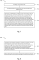
- Figure 7 is a flow chart of a method 700 for fabricating a semiconductor package.
- the method 700 may for example be used to fabricate the semiconductor package 100.
- the method 700 comprises at 701 an act of providing a semiconductor die, at 702 and act of providing a plurality of external leads, the external leads being leadframe parts, and at 703 an act of fabricating a molded body by molding over the semiconductor die and the external leads, such that the external leads are exposed from the molded body, wherein at least a first one and a second one of the plurality of external leads comprise a barb portion, the barb portion having a greater width than an innermost portion and a through hole portion of the respective external lead, the innermost portion extending from the molded body to the through hole portion, the through hole portion extending between the innermost portion and the barb portion, the through hole portion being configured to extend through a through hole of a printed circuit board, and the barb portion being configured to interlock with a surface of the printed circuit board around the through hole.
- providing the plurality of external leads comprises an act of providing a sheet metal and an act of stamping or punching the sheet metal in order to fabricate the barb portions.
- the barb portions may in particular be fabricated in the same stamping or punching process that is used to fabricate the external leads and potentially a die carrier of the semiconductor package.
- Figure 8 is a flow chart of a method 800 for fabricating a system.
- the method 800 may for example be used to fabricate the system 300.
- the method 800 comprises at 801 an act of arranging a semiconductor package (e.g. the semiconductor package 100) on a printed circuit board, such that the through hole portions of the external leads extend through respective through holes of the printed circuit board and such that the barb portions of the external leads of the semiconductor package interlock with a surface of the printed circuit board around the respective through holes to keep the semiconductor package in place on the printed circuit board.
- the method 800 may at 802 optionally comprise an act of soldering the semiconductor package to the printed circuit board.
- Example 1 is a semiconductor package, comprising: a semiconductor die, a molded body encapsulating the semiconductor die, and a plurality of external leads exposed from the molded body, the external leads being leadframe parts, wherein at least a first one and a second one of the plurality of external leads comprise a barb portion, the barb portion having a greater width than an innermost portion and a through hole portion of the respective external lead, the innermost portion extending from the molded body to the through hole portion, the through hole portion extending between the innermost portion and the barb portion, the through hole portion being configured to extend through a through hole of a printed circuit board, and the barb portion being configured to interlock with a surface of the printed circuit board around the through hole.
- Example 2 is the semiconductor package of example 1, wherein when the semiconductor package is arranged on a first side of the printed circuit board, such that the plurality of external leads extends into through holes of the printed circuit board, the barb portions are arranged on a second side of the printed circuit board, opposite the first side.
- Example 3 is the semiconductor package of example 1 or 2, wherein at least two external leads of the plurality of external leads further comprise stopper portions having a greater width than the innermost portions and the through hole portions, the stopper portions being arranged between the innermost portions and the through hole portions, and the stopper portions being configured to prevent the external leads from extending into through holes of the printed circuit board beyond the through hole portions.
- Example 4 is the semiconductor package of example 3, wherein the first one and the second one of the external leads comprise a stopper portion.
- Example 5 is the semiconductor package of one of the preceding examples, wherein the first one and the second one of the external leads are electrically insulated from the semiconductor die.
- Example 6 is the semiconductor package of one of the preceding examples, wherein the barb portion comprises a pointed end of the respective external lead.
- Example 7 is the semiconductor package of example 6, wherein the pointed end comprises a first side being a straight extension of the through hole portion and a second side being tapered with respect to the through hole portion.
- Example 8 is the semiconductor package of example 6, wherein the pointed end comprises first and second sides being tapered with respect to the through hole portion.
- Example 9 is the semiconductor package of one of the preceding examples, wherein the molded body comprises a first side configured to face the printed circuit board, an opposite second side and lateral sides connecting the first and second sides, wherein the plurality of external leads is exposed from the molded body at one or more of the lateral sides.
- Example 10 is a system, comprising: the semiconductor package of one of examples 1-9, and a printed circuit board, wherein the semiconductor package is arranged on the printed circuit board, and wherein the barb portions of the at least first one and second one of the external leads keep the semiconductor package in place on the printed circuit board.
- Example 11 is a method for fabricating a semiconductor package, the method comprising: providing a semiconductor die, providing a plurality of external leads, the external leads being leadframe parts, fabricating a molded body by molding over the semiconductor die and the external leads, such that the external leads are exposed from the molded body, wherein at least a first one and a second one of the plurality of external leads comprise a barb portion, the barb portion having a greater width than an innermost portion and a through hole portion of the respective external lead, the innermost portion extending from the molded body to the through hole portion, the through hole portion extending between the innermost portion and the barb portion, the through hole portion being configured to extend through a through hole of a printed circuit board, and the barb portion being configured to interlock with a surface of the printed circuit board around the through hole.
- Example 12 is the method of example 11, wherein providing the plurality of external leads comprises: providing a sheet metal, and stamping the sheet metal to fabricate the barb portions.
- Example 13 is a method for fabricating a system, the method comprising: arranging the semiconductor package of one of examples 1-9 on a printed circuit board, such that the through hole portions of the external leads extend through respective through holes of the printed circuit board and such that the barb portions interlock with a surface of the printed circuit board around the respective through holes to keep the semiconductor package in place on the printed circuit board.
- Example 14 is the method of example 13, further comprising: straightening a warp of the printed circuit board using the barb portions of the external leads.
- Example 15 is the method of example 13 or 14, further comprising: soldering the semiconductor package to the printed circuit board.
- Example 16 is an apparatus comprising means for performing the method according to anyone of examples 11 to 15.
Landscapes
- Engineering & Computer Science (AREA)
- Manufacturing & Machinery (AREA)
- Microelectronics & Electronic Packaging (AREA)
- Lead Frames For Integrated Circuits (AREA)
- Structures Or Materials For Encapsulating Or Coating Semiconductor Devices Or Solid State Devices (AREA)
Abstract
Description
- This disclosure relates in general to a semiconductor package comprising an external lead with a barb portion, as well as to a method of fabricating a semiconductor package comprising an external lead with a barb portion.
- Semiconductor modules or systems may comprise a semiconductor package and a printed circuit board (PCB), wherein the semiconductor package is connected to the PCB using wave soldering or selective soldering. Such modules or systems may further comprise a heatsink which may for example be arranged on the semiconductor package opposite to the PCB. Proper alignment of these components relative to each other may be impaired for example by PCB bend, package bend, shifting during transport prior to soldering or shifting during the soldering process, etc. All these factors may result in a module having misaligned components which in turn may for example increase the thermal resistance of the module. Improved semiconductor packages, improved methods for fabricating semiconductor packages, improved modules and improved methods for fabricating such modules may help in solving these and other problems.
- The problem on which the invention is based is solved by the features of the independent claims. Further advantageous examples are described in the dependent claims.
- Various aspects pertain to a semiconductor package, comprising: a semiconductor die, a molded body encapsulating the semiconductor die, and a plurality of external leads exposed from the molded body, the external leads being leadframe parts, wherein at least a first one and a second one of the plurality of external leads comprise a barb portion, the barb portion having a greater width than an innermost portion and a through hole portion of the respective external lead, the innermost portion extending from the molded body to the through hole portion, the through hole portion extending between the innermost portion and the barb portion, the through hole portion being configured to extend through a through hole of a printed circuit board, and the barb portion being configured to interlock with a surface of the printed circuit board around the through hole.
- Various aspects pertain to a method for fabricating a semiconductor package, the method comprising: providing a semiconductor die, providing a plurality of external leads, the external leads being leadframe parts, fabricating a molded body by molding over the semiconductor die and the external leads, such that the external leads are exposed from the molded body, wherein at least a first one and a second one of the plurality of external leads comprise a barb portion, the barb portion having a greater width than an innermost portion and a through hole portion of the respective external lead, the innermost portion extending from the molded body to the through hole portion, the through hole portion extending between the innermost portion and the barb portion, the through hole portion being configured to extend through a through hole of a printed circuit board, and the barb portion being configured to interlock with a surface of the printed circuit board around the through hole.
- The elements of the drawings are not necessarily to scale relative to each other. Identical reference numerals designate corresponding similar parts.
-
Figures 1A and 1B show a sectional view (Fig. 1A ) and a side view (Fig. 1B ) of a semiconductor package comprising an external lead with a barb portion. -
Figure 2 shows a detail view of an external lead with a barb portion. -
Figure 3 shows a side view of a system or module comprising a semiconductor package and a PCB. -
Figure 4 shows a perspective view of a detail of the system ofFig. 3 , according to an example. -
Figure 5 shows a perspective view of a detail of the system ofFig. 3 , according to another example. -
Figure 6 shows exemplary through holes and external leads with barb portions arranged in the through holes. -
Figure 7 is a flow chart of an exemplary method for fabricating a semiconductor package. -
Figure 8 is a flow chart of an exemplary method for fabricating a system or module. - In the following detailed description, known structures and elements are shown in schematic form in order to facilitate describing one or more aspects of the disclosure. In this regard, directional terminology, such as "top", "bottom", "left", "right", "upper", "lower" etc., is used with reference to the orientation of the Figure(s) being described. Because components of the disclosure can be positioned in a number of different orientations, the directional terminology is used for purposes of illustration only.
- In addition, while a particular feature or aspect of an example may be disclosed with respect to only one of several implementations, such feature or aspect may be combined with one or more other features or aspects of the other implementations as may be desired and advantageous for any given or particular application, unless specifically noted otherwise or unless technically restricted. Furthermore, to the extent that the terms "include", "have", "with" or other variants thereof are used in either the detailed description or the claims, such terms are intended to be inclusive in a manner similar to the term "comprise". The terms "coupled" and "connected", along with derivatives thereof may be used. It should be understood that these terms may be used to indicate that two elements cooperate or interact with each other regardless whether they are in direct physical or electrical contact, or they are not in direct contact with each other; intervening elements or layers may be provided between the "bonded", "attached", or "connected" elements. However, it is also possible that the "bonded", "attached", or "connected" elements are in direct contact with each other. Also, the term "exemplary" is merely meant as an example, rather than the best or optimal.
- An efficient semiconductor package, an efficient system and an efficient method for fabricating a semiconductor package or a system may for example reduce material consumption, ohmic losses, chemical waste, etc. and may thus enable energy and/or resource savings. Improved semiconductor packages, systems and methods for fabricating a semiconductor package or a system, as specified in this description, may thus at least indirectly contribute to green technology solutions, i.e. climate-friendly solutions providing a mitigation of energy and/or resource use.
-
Figures 1A and 1B show asemiconductor package 100 comprising asemiconductor die 110, a moldedbody 120 and a plurality ofexternal leads 130.Fig. 1A shows a sectional view andFig. 1B shows a side view along the arrow B inFig. 1A . - The semiconductor die 110 may be any suitable type of die, e.g. a MOSFET or an IGBT. The
semiconductor die 110 may be a power die configured to operate with a high voltage and/or a high electrical current. Thesemiconductor package 100 may for example comprise a plurality of semiconductor dies 110 which may be the same type of dies or different types of dies. The plurality of semiconductor dies 110 may for example be coupled to provide a circuit like an inverter circuit, a converter circuit, a half-bridge circuit, etc. Furthermore, thesemiconductor package 100 may be a power semiconductor package. - The
molded body 120 encapsulates the semiconductor die 110. The moldedbody 120 may comprise or consist of any suitable dielectric material, in particular a mold material, a polymer, a resin, etc. The moldedbody 120 may further comprise filler particles, e.g. filler particles configured to reduce the thermal resistance of the moldedbody 120. - The
external leads 130 are exposed from the moldedbody 120. According to an example, themolded body 120 comprises afirst side 121, an oppositesecond side 122 andlater sides 123 connecting the first andsecond sides external leads 130 may for example extend from at least one of thelateral sides 123. However, it is also possible that at least some of theexternal leads 130 or all of theexternal leads 130 extend from thefirst side 121 or from thesecond side 122. According to an example, thesemiconductor package 100 comprises two rows ofexternal leads 130 which extend from the moldedbody 120 on two oppositelateral sides 123, as shown inFig. 1A . - The
external leads 130 are leadframe parts. This means that during fabrication of thesemiconductor package 100, theexternal leads 130 are provided as part of a leadframe. Fabricating thesemiconductor package 100 may for example comprise punching or stamping or cutting the leadframe in order to fabricate theexternal leads 130. According to an example, theexternal leads 130 are in particular no pressfit pins. Pressfit pins would increase the costs of thesemiconductor package 100 and/or would have to be inserted into through holes with a greater expenditure of force than leadframe parts. Theexternal leads 130 may for example comprise or consist of Al or Cu. - Apart from the
external leads 130, thesemiconductor package 100 may also comprise one or more additional leadframe parts. For example, thesemiconductor package 100 may comprise one or moredie carriers 140, wherein the one ormore die carriers 140 are leadframe parts. During fabrication of thesemiconductor package 100, theexternal leads 130 and the die carrier (s) 140 may be part of the same leadframe or part of different leadframes. Furthermore, one or more of theexternal leads 130 may be integral with at least one of the die carrier(s) 140. - The semiconductor die 110 may be arranged on the
die carrier 140. Furthermore, the semiconductor die 110 may be electrically coupled to thedie carrier 140. For example, the semiconductor die 110 may comprise an electrode on a main side facing thedie carrier 140 and this electrode may be electrically coupled to thedie carrier 140 via e.g. a solder joint or a sintered joint. - As shown in
Fig. 1A , the die carrier(s) 140 may be at least partially exposed from the moldedbody 120, for example exposed from thefirst side 121 of the moldedbody 120. In this manner, a heatsink may be arranged at thefirst side 121 and no mold material is arranged between the die carrier(s) 140 and the heatsink. Alternatively, the die carrier(s) 140 are not exposed from the moldedbody 120. - The external leads 130 may for example comprise or consist of external power contacts, control contacts and/or sensor contacts of the
semiconductor package 100. According to an example, thesemiconductor package 100 comprises additional external contacts which may be different from the external leads 130. According to another example, the semiconductor package does not comprise any additional external contacts. - As shown in
Fig. 1B , at least a first one and a second one of the plurality ofexternal leads 130 comprise abarb portion 131. Thebarb portion 131 has a greater width than a throughhole portion 132 and aninnermost portion 133 of the respectiveexternal lead 130. Theinnermost portion 133 extends from the molded body to the throughhole portion 132 and the throughhole portion 132 extends between theinnermost portion 133 and thebarb portion 131. Furthermore, the throughhole portion 132 is configured to extend through a through hole of a PCB and thebarb portion 131 is configured to interlock with a surface of the PCB around the through hole. - According to an example, the
semiconductor package 100 comprises at least fourexternal leads 130 withbarb portions 131. These fourexternal leads 130 may for example be arranged at the four corners of thesemiconductor package 100. According to another example, thesemiconductor package 100 comprises at least twoexternal leads 130 with barb portions, wherein these twoexternal leads 130 are arranged at diagonally opposing corners of thesemiconductor package 100. Thesemiconductor package 100 may in general comprise any suitable number ofexternal leads 130 withbarb portions 131. It is also possible that all of theexternal leads 130 have abarb portion 131. - A single one or some or even all of the
external leads 130 with abarb portion 131 may have an electrical function as an external power contact, control contact or sensor contact of thesemiconductor package 100. However, it is also possible that one or some or even all of theexternal leads 130 with abarb portion 131 do not have an electrical function (i.e. these leads are dummy leads that are not coupled to an electrical component of thesemiconductor package 100, in particular not coupled to the semiconductor die 110). - The
barb portions 131 of individualexternal leads 130 may have different orientations. As shown inFig. 1B , the barb portions 131 (in particular, thebarb portions 131 ofexternal leads 130 on the same lateral side 123) may for example be oriented away from each other. According to another example, the barb portions 131 (in particular, thebarb portions 131 ofexternal leads 130 on the same lateral side 123) are oriented to face each other. -
Figure 2 shows a detail view of anexternal lead 130 with abarb portion 131, according to an example. A first width w1 of the barb portion may for example be about 1.5 times or 2 times or 3 times or more larger than a second width w2 of the throughhole portion 132 and theinnermost portion 131. The throughhole portion 132 and theinnermost portion 133 may for example have the same second width w2. The throughhole portion 132 and/or theinnermost portion 133 may for example have a second width w2 of 0.5mm or more, or 1mm or more, or 2mm or more, or 3mm or more, or 5mm or more. - The
barb portion 131 may comprise or consist of a pointed end of theexternal lead 130. The pointed end may for example comprise a first side being a straight extension of the throughhole portion 132 and a second side being tapered with respect to the throughhole portion 132. According to another example, the pointed end comprises first and second sides which are tapered with respect to the throughhole portion 132. The first and second sides may for example intersect with an angle of 90° or less, or 60° or less, or 45° or less. - An inner end of the
barb portion 131 may comprise anangled side 134 which may for example be arranged perpendicular to the throughhole portion 132 and/or to theinnermost portion 133. Theangled side 134 may be configured to be in direct contact with a main side of a PCB when theexternal lead 130 extends through a through hole of the PCB. In this case, theangled side 134 may essentially be parallel to the main side of the PCB. -
Figure 3 shows a side view of a system ormodule 300 comprising thesemiconductor package 100 and aPCB 310 joined to thesemiconductor package 100. ThePCB 310 may comprise afirst side 311 and an oppositesecond side 312, wherein thesemiconductor package 100 is arranged at thefirst side 311. - As shown in
Fig. 3 , thePCB 310 comprises a plurality of throughholes 320, wherein theexternal leads 130 extend into or even completely through the throughholes 320. Thebarb portions 131 are arranged at thesecond side 312 of thePCB 310 and the throughhole portions 132 are arranged within the throughholes 320. - The
second side 122 of the moldedbody 120 may be in direct contact with thefirst side 311 of thePCB 310. However, it is also possible that the moldedbody 120 and thePCB 310 are not in direct contact. - Fabricating the
system 300 may comprise arranging thePCB 310 on thesemiconductor package 100 such that the external leads are arranged in the throughholes 320 and then soldering thePCB 310 to thesemiconductor package 100. - Once the
PCB 310 is arranged on thesemiconductor package 100, thebarb portions 131 may help in keeping thePCB 310 in place. In particular, thebarb portions 131 prevent thePCB 310 from shifting out of position during transport, during soldering, etc. - Furthermore, the
barb portions 131 may for example help in countering a potential warpage of thePCB 310 and/or a warpage of thesemiconductor package 100. By pulling thePCB 310 into shape using thebarb portions 131, a warpage may be remedied. This in turn may help in improving a thermal connection between thesemiconductor package 100 and a heatsink arranged on thefirst side 121 of the moldedbody 120. By eliminating or at least reducing PCB warpage or package warpage, the alignment of the semiconductor package relative to the heatsink may be improved which may reduce the required minimum thickness of a layer of thermal interface material (TIM) between thesemiconductor package 100 and the heatsink. - As shown in
Fig. 3 ,barbed leads 130 may be longer than the non-barbed leads 130. - As shown in
Fig. 3 , thesystem 300 may comprise aheatsink 330 arranged at thefirst side 121 of the moldedbody 120. Anintervening layer 340 e.g. comprising or consisting of TIM may be arranged between the moldedbody 120 and theheatsink 330. Since the relative positions of thesemiconductor package 100 and thePCB 310 are fixed by theexternal leads 130 withbarb portions 131, the no misalignment or almost no misalignment of these parts has to be accounted for during fabrication. For this reason, the interveninglayer 340 may be thinner than it would have to be in the case that misalignments would have to be accounted for. This in turn reduces the thermal resistance between thesemiconductor package 100 and theheatsink 330. -
Figure 4 shows a perspective view of a detail of thesystem 300, according to a further example.Figure 4 in particular shows theexternal leads 130 arranged within the throughholes 320 of thePCB 310 in greater detail. - As shown in
Fig. 4 , at least one of theexternal leads 130 may comprise astopper portion 135. Thestopper portion 135 has a larger width than theinnermost portion 133 and the throughhole portion 132 of thatexternal lead 130. Thestopper portion 135 is arranged between theinnermost portion 133 and the throughhole portion 132 of the respective external lead(s) 130. Furthermore, thestopper portion 135 is configured to prevent theexternal lead 130 from extending into throughhole 320 of thePCB 310 beyond the throughhole portion 132. - A width of the
stopper portion 135 may for example be about two times or more, about three times or more, about four times or more, or about five times or more than the second width w2. The width of thestopper portion 135 may for example be about the same as the first width w1 or larger than w1. - The
stopper portion 135 may essentially have a T-shape or any other suitable shape. Thestopper portion 135 may have an angled side which may be configured to be in direct contact with thefirst side 311 of thePCB 310. The width of thestopper portion 135 may in particular be larger than a diameter of the throughhole 320. - According to an example, at least four of the
external leads 130 of thesemiconductor package 100 comprise astopper portion 135. The fourexternal leads 130 withstopper portions 135 may e.g. be arranged at the four corners of thesemiconductor package 100. According to an example, all of theexternal leads 130 comprise astopper portion 135. - The
stopper portions 135 may for example be configured to provide a defined distance between thefirst side 311 of thePCB 310 and thesecond side 122 of the moldedbody 120. In other words, there may be a nonzero gap between thefirst side 311 and thesecond side 122. -
Figure 5 shows a perspective view of a detail of thesystem 300 according to another example. In the example shown inFig. 5 , anexternal lead 130 comprises both thebarb portion 131 and thestopper portion 135. In the example shown inFig. 4 on the other hand, an external lead with abarb portion 131 does not comprise astopper portion 135 and vice versa. - Furthermore, the
barb portion 135 of the example ofFig. 5 comprises a pointed end, wherein the pointed end is provided by first and second sides of thebarb portion 135 which are tapered with respect to the throughhole portion 132. Thebarb portion 135 of the example ofFig. 4 on the other hand comprises a pointed end, wherein a first side of the barb portion 135 a straight extension of the throughhole portion 132 and a second side of thebarb portion 135 is tapered with respect to the throughhole portion 132. -
Figure 6 shows different examples of through holes 320_1 to 320_3 which may be used in thesystem 300.Fig. 6 also shows anexternal lead 130 with abarb portion 131 arranged within each of the through holes 320_1 to 320 3. The top row ofFig. 6 shows a plan view of the through holes 320_1 to 320_3 and the bottom row ofFig. 6 shows a sectional view. - The through hole 320_1 comprises an essentially elongated shape, wherein the longer side may for example be as long or longer than the first width w1 of the
barb portion 131. The through hole 320_2 comprises an essentially round shape, wherein a diameter of the through hole 320_2 may for example be as larger or larger than the first width w1. The through hole 320_3 comprises an essentially conical cross section, wherein at least the larger end of the conus may have a diameter that is as large or larger than w1. - As shown in
Fig. 6 , a central axis of the through holes 320_1 to 320_3 may be shifted with respect to a central axis of theexternal lead 130 such that thebarb portion 131 can hook into thePCB 310. - According to an example, the elongated through hole 320_1 or the through hole 320_2 with the large diameter may also have the conical cross section of the through hole 320_3.
-
Figure 7 is a flow chart of amethod 700 for fabricating a semiconductor package. Themethod 700 may for example be used to fabricate thesemiconductor package 100. - The
method 700 comprises at 701 an act of providing a semiconductor die, at 702 and act of providing a plurality of external leads, the external leads being leadframe parts, and at 703 an act of fabricating a molded body by molding over the semiconductor die and the external leads, such that the external leads are exposed from the molded body, wherein at least a first one and a second one of the plurality of external leads comprise a barb portion, the barb portion having a greater width than an innermost portion and a through hole portion of the respective external lead, the innermost portion extending from the molded body to the through hole portion, the through hole portion extending between the innermost portion and the barb portion, the through hole portion being configured to extend through a through hole of a printed circuit board, and the barb portion being configured to interlock with a surface of the printed circuit board around the through hole. - According to an example of the
method 700, providing the plurality of external leads comprises an act of providing a sheet metal and an act of stamping or punching the sheet metal in order to fabricate the barb portions. The barb portions may in particular be fabricated in the same stamping or punching process that is used to fabricate the external leads and potentially a die carrier of the semiconductor package. -
Figure 8 is a flow chart of amethod 800 for fabricating a system. Themethod 800 may for example be used to fabricate thesystem 300. - The
method 800 comprises at 801 an act of arranging a semiconductor package (e.g. the semiconductor package 100) on a printed circuit board, such that the through hole portions of the external leads extend through respective through holes of the printed circuit board and such that the barb portions of the external leads of the semiconductor package interlock with a surface of the printed circuit board around the respective through holes to keep the semiconductor package in place on the printed circuit board. Themethod 800 may at 802 optionally comprise an act of soldering the semiconductor package to the printed circuit board. - In the following, the semiconductor package, the system, the method for fabricating a semiconductor package and the method for fabricating a system are further explained using specific examples.
- Example 1 is a semiconductor package, comprising: a semiconductor die, a molded body encapsulating the semiconductor die, and a plurality of external leads exposed from the molded body, the external leads being leadframe parts, wherein at least a first one and a second one of the plurality of external leads comprise a barb portion, the barb portion having a greater width than an innermost portion and a through hole portion of the respective external lead, the innermost portion extending from the molded body to the through hole portion, the through hole portion extending between the innermost portion and the barb portion, the through hole portion being configured to extend through a through hole of a printed circuit board, and the barb portion being configured to interlock with a surface of the printed circuit board around the through hole.
- Example 2 is the semiconductor package of example 1, wherein when the semiconductor package is arranged on a first side of the printed circuit board, such that the plurality of external leads extends into through holes of the printed circuit board, the barb portions are arranged on a second side of the printed circuit board, opposite the first side.
- Example 3 is the semiconductor package of example 1 or 2, wherein at least two external leads of the plurality of external leads further comprise stopper portions having a greater width than the innermost portions and the through hole portions, the stopper portions being arranged between the innermost portions and the through hole portions, and the stopper portions being configured to prevent the external leads from extending into through holes of the printed circuit board beyond the through hole portions.
- Example 4 is the semiconductor package of example 3, wherein the first one and the second one of the external leads comprise a stopper portion.
- Example 5 is the semiconductor package of one of the preceding examples, wherein the first one and the second one of the external leads are electrically insulated from the semiconductor die.
- Example 6 is the semiconductor package of one of the preceding examples, wherein the barb portion comprises a pointed end of the respective external lead.
- Example 7 is the semiconductor package of example 6, wherein the pointed end comprises a first side being a straight extension of the through hole portion and a second side being tapered with respect to the through hole portion.
- Example 8 is the semiconductor package of example 6, wherein the pointed end comprises first and second sides being tapered with respect to the through hole portion.
- Example 9 is the semiconductor package of one of the preceding examples, wherein the molded body comprises a first side configured to face the printed circuit board, an opposite second side and lateral sides connecting the first and second sides, wherein the plurality of external leads is exposed from the molded body at one or more of the lateral sides.
- Example 10 is a system, comprising: the semiconductor package of one of examples 1-9, and a printed circuit board, wherein the semiconductor package is arranged on the printed circuit board, and wherein the barb portions of the at least first one and second one of the external leads keep the semiconductor package in place on the printed circuit board.
- Example 11 is a method for fabricating a semiconductor package, the method comprising: providing a semiconductor die, providing a plurality of external leads, the external leads being leadframe parts, fabricating a molded body by molding over the semiconductor die and the external leads, such that the external leads are exposed from the molded body, wherein at least a first one and a second one of the plurality of external leads comprise a barb portion, the barb portion having a greater width than an innermost portion and a through hole portion of the respective external lead, the innermost portion extending from the molded body to the through hole portion, the through hole portion extending between the innermost portion and the barb portion, the through hole portion being configured to extend through a through hole of a printed circuit board, and the barb portion being configured to interlock with a surface of the printed circuit board around the through hole.
- Example 12 is the method of example 11, wherein providing the plurality of external leads comprises: providing a sheet metal, and stamping the sheet metal to fabricate the barb portions.
- Example 13 is a method for fabricating a system, the method comprising: arranging the semiconductor package of one of examples 1-9 on a printed circuit board, such that the through hole portions of the external leads extend through respective through holes of the printed circuit board and such that the barb portions interlock with a surface of the printed circuit board around the respective through holes to keep the semiconductor package in place on the printed circuit board.
- Example 14 is the method of example 13, further comprising: straightening a warp of the printed circuit board using the barb portions of the external leads.
- Example 15 is the method of example 13 or 14, further comprising: soldering the semiconductor package to the printed circuit board.
- Example 16 is an apparatus comprising means for performing the method according to anyone of examples 11 to 15.
- While the disclosure has been illustrated and described with respect to one or more implementations, alterations and/or modifications may be made to the illustrated examples without departing from the spirit and scope of the appended claims. In particular regard to the various functions performed by the above described components or structures (assemblies, devices, circuits, systems, etc.), the terms (including a reference to a "means") used to describe such components are intended to correspond, unless otherwise indicated, to any component or structure which performs the specified function of the described component (e.g., that is functionally equivalent), even though not structurally equivalent to the disclosed structure which performs the function in the herein illustrated exemplary implementations of the disclosure.
Claims (15)
- A semiconductor package (100), comprising:a semiconductor die (110),a molded body (120) encapsulating the semiconductor die (110), anda plurality of external leads (130) exposed from the molded body (120), the external leads (130) being leadframe parts,wherein at least a first one and a second one of the plurality of external leads (130) comprise a barb portion (131), the barb portion (131) having a greater width than an innermost portion (133) and a through hole (132) portion of the respective external lead (130),the innermost portion (133) extending from the molded body (120) to the through hole portion (132),the through hole portion (132) extending between the innermost portion (133) and the barb portion (131),the through hole portion (132) being configured to extend through a through hole of a printed circuit board, andthe barb portion (131) being configured to interlock with a surface of the printed circuit board around the through hole.
- The semiconductor package (100) of claim 1, wherein when the semiconductor package (100) is arranged on a first side of the printed circuit board, such that the plurality of external leads (130) extends into through holes of the printed circuit board, the barb portions (131) are arranged on a second side of the printed circuit board, opposite the first side.
- The semiconductor package (100) of claim 1 or 2, wherein at least two external leads (130) of the plurality of external leads (130) further comprise stopper portions (135) having a greater width than the innermost portions (133) and the through hole portions (132),the stopper portions (135) being arranged between the innermost portions (133) and the through hole portions (132), andthe stopper portions (135) being configured to prevent the external leads (130) from extending into through holes of the printed circuit board beyond the through hole portions (132) .
- The semiconductor package (100) of claim 3, wherein the first one and the second one of the external leads (130) comprise a stopper portion (135).
- The semiconductor package (100) of one of the preceding claims, wherein the first one and the second one of the external leads (130) are electrically insulated from the semiconductor die (110).
- The semiconductor package (100) of one of the preceding claims, wherein the barb portion (131) comprises a pointed end of the respective external lead (130).
- The semiconductor package (100) of claim 6, wherein the pointed end comprises a first side being a straight extension of the through hole portion (132) and a second side being tapered with respect to the through hole portion (132).
- The semiconductor package (100) of claim 6, wherein the pointed end comprises first and second sides being tapered with respect to the through hole portion (132).
- The semiconductor package (100) of one of the preceding claims, wherein the molded body (120) comprises a first side (121) configured to face the printed circuit board, an opposite second side (122) and lateral sides (123) connecting the first and second sides,
wherein the plurality of external leads (130) is exposed from the molded body (120) at one or more of the lateral sides (123). - A system (300), comprising:the semiconductor package (100) of one of claims 1-9, anda printed circuit board (310),wherein the semiconductor package (110) is arranged on the printed circuit board (310), andwherein the barb portions (131) of the at least first one and second one of the external leads (130) keep the semiconductor package (100) in place on the printed circuit board (310) .
- A method (700) for fabricating a semiconductor package, the method comprising:providing (701) a semiconductor die,providing (702) a plurality of external leads, the external leads being leadframe parts,fabricating (703) a molded body by molding over the semiconductor die and the external leads, such that the external leads are exposed from the molded body,wherein at least a first one and a second one of the plurality of external leads comprise a barb portion, the barb portion having a greater width than an innermost portion and a through hole portion of the respective external lead,the innermost portion extending from the molded body to the through hole portion,the through hole portion extending between the innermost portion and the barb portion,the through hole portion being configured to extend through a through hole of a printed circuit board, andthe barb portion being configured to interlock with a surface of the printed circuit board around the through hole.
- The method (700) of claim 11, wherein providing (702) the plurality of external leads comprises:providing a sheet metal, andstamping the sheet metal to fabricate the barb portions.
- A method (800) for fabricating a system, the method comprising:
arranging (801) the semiconductor package of one of claims 1-9 on a printed circuit board, such that the through hole portions of the external leads extend through respective through holes of the printed circuit board and such that the barb portions interlock with a surface of the printed circuit board around the respective through holes to keep the semiconductor package in place on the printed circuit board. - The method (800) of claim 13, further comprising:
straightening a warp of the printed circuit board using the barb portions of the external leads. - The method (800) of claim 13 or 14, further comprising:
soldering (802) the semiconductor package to the printed circuit board.
Priority Applications (1)
| Application Number | Priority Date | Filing Date | Title |
|---|---|---|---|
| EP22167633.1A EP4261881B1 (en) | 2022-04-11 | 2022-04-11 | Semiconductor package comprising an external lead with a barb portion |
Applications Claiming Priority (1)
| Application Number | Priority Date | Filing Date | Title |
|---|---|---|---|
| EP22167633.1A EP4261881B1 (en) | 2022-04-11 | 2022-04-11 | Semiconductor package comprising an external lead with a barb portion |
Publications (2)
| Publication Number | Publication Date |
|---|---|
| EP4261881A1 true EP4261881A1 (en) | 2023-10-18 |
| EP4261881B1 EP4261881B1 (en) | 2025-12-24 |
Family
ID=81307106
Family Applications (1)
| Application Number | Title | Priority Date | Filing Date |
|---|---|---|---|
| EP22167633.1A Active EP4261881B1 (en) | 2022-04-11 | 2022-04-11 | Semiconductor package comprising an external lead with a barb portion |
Country Status (1)
| Country | Link |
|---|---|
| EP (1) | EP4261881B1 (en) |
Citations (3)
| Publication number | Priority date | Publication date | Assignee | Title |
|---|---|---|---|---|
| JPH01235360A (en) * | 1988-03-16 | 1989-09-20 | Ricoh Co Ltd | Semiconductor integrated circuit device |
| JPH03255654A (en) * | 1990-03-05 | 1991-11-14 | Nec Corp | Surface mounting semiconductor device |
| JP2003007380A (en) * | 2001-06-19 | 2003-01-10 | Microjenics Inc | Electronic components |
-
2022
- 2022-04-11 EP EP22167633.1A patent/EP4261881B1/en active Active
Patent Citations (3)
| Publication number | Priority date | Publication date | Assignee | Title |
|---|---|---|---|---|
| JPH01235360A (en) * | 1988-03-16 | 1989-09-20 | Ricoh Co Ltd | Semiconductor integrated circuit device |
| JPH03255654A (en) * | 1990-03-05 | 1991-11-14 | Nec Corp | Surface mounting semiconductor device |
| JP2003007380A (en) * | 2001-06-19 | 2003-01-10 | Microjenics Inc | Electronic components |
Also Published As
| Publication number | Publication date |
|---|---|
| EP4261881B1 (en) | 2025-12-24 |
Similar Documents
| Publication | Publication Date | Title |
|---|---|---|
| JP5241177B2 (en) | Semiconductor device and manufacturing method of semiconductor device | |
| DE69535712T2 (en) | Method for producing a semiconductor chip carrier | |
| KR100390094B1 (en) | Semiconductor device and manufacturing method | |
| US9437460B2 (en) | Method for manufacturing semiconductor device | |
| US6580161B2 (en) | Semiconductor device and method of making the same | |
| CN108695177B (en) | Semiconductor device and method of manufacturing the same | |
| US6114189A (en) | Molded array integrated circuit package | |
| DE112012003296B4 (en) | Semiconductor module and semiconductor device with the semiconductor module | |
| KR102011559B1 (en) | Semiconductor device and manufacturing method thereof | |
| CN101131938A (en) | Stamped leadframe and method of making same | |
| US20150076674A1 (en) | Semiconductor device and method of manufacturing the same | |
| US20210313294A1 (en) | Semiconductor package and method for fabricating the same | |
| US20170365547A1 (en) | Semiconductor device, manufacturing method, and conductive post | |
| US20230411254A1 (en) | Molded power semiconductor package with gate connector feature | |
| US20240087995A1 (en) | Power semiconductor package and method for fabricating the same | |
| JP2013021371A (en) | Semiconductor device and semiconductor device manufacturing method | |
| US20200373231A1 (en) | Semiconductor package with guide pin | |
| DE102021125094A1 (en) | SEMICONDUCTOR PACKAGE WITH A CHIP CARRIAGE WITH A PAD OFFSET FEATURE | |
| DE102023122872B3 (en) | POWER ELECTRONICS SYSTEM COMPRISING A POWER SEMICONDUCTOR MODULE AND A CURRENT SENSOR AND A POWER SEMICONDUCTOR MODULE | |
| DE102017129563B4 (en) | SEMICONDUCTOR DEVICES WITH EXPOSED OPPOSITE CHIP PADS AND METHOD OF MANUFACTURE THEREOF | |
| CN210296358U (en) | Packaging frame of power module, packaging frame array and packaging body | |
| DE112020007426T5 (en) | SEMICONDUCTOR DEVICE AND POWER CONVERTER DEVICE | |
| EP4261881B1 (en) | Semiconductor package comprising an external lead with a barb portion | |
| JP5826234B2 (en) | Semiconductor device and manufacturing method of semiconductor device | |
| JP4881256B2 (en) | Power semiconductor module |
Legal Events
| Date | Code | Title | Description |
|---|---|---|---|
| PUAI | Public reference made under article 153(3) epc to a published international application that has entered the european phase |
Free format text: ORIGINAL CODE: 0009012 |
|
| STAA | Information on the status of an ep patent application or granted ep patent |
Free format text: STATUS: THE APPLICATION HAS BEEN PUBLISHED |
|
| AK | Designated contracting states |
Kind code of ref document: A1 Designated state(s): AL AT BE BG CH CY CZ DE DK EE ES FI FR GB GR HR HU IE IS IT LI LT LU LV MC MK MT NL NO PL PT RO RS SE SI SK SM TR |
|
| STAA | Information on the status of an ep patent application or granted ep patent |
Free format text: STATUS: REQUEST FOR EXAMINATION WAS MADE |
|
| 17P | Request for examination filed |
Effective date: 20231108 |
|
| RBV | Designated contracting states (corrected) |
Designated state(s): AL AT BE BG CH CY CZ DE DK EE ES FI FR GB GR HR HU IE IS IT LI LT LU LV MC MK MT NL NO PL PT RO RS SE SI SK SM TR |
|
| GRAP | Despatch of communication of intention to grant a patent |
Free format text: ORIGINAL CODE: EPIDOSNIGR1 |
|
| STAA | Information on the status of an ep patent application or granted ep patent |
Free format text: STATUS: GRANT OF PATENT IS INTENDED |
|
| RIC1 | Information provided on ipc code assigned before grant |
Ipc: H01L 23/495 20060101AFI20250715BHEP Ipc: H05K 3/32 20060101ALI20250715BHEP Ipc: H05K 3/30 20060101ALI20250715BHEP |
|
| INTG | Intention to grant announced |
Effective date: 20250724 |
|
| GRAS | Grant fee paid |
Free format text: ORIGINAL CODE: EPIDOSNIGR3 |
|
| GRAA | (expected) grant |
Free format text: ORIGINAL CODE: 0009210 |
|
| STAA | Information on the status of an ep patent application or granted ep patent |
Free format text: STATUS: THE PATENT HAS BEEN GRANTED |
|
| REG | Reference to a national code |
Ref country code: DE Ref legal event code: R079 Ref document number: 602022027276 Country of ref document: DE Free format text: PREVIOUS MAIN CLASS: H01L0023495000 Ipc: H10W0070400000 |
|
| AK | Designated contracting states |
Kind code of ref document: B1 Designated state(s): AL AT BE BG CH CY CZ DE DK EE ES FI FR GB GR HR HU IE IS IT LI LT LU LV MC MK MT NL NO PL PT RO RS SE SI SK SM TR |
|
| REG | Reference to a national code |
Ref country code: CH Ref legal event code: F10 Free format text: ST27 STATUS EVENT CODE: U-0-0-F10-F00 (AS PROVIDED BY THE NATIONAL OFFICE) Effective date: 20251224 Ref country code: GB Ref legal event code: FG4D |
|
| REG | Reference to a national code |
Ref country code: DE Ref legal event code: R096 Ref document number: 602022027276 Country of ref document: DE |
|
| P01 | Opt-out of the competence of the unified patent court (upc) registered |
Free format text: CASE NUMBER: UPC_APP_0002207_4261881/2026 Effective date: 20260121 |
|
| REG | Reference to a national code |
Ref country code: LT Ref legal event code: MG9D |
|
| PG25 | Lapsed in a contracting state [announced via postgrant information from national office to epo] |
Ref country code: NO Free format text: LAPSE BECAUSE OF FAILURE TO SUBMIT A TRANSLATION OF THE DESCRIPTION OR TO PAY THE FEE WITHIN THE PRESCRIBED TIME-LIMIT Effective date: 20260324 |
|
| PG25 | Lapsed in a contracting state [announced via postgrant information from national office to epo] |
Ref country code: FI Free format text: LAPSE BECAUSE OF FAILURE TO SUBMIT A TRANSLATION OF THE DESCRIPTION OR TO PAY THE FEE WITHIN THE PRESCRIBED TIME-LIMIT Effective date: 20251224 Ref country code: HR Free format text: LAPSE BECAUSE OF FAILURE TO SUBMIT A TRANSLATION OF THE DESCRIPTION OR TO PAY THE FEE WITHIN THE PRESCRIBED TIME-LIMIT Effective date: 20251224 |
|
| PG25 | Lapsed in a contracting state [announced via postgrant information from national office to epo] |
Ref country code: RS Free format text: LAPSE BECAUSE OF FAILURE TO SUBMIT A TRANSLATION OF THE DESCRIPTION OR TO PAY THE FEE WITHIN THE PRESCRIBED TIME-LIMIT Effective date: 20260324 |
|
| PG25 | Lapsed in a contracting state [announced via postgrant information from national office to epo] |
Ref country code: LV Free format text: LAPSE BECAUSE OF FAILURE TO SUBMIT A TRANSLATION OF THE DESCRIPTION OR TO PAY THE FEE WITHIN THE PRESCRIBED TIME-LIMIT Effective date: 20251224 |
|
| REG | Reference to a national code |
Ref country code: NL Ref legal event code: MP Effective date: 20251224 |
|
| PG25 | Lapsed in a contracting state [announced via postgrant information from national office to epo] |
Ref country code: BG Free format text: LAPSE BECAUSE OF FAILURE TO SUBMIT A TRANSLATION OF THE DESCRIPTION OR TO PAY THE FEE WITHIN THE PRESCRIBED TIME-LIMIT Effective date: 20251224 |
|
| REG | Reference to a national code |
Ref country code: AT Ref legal event code: MK05 Ref document number: 1871630 Country of ref document: AT Kind code of ref document: T Effective date: 20251224 |
|
| PG25 | Lapsed in a contracting state [announced via postgrant information from national office to epo] |
Ref country code: NL Free format text: LAPSE BECAUSE OF FAILURE TO SUBMIT A TRANSLATION OF THE DESCRIPTION OR TO PAY THE FEE WITHIN THE PRESCRIBED TIME-LIMIT Effective date: 20251224 |
|
| PG25 | Lapsed in a contracting state [announced via postgrant information from national office to epo] |
Ref country code: LT Free format text: LAPSE BECAUSE OF FAILURE TO SUBMIT A TRANSLATION OF THE DESCRIPTION OR TO PAY THE FEE WITHIN THE PRESCRIBED TIME-LIMIT Effective date: 20251224 |
|
| PG25 | Lapsed in a contracting state [announced via postgrant information from national office to epo] |
Ref country code: SM Free format text: LAPSE BECAUSE OF FAILURE TO SUBMIT A TRANSLATION OF THE DESCRIPTION OR TO PAY THE FEE WITHIN THE PRESCRIBED TIME-LIMIT Effective date: 20251224 |
|
| PG25 | Lapsed in a contracting state [announced via postgrant information from national office to epo] |
Ref country code: ES Free format text: LAPSE BECAUSE OF FAILURE TO SUBMIT A TRANSLATION OF THE DESCRIPTION OR TO PAY THE FEE WITHIN THE PRESCRIBED TIME-LIMIT Effective date: 20251224 |
|
| PG25 | Lapsed in a contracting state [announced via postgrant information from national office to epo] |
Ref country code: PL Free format text: LAPSE BECAUSE OF FAILURE TO SUBMIT A TRANSLATION OF THE DESCRIPTION OR TO PAY THE FEE WITHIN THE PRESCRIBED TIME-LIMIT Effective date: 20251224 |
|
| PG25 | Lapsed in a contracting state [announced via postgrant information from national office to epo] |
Ref country code: IT Free format text: LAPSE BECAUSE OF FAILURE TO SUBMIT A TRANSLATION OF THE DESCRIPTION OR TO PAY THE FEE WITHIN THE PRESCRIBED TIME-LIMIT Effective date: 20251224 |
|
| PG25 | Lapsed in a contracting state [announced via postgrant information from national office to epo] |
Ref country code: AT Free format text: LAPSE BECAUSE OF FAILURE TO SUBMIT A TRANSLATION OF THE DESCRIPTION OR TO PAY THE FEE WITHIN THE PRESCRIBED TIME-LIMIT Effective date: 20251224 |
|
| PG25 | Lapsed in a contracting state [announced via postgrant information from national office to epo] |
Ref country code: EE Free format text: LAPSE BECAUSE OF FAILURE TO SUBMIT A TRANSLATION OF THE DESCRIPTION OR TO PAY THE FEE WITHIN THE PRESCRIBED TIME-LIMIT Effective date: 20251224 |
|
| PG25 | Lapsed in a contracting state [announced via postgrant information from national office to epo] |
Ref country code: IS Free format text: LAPSE BECAUSE OF FAILURE TO SUBMIT A TRANSLATION OF THE DESCRIPTION OR TO PAY THE FEE WITHIN THE PRESCRIBED TIME-LIMIT Effective date: 20260424 Ref country code: PT Free format text: LAPSE BECAUSE OF FAILURE TO SUBMIT A TRANSLATION OF THE DESCRIPTION OR TO PAY THE FEE WITHIN THE PRESCRIBED TIME-LIMIT Effective date: 20260424 |
|
| PG25 | Lapsed in a contracting state [announced via postgrant information from national office to epo] |
Ref country code: CZ Free format text: LAPSE BECAUSE OF FAILURE TO SUBMIT A TRANSLATION OF THE DESCRIPTION OR TO PAY THE FEE WITHIN THE PRESCRIBED TIME-LIMIT Effective date: 20251224 |
|
| PG25 | Lapsed in a contracting state [announced via postgrant information from national office to epo] |
Ref country code: SK Free format text: LAPSE BECAUSE OF FAILURE TO SUBMIT A TRANSLATION OF THE DESCRIPTION OR TO PAY THE FEE WITHIN THE PRESCRIBED TIME-LIMIT Effective date: 20251224 |
|
| PG25 | Lapsed in a contracting state [announced via postgrant information from national office to epo] |
Ref country code: SE Free format text: LAPSE BECAUSE OF FAILURE TO SUBMIT A TRANSLATION OF THE DESCRIPTION OR TO PAY THE FEE WITHIN THE PRESCRIBED TIME-LIMIT Effective date: 20251224 |