EP4258839A1 - Method for fabricating semiconductor structure and semiconductor structure - Google Patents
Method for fabricating semiconductor structure and semiconductor structure Download PDFInfo
- Publication number
- EP4258839A1 EP4258839A1 EP21950753.0A EP21950753A EP4258839A1 EP 4258839 A1 EP4258839 A1 EP 4258839A1 EP 21950753 A EP21950753 A EP 21950753A EP 4258839 A1 EP4258839 A1 EP 4258839A1
- Authority
- EP
- European Patent Office
- Prior art keywords
- conductive pillar
- semiconductor structure
- top surface
- area
- upper conductive
- Prior art date
- Legal status (The legal status is an assumption and is not a legal conclusion. Google has not performed a legal analysis and makes no representation as to the accuracy of the status listed.)
- Pending
Links
Images


Classifications
-
- H—ELECTRICITY
- H10—SEMICONDUCTOR DEVICES; ELECTRIC SOLID-STATE DEVICES NOT OTHERWISE PROVIDED FOR
- H10W—GENERIC PACKAGES, INTERCONNECTIONS, CONNECTORS OR OTHER CONSTRUCTIONAL DETAILS OF DEVICES COVERED BY CLASS H10
- H10W10/00—Isolation regions in semiconductor bodies between components of integrated devices
- H10W10/10—Isolation regions comprising dielectric materials
- H10W10/13—Isolation regions comprising dielectric materials formed using local oxidation of silicon [LOCOS], e.g. sealed interface localised oxidation [SILO] or side-wall mask isolation [SWAMI]
-
- H—ELECTRICITY
- H10—SEMICONDUCTOR DEVICES; ELECTRIC SOLID-STATE DEVICES NOT OTHERWISE PROVIDED FOR
- H10W—GENERIC PACKAGES, INTERCONNECTIONS, CONNECTORS OR OTHER CONSTRUCTIONAL DETAILS OF DEVICES COVERED BY CLASS H10
- H10W20/00—Interconnections in chips, wafers or substrates
- H10W20/40—Interconnections external to wafers or substrates, e.g. back-end-of-line [BEOL] metallisations or vias connecting to gate electrodes
-
- H—ELECTRICITY
- H10—SEMICONDUCTOR DEVICES; ELECTRIC SOLID-STATE DEVICES NOT OTHERWISE PROVIDED FOR
- H10B—ELECTRONIC MEMORY DEVICES
- H10B12/00—Dynamic random access memory [DRAM] devices
-
- H—ELECTRICITY
- H10—SEMICONDUCTOR DEVICES; ELECTRIC SOLID-STATE DEVICES NOT OTHERWISE PROVIDED FOR
- H10B—ELECTRONIC MEMORY DEVICES
- H10B12/00—Dynamic random access memory [DRAM] devices
- H10B12/30—DRAM devices comprising one-transistor - one-capacitor [1T-1C] memory cells
-
- H—ELECTRICITY
- H10—SEMICONDUCTOR DEVICES; ELECTRIC SOLID-STATE DEVICES NOT OTHERWISE PROVIDED FOR
- H10B—ELECTRONIC MEMORY DEVICES
- H10B12/00—Dynamic random access memory [DRAM] devices
- H10B12/30—DRAM devices comprising one-transistor - one-capacitor [1T-1C] memory cells
- H10B12/48—Data lines or contacts therefor
-
- H—ELECTRICITY
- H10—SEMICONDUCTOR DEVICES; ELECTRIC SOLID-STATE DEVICES NOT OTHERWISE PROVIDED FOR
- H10B—ELECTRONIC MEMORY DEVICES
- H10B12/00—Dynamic random access memory [DRAM] devices
- H10B12/50—Peripheral circuit region structures
-
- H—ELECTRICITY
- H10—SEMICONDUCTOR DEVICES; ELECTRIC SOLID-STATE DEVICES NOT OTHERWISE PROVIDED FOR
- H10P—GENERIC PROCESSES OR APPARATUS FOR THE MANUFACTURE OR TREATMENT OF DEVICES COVERED BY CLASS H10
- H10P50/00—Etching of wafers, substrates or parts of devices
- H10P50/20—Dry etching; Plasma etching; Reactive-ion etching
-
- H—ELECTRICITY
- H10—SEMICONDUCTOR DEVICES; ELECTRIC SOLID-STATE DEVICES NOT OTHERWISE PROVIDED FOR
- H10P—GENERIC PROCESSES OR APPARATUS FOR THE MANUFACTURE OR TREATMENT OF DEVICES COVERED BY CLASS H10
- H10P52/00—Grinding, lapping or polishing of wafers, substrates or parts of devices
-
- H—ELECTRICITY
- H10—SEMICONDUCTOR DEVICES; ELECTRIC SOLID-STATE DEVICES NOT OTHERWISE PROVIDED FOR
- H10P—GENERIC PROCESSES OR APPARATUS FOR THE MANUFACTURE OR TREATMENT OF DEVICES COVERED BY CLASS H10
- H10P95/00—Generic processes or apparatus for manufacture or treatments not covered by the other groups of this subclass
- H10P95/70—Chemical treatments
-
- H—ELECTRICITY
- H10—SEMICONDUCTOR DEVICES; ELECTRIC SOLID-STATE DEVICES NOT OTHERWISE PROVIDED FOR
- H10W—GENERIC PACKAGES, INTERCONNECTIONS, CONNECTORS OR OTHER CONSTRUCTIONAL DETAILS OF DEVICES COVERED BY CLASS H10
- H10W10/00—Isolation regions in semiconductor bodies between components of integrated devices
- H10W10/01—Manufacture or treatment
- H10W10/011—Manufacture or treatment of isolation regions comprising dielectric materials
- H10W10/012—Manufacture or treatment of isolation regions comprising dielectric materials using local oxidation of silicon [LOCOS]
- H10W10/0121—Manufacture or treatment of isolation regions comprising dielectric materials using local oxidation of silicon [LOCOS] in regions recessed from the surface, e.g. in trenches or grooves
- H10W10/0123—Manufacture or treatment of isolation regions comprising dielectric materials using local oxidation of silicon [LOCOS] in regions recessed from the surface, e.g. in trenches or grooves using auxiliary pillars in the regions
-
- H—ELECTRICITY
- H10—SEMICONDUCTOR DEVICES; ELECTRIC SOLID-STATE DEVICES NOT OTHERWISE PROVIDED FOR
- H10W—GENERIC PACKAGES, INTERCONNECTIONS, CONNECTORS OR OTHER CONSTRUCTIONAL DETAILS OF DEVICES COVERED BY CLASS H10
- H10W10/00—Isolation regions in semiconductor bodies between components of integrated devices
- H10W10/01—Manufacture or treatment
- H10W10/011—Manufacture or treatment of isolation regions comprising dielectric materials
- H10W10/014—Manufacture or treatment of isolation regions comprising dielectric materials using trench refilling with dielectric materials, e.g. shallow trench isolations
-
- H—ELECTRICITY
- H10—SEMICONDUCTOR DEVICES; ELECTRIC SOLID-STATE DEVICES NOT OTHERWISE PROVIDED FOR
- H10W—GENERIC PACKAGES, INTERCONNECTIONS, CONNECTORS OR OTHER CONSTRUCTIONAL DETAILS OF DEVICES COVERED BY CLASS H10
- H10W10/00—Isolation regions in semiconductor bodies between components of integrated devices
- H10W10/10—Isolation regions comprising dielectric materials
- H10W10/17—Isolation regions comprising dielectric materials formed using trench refilling with dielectric materials, e.g. shallow trench isolations
-
- H—ELECTRICITY
- H10—SEMICONDUCTOR DEVICES; ELECTRIC SOLID-STATE DEVICES NOT OTHERWISE PROVIDED FOR
- H10W—GENERIC PACKAGES, INTERCONNECTIONS, CONNECTORS OR OTHER CONSTRUCTIONAL DETAILS OF DEVICES COVERED BY CLASS H10
- H10W20/00—Interconnections in chips, wafers or substrates
- H10W20/40—Interconnections external to wafers or substrates, e.g. back-end-of-line [BEOL] metallisations or vias connecting to gate electrodes
- H10W20/41—Interconnections external to wafers or substrates, e.g. back-end-of-line [BEOL] metallisations or vias connecting to gate electrodes characterised by their conductive parts
- H10W20/435—Cross-sectional shapes or dispositions of interconnections
-
- H—ELECTRICITY
- H10—SEMICONDUCTOR DEVICES; ELECTRIC SOLID-STATE DEVICES NOT OTHERWISE PROVIDED FOR
- H10W—GENERIC PACKAGES, INTERCONNECTIONS, CONNECTORS OR OTHER CONSTRUCTIONAL DETAILS OF DEVICES COVERED BY CLASS H10
- H10W20/00—Interconnections in chips, wafers or substrates
- H10W20/01—Manufacture or treatment
- H10W20/031—Manufacture or treatment of conductive parts of the interconnections
- H10W20/056—Manufacture or treatment of conductive parts of the interconnections by filling conductive material into holes, grooves or trenches
-
- H—ELECTRICITY
- H10—SEMICONDUCTOR DEVICES; ELECTRIC SOLID-STATE DEVICES NOT OTHERWISE PROVIDED FOR
- H10W—GENERIC PACKAGES, INTERCONNECTIONS, CONNECTORS OR OTHER CONSTRUCTIONAL DETAILS OF DEVICES COVERED BY CLASS H10
- H10W20/00—Interconnections in chips, wafers or substrates
- H10W20/01—Manufacture or treatment
- H10W20/071—Manufacture or treatment of dielectric parts thereof
- H10W20/074—Manufacture or treatment of dielectric parts thereof of dielectric parts comprising thin functional dielectric layers, e.g. dielectric etch-stop, barrier, capping or liner layers
- H10W20/077—Manufacture or treatment of dielectric parts thereof of dielectric parts comprising thin functional dielectric layers, e.g. dielectric etch-stop, barrier, capping or liner layers on sidewalls or on top surfaces of conductors
Definitions
- Embodiments of the application relate to, but are not limited to, a method for manufacturing a semiconductor structure and a semiconductor structure.
- the process nodes of the semiconductor structure continue to shrink, and thus the integration of the semiconductor structure become higher and higher.
- the increase in integration mainly brings the following benefits.
- An embodiment of the application provides a method for manufacturing a semiconductor structure, the semiconductor structure including an array area, a peripheral area and a core area.
- the method for manufacturing the semiconductor structure includes the following operations.
- a base and a dielectric layer arranged on the base are provided.
- a first conductive pillar, a second conductive pillar and a third conductive pillar arranged in the dielectric layer are formed, in which the first conductive pillar is arranged in the array area, the second conductive pillar is arranged in the peripheral area, and the third conductive pillar is arranged in the core area.
- a mask layer is formed, in which the mask layer covers the dielectric layer, the first conductive pillar, the second conductive pillar and a portion of the third conductive pillar, and exposes a top surface of a portion of the third conductive pillar.
- a portion of a thickness of the third conductive pillar is etched by using the third mask layer as a mask to form a third lower conductive pillar and a third upper conductive pillar stacked on one another, in which an area of a top surface of the third lower conductive pillar is greater than an area of a top surface of the third upper conductive pillar, and in which the third upper conductive pillar, the third lower conductive pillar and the dielectric layer are configured to form at least one groove.
- a cover layer filling the at least one groove is formed, in which the cover layer exposes the top surface of the third upper conductive pillar.
- the third upper conductive pillar is configured to form one groove.
- all sidewalls of the third upper conductive pillar are configured to form the groove, and the groove surrounds the third upper conductive pillar.
- three sidewalls of the third upper conductive pillar are configured to form the groove, or two connected sidewalls of the third upper conductive pillar are configured to form the groove, or one sidewall of the third upper conductive pillar is configured to form the groove.
- the third upper conductive pillar is configured to form two grooves, and two respective opposite sidewalls of the third upper conductive pillar are respectively configured to form the two grooves.
- a ratio of the area of the top surface of the third upper conductive pillar to the area of the top surface of the third lower conductive pillar is less than 4/5.
- a ratio of an etching depth of the at least one groove to the thickness of the third conductive pillar is greater than 1/5.
- the base is provided with a plurality of active areas, and the plurality of active areas are electrically connected to the first conductive pillar, the second conductive pillar and the third conductive pillar.
- the base in the core area is provided with a gate, and the gate is electrically connected to the third conductive pillar.
- the operation that the cover layer is formed includes the following operations.
- An initial cover layer covering the dielectric layer, the first conductive pillar, the second conductive pillar, the third upper conductive pillar and the third lower conductive pillar is formed.
- a portion of the initial cover layer is removed to expose a top surface of the first conductive pillar, a top surface of the second conductive pillar and the top surface of the third upper conductive pillar, in which a remaining portion of the initial cover layer forms the cover layer.
- An embodiment of the application further provides a semiconductor structure.
- the semiconductor structure includes: a base, in which a dielectric layer is arranged on the base; a first conductive pillar, a second conductive pillar, and a third conductive pillar arranged in the dielectric layer, in which the first conductive pillar is arranged in an array area, the second conductive pillar is arranged in a peripheral area, and the third conductive pillar is arranged in a core area, and in which the third conductive pillar includes a third lower conductive pillar and a third upper conductive pillar stacked on one another, and an area of a top surface of the third lower conductive pillar is greater than an area of a top surface of the third upper conductive pillar; and a cover layer arranged in a region formed by the third upper conductive pillar, the third lower conductive pillar, and the dielectric layer.
- an orthographic projection of the top surface of the third upper conductive pillar on the top surface of the third lower conductive pillar falls within the top surface of the third lower conductive pillar.
- the cover layer surrounds the third upper conductive pillar, and the cover layer is an enclosed annular structure.
- each of a cross-sectional shape of the third upper conductive pillar and a cross-sectional shape of the third lower conductive pillar is formed in the shape of a rectangle in a direction parallel to a top surface of the base.
- a respective sidewall of the third upper conductive pillar is aligned with a respective sidewall of the third lower conductive pillar, or two respective sidewalls of the third upper conductive pillar are respectively aligned with two respective sidewalls of the third lower conductive pillar, or three respective sidewalls of the third upper conductive pillar are respectively aligned with three respective sidewalls of the third lower conductive pillar.
- a ratio of a thickness of the third upper conductive pillar to a thickness of the third lower conductive pillar ranges from 3/5 to 2/5.
- FIG. 1 to FIG. 12 are schematic diagrams corresponding to each operation in a method for manufacturing a semiconductor structure according to an embodiment of the application.
- a semiconductor structure usually includes an array area, a peripheral area and a core area.
- the core area is closely connected to the array area.
- the core area is provided with unique device structures, such as a word-line driver, and the peripheral area is configured to ensure that the functions of the core area can be implemented.
- An embodiment of the application provides a method for manufacturing a semiconductor structure, which includes the following operations.
- a mask layer is formed, in which the mask layer covers a first conductive pillar, a second conductive pillar and a portion of a third conductive pillar.
- a portion of a thickness of the third conductive pillar is etched to form a third lower conductive pillar and a third upper conductive pillar.
- the area of the top surface of the third lower conductive pillar is greater than the area of the top surface of the third upper conductive pillar, and the third upper conductive pillar, the third lower conductive pillar and the dielectric layer are configured to form a groove.
- a cover layer filling the groove is formed.
- the relatively large dimension of the third lower conductive pillar can reduce the resistance, thereby improving the electrical performance.
- the cover layer exposes the third upper conductive pillar with a relatively small dimension, so that erroneous electrical connection between the third upper conductive pillar and other conductive structures can be avoided.
- FIG. 1 to FIG. 12 are schematic diagrams corresponding to each operation in the method for manufacturing the semiconductor structure according to the embodiments, which will be described in detail below with reference to the accompanying drawings.
- the semiconductor structure includes an array area a, a peripheral area b, and a core area c.
- the semiconductor structure may be a Dynamic Random Access Memory, DRAM.
- the array area a is configured to form a transistor, a word line, a bit line and the like.
- the core area c is configured to form a device structure, such as a word-line driver.
- the peripheral area b is configured to ensure that the functions of the core area c can be implemented.
- a base 100 and a dielectric layer 110 arranged on the base 100 are provided.
- the base 100 of each of the array area a, the peripheral area b, and the core area c is provided with a substrate 101, an isolation structure 103 and an active area 102.
- the material of the substrate 101 may be a semiconductor material, such as an elemental semiconductor material or a crystalline inorganic compound semiconductor material.
- the elemental semiconductor material may be silicon or germanium.
- the crystalline inorganic compound semiconductor material may be silicon germanium, gallium arsenide, or indium gallium, etc.
- the substrate 101 may further contain dopant ions, such as boron or phosphorus.
- the material of the isolation structures 103 is an insulating material, such as silicon oxide, silicon nitride, or silicon oxynitride, etc.
- the material of the active area 102 is a semiconductor material, and the active area 102 further contains dopant ions. In some embodiments, the doping type of the active area 102 may also be opposite to the doping type of the substrate 101.
- the base 100 in the core area c is further provided with a gate (not shown), and the base 100 of the array area a is further provided with a word line 104.
- the material of the gate and the material of the word line 104 may be the same, which may be, for example, tungsten. In some embodiments, the material of the gate and the material of the word line may also be different from each other.
- a plurality of conductive pillars may be subsequently formed in the dielectric layer 110.
- the dielectric layer 110 may isolate the plurality of conductive pillars.
- the dielectric layer 110 is a bilayer structure including a lower dielectric layer 111 and an upper dielectric layer 112 stacked on one another.
- the dielectric layer may also be a single-layer structure, or a structure of three or more layers.
- the material of the dielectric layer 110 is an insulating material.
- the material of the dielectric layer may be silicon oxide, silicon nitride, or silicon oxynitride, etc.
- the dielectric layer 110 of the array area a is further provided with a bit line contact layer 141 and a bit line conductive layer 142.
- a first conductive pillar 131, a second conductive pillar 132, and a third conductive pillar 133 arranged in the dielectric layer 110 are formed.
- the first conductive pillar 131 is arranged in the array area a
- the second conductive pillar 132 is arranged in the peripheral area b
- the third conductive pillar 133 is arranged in the core area c.
- the first conductive pillar 131 is electrically connected to the active area 102 in the array area a
- the second conductive pillar 132 is electrically connected to the active area 102 in the peripheral area b
- the third conductive pillar 133 is electrically connected to the active area 102 and the gate in the core area c.
- the dielectric layer 110 is etched by using a mask 200, so as to form a first through hole 113, a second through hole 114, and a third through hole 115 in the dielectric layer 110.
- the first through hole 113 is arranged in the array area a
- the second through hole 114 is arranged in the peripheral area b
- the third through hole 115 is arranged in the core area c. That is, the first through hole 113, the second through hole 114, and the third through hole 115 are formed in the same operation, so that the production process can be simplified.
- the first through hole 113 is configured to be subsequently filled with the first conductive pillar
- the second through hole 114 is configured to be subsequently filled with the second conductive pillar
- the third through hole 115 is configured to be subsequently filled with the third conductive pillar.
- the first conductive pillar 131 filling the first through hole 113 (with reference to FIG. 2 ), the second conductive pillar 132 filling the second through hole 114 (with reference to FIG. 2 ), and the third conductive pillar 133 filling the third through hole 115 (with reference to FIG. 2 ) are formed.
- the first conductive pillar 131, the second conductive pillar 132, and the third conductive pillar 133 are formed in the same operation, so that the production process can be simplified.
- the first conductive pillar 131, the second conductive pillar 132, and the third conductive pillar 133 may be formed through a physical vapor deposition process, or may be formed through a chemical vapor deposition process.
- the materials of the first conductive pillar 131, the second conductive pillar 132, and the third conductive pillar 133 may be the same and are an conductive material, such as tungsten, copper, gold, silver, or polycrystalline silicon, etc. In some embodiments, the materials of the first conductive pillar, the second conductive pillar, and the third conductive pillar may also be different from each other.
- the first conductive pillar 131, the second conductive pillar 132, and the third conductive pillar 133 may be formed in the shape of a cuboid.
- the first conductive pillar, the second conductive pillar, and the third conductive pillar may also be formed in the shape of a cylinder.
- a mask layer 120 is formed.
- the mask layer 120 covers the dielectric layer 110, the first conductive pillar 131, the second conductive pillar 132, and a portion of the third conductive pillar 133.
- the mask layer 120 also exposes a top surface of a portion of the third conductive pillar 133.
- the material of the mask layer 120 is a photoresist.
- the material of the mask layer may also be a hard mask material, such as silicon nitride, silicon oxide, or silicon oxynitride, etc.
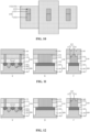
- a portion of a thickness of the third conductive pillar 133 is etched by using the third mask layer 120 (with reference to FIG. 4 ) as a mask, so as to form a third lower conductive pillar 1331 and a third upper conductive pillar 1332 stacked on one another.
- An area of a top surface of the third lower conductive layer 1331 is greater than an area of a top surface of the third upper conductive pillar 1332, and the third upper conductive pillar 1332, the third lower conductive pillar 1331 and the dielectric layer 110 form a groove 1333.
- the third conductive pillar 133 is etched, so that the dimension and the profile of the third conductive pillar 133 are changed without changing the dimensions and the profiles of the first conductive pillar 131 and the second conductive pillar 132 covered by the mask layer 120.
- a cover layer filling the groove 1333 may be formed.
- the cover layer exposes the top surface of the third upper conductive pillar 1332.
- the third upper conductive pillar 1332 will be electrically connected to a corresponding conductive structure. It should be understood that, if the third upper conductive pillar 1332 also has a relatively large dimension, the third upper conductive pillar 1332 may be electrically connected to other conductive structures, to which the third upper conductive pillar should not be electrically connected, thereby causing a short circuit. Therefore, the third upper conductive pillar 1332 and the third lower conductive pillar 1331 provided in this embodiment can reduce the resistance, while avoiding erroneous electrical connection.
- a ratio of an etching depth of the groove 1333 to the thickness of the third conductive pillar 133 is greater than 1/5, for example, the ratio may be 2/5, 1/2, 3/5. It should be understood that, the etching depth may affect the process time, may also affect the resistance and firmness of the third conductive pillar 133, and may also affect the density of the cover layer subsequently filled. When the ratio of the etching depth of the groove 1333 to the thickness of the third conductive pillar 133 falls within the above range, the process time is relatively short, so that the third conductive pillar 133 can maintain a lower resistance and greater firmness. Meanwhile, the cover layer subsequently filled in the groove 1333 may have a greater density, so that the cover layer may have a good isolation effect.
- a ratio of the area of the top surface of the third upper conductive pillar 1332 to the area of the top surface of the third lower conductive pillar 1331 is smaller than 4/5, for example, the ratio may be 1/2, 1/3 or 1/4.
- the ratio falls within the above range, the probability of erroneous electrical connection of the third upper conductive pillar 1332 can be reduced, and the resistance of the third lower conductive pillar 1331 can be further reduced.
- one third upper conductive pillar 1332 is configured to form one groove 1333.
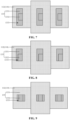
- FIG. 6 is a top view of a core area c shown in FIG. 5 .
- the left side region or right side region in FIG. 6 corresponds to the core area c shown in FIG. 5 .
- the middle region in FIG. 6 is not shown in FIG. 5 .
- the third lower conductive pillar 1331 in the middle region is electrically connected to the gate in the base 100 in the core area c. All sidewalls of one third upper conductive pillar 1332 are configured to form one groove 1333, and the groove 1333 surrounds the third upper conductive pillar 1332. That is, all the sidewalls of the third upper conductive pillar 1332, the top surface of the third lower conductive pillar 1331, and the dielectric layer 110 form one groove 1333.
- a length of the third lower conductive pillar 1331 is greater than a length of the third upper conductive pillar 1332, and a width of the third lower conductive pillar 1331 is greater than a width of the third upper conductive pillar 1332. That is, the area of the top surface of the third lower conductive pillar 1331 for forming the groove 1333 can be maximized, so that the resistance of the third lower conductive pillar 1331 can be further reduced.
- a central axis of the third upper conductive pillar 1332 in a direction perpendicular to the top surface of the base 100 coincides with a central axis of the third lower conductive pillar 1331 in the direction perpendicular to the top surface of the base 100.
- the central axis of the third upper conductive pillar may also not coincide with the center of the third lower conductive pillar.
- three sidewalls of the third upper conductive pillar 1332 are configured to form one groove 1333. That is, three sidewalls of the third upper conductive pillar 1332, the top surface of the third lower conductive pillar 1331, and the dielectric layer 110 form one groove 1333. That is, the groove 1333 surrounds only three sidewalls of the third upper conductive pillar 1332, and the other sidewall of the third upper conductive pillar 1332 is aligned with a respective sidewall of the third lower conductive pillar 1331.
- two connected sidewalls of the third upper conductive pillar 1332 are configured to form one groove 1333. That is, two connected sidewalls of the third upper conductive pillar 1332, the top surface of the third lower conductive pillar 1331, and the dielectric layer 110 form one groove 1333. In some embodiments, the other two connected sidewalls of the third upper conductive pillar 1332 are aligned with two respective sidewalls of the third lower conductive pillar 1331.
- one sidewall of the third upper conductive pillar 1332 is configured to form one groove 1333. That is, one sidewall of the third upper conductive pillar 1332, the top surface of the third lower conductive pillar 1331, and the dielectric layer 110 form one groove 1333. In some embodiments, three other sidewalls of the third upper conductive pillar 1332 are aligned with three respective sidewalls of the third lower conductive pillar 1331.
- one third upper conductive pillar 1332 is configured to form two grooves 1333, and two opposite sidewalls of the third upper conductive pillar 1333 are respectively configured to form the two grooves 1333. That is, two opposite sidewalls of the third upper conductive pillar 1332, the top surface of the third lower conductive pillar 1331, and the dielectric layer 110 form two grooves 1333.
- the central axis of the third upper conductive pillar 1332 in the direction perpendicular to the top surface of the base 100 may further coincide with the central axis of the third lower conductive pillar 1331 in the direction perpendicular to the top surface of the base 100.
- a cover layer 140 filling the groove 1333 is formed.
- the cover layer 140 exposes the top surface of the third upper conductive pillar 1332.
- an initial cover layer 141 covering the dielectric layer 110, the first conductive pillar 131, the second conductive pillar 132, the third upper conductive pillar 1332 and the third lower conductive pillar 1331 is formed.
- the initial cover layer 141 may be formed through a chemical vapor deposition process, and the initial cover layer 141 is made of an insulating material.
- the material of the initial cover layer 141 may be the same as the material of the upper dielectric layer 112. For example, both may be silicon nitride. The material of the initial cover layer 141 may also be different from the material of the upper dielectric layer 112.
- a portion of the initial cover layer 141 is removed to expose the top surface of the first conductive pillar 131, the top surface of the second conductive pillar 132, and the top surface of the third upper conductive pillar 133, and the remaining portion of the initial cover layer 141 forms the cover layer.
- planarization is performed on the initial cover layer 141, so as to remove the initial cover layer 141 higher than the top surface of the dielectric layer 110.
- planarization may be performed on the initial cover layer by chemical mechanical polishing. A portion of the initial cover layer may also be removed through an etching process.
- the third upper conductive pillar 1332 and the third lower conductive pillar 1331 are formed.
- the area of the top surface of the third upper conductive pillar 1332 is less than the area of the top surface of the third lower conductive pillar 1331, so that the probability of short circuit between the third upper conductive pillar 1332 and other conductive structures can be reduced, and the resistance of the third conductive pillar 133 can also be reduced, thereby improving the electrical performance of the third conductive pillar 133.
- the formation processes of the array area a and the peripheral area b are taken into consideration, thereby optimizing the manufacturing process of the semiconductor structure.
- FIG. 12 is a schematic diagram of a semiconductor structure according to an embodiment.
- the semiconductor structure includes: a base 100, in which a dielectric layer 110 is arranged on the base 100; a first conductive pillar 131, a second conductive pillar 132, and a third conductive pillar 133 arranged in the dielectric layer 110, in which the first conductive pillar 131 is arranged in the array area a, the second conductive pillar 132 is arranged in the peripheral area b, and the third conductive pillar 133 is arranged in the core area c, the third conductive pillar 133 includes a third lower conductive pillar 1331 and a third upper conductive pillar 1332 stacked on one another, and an area of a top surface of the third lower conductive pillar 1331 is greater than an area of a top surface of the third upper conductive pillar 1332; and
- the base of each of the array area a, the peripheral area b, and the core area c is provided with a substrate 101, an isolation structure 103, and an active area 102.
- the base 100 in the core area c is further provided with a gate, and the base 100 of the array area a is further provided with a word line 104.
- the first conductive pillar 131 is electrically connected to the active area 102.
- the second conductive pillar 132 is electrically connected to the active area 102.
- the third conductive pillar 133 is electrically connected to the gate or the active area 102.
- the third conductive pillar 133 includes a third lower conductive pillar 1331 and a third upper conductive pillar 1332 stacked on one another.
- the third upper conductive pillar 1332 and the third lower conductive pillar 1331 may be formed in the shape of a cuboid. That is, the cross-sectional shapes of the third upper conductive pillar 1332 and the third lower conductive pillar 1331 are rectangular in a direction parallel to the top surface of the base 100.
- the third upper conductive pillar 1332 and the third lower conductive pillar 1331 may also be formed in the shape of a cylinder.
- an orthographic projection of the top surface of the third upper conductive pillar 1332 on the top surface of the third lower conductive pillar 1331 falls within the top surface of the third lower conductive pillar 1331.
- the third upper conductive pillar 1332 is aligned with the third lower conductive pillar 1331, and the contact surface between the third upper conductive pillar and the third lower conductive pillar has the largest area, and the contact resistance is minimized.
- a ratio of a thickness of the third upper conductive pillar 1332 to a thickness of the third lower conductive pillar 1331 ranges from 3/5 to 2/5.
- the ratio may be 1/2.
- the third lower conductive pillar 1331 may have a relatively large volume, so that the third lower conductive pillar 1331 has relatively small resistance.
- the cover layer 140 surrounds the third upper conductive pillar 1332, and the cover layer 140 is an enclosed annular structure.
- the cover layer 140 has a relatively large volume. Since the cover layer 140 is arranged directly above the third lower conductive pillar 1331, the third lower conductive pillar 1331 may also have a relatively large volume accordingly, thereby facilitating reducing the resistance of the third lower conductive pillar 1331.
- the cover layer 140 surrounds the third upper conductive pillar 1332, the sidewalls of the third upper conductive pillar 1332 are not aligned with the sidewalls of the third lower conductive pillar 1331. In other embodiments, a part of sidewalls of the third upper conductive pillar may also be aligned with a part of sidewalls of the third lower conductive pillar.
- one sidewall of the third upper conductive pillar 1332 is aligned with one respective sidewall of the third lower conductive pillar 1331.
- two sidewalls of the third upper conductive pillar 1332 are respectively aligned with two respective sidewalls of the third lower conductive pillar 1331.
- three sidewalls of the third upper conductive pillar 1332 are respectively aligned with three respective sidewalls of the third lower conductive pillar 1331. That is, the cover layer 140 (with reference to FIG.
- the area of the top surface of the third upper conductive pillar 1332 is less than the area of the top surface of the third lower conductive pillar 1331, so that the probability of short circuit between the third upper conductive pillar 1332 and other conductive structures can be reduced, and the resistance of the third conductive pillar 133 can also be reduced, thereby improving the electrical performance of the third conductive pillar 133.
Landscapes
- Semiconductor Memories (AREA)
- Internal Circuitry In Semiconductor Integrated Circuit Devices (AREA)
Abstract
Description
- This application claims priority to Chinese Patent Application NO.
202110815094.8, filed on July 19, 2021 - Embodiments of the application relate to, but are not limited to, a method for manufacturing a semiconductor structure and a semiconductor structure.
- With the development of semiconductor technology, the process nodes of the semiconductor structure continue to shrink, and thus the integration of the semiconductor structure become higher and higher. The increase in integration mainly brings the following benefits. First, the functions of semiconductor structure can be increased. Second, according to Moore's Law, the increase in integration will directly result in cost reduction. Third, the overall power supply voltage of the semiconductor structure can be reduced, thereby reducing power consumption.
- In pursuit of smaller process nodes, the manufacturing process and the performance of the semiconductor structure need to be further improved.
- An embodiment of the application provides a method for manufacturing a semiconductor structure, the semiconductor structure including an array area, a peripheral area and a core area. The method for manufacturing the semiconductor structure includes the following operations. A base and a dielectric layer arranged on the base are provided. A first conductive pillar, a second conductive pillar and a third conductive pillar arranged in the dielectric layer are formed, in which the first conductive pillar is arranged in the array area, the second conductive pillar is arranged in the peripheral area, and the third conductive pillar is arranged in the core area. A mask layer is formed, in which the mask layer covers the dielectric layer, the first conductive pillar, the second conductive pillar and a portion of the third conductive pillar, and exposes a top surface of a portion of the third conductive pillar. A portion of a thickness of the third conductive pillar is etched by using the third mask layer as a mask to form a third lower conductive pillar and a third upper conductive pillar stacked on one another, in which an area of a top surface of the third lower conductive pillar is greater than an area of a top surface of the third upper conductive pillar, and in which the third upper conductive pillar, the third lower conductive pillar and the dielectric layer are configured to form at least one groove. A cover layer filling the at least one groove is formed, in which the cover layer exposes the top surface of the third upper conductive pillar.
- In some embodiments, the third upper conductive pillar is configured to form one groove.
- In some embodiments, all sidewalls of the third upper conductive pillar are configured to form the groove, and the groove surrounds the third upper conductive pillar.
- In some embodiments, three sidewalls of the third upper conductive pillar are configured to form the groove, or two connected sidewalls of the third upper conductive pillar are configured to form the groove, or one sidewall of the third upper conductive pillar is configured to form the groove.
- In some embodiments, the third upper conductive pillar is configured to form two grooves, and two respective opposite sidewalls of the third upper conductive pillar are respectively configured to form the two grooves.
- In some embodiments, a ratio of the area of the top surface of the third upper conductive pillar to the area of the top surface of the third lower conductive pillar is less than 4/5.
- In some embodiments, a ratio of an etching depth of the at least one groove to the thickness of the third conductive pillar is greater than 1/5.
- In some embodiments, the base is provided with a plurality of active areas, and the plurality of active areas are electrically connected to the first conductive pillar, the second conductive pillar and the third conductive pillar.
- In some embodiments, the base in the core area is provided with a gate, and the gate is electrically connected to the third conductive pillar.
- In some embodiments, the operation that the cover layer is formed includes the following operations. An initial cover layer covering the dielectric layer, the first conductive pillar, the second conductive pillar, the third upper conductive pillar and the third lower conductive pillar is formed. A portion of the initial cover layer is removed to expose a top surface of the first conductive pillar, a top surface of the second conductive pillar and the top surface of the third upper conductive pillar, in which a remaining portion of the initial cover layer forms the cover layer.
- An embodiment of the application further provides a semiconductor structure. The semiconductor structure includes: a base, in which a dielectric layer is arranged on the base; a first conductive pillar, a second conductive pillar, and a third conductive pillar arranged in the dielectric layer, in which the first conductive pillar is arranged in an array area, the second conductive pillar is arranged in a peripheral area, and the third conductive pillar is arranged in a core area, and in which the third conductive pillar includes a third lower conductive pillar and a third upper conductive pillar stacked on one another, and an area of a top surface of the third lower conductive pillar is greater than an area of a top surface of the third upper conductive pillar; and a cover layer arranged in a region formed by the third upper conductive pillar, the third lower conductive pillar, and the dielectric layer.
- In some embodiments, an orthographic projection of the top surface of the third upper conductive pillar on the top surface of the third lower conductive pillar falls within the top surface of the third lower conductive pillar.
- In some embodiments, the cover layer surrounds the third upper conductive pillar, and the cover layer is an enclosed annular structure.
- In some embodiments, each of a cross-sectional shape of the third upper conductive pillar and a cross-sectional shape of the third lower conductive pillar is formed in the shape of a rectangle in a direction parallel to a top surface of the base. A respective sidewall of the third upper conductive pillar is aligned with a respective sidewall of the third lower conductive pillar, or two respective sidewalls of the third upper conductive pillar are respectively aligned with two respective sidewalls of the third lower conductive pillar, or three respective sidewalls of the third upper conductive pillar are respectively aligned with three respective sidewalls of the third lower conductive pillar.
- In some embodiments, a ratio of a thickness of the third upper conductive pillar to a thickness of the third lower conductive pillar ranges from 3/5 to 2/5.
- One or more embodiments are exemplarity explained through the figures in accompanying drawings corresponding thereto, these exemplary explanations do not constitute a limitation to the embodiments, elements having same reference numerals in the accompanying drawings are denoted as similar elements; and unless otherwise specifically declared, the figures in the accompanying drawings do not constitute a limitation of proportion.
-
FIG. 1 to FIG. 12 are schematic diagrams corresponding to each operation in a method for manufacturing a semiconductor structure according to an embodiment of the application. - A semiconductor structure usually includes an array area, a peripheral area and a core area. The core area is closely connected to the array area. The core area is provided with unique device structures, such as a word-line driver, and the peripheral area is configured to ensure that the functions of the core area can be implemented. When the dimension of the semiconductor structure is reduced, the dimensions of these three areas have to be continuously reduced, which results in high resistance of a conductive pillar in the core area. Therefore, the electrical performance of the core area cannot be effectively improved.
- An embodiment of the application provides a method for manufacturing a semiconductor structure, which includes the following operations. A mask layer is formed, in which the mask layer covers a first conductive pillar, a second conductive pillar and a portion of a third conductive pillar. A portion of a thickness of the third conductive pillar is etched to form a third lower conductive pillar and a third upper conductive pillar. In this way, the original profiles of the first conductive pillar and the second conductive pillar can be maintained, while changing the profile and dimension of the third conductive pillar. That is, the manufacturing process of these three areas is taken into consideration. The area of the top surface of the third lower conductive pillar is greater than the area of the top surface of the third upper conductive pillar, and the third upper conductive pillar, the third lower conductive pillar and the dielectric layer are configured to form a groove. A cover layer filling the groove is formed. The relatively large dimension of the third lower conductive pillar can reduce the resistance, thereby improving the electrical performance. The cover layer exposes the third upper conductive pillar with a relatively small dimension, so that erroneous electrical connection between the third upper conductive pillar and other conductive structures can be avoided.
- Hereinafter, the respective embodiments of the application will be described in detail in connection with the accompanying drawings. However, those of ordinary skill in the art may understand that, in the respective embodiments of the application, numerous technical details are set forth in order to provide a reader with a better understanding of the application. However, the technical solutions claimed in the application can also be implemented without these technical details and various changes and modifications based on the respective embodiments below.
- The embodiments of the application provide a method for manufacturing a semiconductor structure.
FIG. 1 to FIG. 12 are schematic diagrams corresponding to each operation in the method for manufacturing the semiconductor structure according to the embodiments, which will be described in detail below with reference to the accompanying drawings. - With reference to
FIG. 1 , the semiconductor structure includes an array area a, a peripheral area b, and a core area c. In an embodiment of the application, the semiconductor structure may be a Dynamic Random Access Memory, DRAM. The array area a is configured to form a transistor, a word line, a bit line and the like. The core area c is configured to form a device structure, such as a word-line driver. The peripheral area b is configured to ensure that the functions of the core area c can be implemented. - A
base 100 and adielectric layer 110 arranged on thebase 100 are provided. In some embodiments, thebase 100 of each of the array area a, the peripheral area b, and the core area c is provided with asubstrate 101, anisolation structure 103 and anactive area 102. The material of thesubstrate 101 may be a semiconductor material, such as an elemental semiconductor material or a crystalline inorganic compound semiconductor material. The elemental semiconductor material may be silicon or germanium. The crystalline inorganic compound semiconductor material may be silicon germanium, gallium arsenide, or indium gallium, etc. Thesubstrate 101 may further contain dopant ions, such as boron or phosphorus. The material of theisolation structures 103 is an insulating material, such as silicon oxide, silicon nitride, or silicon oxynitride, etc. The material of theactive area 102 is a semiconductor material, and theactive area 102 further contains dopant ions. In some embodiments, the doping type of theactive area 102 may also be opposite to the doping type of thesubstrate 101. - Further, in an embodiment of the application, the base 100 in the core area c is further provided with a gate (not shown), and the
base 100 of the array area a is further provided with aword line 104. The material of the gate and the material of theword line 104 may be the same, which may be, for example, tungsten. In some embodiments, the material of the gate and the material of the word line may also be different from each other. - In some embodiments, a plurality of conductive pillars may be subsequently formed in the
dielectric layer 110. Thedielectric layer 110 may isolate the plurality of conductive pillars. In an embodiment of the application, thedielectric layer 110 is a bilayer structure including a lowerdielectric layer 111 and anupper dielectric layer 112 stacked on one another. In other embodiments, the dielectric layer may also be a single-layer structure, or a structure of three or more layers. The material of thedielectric layer 110 is an insulating material. For example, the material of the dielectric layer may be silicon oxide, silicon nitride, or silicon oxynitride, etc. - In an embodiment of the application, the
dielectric layer 110 of the array area a is further provided with a bitline contact layer 141 and a bit lineconductive layer 142. - With reference to
FIG. 2 and FIG. 3 , a firstconductive pillar 131, a secondconductive pillar 132, and a thirdconductive pillar 133 arranged in thedielectric layer 110 are formed. The firstconductive pillar 131 is arranged in the array area a, the secondconductive pillar 132 is arranged in the peripheral area b, and the thirdconductive pillar 133 is arranged in the core area c. - The first
conductive pillar 131 is electrically connected to theactive area 102 in the array area a, the secondconductive pillar 132 is electrically connected to theactive area 102 in the peripheral area b, and the thirdconductive pillar 133 is electrically connected to theactive area 102 and the gate in the core area c. - In some embodiments, with reference to
FIG. 2 , thedielectric layer 110 is etched by using amask 200, so as to form a first throughhole 113, a second throughhole 114, and a third throughhole 115 in thedielectric layer 110. The first throughhole 113 is arranged in the array area a, the second throughhole 114 is arranged in the peripheral area b, and the third throughhole 115 is arranged in the core area c. That is, the first throughhole 113, the second throughhole 114, and the third throughhole 115 are formed in the same operation, so that the production process can be simplified. - The first through
hole 113 is configured to be subsequently filled with the first conductive pillar, the second throughhole 114 is configured to be subsequently filled with the second conductive pillar, and the third throughhole 115 is configured to be subsequently filled with the third conductive pillar. - With reference to
FIG. 3 , the firstconductive pillar 131 filling the first through hole 113 (with reference toFIG. 2 ), the secondconductive pillar 132 filling the second through hole 114 (with reference toFIG. 2 ), and the thirdconductive pillar 133 filling the third through hole 115 (with reference toFIG. 2 ) are formed. - In an embodiment of the application, the first
conductive pillar 131, the secondconductive pillar 132, and the thirdconductive pillar 133 are formed in the same operation, so that the production process can be simplified. In some embodiments, the firstconductive pillar 131, the secondconductive pillar 132, and the thirdconductive pillar 133 may be formed through a physical vapor deposition process, or may be formed through a chemical vapor deposition process. - In an embodiment of the application, the materials of the first
conductive pillar 131, the secondconductive pillar 132, and the thirdconductive pillar 133 may be the same and are an conductive material, such as tungsten, copper, gold, silver, or polycrystalline silicon, etc. In some embodiments, the materials of the first conductive pillar, the second conductive pillar, and the third conductive pillar may also be different from each other. - In an embodiment of the application, the first
conductive pillar 131, the secondconductive pillar 132, and the thirdconductive pillar 133 may be formed in the shape of a cuboid. The first conductive pillar, the second conductive pillar, and the third conductive pillar may also be formed in the shape of a cylinder. - With reference to
FIG. 4 , amask layer 120 is formed. Themask layer 120 covers thedielectric layer 110, the firstconductive pillar 131, the secondconductive pillar 132, and a portion of the thirdconductive pillar 133. Themask layer 120 also exposes a top surface of a portion of the thirdconductive pillar 133. In this embodiment, the material of themask layer 120 is a photoresist. In other embodiments, the material of the mask layer may also be a hard mask material, such as silicon nitride, silicon oxide, or silicon oxynitride, etc. - With reference to
FIG. 5 , a portion of a thickness of the thirdconductive pillar 133 is etched by using the third mask layer 120 (with reference toFIG. 4 ) as a mask, so as to form a third lowerconductive pillar 1331 and a third upperconductive pillar 1332 stacked on one another. An area of a top surface of the third lowerconductive layer 1331 is greater than an area of a top surface of the third upperconductive pillar 1332, and the third upperconductive pillar 1332, the third lowerconductive pillar 1331 and thedielectric layer 110 form agroove 1333. - The third
conductive pillar 133 is etched, so that the dimension and the profile of the thirdconductive pillar 133 are changed without changing the dimensions and the profiles of the firstconductive pillar 131 and the secondconductive pillar 132 covered by themask layer 120. - Subsequently, a cover layer filling the
groove 1333 may be formed. The cover layer exposes the top surface of the third upperconductive pillar 1332. The third upperconductive pillar 1332 will be electrically connected to a corresponding conductive structure. It should be understood that, if the third upperconductive pillar 1332 also has a relatively large dimension, the third upperconductive pillar 1332 may be electrically connected to other conductive structures, to which the third upper conductive pillar should not be electrically connected, thereby causing a short circuit. Therefore, the third upperconductive pillar 1332 and the third lowerconductive pillar 1331 provided in this embodiment can reduce the resistance, while avoiding erroneous electrical connection. - A ratio of an etching depth of the
groove 1333 to the thickness of the thirdconductive pillar 133 is greater than 1/5, for example, the ratio may be 2/5, 1/2, 3/5. It should be understood that, the etching depth may affect the process time, may also affect the resistance and firmness of the thirdconductive pillar 133, and may also affect the density of the cover layer subsequently filled. When the ratio of the etching depth of thegroove 1333 to the thickness of the thirdconductive pillar 133 falls within the above range, the process time is relatively short, so that the thirdconductive pillar 133 can maintain a lower resistance and greater firmness. Meanwhile, the cover layer subsequently filled in thegroove 1333 may have a greater density, so that the cover layer may have a good isolation effect. - A ratio of the area of the top surface of the third upper
conductive pillar 1332 to the area of the top surface of the third lowerconductive pillar 1331 is smaller than 4/5, for example, the ratio may be 1/2, 1/3 or 1/4. When the ratio falls within the above range, the probability of erroneous electrical connection of the third upperconductive pillar 1332 can be reduced, and the resistance of the third lowerconductive pillar 1331 can be further reduced. - The relative position of the
groove 1333, the third upperconductive pillar 1332, and the third lowerconductive pillar 1331 will be described in detail below. - In an embodiment of the application, one third upper
conductive pillar 1332 is configured to form onegroove 1333. - In an example, with reference to
FIG. 5 and FIG. 6, FIG. 6 is a top view of a core area c shown inFIG. 5 . It should be noted that, the left side region or right side region inFIG. 6 corresponds to the core area c shown inFIG. 5 . The middle region inFIG. 6 is not shown inFIG. 5 . The third lowerconductive pillar 1331 in the middle region is electrically connected to the gate in the base 100 in the core area c. All sidewalls of one third upperconductive pillar 1332 are configured to form onegroove 1333, and thegroove 1333 surrounds the third upperconductive pillar 1332. That is, all the sidewalls of the third upperconductive pillar 1332, the top surface of the third lowerconductive pillar 1331, and thedielectric layer 110 form onegroove 1333. - In this case, a length of the third lower
conductive pillar 1331 is greater than a length of the third upperconductive pillar 1332, and a width of the third lowerconductive pillar 1331 is greater than a width of the third upperconductive pillar 1332. That is, the area of the top surface of the third lowerconductive pillar 1331 for forming thegroove 1333 can be maximized, so that the resistance of the third lowerconductive pillar 1331 can be further reduced. - In some embodiments, a central axis of the third upper
conductive pillar 1332 in a direction perpendicular to the top surface of thebase 100 coincides with a central axis of the third lowerconductive pillar 1331 in the direction perpendicular to the top surface of thebase 100. In other embodiments, the central axis of the third upper conductive pillar may also not coincide with the center of the third lower conductive pillar. - In some embodiments, with reference to
FIG. 7 , three sidewalls of the third upperconductive pillar 1332 are configured to form onegroove 1333. That is, three sidewalls of the third upperconductive pillar 1332, the top surface of the third lowerconductive pillar 1331, and thedielectric layer 110 form onegroove 1333. That is, thegroove 1333 surrounds only three sidewalls of the third upperconductive pillar 1332, and the other sidewall of the third upperconductive pillar 1332 is aligned with a respective sidewall of the third lowerconductive pillar 1331. - In some embodiments, with reference to
FIG. 8 , two connected sidewalls of the third upperconductive pillar 1332 are configured to form onegroove 1333. That is, two connected sidewalls of the third upperconductive pillar 1332, the top surface of the third lowerconductive pillar 1331, and thedielectric layer 110 form onegroove 1333. In some embodiments, the other two connected sidewalls of the third upperconductive pillar 1332 are aligned with two respective sidewalls of the third lowerconductive pillar 1331. - In some embodiments, with reference to
FIG. 9 , one sidewall of the third upperconductive pillar 1332 is configured to form onegroove 1333. That is, one sidewall of the third upperconductive pillar 1332, the top surface of the third lowerconductive pillar 1331, and thedielectric layer 110 form onegroove 1333. In some embodiments, three other sidewalls of the third upperconductive pillar 1332 are aligned with three respective sidewalls of the third lowerconductive pillar 1331. - In some embodiments, with reference to
FIG. 10 , one third upperconductive pillar 1332 is configured to form twogrooves 1333, and two opposite sidewalls of the third upperconductive pillar 1333 are respectively configured to form the twogrooves 1333. That is, two opposite sidewalls of the third upperconductive pillar 1332, the top surface of the third lowerconductive pillar 1331, and thedielectric layer 110 form twogrooves 1333. - In some embodiments, the central axis of the third upper
conductive pillar 1332 in the direction perpendicular to the top surface of the base 100 may further coincide with the central axis of the third lowerconductive pillar 1331 in the direction perpendicular to the top surface of thebase 100. - With reference to
FIG. 11 and FIG. 12 , acover layer 140 filling thegroove 1333 is formed. Thecover layer 140 exposes the top surface of the third upperconductive pillar 1332. - In some embodiments, with reference to
FIG. 11 , aninitial cover layer 141 covering thedielectric layer 110, the firstconductive pillar 131, the secondconductive pillar 132, the third upperconductive pillar 1332 and the third lowerconductive pillar 1331 is formed. In an embodiment of the application, theinitial cover layer 141 may be formed through a chemical vapor deposition process, and theinitial cover layer 141 is made of an insulating material. In some embodiments, the material of theinitial cover layer 141 may be the same as the material of theupper dielectric layer 112. For example, both may be silicon nitride. The material of theinitial cover layer 141 may also be different from the material of theupper dielectric layer 112. - With reference to
FIG. 12 , a portion of theinitial cover layer 141 is removed to expose the top surface of the firstconductive pillar 131, the top surface of the secondconductive pillar 132, and the top surface of the third upperconductive pillar 133, and the remaining portion of theinitial cover layer 141 forms the cover layer. In some embodiments, planarization is performed on theinitial cover layer 141, so as to remove theinitial cover layer 141 higher than the top surface of thedielectric layer 110. In some embodiments, planarization may be performed on the initial cover layer by chemical mechanical polishing. A portion of the initial cover layer may also be removed through an etching process. - In an embodiment of the application, the third upper
conductive pillar 1332 and the third lowerconductive pillar 1331 are formed. The area of the top surface of the third upperconductive pillar 1332 is less than the area of the top surface of the third lowerconductive pillar 1331, so that the probability of short circuit between the third upperconductive pillar 1332 and other conductive structures can be reduced, and the resistance of the thirdconductive pillar 133 can also be reduced, thereby improving the electrical performance of the thirdconductive pillar 133. Further, while forming the thirdconductive pillar 133, the formation processes of the array area a and the peripheral area b are taken into consideration, thereby optimizing the manufacturing process of the semiconductor structure. - An embodiment of the application provides a semiconductor structure, which may be manufactured by the method for manufacturing the semiconductor structure provided in the above embodiments.
FIG. 12 is a schematic diagram of a semiconductor structure according to an embodiment. With reference toFIG. 12 , the semiconductor structure includes: a base 100, in which adielectric layer 110 is arranged on thebase 100; a firstconductive pillar 131, a secondconductive pillar 132, and a thirdconductive pillar 133 arranged in thedielectric layer 110, in which the firstconductive pillar 131 is arranged in the array area a, the secondconductive pillar 132 is arranged in the peripheral area b, and the thirdconductive pillar 133 is arranged in the core area c, the thirdconductive pillar 133 includes a third lowerconductive pillar 1331 and a third upperconductive pillar 1332 stacked on one another, and an area of a top surface of the third lowerconductive pillar 1331 is greater than an area of a top surface of the third upperconductive pillar 1332; and acover layer 140, in which thecover layer 140 is arranged in a region formed by the third upperconductive pillar 1332, the third lowerconductive pillar 1331 and thedielectric layer 110. The parts of this embodiment that are the same as or similar to the above embodiments are described in detailed with reference to the above embodiments, which are not repeated herein. - Hereinafter, it will be described with reference to the accompanying drawings.
- In an embodiment of the application, the base of each of the array area a, the peripheral area b, and the core area c is provided with a
substrate 101, anisolation structure 103, and anactive area 102. The base 100 in the core area c is further provided with a gate, and thebase 100 of the array area a is further provided with aword line 104. - The first
conductive pillar 131 is electrically connected to theactive area 102. The secondconductive pillar 132 is electrically connected to theactive area 102. The thirdconductive pillar 133 is electrically connected to the gate or theactive area 102. - The third
conductive pillar 133 includes a third lowerconductive pillar 1331 and a third upperconductive pillar 1332 stacked on one another. In an embodiment of the application, the third upperconductive pillar 1332 and the third lowerconductive pillar 1331 may be formed in the shape of a cuboid. That is, the cross-sectional shapes of the third upperconductive pillar 1332 and the third lowerconductive pillar 1331 are rectangular in a direction parallel to the top surface of thebase 100. The third upperconductive pillar 1332 and the third lowerconductive pillar 1331 may also be formed in the shape of a cylinder. - In an embodiment of the application, an orthographic projection of the top surface of the third upper
conductive pillar 1332 on the top surface of the third lowerconductive pillar 1331 falls within the top surface of the third lowerconductive pillar 1331. In this case, the third upperconductive pillar 1332 is aligned with the third lowerconductive pillar 1331, and the contact surface between the third upper conductive pillar and the third lower conductive pillar has the largest area, and the contact resistance is minimized. - A ratio of a thickness of the third upper
conductive pillar 1332 to a thickness of the third lowerconductive pillar 1331 ranges from 3/5 to 2/5. For example, the ratio may be 1/2. When the thickness ratio falls within the above range, the third lowerconductive pillar 1331 may have a relatively large volume, so that the third lowerconductive pillar 1331 has relatively small resistance. - In an embodiment of the application, the
cover layer 140 surrounds the third upperconductive pillar 1332, and thecover layer 140 is an enclosed annular structure. When thecover layer 140 is an enclosed annular structure, thecover layer 140 has a relatively large volume. Since thecover layer 140 is arranged directly above the third lowerconductive pillar 1331, the third lowerconductive pillar 1331 may also have a relatively large volume accordingly, thereby facilitating reducing the resistance of the third lowerconductive pillar 1331. When thecover layer 140 surrounds the third upperconductive pillar 1332, the sidewalls of the third upperconductive pillar 1332 are not aligned with the sidewalls of the third lowerconductive pillar 1331. In other embodiments, a part of sidewalls of the third upper conductive pillar may also be aligned with a part of sidewalls of the third lower conductive pillar. - In some embodiments, with reference to
FIG. 7 , one sidewall of the third upperconductive pillar 1332 is aligned with one respective sidewall of the third lowerconductive pillar 1331. With reference toFIG. 8 and FIG. 9 , two sidewalls of the third upperconductive pillar 1332 are respectively aligned with two respective sidewalls of the third lowerconductive pillar 1331. With reference toFIG. 10 , three sidewalls of the third upperconductive pillar 1332 are respectively aligned with three respective sidewalls of the third lowerconductive pillar 1331. That is, the cover layer 140 (with reference toFIG. 12 ) surrounds only a part of sidewalls of the third upperconductive pillar 1332, and the remaining part of sidewalls of the third upperconductive pillar 1332 which are not surrounded by thecover layer 140 is aligned with a part of sidewalls of the third lowerconductive pillar 1331. - In some embodiments, the area of the top surface of the third upper
conductive pillar 1332 is less than the area of the top surface of the third lowerconductive pillar 1331, so that the probability of short circuit between the third upperconductive pillar 1332 and other conductive structures can be reduced, and the resistance of the thirdconductive pillar 133 can also be reduced, thereby improving the electrical performance of the thirdconductive pillar 133. - Those of ordinary skill in the art may understand that the above embodiments are some embodiments of the application. In practical applications, various changes may be made in forms and detail without departing from the spirit and scope of the application. Any person skilled in the art may make changes and modifications without departing from the spirit and scope of the application. Therefore, the protection scope of application should be subjected to the scope defined by the appended claims.
Claims (15)
- A method for manufacturing a semiconductor structure, the semiconductor structure comprising an array area, a peripheral area and a core area, the method for manufacturing the semiconductor structure comprising:providing a base and a dielectric layer arranged on the base;forming a first conductive pillar, a second conductive pillar and a third conductive pillar arranged in the dielectric layer, wherein the first conductive pillar is arranged in the array area, the second conductive pillar is arranged in the peripheral area, and the third conductive pillar is arranged in the core area;forming a mask layer, wherein the mask layer covers the dielectric layer, the first conductive pillar, the second conductive pillar and a portion of the third conductive pillar, and exposes a top surface of a portion of the third conductive pillar;etching a portion of a thickness of the third conductive pillar by using the third mask layer as a mask to form a third lower conductive pillar and a third upper conductive pillar stacked on one another, wherein an area of a top surface of the third lower conductive pillar is greater than an area of a top surface of the third upper conductive pillar, and wherein the third upper conductive pillar, the third lower conductive pillar and the dielectric layer are configured to form at least one groove; andforming a cover layer filling the at least one groove, wherein the cover layer exposes the top surface of the third upper conductive pillar.
- The method for manufacturing the semiconductor structure of claim 1, wherein the third upper conductive pillar is configured to form one groove.
- The method for manufacturing the semiconductor structure of claim 2, wherein all sidewalls of the third upper conductive pillar are configured to form the groove, and the groove surrounds the third upper conductive pillar.
- The method for manufacturing the semiconductor structure of claim 2, wherein three sidewalls of the third upper conductive pillar are configured to form the groove, or two connected sidewalls of the third upper conductive pillar are configured to form the groove, or one sidewall of the third upper conductive pillar is configured to form the groove.
- The method for manufacturing the semiconductor structure of claim 1, wherein the third upper conductive pillar is configured to form two grooves, and two respective opposite sidewalls of the third upper conductive pillar are respectively configured to form the two grooves.
- The method for manufacturing the semiconductor structure of claim 1, wherein a ratio of the area of the top surface of the third upper conductive pillar to the area of the top surface of the third lower conductive pillar is less than 4/5.
- The method for manufacturing the semiconductor structure of claim 1, wherein a ratio of an etching depth of the at least one groove to the thickness of the third conductive pillar is greater than 1/5.
- The method for manufacturing the semiconductor structure of claim 1, wherein the base is provided with a plurality of active areas, and the plurality of active areas are electrically connected to the first conductive pillar, the second conductive pillar and the third conductive pillar.
- The method for manufacturing the semiconductor structure of claim 1, wherein the base in the core area is provided with a gate, and the gate is electrically connected to the third conductive pillar.
- The method for manufacturing the semiconductor structure of claim 1, wherein forming the cover layer comprises: forming an initial cover layer covering the dielectric layer, the first conductive pillar, the second conductive pillar, the third upper conductive pillar, and the third lower conductive pillar, and removing a portion of the initial cover layer to expose a top surface of the first conductive pillar, a top surface of the second conductive pillar and the top surface of the third upper conductive pillar, wherein a remaining portion of the initial cover layer forms the cover layer.
- A semiconductor structure, comprising an array area, a peripheral area, and a core area, and further comprising:a base, wherein a dielectric layer is arranged on the base;a first conductive pillar, a second conductive pillar, and a third conductive pillar arranged in the dielectric layer, wherein the first conductive pillar is arranged in the array area, the second conductive pillar is arranged in the peripheral area, and the third conductive pillar is arranged in the core area; andwherein the third conductive pillar comprises a third lower conductive pillar and a third upper conductive pillar stacked on one another, and an area of a top surface of the third lower conductive pillar is greater than an area of a top surface of the third upper conductive pillar; anda cover layer arranged in a region formed by the third upper conductive pillar, the third lower conductive pillar, and the dielectric layer.
- The semiconductor structure of claim 11, wherein an orthographic projection of the top surface of the third upper conductive pillar on the top surface of the third lower conductive pillar falls within the top surface of the third lower conductive pillar.
- The semiconductor structure of claim 12, wherein the cover layer surrounds the third upper conductive pillar, and the cover layer is an enclosed annular structure.
- The semiconductor structure of claim 11, wherein each of a cross-sectional shape of the third upper conductive pillar and a cross-sectional shape of the third lower conductive pillar is formed in the shape of a rectangle in a direction parallel to a top surface of the base, and wherein a respective sidewall of the third upper conductive pillar is aligned with a respective sidewall of the third lower conductive pillar, or two respective sidewalls of the third upper conductive pillar are respectively aligned with two respective sidewalls of the third lower conductive pillar, or three respective sidewalls of the third upper conductive pillar are respectively aligned with three respective sidewalls of the third lower conductive pillar.
- The semiconductor structure of claim 11, wherein a ratio of a thickness of the third upper conductive pillar to a thickness of the third lower conductive pillar ranges from 3/5 to 2/5.
Applications Claiming Priority (2)
| Application Number | Priority Date | Filing Date | Title |
|---|---|---|---|
| CN202110815094.8A CN115643750B (en) | 2021-07-19 | 2021-07-19 | Semiconductor structure manufacturing methods and semiconductor structures |
| PCT/CN2021/124053 WO2023000515A1 (en) | 2021-07-19 | 2021-10-15 | Method for fabricating semiconductor structure and semiconductor structure |
Publications (2)
| Publication Number | Publication Date |
|---|---|
| EP4258839A1 true EP4258839A1 (en) | 2023-10-11 |
| EP4258839A4 EP4258839A4 (en) | 2024-07-24 |
Family
ID=84939690
Family Applications (1)
| Application Number | Title | Priority Date | Filing Date |
|---|---|---|---|
| EP21950753.0A Pending EP4258839A4 (en) | 2021-07-19 | 2021-10-15 | METHOD FOR PRODUCING A SEMICONDUCTOR STRUCTURE AND SEMICONDUCTOR STRUCTURE |
Country Status (4)
| Country | Link |
|---|---|
| US (1) | US12538769B2 (en) |
| EP (1) | EP4258839A4 (en) |
| CN (1) | CN115643750B (en) |
| WO (1) | WO2023000515A1 (en) |
Family Cites Families (24)
| Publication number | Priority date | Publication date | Assignee | Title |
|---|---|---|---|---|
| JP2006229260A (en) * | 1997-10-31 | 2006-08-31 | Samsung Electronics Co Ltd | Method for manufacturing DRAM device |
| KR100382724B1 (en) | 2000-11-21 | 2003-05-09 | 삼성전자주식회사 | Method of manufacturing semiconductor device including various contact studs |
| KR100527668B1 (en) * | 2003-03-07 | 2005-11-28 | 삼성전자주식회사 | Semiconductor device having capacitor-under-bitline structure and method of manufacturing the same |
| KR100520227B1 (en) * | 2003-12-26 | 2005-10-11 | 삼성전자주식회사 | Method for fabricating semiconductor memory device and structure therefore |
| JP2008085175A (en) * | 2006-09-28 | 2008-04-10 | Tokyo Electron Ltd | Semiconductor device manufacturing method, semiconductor device, substrate processing system, program, and storage medium. |
| JP2009147269A (en) | 2007-12-18 | 2009-07-02 | Elpida Memory Inc | Semiconductor device and manufacturing method thereof |
| KR100948078B1 (en) * | 2008-05-21 | 2010-03-16 | 주식회사 하이닉스반도체 | Manufacturing Method of Semiconductor Device |
| KR101525499B1 (en) | 2009-02-27 | 2015-06-03 | 삼성전자주식회사 | Method for manufacturing semiconductor device having capacitor under bit line structure |
| US10163688B2 (en) * | 2013-03-15 | 2018-12-25 | Taiwan Semiconductor Manufacturing Company Limited | Interconnect structure with kinked profile |
| US9515085B2 (en) | 2014-09-26 | 2016-12-06 | Sandisk Technologies Llc | Vertical memory device with bit line air gap |
| US9484296B2 (en) * | 2015-02-12 | 2016-11-01 | Sandisk Technologies Llc | Self-aligned integrated line and via structure for a three-dimensional semiconductor device |
| US9786680B2 (en) * | 2015-09-10 | 2017-10-10 | Toshiba Memory Corporation | Semiconductor device |
| CN107946237A (en) * | 2017-11-23 | 2018-04-20 | 长江存储科技有限责任公司 | Three-dimensional storage organization bus connection method, storage organization, memory and electronic equipment |
| US10535669B2 (en) | 2017-11-23 | 2020-01-14 | Yangtze Memory Technologies Co., Ltd. | Three-dimensional memory devices and fabricating methods thereof |
| US10741417B2 (en) | 2017-11-30 | 2020-08-11 | Taiwan Semiconductor Manufacturing Co., Ltd. | Method for forming interconnect structure |
| US10354956B1 (en) | 2018-01-05 | 2019-07-16 | Sandisk Technologies Llc | Three-dimensional memory device containing hydrogen diffusion barrier structures for CMOS under array architecture and method of making the same |
| US10535660B1 (en) | 2018-08-30 | 2020-01-14 | Nanya Technology Corporation | Dynamic random access memory structure and method for preparing the same |
| KR102661847B1 (en) | 2018-09-11 | 2024-04-30 | 삼성전자주식회사 | Semiconductor device |
| KR102334784B1 (en) | 2018-12-31 | 2021-12-07 | 마이크론 테크놀로지, 인크. | 3D Dynamic Random Access Memory Array |
| CN120614821A (en) * | 2019-09-27 | 2025-09-09 | 福建省晋华集成电路有限公司 | semiconductor devices |
| US11328749B2 (en) * | 2019-12-18 | 2022-05-10 | Micron Technology, Inc. | Conductive interconnects and methods of forming conductive interconnects |
| US11476365B2 (en) * | 2020-01-16 | 2022-10-18 | Taiwan Semiconductor Manufacturing Co., Ltd. | Fin field effect transistor device structure and method for forming the same |
| TWI752464B (en) * | 2020-04-14 | 2022-01-11 | 華邦電子股份有限公司 | Semiconductor structures and methods for forming the same |
| EP4050653B1 (en) * | 2020-12-30 | 2024-01-31 | Changxin Memory Technologies, Inc. | Method for preparing semiconductor structure, and semiconductor structure |
-
2021
- 2021-07-19 CN CN202110815094.8A patent/CN115643750B/en active Active
- 2021-10-15 EP EP21950753.0A patent/EP4258839A4/en active Pending
- 2021-10-15 WO PCT/CN2021/124053 patent/WO2023000515A1/en not_active Ceased
-
2022
- 2022-06-20 US US17/807,794 patent/US12538769B2/en active Active
Also Published As
| Publication number | Publication date |
|---|---|
| EP4258839A4 (en) | 2024-07-24 |
| WO2023000515A1 (en) | 2023-01-26 |
| US12538769B2 (en) | 2026-01-27 |
| CN115643750B (en) | 2025-11-14 |
| US20230018338A1 (en) | 2023-01-19 |
| CN115643750A (en) | 2023-01-24 |
Similar Documents
| Publication | Publication Date | Title |
|---|---|---|
| US8552472B2 (en) | Integrated circuit devices including vertical channel transistors with shield lines interposed between bit lines and methods of fabricating the same | |
| US9634012B2 (en) | Method of forming active patterns, active pattern array, and method of manufacturing a semiconductor device | |
| JP5520185B2 (en) | Semiconductor device and manufacturing method thereof | |
| US12137550B2 (en) | Semiconductor structure with a first lower electrode layer and a second lower electrode layer and method for manufacturing same | |
| US9461051B2 (en) | Methods of forming electronic devices having pads using first and second masks | |
| US7582925B2 (en) | Integrated circuit devices including insulating support layers | |
| US9048293B2 (en) | Semiconductor device and method for manufacturing the same | |
| US10312105B2 (en) | Semiconductor devices using auxiliary layers for trimming margin and devices so formed | |
| CN116322041B (en) | Memory, manufacturing method thereof and electronic equipment | |
| KR20230165456A (en) | Semiconductor devices and methods of manufacturing the same | |
| CN115172370A (en) | Semiconductor structure and forming method thereof | |
| CN116782644A (en) | Semiconductor devices and manufacturing methods thereof, electronic equipment | |
| US12101924B2 (en) | Semiconductor structure and method for manufacturing same | |
| US12538769B2 (en) | Method for manufacturing conductive pillar structure for semiconductor substrate and conductive pillar structure for semiconductor substrate | |
| CN115581073B (en) | Storage Element and Manufacturing Method Thereof | |
| CN212570997U (en) | Semiconductor memory device with a plurality of memory cells | |
| CN115643749B (en) | Semiconductor structure manufacturing methods and semiconductor structures | |
| US12238915B2 (en) | Method for manufacturing semiconductor structure and same | |
| KR20230031602A (en) | Ferroelectric memory device and method of fabricating the same | |
| US12347766B2 (en) | Semiconductor structure and method for forming the same | |
| US12543302B2 (en) | Memory device having planarized fins and method of manufacturing the same | |
| KR100570219B1 (en) | Chain gate line of semiconductor device and manufacturing method thereof | |
| US20250240945A1 (en) | Semiconductor device | |
| JP2025072325A (en) | Semiconductor Device | |
| CN117690908A (en) | Semiconductor structures and manufacturing methods |
Legal Events
| Date | Code | Title | Description |
|---|---|---|---|
| STAA | Information on the status of an ep patent application or granted ep patent |
Free format text: STATUS: THE INTERNATIONAL PUBLICATION HAS BEEN MADE |
|
| PUAI | Public reference made under article 153(3) epc to a published international application that has entered the european phase |
Free format text: ORIGINAL CODE: 0009012 |
|
| STAA | Information on the status of an ep patent application or granted ep patent |
Free format text: STATUS: REQUEST FOR EXAMINATION WAS MADE |
|
| 17P | Request for examination filed |
Effective date: 20230705 |
|
| AK | Designated contracting states |
Kind code of ref document: A1 Designated state(s): AL AT BE BG CH CY CZ DE DK EE ES FI FR GB GR HR HU IE IS IT LI LT LU LV MC MK MT NL NO PL PT RO RS SE SI SK SM TR |
|
| A4 | Supplementary search report drawn up and despatched |
Effective date: 20240625 |
|
| RIC1 | Information provided on ipc code assigned before grant |
Ipc: H01L 21/768 20060101ALN20240619BHEP Ipc: H01L 23/485 20060101ALI20240619BHEP Ipc: H01L 23/528 20060101ALI20240619BHEP Ipc: H10B 12/00 20230101AFI20240619BHEP |
|
| DAV | Request for validation of the european patent (deleted) | ||
| DAX | Request for extension of the european patent (deleted) | ||
| STAA | Information on the status of an ep patent application or granted ep patent |
Free format text: STATUS: EXAMINATION IS IN PROGRESS |
|
| 17Q | First examination report despatched |
Effective date: 20250307 |