EP4258336A2 - Radio frequency module - Google Patents
Radio frequency module Download PDFInfo
- Publication number
- EP4258336A2 EP4258336A2 EP23192886.2A EP23192886A EP4258336A2 EP 4258336 A2 EP4258336 A2 EP 4258336A2 EP 23192886 A EP23192886 A EP 23192886A EP 4258336 A2 EP4258336 A2 EP 4258336A2
- Authority
- EP
- European Patent Office
- Prior art keywords
- die
- substrate
- package substrate
- module
- packaged
- Prior art date
- Legal status (The legal status is an assumption and is not a legal conclusion. Google has not performed a legal analysis and makes no representation as to the accuracy of the status listed.)
- Pending
Links
Images




Classifications
-
- H—ELECTRICITY
- H10—SEMICONDUCTOR DEVICES; ELECTRIC SOLID-STATE DEVICES NOT OTHERWISE PROVIDED FOR
- H10W—GENERIC PACKAGES, INTERCONNECTIONS, CONNECTORS OR OTHER CONSTRUCTIONAL DETAILS OF DEVICES COVERED BY CLASS H10
- H10W44/00—Electrical arrangements for controlling or matching impedance
- H10W44/20—Electrical arrangements for controlling or matching impedance at high-frequency [HF] or radio frequency [RF]
-
- H—ELECTRICITY
- H03—ELECTRONIC CIRCUITRY
- H03F—AMPLIFIERS
- H03F3/00—Amplifiers with only discharge tubes or only semiconductor devices as amplifying elements
- H03F3/189—High-frequency amplifiers, e.g. radio frequency amplifiers
- H03F3/19—High-frequency amplifiers, e.g. radio frequency amplifiers with semiconductor devices only
- H03F3/195—High-frequency amplifiers, e.g. radio frequency amplifiers with semiconductor devices only in integrated circuits
-
- H—ELECTRICITY
- H03—ELECTRONIC CIRCUITRY
- H03F—AMPLIFIERS
- H03F3/00—Amplifiers with only discharge tubes or only semiconductor devices as amplifying elements
- H03F3/20—Power amplifiers, e.g. Class B amplifiers, Class C amplifiers
- H03F3/24—Power amplifiers, e.g. Class B amplifiers, Class C amplifiers of transmitter output stages
- H03F3/245—Power amplifiers, e.g. Class B amplifiers, Class C amplifiers of transmitter output stages with semiconductor devices only
-
- H—ELECTRICITY
- H10—SEMICONDUCTOR DEVICES; ELECTRIC SOLID-STATE DEVICES NOT OTHERWISE PROVIDED FOR
- H10W—GENERIC PACKAGES, INTERCONNECTIONS, CONNECTORS OR OTHER CONSTRUCTIONAL DETAILS OF DEVICES COVERED BY CLASS H10
- H10W20/00—Interconnections in chips, wafers or substrates
- H10W20/20—Interconnections within wafers or substrates, e.g. through-silicon vias [TSV]
-
- H—ELECTRICITY
- H10—SEMICONDUCTOR DEVICES; ELECTRIC SOLID-STATE DEVICES NOT OTHERWISE PROVIDED FOR
- H10W—GENERIC PACKAGES, INTERCONNECTIONS, CONNECTORS OR OTHER CONSTRUCTIONAL DETAILS OF DEVICES COVERED BY CLASS H10
- H10W40/00—Arrangements for thermal protection or thermal control
- H10W40/20—Arrangements for cooling
- H10W40/22—Arrangements for cooling characterised by their shape, e.g. having conical or cylindrical projections
-
- H—ELECTRICITY
- H10—SEMICONDUCTOR DEVICES; ELECTRIC SOLID-STATE DEVICES NOT OTHERWISE PROVIDED FOR
- H10W—GENERIC PACKAGES, INTERCONNECTIONS, CONNECTORS OR OTHER CONSTRUCTIONAL DETAILS OF DEVICES COVERED BY CLASS H10
- H10W40/00—Arrangements for thermal protection or thermal control
- H10W40/20—Arrangements for cooling
- H10W40/22—Arrangements for cooling characterised by their shape, e.g. having conical or cylindrical projections
- H10W40/226—Arrangements for cooling characterised by their shape, e.g. having conical or cylindrical projections characterised by projecting parts, e.g. fins to increase surface area
- H10W40/228—Arrangements for cooling characterised by their shape, e.g. having conical or cylindrical projections characterised by projecting parts, e.g. fins to increase surface area the projecting parts being wire-shaped or pin-shaped
-
- H—ELECTRICITY
- H10—SEMICONDUCTOR DEVICES; ELECTRIC SOLID-STATE DEVICES NOT OTHERWISE PROVIDED FOR
- H10W—GENERIC PACKAGES, INTERCONNECTIONS, CONNECTORS OR OTHER CONSTRUCTIONAL DETAILS OF DEVICES COVERED BY CLASS H10
- H10W70/00—Package substrates; Interposers; Redistribution layers [RDL]
- H10W70/60—Insulating or insulated package substrates; Interposers; Redistribution layers
- H10W70/67—Insulating or insulated package substrates; Interposers; Redistribution layers characterised by their insulating layers or insulating parts
- H10W70/68—Shapes or dispositions thereof
-
- H—ELECTRICITY
- H10—SEMICONDUCTOR DEVICES; ELECTRIC SOLID-STATE DEVICES NOT OTHERWISE PROVIDED FOR
- H10W—GENERIC PACKAGES, INTERCONNECTIONS, CONNECTORS OR OTHER CONSTRUCTIONAL DETAILS OF DEVICES COVERED BY CLASS H10
- H10W76/00—Containers; Fillings or auxiliary members therefor; Seals
- H10W76/10—Containers or parts thereof
- H10W76/12—Containers or parts thereof characterised by their shape
- H10W76/15—Containers comprising an insulating or insulated base
-
- H—ELECTRICITY
- H10—SEMICONDUCTOR DEVICES; ELECTRIC SOLID-STATE DEVICES NOT OTHERWISE PROVIDED FOR
- H10W—GENERIC PACKAGES, INTERCONNECTIONS, CONNECTORS OR OTHER CONSTRUCTIONAL DETAILS OF DEVICES COVERED BY CLASS H10
- H10W76/00—Containers; Fillings or auxiliary members therefor; Seals
- H10W76/40—Fillings or auxiliary members in containers, e.g. centering rings
- H10W76/42—Fillings
- H10W76/47—Solid or gel fillings
-
- H—ELECTRICITY
- H03—ELECTRONIC CIRCUITRY
- H03F—AMPLIFIERS
- H03F2200/00—Indexing scheme relating to amplifiers
- H03F2200/451—Indexing scheme relating to amplifiers the amplifier being a radio frequency amplifier
-
- H—ELECTRICITY
- H10—SEMICONDUCTOR DEVICES; ELECTRIC SOLID-STATE DEVICES NOT OTHERWISE PROVIDED FOR
- H10W—GENERIC PACKAGES, INTERCONNECTIONS, CONNECTORS OR OTHER CONSTRUCTIONAL DETAILS OF DEVICES COVERED BY CLASS H10
- H10W44/00—Electrical arrangements for controlling or matching impedance
- H10W44/20—Electrical arrangements for controlling or matching impedance at high-frequency [HF] or radio frequency [RF]
- H10W44/203—Electrical connections
- H10W44/206—Wires
-
- H—ELECTRICITY
- H10—SEMICONDUCTOR DEVICES; ELECTRIC SOLID-STATE DEVICES NOT OTHERWISE PROVIDED FOR
- H10W—GENERIC PACKAGES, INTERCONNECTIONS, CONNECTORS OR OTHER CONSTRUCTIONAL DETAILS OF DEVICES COVERED BY CLASS H10
- H10W44/00—Electrical arrangements for controlling or matching impedance
- H10W44/20—Electrical arrangements for controlling or matching impedance at high-frequency [HF] or radio frequency [RF]
- H10W44/203—Electrical connections
- H10W44/209—Vertical interconnections, e.g. vias
-
- H—ELECTRICITY
- H10—SEMICONDUCTOR DEVICES; ELECTRIC SOLID-STATE DEVICES NOT OTHERWISE PROVIDED FOR
- H10W—GENERIC PACKAGES, INTERCONNECTIONS, CONNECTORS OR OTHER CONSTRUCTIONAL DETAILS OF DEVICES COVERED BY CLASS H10
- H10W44/00—Electrical arrangements for controlling or matching impedance
- H10W44/20—Electrical arrangements for controlling or matching impedance at high-frequency [HF] or radio frequency [RF]
- H10W44/203—Electrical connections
- H10W44/216—Waveguides, e.g. strip lines
-
- H—ELECTRICITY
- H10—SEMICONDUCTOR DEVICES; ELECTRIC SOLID-STATE DEVICES NOT OTHERWISE PROVIDED FOR
- H10W—GENERIC PACKAGES, INTERCONNECTIONS, CONNECTORS OR OTHER CONSTRUCTIONAL DETAILS OF DEVICES COVERED BY CLASS H10
- H10W44/00—Electrical arrangements for controlling or matching impedance
- H10W44/20—Electrical arrangements for controlling or matching impedance at high-frequency [HF] or radio frequency [RF]
- H10W44/226—Electrical arrangements for controlling or matching impedance at high-frequency [HF] or radio frequency [RF] for HF amplifiers
-
- H—ELECTRICITY
- H10—SEMICONDUCTOR DEVICES; ELECTRIC SOLID-STATE DEVICES NOT OTHERWISE PROVIDED FOR
- H10W—GENERIC PACKAGES, INTERCONNECTIONS, CONNECTORS OR OTHER CONSTRUCTIONAL DETAILS OF DEVICES COVERED BY CLASS H10
- H10W44/00—Electrical arrangements for controlling or matching impedance
- H10W44/20—Electrical arrangements for controlling or matching impedance at high-frequency [HF] or radio frequency [RF]
- H10W44/251—Electrical arrangements for controlling or matching impedance at high-frequency [HF] or radio frequency [RF] for monolithic microwave integrated circuits [MMIC]
-
- H—ELECTRICITY
- H10—SEMICONDUCTOR DEVICES; ELECTRIC SOLID-STATE DEVICES NOT OTHERWISE PROVIDED FOR
- H10W—GENERIC PACKAGES, INTERCONNECTIONS, CONNECTORS OR OTHER CONSTRUCTIONAL DETAILS OF DEVICES COVERED BY CLASS H10
- H10W72/00—Interconnections or connectors in packages
- H10W72/01—Manufacture or treatment
- H10W72/015—Manufacture or treatment of bond wires
- H10W72/01515—Forming coatings
-
- H—ELECTRICITY
- H10—SEMICONDUCTOR DEVICES; ELECTRIC SOLID-STATE DEVICES NOT OTHERWISE PROVIDED FOR
- H10W—GENERIC PACKAGES, INTERCONNECTIONS, CONNECTORS OR OTHER CONSTRUCTIONAL DETAILS OF DEVICES COVERED BY CLASS H10
- H10W72/00—Interconnections or connectors in packages
- H10W72/071—Connecting or disconnecting
- H10W72/072—Connecting or disconnecting of bump connectors
-
- H—ELECTRICITY
- H10—SEMICONDUCTOR DEVICES; ELECTRIC SOLID-STATE DEVICES NOT OTHERWISE PROVIDED FOR
- H10W—GENERIC PACKAGES, INTERCONNECTIONS, CONNECTORS OR OTHER CONSTRUCTIONAL DETAILS OF DEVICES COVERED BY CLASS H10
- H10W72/00—Interconnections or connectors in packages
- H10W72/071—Connecting or disconnecting
- H10W72/072—Connecting or disconnecting of bump connectors
- H10W72/07251—Connecting or disconnecting of bump connectors characterised by changes in properties of the bump connectors during connecting
- H10W72/07254—Connecting or disconnecting of bump connectors characterised by changes in properties of the bump connectors during connecting changes in dispositions
-
- H—ELECTRICITY
- H10—SEMICONDUCTOR DEVICES; ELECTRIC SOLID-STATE DEVICES NOT OTHERWISE PROVIDED FOR
- H10W—GENERIC PACKAGES, INTERCONNECTIONS, CONNECTORS OR OTHER CONSTRUCTIONAL DETAILS OF DEVICES COVERED BY CLASS H10
- H10W72/00—Interconnections or connectors in packages
- H10W72/071—Connecting or disconnecting
- H10W72/073—Connecting or disconnecting of die-attach connectors
-
- H—ELECTRICITY
- H10—SEMICONDUCTOR DEVICES; ELECTRIC SOLID-STATE DEVICES NOT OTHERWISE PROVIDED FOR
- H10W—GENERIC PACKAGES, INTERCONNECTIONS, CONNECTORS OR OTHER CONSTRUCTIONAL DETAILS OF DEVICES COVERED BY CLASS H10
- H10W72/00—Interconnections or connectors in packages
- H10W72/071—Connecting or disconnecting
- H10W72/075—Connecting or disconnecting of bond wires
-
- H—ELECTRICITY
- H10—SEMICONDUCTOR DEVICES; ELECTRIC SOLID-STATE DEVICES NOT OTHERWISE PROVIDED FOR
- H10W—GENERIC PACKAGES, INTERCONNECTIONS, CONNECTORS OR OTHER CONSTRUCTIONAL DETAILS OF DEVICES COVERED BY CLASS H10
- H10W72/00—Interconnections or connectors in packages
- H10W72/20—Bump connectors, e.g. solder bumps or copper pillars; Dummy bumps; Thermal bumps
- H10W72/221—Structures or relative sizes
-
- H—ELECTRICITY
- H10—SEMICONDUCTOR DEVICES; ELECTRIC SOLID-STATE DEVICES NOT OTHERWISE PROVIDED FOR
- H10W—GENERIC PACKAGES, INTERCONNECTIONS, CONNECTORS OR OTHER CONSTRUCTIONAL DETAILS OF DEVICES COVERED BY CLASS H10
- H10W72/00—Interconnections or connectors in packages
- H10W72/20—Bump connectors, e.g. solder bumps or copper pillars; Dummy bumps; Thermal bumps
- H10W72/241—Dispositions, e.g. layouts
- H10W72/247—Dispositions of multiple bumps
-
- H—ELECTRICITY
- H10—SEMICONDUCTOR DEVICES; ELECTRIC SOLID-STATE DEVICES NOT OTHERWISE PROVIDED FOR
- H10W—GENERIC PACKAGES, INTERCONNECTIONS, CONNECTORS OR OTHER CONSTRUCTIONAL DETAILS OF DEVICES COVERED BY CLASS H10
- H10W72/00—Interconnections or connectors in packages
- H10W72/30—Die-attach connectors
- H10W72/331—Shapes of die-attach connectors
-
- H—ELECTRICITY
- H10—SEMICONDUCTOR DEVICES; ELECTRIC SOLID-STATE DEVICES NOT OTHERWISE PROVIDED FOR
- H10W—GENERIC PACKAGES, INTERCONNECTIONS, CONNECTORS OR OTHER CONSTRUCTIONAL DETAILS OF DEVICES COVERED BY CLASS H10
- H10W72/00—Interconnections or connectors in packages
- H10W72/30—Die-attach connectors
- H10W72/331—Shapes of die-attach connectors
- H10W72/332—Plan-view shape, i.e. in top view
-
- H—ELECTRICITY
- H10—SEMICONDUCTOR DEVICES; ELECTRIC SOLID-STATE DEVICES NOT OTHERWISE PROVIDED FOR
- H10W—GENERIC PACKAGES, INTERCONNECTIONS, CONNECTORS OR OTHER CONSTRUCTIONAL DETAILS OF DEVICES COVERED BY CLASS H10
- H10W72/00—Interconnections or connectors in packages
- H10W72/30—Die-attach connectors
- H10W72/351—Materials of die-attach connectors
- H10W72/353—Materials of die-attach connectors not comprising solid metals or solid metalloids, e.g. ceramics
- H10W72/354—Materials of die-attach connectors not comprising solid metals or solid metalloids, e.g. ceramics comprising polymers
-
- H—ELECTRICITY
- H10—SEMICONDUCTOR DEVICES; ELECTRIC SOLID-STATE DEVICES NOT OTHERWISE PROVIDED FOR
- H10W—GENERIC PACKAGES, INTERCONNECTIONS, CONNECTORS OR OTHER CONSTRUCTIONAL DETAILS OF DEVICES COVERED BY CLASS H10
- H10W72/00—Interconnections or connectors in packages
- H10W72/30—Die-attach connectors
- H10W72/381—Auxiliary members
- H10W72/387—Flow barriers
-
- H—ELECTRICITY
- H10—SEMICONDUCTOR DEVICES; ELECTRIC SOLID-STATE DEVICES NOT OTHERWISE PROVIDED FOR
- H10W—GENERIC PACKAGES, INTERCONNECTIONS, CONNECTORS OR OTHER CONSTRUCTIONAL DETAILS OF DEVICES COVERED BY CLASS H10
- H10W72/00—Interconnections or connectors in packages
- H10W72/50—Bond wires
- H10W72/59—Bond pads specially adapted therefor
-
- H—ELECTRICITY
- H10—SEMICONDUCTOR DEVICES; ELECTRIC SOLID-STATE DEVICES NOT OTHERWISE PROVIDED FOR
- H10W—GENERIC PACKAGES, INTERCONNECTIONS, CONNECTORS OR OTHER CONSTRUCTIONAL DETAILS OF DEVICES COVERED BY CLASS H10
- H10W72/00—Interconnections or connectors in packages
- H10W72/851—Dispositions of multiple connectors or interconnections
- H10W72/874—On different surfaces
- H10W72/884—Die-attach connectors and bond wires
-
- H—ELECTRICITY
- H10—SEMICONDUCTOR DEVICES; ELECTRIC SOLID-STATE DEVICES NOT OTHERWISE PROVIDED FOR
- H10W—GENERIC PACKAGES, INTERCONNECTIONS, CONNECTORS OR OTHER CONSTRUCTIONAL DETAILS OF DEVICES COVERED BY CLASS H10
- H10W72/00—Interconnections or connectors in packages
- H10W72/90—Bond pads, in general
- H10W72/931—Shapes of bond pads
-
- H—ELECTRICITY
- H10—SEMICONDUCTOR DEVICES; ELECTRIC SOLID-STATE DEVICES NOT OTHERWISE PROVIDED FOR
- H10W—GENERIC PACKAGES, INTERCONNECTIONS, CONNECTORS OR OTHER CONSTRUCTIONAL DETAILS OF DEVICES COVERED BY CLASS H10
- H10W72/00—Interconnections or connectors in packages
- H10W72/90—Bond pads, in general
- H10W72/951—Materials of bond pads
- H10W72/952—Materials of bond pads comprising metals or metalloids, e.g. PbSn, Ag or Cu
-
- H—ELECTRICITY
- H10—SEMICONDUCTOR DEVICES; ELECTRIC SOLID-STATE DEVICES NOT OTHERWISE PROVIDED FOR
- H10W—GENERIC PACKAGES, INTERCONNECTIONS, CONNECTORS OR OTHER CONSTRUCTIONAL DETAILS OF DEVICES COVERED BY CLASS H10
- H10W74/00—Encapsulations, e.g. protective coatings
- H10W74/10—Encapsulations, e.g. protective coatings characterised by their shape or disposition
- H10W74/15—Encapsulations, e.g. protective coatings characterised by their shape or disposition on active surfaces of flip-chip devices, e.g. underfills
-
- H—ELECTRICITY
- H10—SEMICONDUCTOR DEVICES; ELECTRIC SOLID-STATE DEVICES NOT OTHERWISE PROVIDED FOR
- H10W—GENERIC PACKAGES, INTERCONNECTIONS, CONNECTORS OR OTHER CONSTRUCTIONAL DETAILS OF DEVICES COVERED BY CLASS H10
- H10W76/00—Containers; Fillings or auxiliary members therefor; Seals
- H10W76/10—Containers or parts thereof
- H10W76/12—Containers or parts thereof characterised by their shape
-
- H—ELECTRICITY
- H10—SEMICONDUCTOR DEVICES; ELECTRIC SOLID-STATE DEVICES NOT OTHERWISE PROVIDED FOR
- H10W—GENERIC PACKAGES, INTERCONNECTIONS, CONNECTORS OR OTHER CONSTRUCTIONAL DETAILS OF DEVICES COVERED BY CLASS H10
- H10W76/00—Containers; Fillings or auxiliary members therefor; Seals
- H10W76/60—Seals
- H10W76/67—Seals characterised by their materials
-
- H—ELECTRICITY
- H10—SEMICONDUCTOR DEVICES; ELECTRIC SOLID-STATE DEVICES NOT OTHERWISE PROVIDED FOR
- H10W—GENERIC PACKAGES, INTERCONNECTIONS, CONNECTORS OR OTHER CONSTRUCTIONAL DETAILS OF DEVICES COVERED BY CLASS H10
- H10W90/00—Package configurations
-
- H—ELECTRICITY
- H10—SEMICONDUCTOR DEVICES; ELECTRIC SOLID-STATE DEVICES NOT OTHERWISE PROVIDED FOR
- H10W—GENERIC PACKAGES, INTERCONNECTIONS, CONNECTORS OR OTHER CONSTRUCTIONAL DETAILS OF DEVICES COVERED BY CLASS H10
- H10W90/00—Package configurations
- H10W90/701—Package configurations characterised by the relative positions of pads or connectors relative to package parts
- H10W90/721—Package configurations characterised by the relative positions of pads or connectors relative to package parts of bump connectors
- H10W90/722—Package configurations characterised by the relative positions of pads or connectors relative to package parts of bump connectors between stacked chips
-
- H—ELECTRICITY
- H10—SEMICONDUCTOR DEVICES; ELECTRIC SOLID-STATE DEVICES NOT OTHERWISE PROVIDED FOR
- H10W—GENERIC PACKAGES, INTERCONNECTIONS, CONNECTORS OR OTHER CONSTRUCTIONAL DETAILS OF DEVICES COVERED BY CLASS H10
- H10W90/00—Package configurations
- H10W90/701—Package configurations characterised by the relative positions of pads or connectors relative to package parts
- H10W90/721—Package configurations characterised by the relative positions of pads or connectors relative to package parts of bump connectors
- H10W90/724—Package configurations characterised by the relative positions of pads or connectors relative to package parts of bump connectors between a chip and a stacked insulating package substrate, interposer or RDL
-
- H—ELECTRICITY
- H10—SEMICONDUCTOR DEVICES; ELECTRIC SOLID-STATE DEVICES NOT OTHERWISE PROVIDED FOR
- H10W—GENERIC PACKAGES, INTERCONNECTIONS, CONNECTORS OR OTHER CONSTRUCTIONAL DETAILS OF DEVICES COVERED BY CLASS H10
- H10W90/00—Package configurations
- H10W90/701—Package configurations characterised by the relative positions of pads or connectors relative to package parts
- H10W90/731—Package configurations characterised by the relative positions of pads or connectors relative to package parts of die-attach connectors
- H10W90/734—Package configurations characterised by the relative positions of pads or connectors relative to package parts of die-attach connectors between a chip and a stacked insulating package substrate, interposer or RDL
-
- H—ELECTRICITY
- H10—SEMICONDUCTOR DEVICES; ELECTRIC SOLID-STATE DEVICES NOT OTHERWISE PROVIDED FOR
- H10W—GENERIC PACKAGES, INTERCONNECTIONS, CONNECTORS OR OTHER CONSTRUCTIONAL DETAILS OF DEVICES COVERED BY CLASS H10
- H10W90/00—Package configurations
- H10W90/701—Package configurations characterised by the relative positions of pads or connectors relative to package parts
- H10W90/731—Package configurations characterised by the relative positions of pads or connectors relative to package parts of die-attach connectors
- H10W90/736—Package configurations characterised by the relative positions of pads or connectors relative to package parts of die-attach connectors between a chip and a stacked lead frame, conducting package substrate or heat sink
-
- H—ELECTRICITY
- H10—SEMICONDUCTOR DEVICES; ELECTRIC SOLID-STATE DEVICES NOT OTHERWISE PROVIDED FOR
- H10W—GENERIC PACKAGES, INTERCONNECTIONS, CONNECTORS OR OTHER CONSTRUCTIONAL DETAILS OF DEVICES COVERED BY CLASS H10
- H10W90/00—Package configurations
- H10W90/701—Package configurations characterised by the relative positions of pads or connectors relative to package parts
- H10W90/751—Package configurations characterised by the relative positions of pads or connectors relative to package parts of bond wires
- H10W90/754—Package configurations characterised by the relative positions of pads or connectors relative to package parts of bond wires between a chip and a stacked insulating package substrate, interposer or RDL
Definitions
- the field relates to radio frequency (RF) communication systems.
- a radio frequency (RF) communication system communicates by wirelessly transmitting and/or receiving RF signals.
- An RF communication system can include switches used for controlling access of various components to an antenna.
- an RF communication system can include amplifiers for providing amplification to RF signals.
- the different components For high performance RF communications systems, particularly ones designed for high frequency and rugged applications, such as radar for critical applications, the different components have different structures and behavior. For example, some high performance parts are provided using III-V semiconductor substrates and other exotic materials, whereas other parts are provided in silicon or silicon-on-insulator (SOI) substrates. Such components typically communicate with one another through the system board. There remains a need for improved RF communication systems.
- a packaged radio frequency (RF) module includes a package substrate, a first die, a second die, and an encapsulating material.
- the first die and the second die are electrically and mechanically attached to the package substrate.
- the first die comprises an RF switch and the second die comprises an RF amplifier.
- An encapsulating material protects electrical connections between the first die and the package substrate.
- the packaged RF module also includes a lid that is attached to the package substrate such that the package substrate and the lid at least partially define an air cavity within which the first and the second die are mounted. An active surface of the second die is exposed to the air cavity.
- the first die is flip-chip attached to the package substrate by way of a plurality of interconnects between the first die and the package substrate.
- the encapsulating material comprises underfill that is disposed at least partially between the first die and the package substrate.
- the packaged RF module further includes an encapsulant flow limiter on the package substrate at least partially around the first die and configured to capture encapsulating material bleeding from the first die.
- the second die is connected to the package substrate by RF vias.
- the second die comprises a bottom surface opposite the active surface and the bottom surface comprises patterned contacts for RF signal connections between the second die and the package substrate.
- the substrate includes one or more solder mask webs on the package substrate.
- the substrate includes through substrate vias extending from a top surface of the substrate to a bottom surface of the package substrate.
- the through substrate vias can be configured to provide thermal or ground connections with the second die.
- the first die is wire bonded to the package substrate and the encapsulating material comprises a gel at least over bond wire connections on the first die.
- the first die is packaged within the encapsulating material and mounted onto the package substrate.
- the packaged RF module further comprises a filter integrated with the package substrate.
- the filter can be integrated on a top surface of the substrate.
- the filter can be integrated in an internal layer of the package substrate.
- the packaged RF module further comprises a metal slug integrated into the package substrate beneath the second die.
- the metal slug is configured to transfer heat from the second die.
- the metal slug can be configured to transfer heat from the second die and make a ground connection.
- the packaged RF module further includes a third die that is attached to the package substrate and comprising a second RF amplifier.
- the second die can comprise a power amplifier (PA) and the third die can comprise a low noise amplifier (LNA).
- An active surface of the third die can be exposed to the air cavity.
- PA power amplifier
- LNA low noise amplifier
- the first die and the third die are packaged to define an integrated circuit (IC).
- the IC can be attached to the package substrate by solder balls.
- the second die comprises a compound semiconductor substrate.
- the compound semiconductor substrate can comprise gallium nitride or gallium arsenide die.
- the first die comprises a silicon-on-insulator (SOI) die.
- SOI silicon-on-insulator
- a transmit/receive (TR) module in another aspect, includes a package substrate, at least one compound semiconductor die and at least one silicon-based die. The dies are electrically and mechanically attached to the package substrate.
- the TR module also includes an encapsulating material that protects electrical connections between the silicon-based die and the package substrate.
- the TR module further includes a lid attached to the package substrate such that the package substrate and the lid at least partially define an air cavity within which the silicon-based and the compound semiconductor die are mounted. An active surface of the compound semiconductor die is exposed to the air cavity.
- the compound semiconductor die comprises a Group III-V semiconductor substrate.
- the compound semiconductor die can comprise an amplifier die.
- the amplifier die can comprise a power amplifier.
- the silicon-based die can comprise an RF switch die.
- the TR module can further comprise a separate carrier substrate between the silicon-based die and the package substrate in a package-in-package arrangement.
- the at least one silicon-based die comprises an low noise amplifier circuits and an RF switch circuit.
- the TR module can further comprise a separate carrier substrate between the silicon-based die and the package substrate in a package-in-package arrangement.
- a packaged radio frequency (RF) module in another aspect, includes a package substrate, a compound semiconductor die and a silicon based die.
- the dies are mechanically attached to the package substrate.
- the compound semiconductor die is electrically connected to the package substrate by way of through substrate vias (TSVs) that are configured to carry RF signals.
- TSVs through substrate vias
- a silicon based die is electrically and mechanically attached to the package substrate.
- the package PF module also includes an encapsulating material that covers electrical connections of the silicon based die.
- the compound semiconductor die is additionally encapsulated.
- the encapsulating material can cover the compound semiconductor die and the silicon based die.
- the compound semiconductor die comprises an active surface facing away from the package substrate and a bottom surface opposite the active surface.
- the bottom surface can comprise patterned contacts for RF signal connections between the TSVs and the package substrate.
- Various embodiments disclosed herein may be particularly beneficial for high frequency systems, such as, for example, radar systems and wireless cellular communications systems (e.g. , wireless systems conforming to the 5G standard).
- Embodiments disclosed herein may also be beneficial for packages that include multiple dies with different characteristics, e.g ., dies that perform different functions, dies that have different operating parameters, etc.
- some types of dies e.g ., amplifier dies
- high performance dies are manufactured from compound semiconductor (e.g ., Group III-IV) substrates.
- Other types of dies e.g ., switching dies
- isolation of packaging connections which can be at least partially embedded in a molding compound.
- Switching dies for high performance applications can be manufactured from silicon or silicon-on-insulator (SOI) substrates (silicon-based substrates or dies), along with numerous other types of integrated circuit dies, including processor dies and some types of amplifier dies. Because of these different packaging preferences, typically such dies are separately packaged and communicate with one another through a system board.
- SOI silicon-on-insulator
- An RF communication system can include various types of switches and amplifiers.
- One type of amplifier is a low noise amplifier (LNA), which can provide amplification to relatively weak RF signals received by the system, while introducing only a relatively small amount of noise, thereby enhancing signal-to-noise ratio (SNR) and allowing the RF communication system to receive signals from greater distances and/or from relatively weak transmitters.
- LNA low noise amplifier
- PA power amplifier
- TR transmit/receive
- TR transmit/receive module as described herein can include either or both of an LNA and a PA.
- High performance amplifiers for high frequency and/or highly sensitive radar applications can be manufactured (e.g ., patterned or defined in an amplifier die) using gallium arsenide (GaAs), gallium nitride (GaN) or other compound semiconductor (particularly Group III-V) substrates.
- GaAs gallium arsenide
- GaN gallium nitride
- Compound semiconductor technologies offer good amplification characteristics and thus are suitable for fabricating RF amplifiers.
- an LNA die can be provided with a group III-V semiconductor substrate.
- a PA die can be provided with a group III-V semiconductor substrate.
- at least one of the PA and LNA dies is provided with a silicon substrate and the other of the PA and LNA dies are provided with a group III-V semiconductor substrate.
- both of the LNA and PA are formed in Group III-V substrates.
- An RF switch can be manufactured (e.g ., patterned or defined in a switching die) using thinned silicon or silicon-on-insulator (SOI) technology.
- the packaged RF module can comprise an air cavity package, in which integrated device dies may be disposed in an air cavity defined at least in part by a package substrate and a package lid attached to the package substrate.
- some of the dies can be at least partially embedded in an encapsulating material.
- the encapsulating material can protect, for example, electrical connections and/or other portions of the die that utilize the molding material.
- the encapsulating material (which may comprise a plastic such as epoxy or other insulating material) may degrade the performance of group III-V dies (e.g ., one or more high frequency amplifiers), which display superior performance when their active surfaces are exposed to air.
- the encapsulating material can add capacitance, reduce gain, reduce power, etc. Accordingly, it can be beneficial to provide the amplifier die(s) (e.g ., the LNA and/or PA dies) in an air cavity without the encapsulating material on its active surface in order to maintain high performance for the RF system.
- the amplifier die(s) e.g ., the LNA and/or PA dies
- silicon-based die(s) e.g., a switching die
- an encapsulating material e.g., overmold encapsulant, gel over wire bonds or underfill
- the silicon-based die(s) are mounted to a substrate by a flip-chip technique or by a non-flip chip technique (e.g . by wire bonding).
- a die can be connected to the package substrate (e.g ., a laminate or printed circuit board substrate in some arrangements) by way of conductive interconnects between the die and the substrate, for example, pillars ( e.g ., copper pillars), solder bumps, etc. that are bonded to the substrate.
- conductive interconnects between the die and the substrate, for example, pillars ( e.g ., copper pillars), solder bumps, etc. that are bonded to the substrate.
- an underfill material can be provided around the interconnects underneath the flip-chip die(s).
- non-flip chip techniques for example, wire bonding techniques, a silicon-based die (such as a switching die) can be wire bonded to the package substrate.
- a silicon-based switching die can have bond pads (e.g ., aluminum or copper bond pads in some embodiments) to which bonding wires may be connected.
- bond pads e.g ., aluminum or copper bond pads in some embodiments
- the encapsulating material may be provided over the switching die(s), the wire bonds, and unbonded portions of the bond pads.
- Silicon-based amplifiers can be similarly packaged with encapsulating material for more robust and protected connections.
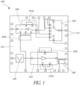
- FIG. 1 is a schematic diagram of one embodiment of a packaged module 100 for an RF communication system.
- the module 100 can contain multiple dies for processing (switching and amplifying) transmitted and received high frequency RF signals, particularly signals in the range of 1 GHz to 100 GHz, the module 100 may be referred to as a transmit/receive (TR) module.
- TR transmit/receive
- the module can be configured to accommodate differential packaging preferences for the different dies and enable the user to mount a single module on a system board.
- Figure 1 is schematic and illustrates lateral locations of devices on an upper side of a package substrate 101 and leads 112 on a lower side of the package substrate 101.
- the module 100 includes the package substrate 101, a first die 102, a second die 103, a third die 104, a filter 105 (notch filter, in this example), and a directional coupler 106 on the upper side of the substrate 101.
- the package substrate 101 can comprise any suitable type of substrate for providing electrical and mechanical connections between dies and a system board. In some embodiments, the package substrate 101 may also enable formation of an air cavity in conjunction with a lid.
- the package substrate 101 examples include a laminate substrate (e.g ., a printed circuit board or PCB, substrate), a molded leadframe substrate, a ceramic substrate, etc.
- the first die 102 comprises a silicon-based die and may comprise, for example, a switching die that includes radio frequency (RF) switching circuitry.
- the first die 102 may comprise a silicon on insulator (SOI) substrate.
- SOI silicon on insulator
- the first die 102 may be flip-chip mounted on the package substrate 101, as shown in Figure 5 .
- the first die 102 can be flipped over such that an active surface of the die 102 faces the package substrate 101, and interconnects (e.g ., copper pillars, solder bumps, etc.) may be bonded or otherwise connected to corresponding lands of the package substrate 101.
- interconnects e.g ., copper pillars, solder bumps, etc.
- the first die 102 may be wire bonded to the package substrate 101, as shown in Figures 6 and 7A .
- the first die 102 can be separately packaged before mounting on the package substrate 101, as shown in Figures 8A and 9 .
- At least one of the second die 103 and the third die 104 comprises a compound semiconductor (e.g., Group III-V material) substrate such as, for example, GaN or GaAs.
- each of the second and third dies 103, 104 comprise amplifier dies.
- the second die 103 can include a power amplifier (PA) and the third die 104 can include a low noise amplifier (LNA), one or both of which can be formed in group III-V semiconductor substrates.
- one of the second die 103 and the third die 104 may comprise a silicon substrate, such as an SOI substrate.
- the first die 102 and the third die 104 comprise silicon-based dies and the second die 103 comprises the compound semiconductor substrate.
- Using a silicon substrate for the first die 102 (e.g., the switching die) while using compound semiconductor substrates for one or both of the second and third dies 103, 104 (e.g., the PA and the LNA) can provide advantageous electrical behavior for their respective functions.
- compound semiconductor materials e.g., GaN, GaAs, etc.
- SOI substrate for the first switching die 102 can provide better switching properties than a compound semiconductor substrate.
- the filter 105 can be formed in or on the package substrate 101.
- the filter 105 can comprise, for example, a strip line filter and/or a notch filter.
- the filter 105 can be configured to select which frequencies are transmitted from and/or received by the module 100.
- the directional coupler 106 can be configured to act as a power detector.
- the directional coupler 106 may sample or divert RF power from an RF signal path, allowing a detection circuit to convert the RF power to DC voltage, which can be simply measured to determine the amount of RF power is in the module. It may be beneficial to measure the RF power because, for example, it enables fault detections.
- the module 100 may include encapsulating compound (e.g., a mold compound, an underfill, an encapsulant, an anti-oxidization gel, etc.) protecting electrical connections between the first die 102 and the package substrate 101.
- the substrate 101 may comprise a dam, moat or a trench (see Figures 3 , 4 , 6 and 7A ) at least partially around the first die 102 to limit underfill bleeding (see Figure 2 ).
- the module 100 may include just sufficient space between the first die 102 and the second die 103 and/or the third die 104 on the substrate 101 to prevent the underfill from reaching the second and third dies 103, 104.
- the module 100 as illustrated in Figure 1 has a square shape having a first side, a second side opposite the first side, a third side perpendicular to the first and second side, and a fourth side opposite the third side.
- the module 100 can have any other suitable shape in other arrangements.
- a length of each of the first to fourth sides of the module 100 can be about 7 mm (e.g., in a range of 5.0 mm to 10.0 mm, more particularly 6.0 mm to 8.0 mm), providing a substrate surface area of about 49 mm 2 (e.g., in a range of 25 mm 2 to 100 mm 2 , more particularly 36 mm 2 to 65 mm 2 ).
- the shape and/or the substrate surface area may be varied.
- the lateral footprint of the module 100 may be relatively small, while incorporating different types of RF dies and their associated functionality.
- packaging the first, second, and third dies 102, 103, 104 within the same packaged module can be beneficial.
- a co-packaging arrangement can provide enhanced front-end integration for a variety of applications such as, for example, a radar system.
- one or more passive components 107a-107d e.g ., capacitors and/or resistors
- a radar system can be provided within a single package that can be readily mounted on a system board and simplify installation for vehicles.
- a user may mount the module 100 on a system board, occupying a relatively small footprint relative to individually mounted dies, in a single mounting operation, thus providing a system-in-package incorporating amplification and switching functionality for a transmit/receive (TR) module.
- TR transmit/receive
- FIG 2 is a schematic top plan view of the module 100 of Figure 1 in one embodiment.
- the module 100 can comprise an RF module that includes a package substrate 101 (e.g., a laminate), a first die 102 ( e.g ., a switching die), a second die 103 ( e.g ., a PA die), and a third die 104 ( e.g ., an LNA die.
- the module 100 can also include a lid (not shown, see Figures 4-9 ) that is attached to the substrate 101.
- components of Figure 2 are the same as or generally similar to like-numbered components shown in Figure 1 .
- the module 100 includes encapsulating material (e.g., underfill 108) at least a portion between the substrate 101 and the first die 102 which is flip-chip bonded to the substrate 101.
- the underfill 108 can provide mechanical support for the first die 102 in addition to protecting the electrical connections from corrosion and ensuring electrical isolation.
- the encapsulating material (e.g., underfill 108) may result in bleedout 109, in some embodiments.
- an area or a space 110 can be provided on the substrate 101 between the first die 102 and the second and third dies 103, 104 that may prevent and/or mitigate the bleeding 109 from reaching the second and the third dies 103,104.
- the substrate 101 may have an encapsulant flow limiter, such as a dam, moat or trench (see Figures 3 , 4 , 6 and 7 ), to contain the bleedout 109.
- Figure 3 shows a schematic diagram of the module 100 for an RF communication system that includes an encapsulant flow limiter disposed around the first die 102.
- the encapsulant flow limiter that comprises a moat 111 is a closed shape surrounding the first die 102.
- the moat 111 can define a trench or recess defined in the surface of the substrate 101 around the first die 102.
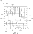
- Figure 4 shows a schematic diagram of the module 100 for an RF communication system that includes an encapsulant flow limiter, in this case in the form of a moat 111, disposed only partially around the first die 102, between the first die 102 and the second and third dies 103, 104.
- Figures 3 and 4 are schematic and illustrate locations of the devices on the upper side of the substrate 101 and leads 112 on the lower side of the package substrate 101.
- components of Figures 3 and 4 are the same as or generally similar to like-numbered components shown in Figures 1-2 .
- the moat 111 of Figures 3 and 4 can prevent and/or minimize the risk of the underfill 108 from reaching other components (particularly the second and third dies 103, 104) on the substrate 101.
- the first die 102 may be flip-chip mounted or wire bonded to the substrate 101.
- the underfill may be provided about the first die 102.
- an overmold encapsulant or an anti-oxidization gel may be provided on bond pads of the first die 102 to prevent oxidation of the bond pads.
- the module 100 with the moat 111 on the substrate 101 may have a space or the area 110 between the first die 102 and the second and third dies 103, 104 which may beneficially be smaller than the module 100 without the moat 111, such as the module 100 shown in Figures 1 and 2 .
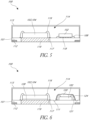
- Figure 5 is a cross sectional side view of the module 100 in one embodiment.
- the illustrated module 100 in Figure 5 includes the first die 102 flip-chip mounted on the substrate 101, the second die 103 and/or the third die 104 wire bonded to contact pads 117 of the substrate 101 by wires 116, and a package lid 113 attached to the substrate 101.
- the contact pads 117 may be embedded in the substrate 101.
- components of Figure 5 are the same as or generally similar to like-numbered components shown in Figures 1-4 .
- the second and/or third die 103, 104 may be mechanically mounted to the substrate 101 by die attach epoxy.
- the electrical connections between the first die 102 and the substrate can be protected by an encapsulating material.
- underfill 108 may be disposed between the package substrate 101 and the flip-chipped first die 102, e.g ., around the interconnects that connect the die 102 to the package substrate 101.
- No encapsulating material is provided on the second die and/or third die 103, 104, in some embodiments. Omitting the encapsulating material can reduce dielectric loss (e.g., lower loss tangent ⁇ ) for dies formed with III-V materials, such as amplifiers for RF signals.
- the substrate 101 and the lid 113 can define an air cavity 114 such that the devices (e.g., the first die 102 and/or the third die 104) mounted on the substrate 101 can be disposed in the cavity 114.
- the devices e.g., the first die 102 and/or the third die 104 mounted on the substrate 101 can be disposed in the cavity 114.
- electrical connections between the first die 102 and the substrate 101 can be protected and insulated with molding material, such as underfill 108, and the encapsulated first die 102 can be disposed in the cavity 114.
- the package lid 113 can be connected to the substrate 101, for example, by an adhesive.
- a metal slug 119 e.g., a solid piece of metal larger than a conventional via
- a copper slug can be integrated into the package substrate 101 beneath and preferably thermally contacting the second die 103 and/or the third die 104 (e.g., a PA die), thereby enhancing thermal performance.
- the metal slug may be formed beneath and preferably contacting the second die 103, the third die 104 and/or any other devices mounted on the substrate 101.
- the second die 103 may create more heat than the third die 104 during operation.
- metal slug 119 is explained with respect to Figure 5 and show in Figures 5, 6 and 8A , in connection with the second or third die 103, 104 that is wire bonded to the substrate 101, a similar metal slug may be provided to the second or third die 103, 104 that is attached to the substrate 101 by TSVs as shown in Figures 7A (with an air cavity) and 7B (without an air cavity), and/or to the first die 102 of various embodiments disclosed herein.
- the metal slug 119 may be used with package-in-package arrangements shown, for example, in Figures 8A and 9 , or in any embodiments that includes any die that may produce heat.
- Figure 6 is a cross sectional side view of the module 100 in one embodiment.
- the illustrated module 100 in Figure 6 includes the first die 102 wire bonded to contact pads 121 of the substrate 101 by wires 124, the second die 103 and/or the third die 104 wire bonded to contact pads 117 of the substrate 101 by wires 116, and a lid 113 attached to the substrate 101.
- the contact pads 117 and 121 may be embedded in the substrate 101.
- components of Figure 6 are the same as or generally similar to like-numbered components shown in Figures 1-5 .
- the first die 102 illustrated in Figure 6 is wire bonded to contact pads 121 of the substrate 101 by bond wires 124.
- the first die 102 when the first die 102 is wire bonded to the package substrate 101 as in Figure 6 , the first die 102 can comprise bond pads for receiving bond wires 124.
- the bond pads for the first die 102 when the first die comprises a silicon-based die, can comprise aluminum or copper.
- an encapsulation material e.g., an anti-oxidation gel 120
- Bond pads for silicon-based dies are often formed from aluminum. The encapsulating material may also protect the bond wires 124, as shown.
- the package substrate 101 illustrated in Figure 6 may include a moat 111 configured to limit the encroachment of the anti-oxidation gel 120 and/or any encapsulating material applied thereof.
- the module 100 may include a ground plane 128.
- the second and/or third die 103, 104 may be connected to a ground plane 128, which may be a part of the second and/or third die 103, 104 and formed at the wafer level, and/or may be formed as part of the package substrate 101.
- the ground plane 128 may be embedded in the package substrate 101.
- the ground plane 128 may be patterned as shown as a ground plane 132 in Figure 7A to permit signal lines to pass therethrough without shorting to ground.
- Figure 7A is a cross sectional side view of the module 100 in one embodiment. Unless otherwise noted, components of Figure 7A are the same as or generally similar to like-numbered components shown in Figures 1-6 . Unlike the embodiment of Figure 6 , the second and/or third die 103, 104 is bonded to the package substrate 101 without bond wires.
- the second and/or third dies 103, 104 can be mounted with the active side facing up (open to the air cavity 114) and can be electrically and mechanically connected to the package substrate 101, such as using solder or anisotropic conductive film, by way of through substrate vias (TSVs) 130 configured for carrying high frequency RF signals from the active side (e.g., a top surface) of the die(s) 103, 104 to the backside (e.g., a bottom surface) of the die(s) 103, 104.
- TSVs 130 that carry high frequency RF signals may also be referred to as RF vias.
- the TSVs 130 may comprise cylindrical holes with conductive material at least lining, and in some embodiments filling, a through-substrate hole.
- the vias may be formed by, for example, a monolithic microwave integrated circuit (MMIC) fabrication process.
- MMIC monolithic microwave integrated circuit
- the TSVs 130 are configured to carry RF signal connections and one or more ground connections configured to be electrically connected to corresponding pads 134 on the package substrate 101. Such embodiments can be beneficial in reducing the horizontal dimensions of the module 100 compared to embodiments with wire bonds. Attaching a die using the TSVs may also provide a better thermal performance than flip-chip mounting the die.
- Figure 7A also illustrates a ground plane 132 on the bottom of the second and/or third die 103, 104, where the ground plane 132 is patterned to allow signal line TSVs 130 to pass through the ground plane, whereas ground TSVs 130 may contact the ground plane 132.
- the embodiment of Figure 7A advantageously enables even smaller packages for the mixed technology module, which may serve as a transmit/receive module.
- the substrate surface area of the module 100 of Figure 7A may occupy between about 12 mm 2 and 65 mm 2 , more particularly between about 15 mm 2 and 50 mm 2 , while still providing the performance demanded of high frequency RF communication modules.
- ground plane 128 and the ground plane 132 are shown in Figure 6 in connection with the second or third die 103, 104 that is wire bonded to the substrate 101 and in Figure 7A in connection with the second or third die 103, 104 that is bonded via the RF vias, a similar ground plane may be provided to the first die 102 of various embodiments disclosed herein.
- the ground plane 128 and the ground plane 132 may be applied to embodiments without the air cavity, such as the embodiment shown in Figure 7B .
- the ground plane 128 and the ground plane 132 may be applied to package-in-package arrangements shown, for example, in Figures 8A and 9 , or in any embodiments that attaches any die to the substrate 101.
- the ground plane may be formed as part of the dies and/or the package substrates in various embodiments, and may be patterned to allow signal lines to pass therethrough without shorting.
- the module 100 may have one or more solder mask webs on the upper side of the package substrate 101.
- the package substrate 101 can comprise a plurality of pads that are spaced at least in part by the one or more solder masks.
- the solder mask webs may create an uneven surface on the upper side of the package substrate 101 such that a surface area of the upper side is made larger than the upper side without the solder mask webs.
- the solder mask webbed structure can enhance the adhesion between one or more of the dies and the package substrate 101 by way of intervening die attach materials (such as epoxy), preventing and/or mitigating delamination of the die(s).
- the package substrate 101 illustrated in Figure 7A also includes a dam 126 configured to limit flow of the anti-oxidation gel 120 and/or any encapsulating material applied thereof from reaching the other components on the package substrate 101.
- the package substrate 101 can have a through laminate vias 136 for providing heat and/or ground connections.
- the through-laminate vias 136 may each comprise a hole with metal disposed on a cylindrical wall. In some embodiments, the hole may be lined with metal. In other embodiments, the hole may be filled with metal. In some embodiments, the through-laminate vias 136 are configured to act both a thermal conduit and a ground connection.
- such the through-laminate vias 136 can serve as both a thermal conduit and a signal connection. It should be understood that the through-laminate vias 136 may be disposed at any location in the package substrate 101 with any embodiments disclosed herein.
- FIG 7B is a cross sectional side view of the module 100 in one embodiment. Unless otherwise noted, components of Figure 7B are the same as or generally similar to like-numbered components shown in Figures 1-7A .
- the module 100 includes the first die 102 that is flip-chip mounted to the substrate 101 and the second and/or third die 103, 104 mounted to the substrate 101 by TSVs.
- the first die 102 and the second and/or third die 103, 104 are embedded in an encapsulation compound 144.
- a single encapsulation compound 144 commonly encapsulates both a compound semiconductor die (such as the second and/or third die 103, 104) and a silicon-based die (such as the first die 102).
- the encapsulant 144 may be may be applied to a common laminate substrate prior to singulation of modules from one another, resulting in flush side edges from the package substrate 101 and the encapsulant 144.
- the first die 102 and the second and/or third die 103, 104 may be separately encapsulated, in which case the different encapsulation portions may comprise different material suitable for encapsulating the die.
- the encapsulation compound 144 can provide a mechanical protection. Such protection may provide reliability benefits. With improvements in the compound semiconductor technologies, negative effects of having the encapsulation compound 144 over Group III-V material dies may be minimized. With such improvement, users may choose to have the encapsulation compound 144 for its benefits despite its negative effects.
- Figure 7B benefits from use of RF vias in the form of TSVs 130, which allow strong thermal performance while handling RF frequency signals therethrough, and which is further improved by use of through-laminate vias 136.
- Use of molded encapsulant enables even further reduction on occupied footprint of the module 100, relative to modules employing wire bonding.
- Figure 8A is a cross sectional side view of the module 100 comprising a package-in-package in one embodiment.
- the module 100 includes an integrated circuit (IC) package 138 attached to the package substrate 101 by solder balls 142, the second and/or third die 103, 104 wire bonded to contact pads 117 of the package substrate 101 by wires 116, and a lid 113 attached to the package substrate 101.
- the second and/or third die 103, 104 is mechanically attached to the substrate 101 by an adhesive (e.g., die attach epoxy 154).
- an adhesive e.g., die attach epoxy 154
- the package 138 is illustrated with the first die 102 wire bonded to a package carrier 140 (e.g., lead frame, laminate substrate, etc).
- the first die 102 may be packaged separately from the module 100 prior to mounting on the package substrate 101.
- the first die 102 can be encapsulated, e.g., overmolded, in an encapsulation compound 144, and leads (e.g., solder balls 142 and/or lead frame leads) can be provided in the package carrier 140 for electrically and mechanically connecting the package 138 to the package substrate 101.
- leads e.g., solder balls 142 and/or lead frame leads
- the die(s) within the IC package 138 including encapsulation can be silicon-based dies, whereas die(s) exposed to the air cavity 114 can be Group III-V material dies.
- the first die 102 encapsulated within the IC package 138 is a silicon-based die that includes both LNA circuits and RF switch circuits.
- the second die 103 is mounted with its active surface exposed to the air cavity, and the first die 102 provides both LNA and RF switch functions for the TR module 100, such that a separate LNA die and separate packaging therefore can be omitted. Omitting the separate LNA die may allow for designing the module with smaller lateral footprint than that with the separate LNA die.
- the first die 102 for each of Figures 5-7 can be a silicon-based (e.g., SOI) die including LNA and RF switch circuitry, and a separate third die 104 can be omitted.
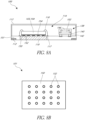
- Figure 8B is a top down plan view of a portion of the substrate 101 of Figure 8A that the second and/or third die 103, 104 is mounted, prior to mounting the second or third die 103, 104.
- the portion of the substrate 101 can include a solder mask 150.
- an adhesive e.g., a die attach epoxy 154
- the die attach epoxy 154 has better adhesion with the solder mask 150 than with the metal slug 119 or the ground plane 128 (see, for example, Figure 6 ) formed on the substrate 101.
- the solder mask 150 may reduce the chance of delamination of the die 103, 105 from the substrate 101.
- the solder mask 150 may have a webbed structure.
- the solder mask 150 may include a plurality of holes 152 that form the webbed structure. Such embodiments may provide increased surface area for better adhesion between the die attach epoxy 154 and the solder mask 150.
- the solder mask webs may create an uneven surface on the upper side of the package substrate 101 such that a surface area of the upper side is made larger than the upper side without the solder mask webs.
- the holes 152 may completely go through the solder mask 150 as shown in Figure 8B . In other embodiments, the holes 152 may be blind holes.
- solder mask 150 is shown in Figure 8A in connection with the second or third die 103, 104 that is wire bonded to the substrate 101
- a similar solder mask web may be provided to the second or third die 103, 104 that is attached to the substrate 101 by TSVs as shown in Figures 7A (with an air cavity) and 7B (without an air cavity), and/or to the first die 102 of various embodiments disclosed herein.
- the solder mask structure may be applied to package-in-package arrangements shown, for example, in Figures 8A and 9 , or in any embodiments that attaches any die to the substrate 101.
- the package substrate 101 can comprise a plurality of pads that are spaced at least in part by the one or more solder masks that form the webbed structure.
- Figure 9 is a cross sectional side view of the module 100 comprising a package-in-package in another embodiment.
- the module 100 includes an integrated circuit (IC) package 146 attached to the package substrate 101 by solder balls 142, the second die 103 wire bonded to contact pads 117 of the package substrate 101 by wires 116, and a lid 113 attached to the package substrate 101.
- IC integrated circuit
- components of Figure 9 are the same as or generally similar to like-numbered components shown in Figures 1-8B .
- the IC package 146 can comprise the first die 102 and the third die 104. As illustrated in Figure 9 , the third die 104 may be stacked on top of the first die 102.
- the dies 102, 104 may be packaged together separately from the module 100 and the IC package 146 can be mounted on the package substrate 101.
- the die(s) within the IC package 146 including encapsulation can be silicon-based dies, whereas die(s) exposed to the air cavity 114 can be Group III-V material dies.
- having the first die and the third die 102, 104 in the IC package 146 may reduce the lateral footprint of the module 100.
- the module 100 may include a die pad 148 that can serve as a ground and/or thermal connection between the package substrate 101 and the second die 103 that is attached to the substrate by wires 116.
- the module 100 may include array of through laminate vias 136 beneath the layer 148 for providing heat and/or ground connections.
- dams, moats, heat slugs, through-substrate vias and through-laminate vias of some illustrated embodiments can be exchanged for corresponding features in other illustrated embodiments.
- scope of the present invention herein disclosed should not be limited by the particular disclosed embodiments described above, but should be determined only by a fair reading of the claims that follow.
Landscapes
- Engineering & Computer Science (AREA)
- Power Engineering (AREA)
- Microelectronics & Electronic Packaging (AREA)
- Structures Or Materials For Encapsulating Or Coating Semiconductor Devices Or Solid State Devices (AREA)
- Chemical & Material Sciences (AREA)
- Dispersion Chemistry (AREA)
- Structures For Mounting Electric Components On Printed Circuit Boards (AREA)
Abstract
Description
- The field relates to radio frequency (RF) communication systems.
- A radio frequency (RF) communication system communicates by wirelessly transmitting and/or receiving RF signals. An RF communication system can include switches used for controlling access of various components to an antenna. Furthermore, an RF communication system can include amplifiers for providing amplification to RF signals. For high performance RF communications systems, particularly ones designed for high frequency and rugged applications, such as radar for critical applications, the different components have different structures and behavior. For example, some high performance parts are provided using III-V semiconductor substrates and other exotic materials, whereas other parts are provided in silicon or silicon-on-insulator (SOI) substrates. Such components typically communicate with one another through the system board. There remains a need for improved RF communication systems.
-
-
Figure 1 is a schematic diagram of one embodiment of a packaged module for a mixed technology RF communication system that illustrates lateral locations of devices on an upper side of a package substrate and leads on a lower side of the package substrate. -
Figure 2 is a schematic top plan view of the module ofFigure 1 in one embodiment that shows an underfill bleedout. -
Figure 3 shows a schematic diagram of the module for an RF communication system that includes an encapsulant flow limiter disposed around the first die. -
Figure 4 shows a schematic diagram of the module for an RF communication system that includes an encapsulant flow limiter disposed partially around the first die. -
Figure 5 is a cross sectional side view of the module in one embodiment that includes a flip-chip mounted die and a wire bonded die. -
Figure 6 is a cross sectional side view of the module in one embodiment that includes two wire bonded dies, one of which is provided with an encapsulating material and a dam. -
Figure 7A is a cross sectional side view of the module in one embodiment that includes a wire bonded die and a die with through substrate RF vias. -
Figure 7B is a cross sectional side view of the module in one embodiment that includes two encapsulated dies. -
Figure 8A is a cross sectional side view of the module in one embodiment that includes a separately packaged die and a wire bonded die. -
Figure 8B is a top down plan view of a portion of a substrate ofFigure 8A that the wire bonded die is mounted, prior to mounting the die. -
Figure 9 is a cross sectional side view of the module in one embodiment that includes a multi-die package and a wire bonded die. - In one aspect, a packaged radio frequency (RF) module is disclosed. The packaged RF module includes a package substrate, a first die, a second die, and an encapsulating material. The first die and the second die are electrically and mechanically attached to the package substrate. The first die comprises an RF switch and the second die comprises an RF amplifier. An encapsulating material protects electrical connections between the first die and the package substrate. The packaged RF module also includes a lid that is attached to the package substrate such that the package substrate and the lid at least partially define an air cavity within which the first and the second die are mounted. An active surface of the second die is exposed to the air cavity.
- In one embodiment, the first die is flip-chip attached to the package substrate by way of a plurality of interconnects between the first die and the package substrate. The encapsulating material comprises underfill that is disposed at least partially between the first die and the package substrate.
- In one embodiment, the packaged RF module further includes an encapsulant flow limiter on the package substrate at least partially around the first die and configured to capture encapsulating material bleeding from the first die.
- In one embodiment, the second die is connected to the package substrate by RF vias. The second die comprises a bottom surface opposite the active surface and the bottom surface comprises patterned contacts for RF signal connections between the second die and the package substrate.
- In one embodiment, the substrate includes one or more solder mask webs on the package substrate.
- In one embodiment, the substrate includes through substrate vias extending from a top surface of the substrate to a bottom surface of the package substrate. The through substrate vias can be configured to provide thermal or ground connections with the second die.
- In one embodiment, the first die is wire bonded to the package substrate and the encapsulating material comprises a gel at least over bond wire connections on the first die.
- In one embodiment, the first die is packaged within the encapsulating material and mounted onto the package substrate.
- In one embodiment, the packaged RF module further comprises a filter integrated with the package substrate. The filter can be integrated on a top surface of the substrate. The filter can be integrated in an internal layer of the package substrate.
- In one embodiment, the packaged RF module further comprises a metal slug integrated into the package substrate beneath the second die. The metal slug is configured to transfer heat from the second die. The metal slug can be configured to transfer heat from the second die and make a ground connection.
- In one embodiment, the packaged RF module further includes a third die that is attached to the package substrate and comprising a second RF amplifier. The second die can comprise a power amplifier (PA) and the third die can comprise a low noise amplifier (LNA). An active surface of the third die can be exposed to the air cavity.
- In one embodiment, the first die and the third die are packaged to define an integrated circuit (IC). The IC can be attached to the package substrate by solder balls.
- In one embodiment, the second die comprises a compound semiconductor substrate. The compound semiconductor substrate can comprise gallium nitride or gallium arsenide die.
- In one embodiment, the first die comprises a silicon-on-insulator (SOI) die.
- In another aspect, a transmit/receive (TR) module is disclosed. The TR module includes a package substrate, at least one compound semiconductor die and at least one silicon-based die. The dies are electrically and mechanically attached to the package substrate. The TR module also includes an encapsulating material that protects electrical connections between the silicon-based die and the package substrate. The TR module further includes a lid attached to the package substrate such that the package substrate and the lid at least partially define an air cavity within which the silicon-based and the compound semiconductor die are mounted. An active surface of the compound semiconductor die is exposed to the air cavity.
- In one embodiment, the compound semiconductor die comprises a Group III-V semiconductor substrate. The compound semiconductor die can comprise an amplifier die. The amplifier die can comprise a power amplifier. The silicon-based die can comprise an RF switch die. The TR module can further comprise a separate carrier substrate between the silicon-based die and the package substrate in a package-in-package arrangement.
- In one embodiment, the at least one silicon-based die comprises an low noise amplifier circuits and an RF switch circuit. The TR module can further comprise a separate carrier substrate between the silicon-based die and the package substrate in a package-in-package arrangement.
- In another aspect, a packaged radio frequency (RF) module is disclosed. The packaged PR module includes a package substrate, a compound semiconductor die and a silicon based die. The dies are mechanically attached to the package substrate. The compound semiconductor die is electrically connected to the package substrate by way of through substrate vias (TSVs) that are configured to carry RF signals. A silicon based die is electrically and mechanically attached to the package substrate. The package PF module also includes an encapsulating material that covers electrical connections of the silicon based die.
- In one embodiment, the compound semiconductor die is additionally encapsulated. The encapsulating material can cover the compound semiconductor die and the silicon based die.
- In one embodiment, the compound semiconductor die comprises an active surface facing away from the package substrate and a bottom surface opposite the active surface. The bottom surface can comprise patterned contacts for RF signal connections between the TSVs and the package substrate.
- Various embodiments disclosed herein may be particularly beneficial for high frequency systems, such as, for example, radar systems and wireless cellular communications systems (e.g., wireless systems conforming to the 5G standard). Embodiments disclosed herein may also be beneficial for packages that include multiple dies with different characteristics, e.g., dies that perform different functions, dies that have different operating parameters, etc. For example, some types of dies (e.g., amplifier dies) may benefit from packaging within an air cavity. Often such high performance dies are manufactured from compound semiconductor (e.g., Group III-IV) substrates. Other types of dies (e.g., switching dies) may benefit from isolation of packaging connections, which can be at least partially embedded in a molding compound. Switching dies for high performance applications can be manufactured from silicon or silicon-on-insulator (SOI) substrates (silicon-based substrates or dies), along with numerous other types of integrated circuit dies, including processor dies and some types of amplifier dies. Because of these different packaging preferences, typically such dies are separately packaged and communicate with one another through a system board.
- An RF communication system can include various types of switches and amplifiers. One type of amplifier is a low noise amplifier (LNA), which can provide amplification to relatively weak RF signals received by the system, while introducing only a relatively small amount of noise, thereby enhancing signal-to-noise ratio (SNR) and allowing the RF communication system to receive signals from greater distances and/or from relatively weak transmitters. For transmitting signals, a power amplifier (PA) can provide amplification for signals to be sent to the antenna, which can transmit the signals to an external device or system. A transmit/receive (TR) module as described herein can include either or both of an LNA and a PA.
- High performance amplifiers for high frequency and/or highly sensitive radar applications, can be manufactured (e.g., patterned or defined in an amplifier die) using gallium arsenide (GaAs), gallium nitride (GaN) or other compound semiconductor (particularly Group III-V) substrates. Compound semiconductor technologies offer good amplification characteristics and thus are suitable for fabricating RF amplifiers. In some embodiments, an LNA die can be provided with a group III-V semiconductor substrate. In some embodiments, a PA die can be provided with a group III-V semiconductor substrate. In some embodiments, at least one of the PA and LNA dies is provided with a silicon substrate and the other of the PA and LNA dies are provided with a group III-V semiconductor substrate. In some embodiments, both of the LNA and PA are formed in Group III-V substrates. An RF switch can be manufactured (e.g., patterned or defined in a switching die) using thinned silicon or silicon-on-insulator (SOI) technology.
- In various embodiments disclosed herein, the packaged RF module can comprise an air cavity package, in which integrated device dies may be disposed in an air cavity defined at least in part by a package substrate and a package lid attached to the package substrate. In some embodiments, some of the dies can be at least partially embedded in an encapsulating material. The encapsulating material can protect, for example, electrical connections and/or other portions of the die that utilize the molding material. However, the encapsulating material (which may comprise a plastic such as epoxy or other insulating material) may degrade the performance of group III-V dies (e.g., one or more high frequency amplifiers), which display superior performance when their active surfaces are exposed to air. For example, the encapsulating material can add capacitance, reduce gain, reduce power, etc. Accordingly, it can be beneficial to provide the amplifier die(s) (e.g., the LNA and/or PA dies) in an air cavity without the encapsulating material on its active surface in order to maintain high performance for the RF system.
- However, unlike for group III-V semiconductor dies, it may be beneficial to protect the electrical connections of silicon-based die(s) (e.g., a switching die) in an encapsulating material (e.g., overmold encapsulant, gel over wire bonds or underfill) regardless of whether the silicon-based die(s) are mounted to a substrate by a flip-chip technique or by a non-flip chip technique (e.g. by wire bonding). In a flip-chip technique, a die can be connected to the package substrate (e.g., a laminate or printed circuit board substrate in some arrangements) by way of conductive interconnects between the die and the substrate, for example, pillars (e.g., copper pillars), solder bumps, etc. that are bonded to the substrate. To reduce the chance of damaging the interconnects and/or the flip-chip die(s), and/or to provide support to the package, an underfill material can be provided around the interconnects underneath the flip-chip die(s). In non-flip chip techniques, for example, wire bonding techniques, a silicon-based die (such as a switching die) can be wire bonded to the package substrate. For example, a silicon-based switching die can have bond pads (e.g., aluminum or copper bond pads in some embodiments) to which bonding wires may be connected. To reduce risk of oxidation of the bond pads, the encapsulating material may be provided over the switching die(s), the wire bonds, and unbonded portions of the bond pads. Silicon-based amplifiers can be similarly packaged with encapsulating material for more robust and protected connections.
-
Figure 1 is a schematic diagram of one embodiment of a packagedmodule 100 for an RF communication system. Because themodule 100 can contain multiple dies for processing (switching and amplifying) transmitted and received high frequency RF signals, particularly signals in the range of 1 GHz to 100 GHz, themodule 100 may be referred to as a transmit/receive (TR) module. Advantageously, despite including dies of mixed technology, including both III-V and silicon-based dies, the module can be configured to accommodate differential packaging preferences for the different dies and enable the user to mount a single module on a system board. -
Figure 1 is schematic and illustrates lateral locations of devices on an upper side of apackage substrate 101 and leads 112 on a lower side of thepackage substrate 101. Themodule 100 includes thepackage substrate 101, afirst die 102, asecond die 103, athird die 104, a filter 105 (notch filter, in this example), and adirectional coupler 106 on the upper side of thesubstrate 101. Thepackage substrate 101 can comprise any suitable type of substrate for providing electrical and mechanical connections between dies and a system board. In some embodiments, thepackage substrate 101 may also enable formation of an air cavity in conjunction with a lid. Examples of thepackage substrate 101 include a laminate substrate (e.g., a printed circuit board or PCB, substrate), a molded leadframe substrate, a ceramic substrate, etc. Thefirst die 102 comprises a silicon-based die and may comprise, for example, a switching die that includes radio frequency (RF) switching circuitry. Thefirst die 102 may comprise a silicon on insulator (SOI) substrate. In some embodiments, thefirst die 102 may be flip-chip mounted on thepackage substrate 101, as shown inFigure 5 . In such embodiments, thefirst die 102 can be flipped over such that an active surface of the die 102 faces thepackage substrate 101, and interconnects (e.g., copper pillars, solder bumps, etc.) may be bonded or otherwise connected to corresponding lands of thepackage substrate 101. In some other embodiments, thefirst die 102 may be wire bonded to thepackage substrate 101, as shown inFigures 6 and7A . In still other embodiments, thefirst die 102 can be separately packaged before mounting on thepackage substrate 101, as shown inFigures 8A and9 . - At least one of the
second die 103 and thethird die 104 comprises a compound semiconductor (e.g., Group III-V material) substrate such as, for example, GaN or GaAs. In some embodiments, each of the second and third dies 103, 104 comprise amplifier dies. For example, thesecond die 103 can include a power amplifier (PA) and thethird die 104 can include a low noise amplifier (LNA), one or both of which can be formed in group III-V semiconductor substrates. In some embodiments, one of thesecond die 103 and thethird die 104 may comprise a silicon substrate, such as an SOI substrate. In some embodiments, thefirst die 102 and thethird die 104 comprise silicon-based dies and thesecond die 103 comprises the compound semiconductor substrate. - Using a silicon substrate for the first die 102 (e.g., the switching die) while using compound semiconductor substrates for one or both of the second and third dies 103, 104 (e.g., the PA and the LNA) can provide advantageous electrical behavior for their respective functions. For example, using compound semiconductor materials (e.g., GaN, GaAs, etc.) for one or both of the second and third amplifier dies 103, 104 can provide better amplification properties than silicon-based dies. By contrast, using an SOI substrate for the first switching die 102 can provide better switching properties than a compound semiconductor substrate.
- In some embodiments, the
filter 105 can be formed in or on thepackage substrate 101. In some embodiments, thefilter 105 can comprise, for example, a strip line filter and/or a notch filter. Thefilter 105 can be configured to select which frequencies are transmitted from and/or received by themodule 100. Thedirectional coupler 106 can be configured to act as a power detector. Thedirectional coupler 106 may sample or divert RF power from an RF signal path, allowing a detection circuit to convert the RF power to DC voltage, which can be simply measured to determine the amount of RF power is in the module. It may be beneficial to measure the RF power because, for example, it enables fault detections. - The
module 100 may include encapsulating compound (e.g., a mold compound, an underfill, an encapsulant, an anti-oxidization gel, etc.) protecting electrical connections between thefirst die 102 and thepackage substrate 101. In some embodiments, where underfill is used for thefirst die 102 or any other flip-chip die, thesubstrate 101 may comprise a dam, moat or a trench (seeFigures 3 ,4 ,6 and7A ) at least partially around thefirst die 102 to limit underfill bleeding (seeFigure 2 ). In some embodiments, themodule 100 may include just sufficient space between thefirst die 102 and thesecond die 103 and/or thethird die 104 on thesubstrate 101 to prevent the underfill from reaching the second and third dies 103, 104. - The
module 100 as illustrated inFigure 1 has a square shape having a first side, a second side opposite the first side, a third side perpendicular to the first and second side, and a fourth side opposite the third side. Themodule 100 can have any other suitable shape in other arrangements. A length of each of the first to fourth sides of themodule 100 can be about 7 mm (e.g., in a range of 5.0 mm to 10.0 mm, more particularly 6.0 mm to 8.0 mm), providing a substrate surface area of about 49 mm2 (e.g., in a range of 25 mm2 to 100 mm2, more particularly 36 mm2 to 65 mm2). However, skilled artisan would understand that, in some embodiments, the shape and/or the substrate surface area may be varied. Beneficially, the lateral footprint of themodule 100 may be relatively small, while incorporating different types of RF dies and their associated functionality. - In some embodiments, packaging the first, second, and third dies 102, 103, 104 (e.g., a switch, a PA and an LNA) within the same packaged module can be beneficial. For example, such a co-packaging arrangement can provide enhanced front-end integration for a variety of applications such as, for example, a radar system. In some embodiments, one or more
passive components 107a-107d (e.g., capacitors and/or resistors) may be surface mounted on thesubstrate 101. Accordingly, a radar system can be provided within a single package that can be readily mounted on a system board and simplify installation for vehicles. Accordingly, a user may mount themodule 100 on a system board, occupying a relatively small footprint relative to individually mounted dies, in a single mounting operation, thus providing a system-in-package incorporating amplification and switching functionality for a transmit/receive (TR) module. -
Figure 2 is a schematic top plan view of themodule 100 ofFigure 1 in one embodiment. Themodule 100 can comprise an RF module that includes a package substrate 101 (e.g., a laminate), a first die 102 (e.g., a switching die), a second die 103 (e.g., a PA die), and a third die 104 (e.g., an LNA die. Themodule 100 can also include a lid (not shown, seeFigures 4-9 ) that is attached to thesubstrate 101. Unless otherwise noted, components ofFigure 2 are the same as or generally similar to like-numbered components shown inFigure 1 . - The
module 100 includes encapsulating material (e.g., underfill 108) at least a portion between thesubstrate 101 and thefirst die 102 which is flip-chip bonded to thesubstrate 101. Theunderfill 108 can provide mechanical support for thefirst die 102 in addition to protecting the electrical connections from corrosion and ensuring electrical isolation. - As illustrated in
Figure 2 , the encapsulating material (e.g., underfill 108) may result inbleedout 109, in some embodiments. As also illustrated inFigure 2 , an area or aspace 110 can be provided on thesubstrate 101 between thefirst die 102 and the second and third dies 103, 104 that may prevent and/or mitigate the bleeding 109 from reaching the second and the third dies 103,104. Additionally or alternatively, thesubstrate 101 may have an encapsulant flow limiter, such as a dam, moat or trench (seeFigures 3 ,4 ,6 and7 ), to contain thebleedout 109. -
Figure 3 shows a schematic diagram of themodule 100 for an RF communication system that includes an encapsulant flow limiter disposed around thefirst die 102. In the illustrated embodiment, the encapsulant flow limiter that comprises amoat 111 is a closed shape surrounding thefirst die 102. Themoat 111 can define a trench or recess defined in the surface of thesubstrate 101 around thefirst die 102. -
Figure 4 shows a schematic diagram of themodule 100 for an RF communication system that includes an encapsulant flow limiter, in this case in the form of amoat 111, disposed only partially around thefirst die 102, between thefirst die 102 and the second and third dies 103, 104.Figures 3 and4 are schematic and illustrate locations of the devices on the upper side of thesubstrate 101 and leads 112 on the lower side of thepackage substrate 101. Unless otherwise noted, components ofFigures 3 and4 are the same as or generally similar to like-numbered components shown inFigures 1-2 . Beneficially, themoat 111 ofFigures 3 and4 can prevent and/or minimize the risk of theunderfill 108 from reaching other components (particularly the second and third dies 103, 104) on thesubstrate 101. - In some embodiments, the
first die 102 may be flip-chip mounted or wire bonded to thesubstrate 101. When thefirst die 102 is flip-chip mounted on thesubstrate 101, the underfill may be provided about thefirst die 102. When thefirst die 102 is wire bonded to thesubstrate 102, an overmold encapsulant or an anti-oxidization gel may be provided on bond pads of thefirst die 102 to prevent oxidation of the bond pads. In some embodiments, themodule 100 with themoat 111 on thesubstrate 101 may have a space or thearea 110 between thefirst die 102 and the second and third dies 103, 104 which may beneficially be smaller than themodule 100 without themoat 111, such as themodule 100 shown inFigures 1 and2 . -
Figure 5 is a cross sectional side view of themodule 100 in one embodiment. The illustratedmodule 100 inFigure 5 includes thefirst die 102 flip-chip mounted on thesubstrate 101, thesecond die 103 and/or thethird die 104 wire bonded to contactpads 117 of thesubstrate 101 bywires 116, and apackage lid 113 attached to thesubstrate 101. Thecontact pads 117 may be embedded in thesubstrate 101. Unless otherwise noted, components ofFigure 5 are the same as or generally similar to like-numbered components shown inFigures 1-4 . In some embodiments, when thesecond die 103 and/or thethird die 104 are electrically connected to thesubstrate 101 by way of wire bonding as shown inFigure 5 , the second and/orthird die substrate 101 by die attach epoxy. In some embodiments, when thefirst die 102 is flip-chip mounted on thepackage substrate 101 as inFigure 5 , the electrical connections between thefirst die 102 and the substrate can be protected by an encapsulating material. In some embodiments, underfill 108 may be disposed between thepackage substrate 101 and the flip-chippedfirst die 102, e.g., around the interconnects that connect thedie 102 to thepackage substrate 101. No encapsulating material is provided on the second die and/orthird die Figure 5 , thesubstrate 101 and thelid 113 can define anair cavity 114 such that the devices (e.g., thefirst die 102 and/or the third die 104) mounted on thesubstrate 101 can be disposed in thecavity 114. In such embodiments, electrical connections between thefirst die 102 and thesubstrate 101 can be protected and insulated with molding material, such asunderfill 108, and the encapsulated first die 102 can be disposed in thecavity 114. Thepackage lid 113 can be connected to thesubstrate 101, for example, by an adhesive. - In some embodiments, as in
Figure 5 , a metal slug 119 (e.g., a solid piece of metal larger than a conventional via), such as, for example, a copper slug, can be integrated into thepackage substrate 101 beneath and preferably thermally contacting thesecond die 103 and/or the third die 104 (e.g., a PA die), thereby enhancing thermal performance. In some embodiments, the metal slug may be formed beneath and preferably contacting thesecond die 103, thethird die 104 and/or any other devices mounted on thesubstrate 101. In some embodiments, thesecond die 103 may create more heat than thethird die 104 during operation. - Though the
metal slug 119 is explained with respect toFigure 5 and show inFigures 5, 6 and8A , in connection with the second orthird die substrate 101, a similar metal slug may be provided to the second orthird die substrate 101 by TSVs as shown inFigures 7A (with an air cavity) and 7B (without an air cavity), and/or to thefirst die 102 of various embodiments disclosed herein. Themetal slug 119 may be used with package-in-package arrangements shown, for example, inFigures 8A and9 , or in any embodiments that includes any die that may produce heat. -
Figure 6 is a cross sectional side view of themodule 100 in one embodiment. The illustratedmodule 100 inFigure 6 includes thefirst die 102 wire bonded to contactpads 121 of thesubstrate 101 bywires 124, thesecond die 103 and/or thethird die 104 wire bonded to contactpads 117 of thesubstrate 101 bywires 116, and alid 113 attached to thesubstrate 101. Thecontact pads substrate 101. Unless otherwise noted, components ofFigure 6 are the same as or generally similar to like-numbered components shown inFigures 1-5 . Unlike the embodiment ofFigure 5 , thefirst die 102 illustrated inFigure 6 is wire bonded to contactpads 121 of thesubstrate 101 bybond wires 124. In some embodiments, when thefirst die 102 is wire bonded to thepackage substrate 101 as inFigure 6 , thefirst die 102 can comprise bond pads for receivingbond wires 124. In some embodiments, when the first die comprises a silicon-based die, the bond pads for thefirst die 102 can comprise aluminum or copper. In such embodiments, an encapsulation material (e.g., an anti-oxidation gel 120) may be disposed over at least a portion of thefirst die 102 to protect the bond pads on thefirst die 102 from corrosion. Bond pads for silicon-based dies are often formed from aluminum. The encapsulating material may also protect thebond wires 124, as shown. - The
package substrate 101 illustrated inFigure 6 may include amoat 111 configured to limit the encroachment of theanti-oxidation gel 120 and/or any encapsulating material applied thereof. Themodule 100 may include aground plane 128. In some embodiments, the second and/orthird die ground plane 128, which may be a part of the second and/orthird die package substrate 101. In some embodiments, theground plane 128 may be embedded in thepackage substrate 101. In some embodiments, theground plane 128 may be patterned as shown as aground plane 132 inFigure 7A to permit signal lines to pass therethrough without shorting to ground. -
Figure 7A is a cross sectional side view of themodule 100 in one embodiment. Unless otherwise noted, components ofFigure 7A are the same as or generally similar to like-numbered components shown inFigures 1-6 . Unlike the embodiment ofFigure 6 , the second and/orthird die package substrate 101 without bond wires. For example, the second and/or third dies 103, 104 can be mounted with the active side facing up (open to the air cavity 114) and can be electrically and mechanically connected to thepackage substrate 101, such as using solder or anisotropic conductive film, by way of through substrate vias (TSVs) 130 configured for carrying high frequency RF signals from the active side (e.g., a top surface) of the die(s) 103, 104 to the backside (e.g., a bottom surface) of the die(s) 103, 104. TheTSVs 130 that carry high frequency RF signals may also be referred to as RF vias. TheTSVs 130 may comprise cylindrical holes with conductive material at least lining, and in some embodiments filling, a through-substrate hole. The vias may be formed by, for example, a monolithic microwave integrated circuit (MMIC) fabrication process. TheTSVs 130 are configured to carry RF signal connections and one or more ground connections configured to be electrically connected to correspondingpads 134 on thepackage substrate 101. Such embodiments can be beneficial in reducing the horizontal dimensions of themodule 100 compared to embodiments with wire bonds. Attaching a die using the TSVs may also provide a better thermal performance than flip-chip mounting the die.Figure 7A also illustrates aground plane 132 on the bottom of the second and/orthird die ground plane 132 is patterned to allowsignal line TSVs 130 to pass through the ground plane, whereasground TSVs 130 may contact theground plane 132. - By obviating wire bonds, the use of RF vias in the form of
TSVs 130, the embodiment ofFigure 7A advantageously enables even smaller packages for the mixed technology module, which may serve as a transmit/receive module. For example, the substrate surface area of themodule 100 ofFigure 7A may occupy between about 12 mm2 and 65 mm2, more particularly between about 15 mm2 and 50 mm2, while still providing the performance demanded of high frequency RF communication modules. - Though the
ground plane 128 and theground plane 132 are shown inFigure 6 in connection with the second orthird die substrate 101 and inFigure 7A in connection with the second orthird die first die 102 of various embodiments disclosed herein. In some embodiments, theground plane 128 and theground plane 132 may be applied to embodiments without the air cavity, such as the embodiment shown inFigure 7B . Theground plane 128 and theground plane 132 may be applied to package-in-package arrangements shown, for example, inFigures 8A and9 , or in any embodiments that attaches any die to thesubstrate 101. As noted above, the ground plane may be formed as part of the dies and/or the package substrates in various embodiments, and may be patterned to allow signal lines to pass therethrough without shorting. - As illustrated with respect to the embodiment below of
Figures 8A and 8B , in some embodiments, themodule 100 may have one or more solder mask webs on the upper side of thepackage substrate 101. For example, thepackage substrate 101 can comprise a plurality of pads that are spaced at least in part by the one or more solder masks. In some embodiments, the solder mask webs may create an uneven surface on the upper side of thepackage substrate 101 such that a surface area of the upper side is made larger than the upper side without the solder mask webs. In some embodiments, the solder mask webbed structure can enhance the adhesion between one or more of the dies and thepackage substrate 101 by way of intervening die attach materials (such as epoxy), preventing and/or mitigating delamination of the die(s). - The
package substrate 101 illustrated inFigure 7A also includes adam 126 configured to limit flow of theanti-oxidation gel 120 and/or any encapsulating material applied thereof from reaching the other components on thepackage substrate 101. In some embodiments, thepackage substrate 101 can have a throughlaminate vias 136 for providing heat and/or ground connections. In some embodiments, the through-laminate vias 136 may each comprise a hole with metal disposed on a cylindrical wall. In some embodiments, the hole may be lined with metal. In other embodiments, the hole may be filled with metal. In some embodiments, the through-laminate vias 136 are configured to act both a thermal conduit and a ground connection. In other embodiments, such the through-laminate vias 136 can serve as both a thermal conduit and a signal connection. It should be understood that the through-laminate vias 136 may be disposed at any location in thepackage substrate 101 with any embodiments disclosed herein. -
Figure 7B is a cross sectional side view of themodule 100 in one embodiment. Unless otherwise noted, components ofFigure 7B are the same as or generally similar to like-numbered components shown inFigures 1-7A . Themodule 100 includes thefirst die 102 that is flip-chip mounted to thesubstrate 101 and the second and/orthird die substrate 101 by TSVs. Thefirst die 102 and the second and/orthird die encapsulation compound 144. In the illustrated embodiment, asingle encapsulation compound 144 commonly encapsulates both a compound semiconductor die (such as the second and/orthird die 103, 104) and a silicon-based die (such as the first die 102). Theencapsulant 144 may be may be applied to a common laminate substrate prior to singulation of modules from one another, resulting in flush side edges from thepackage substrate 101 and theencapsulant 144. In other embodiments, thefirst die 102 and the second and/orthird die - The
encapsulation compound 144 can provide a mechanical protection. Such protection may provide reliability benefits. With improvements in the compound semiconductor technologies, negative effects of having theencapsulation compound 144 over Group III-V material dies may be minimized. With such improvement, users may choose to have theencapsulation compound 144 for its benefits despite its negative effects. - Like
Figure 7A , the embodiment ofFigure 7B benefits from use of RF vias in the form ofTSVs 130, which allow strong thermal performance while handling RF frequency signals therethrough, and which is further improved by use of through-laminate vias 136. Use of molded encapsulant enables even further reduction on occupied footprint of themodule 100, relative to modules employing wire bonding. -
Figure 8A is a cross sectional side view of themodule 100 comprising a package-in-package in one embodiment. Themodule 100 includes an integrated circuit (IC)package 138 attached to thepackage substrate 101 bysolder balls 142, the second and/orthird die pads 117 of thepackage substrate 101 bywires 116, and alid 113 attached to thepackage substrate 101. The second and/orthird die substrate 101 by an adhesive (e.g., die attach epoxy 154). Unless otherwise noted, components ofFigure 8A are the same as or generally similar to like-numbered components shown inFigures 1-7B . Thepackage 138 is illustrated with thefirst die 102 wire bonded to a package carrier 140 (e.g., lead frame, laminate substrate, etc). In some embodiments, thefirst die 102 may be packaged separately from themodule 100 prior to mounting on thepackage substrate 101. For example, thefirst die 102 can be encapsulated, e.g., overmolded, in anencapsulation compound 144, and leads (e.g.,solder balls 142 and/or lead frame leads) can be provided in thepackage carrier 140 for electrically and mechanically connecting thepackage 138 to thepackage substrate 101. While thefirst die 102 is illustrated as separately packaged, the skilled artisan will appreciate that other dies can additionally or alternatively be packaged for mounting on thepackage substrate 101. The die(s) within theIC package 138 including encapsulation can be silicon-based dies, whereas die(s) exposed to theair cavity 114 can be Group III-V material dies. - In one embodiment, the
first die 102 encapsulated within theIC package 138 is a silicon-based die that includes both LNA circuits and RF switch circuits. In such an embodiment, thesecond die 103 is mounted with its active surface exposed to the air cavity, and thefirst die 102 provides both LNA and RF switch functions for theTR module 100, such that a separate LNA die and separate packaging therefore can be omitted. Omitting the separate LNA die may allow for designing the module with smaller lateral footprint than that with the separate LNA die. The skilled artisan will appreciate that, similarly, thefirst die 102 for each ofFigures 5-7 can be a silicon-based (e.g., SOI) die including LNA and RF switch circuitry, and a separatethird die 104 can be omitted. -
Figure 8B is a top down plan view of a portion of thesubstrate 101 ofFigure 8A that the second and/orthird die third die substrate 101 can include asolder mask 150. When attaching the second and/orthird die substrate 101, an adhesive (e.g., a die attach epoxy 154) may be applied between a bottom surface of the second and/orthird die substrate 101. In some embodiments, the die attachepoxy 154 has better adhesion with thesolder mask 150 than with themetal slug 119 or the ground plane 128 (see, for example,Figure 6 ) formed on thesubstrate 101. Therefore, the solder mask may reduce the chance of delamination of thedie substrate 101. In some embodiments, thesolder mask 150 may have a webbed structure. In some embodiments, thesolder mask 150 may include a plurality ofholes 152 that form the webbed structure. Such embodiments may provide increased surface area for better adhesion between the die attachepoxy 154 and thesolder mask 150. In some embodiments, the solder mask webs may create an uneven surface on the upper side of thepackage substrate 101 such that a surface area of the upper side is made larger than the upper side without the solder mask webs. In some embodiments, theholes 152 may completely go through thesolder mask 150 as shown inFigure 8B . In other embodiments, theholes 152 may be blind holes. - Though the
solder mask 150 is shown inFigure 8A in connection with the second orthird die substrate 101, a similar solder mask web may be provided to the second orthird die substrate 101 by TSVs as shown inFigures 7A (with an air cavity) and 7B (without an air cavity), and/or to thefirst die 102 of various embodiments disclosed herein. The solder mask structure may be applied to package-in-package arrangements shown, for example, inFigures 8A and9 , or in any embodiments that attaches any die to thesubstrate 101. In some embodiments, thepackage substrate 101 can comprise a plurality of pads that are spaced at least in part by the one or more solder masks that form the webbed structure. -
Figure 9 is a cross sectional side view of themodule 100 comprising a package-in-package in another embodiment. Themodule 100 includes an integrated circuit (IC)package 146 attached to thepackage substrate 101 bysolder balls 142, thesecond die 103 wire bonded to contactpads 117 of thepackage substrate 101 bywires 116, and alid 113 attached to thepackage substrate 101. Unless otherwise noted, components ofFigure 9 are the same as or generally similar to like-numbered components shown inFigures 1-8B . TheIC package 146 can comprise thefirst die 102 and thethird die 104. As illustrated inFigure 9 , thethird die 104 may be stacked on top of thefirst die 102. For example, the dies 102, 104 may be packaged together separately from themodule 100 and theIC package 146 can be mounted on thepackage substrate 101. The die(s) within theIC package 146 including encapsulation can be silicon-based dies, whereas die(s) exposed to theair cavity 114 can be Group III-V material dies. In some embodiments, having the first die and thethird die IC package 146 may reduce the lateral footprint of themodule 100. - The
module 100 may include adie pad 148 that can serve as a ground and/or thermal connection between thepackage substrate 101 and thesecond die 103 that is attached to the substrate bywires 116. Themodule 100 may include array of throughlaminate vias 136 beneath thelayer 148 for providing heat and/or ground connections. - Although this invention has been disclosed in the context of certain embodiments and examples, it will be understood by those skilled in the art that the present invention extends beyond the specifically disclosed embodiments to other alternative embodiments and/or uses of the invention and obvious modifications and equivalents thereof. In addition, while several variations of the invention have been shown and described in detail, other modifications, which are within the scope of this invention, will be readily apparent to those of skill in the art based upon this disclosure. It is also contemplated that various combinations or sub-combinations of the specific features and aspects of the embodiments may be made and still fall within the scope of the invention. It should be understood that various features and aspects of the disclosed embodiments can be combined with, or substituted for, one another in order to form varying modes of the disclosed invention. For example, the dams, moats, heat slugs, through-substrate vias and through-laminate vias of some illustrated embodiments can be exchanged for corresponding features in other illustrated embodiments. Thus, it is intended that the scope of the present invention herein disclosed should not be limited by the particular disclosed embodiments described above, but should be determined only by a fair reading of the claims that follow.
- By way of non-limiting example, some aspects of the disclosure are set out in the following numbered clauses.
- 1. A packaged radio frequency (RF) module comprising:
- a package substrate;
- a first die electrically and mechanically attached to the package substrate, the first die comprising an RF switch;
- a second die electrically and mechanically attached to the package substrate, the second die comprising an RF amplifier;
- an encapsulating material protecting electrical connections between the first die and the package substrate; and
- a lid attached to the package substrate such that the package substrate and the lid at least partially define an air cavity within which the first and the second die are mounted, an active surface of the second die being exposed to the air cavity.
- 2. The packaged RF module of clause 1, wherein the first die is flip-chip attached to the package substrate by way of a plurality of interconnects between the first die and the package substrate.
- 3. The packaged RF module of clause 2, wherein the encapsulating material comprises underfill disposed at least partially between the first die and the package substrate.
- 4. The packaged RF module of clause 1, further comprising an encapsulant flow limiter on the package substrate at least partially around the first die and configured to capture encapsulating material bleeding from the first die.
- 5. The packaged RF module of clause 1, wherein the second die is connected to the package substrate by RF vias.
- 6. The packaged RF module of clause 1, wherein the second die comprises a bottom surface opposite the active surface, the bottom surface comprises patterned contacts for RF signal connections between the second die and the package substrate.
- 7. The packaged RF module of clause 1, wherein at least one of the following applies:
- the substrate comprises one or more solder webs on the package substrate;
- the substrate comprises through substrate vias extending from a top surface of the substrate to a bottom surface of the package substrate, the through substrate vias configured to provide thermal or ground connections with the second die;
- the first die is wire bonded to the package substrate, wherein the encapsulating material comprises a gel at least over bond wired connections on the first die; and
- the first die is packaged within the encapsulating material and mounted onto the package substrate.
- 8. The packaged RF module of clause 1, further comprising a filter integrated with the package substrate, wherein the filter is preferably integrated on a top surface of the substrate or in an internal layer of the package substrate.
- 9. The packaged RF module of clause 1, further comprising a metal slug integrated into the package substrate beneath the second die, wherein the metal slug is configured to transfer heat from the second die and/or make a ground connection.
- 10. The packaged RF module of clause 1, further comprising a third die attached to the package substrate and comprising a second RF amplifier.
- 11. The packaged RF module of clause 10, wherein the second die comprises a power amplifier (PA) and the third die comprises a low noise amplifier (LNA).
- 12. The packaged RF module of clause 11, wherein an active surface of the third die is exposed to the air cavity.
- 13. The packaged RF module of clause 10, wherein the first die and the third die are packaged to define an integrated circuit (IC), the IC is attached to the package substrate by solder balls.
- 14. The packaged RF module of clause 1, wherein the second die comprises a compound semiconductor substrate, wherein the compound semiconductor substrate preferably comprises gallium nitride or gallium arsenide die.
- 15. The packaged RF module of clause 1, wherein the first die comprises a silicon-on-insulator (SOI) die.
Claims (15)
- A packaged radio frequency (RF) module comprising:a package substrate;a first die electrically and mechanically attached to the package substrate, the first die comprising an RF switch, wherein the first die is flip-chip attached to the package substrate by way of a plurality of interconnects between the first die and the package substrate;a second die electrically and mechanically attached to the package substrate, the second die comprising an RF amplifier;an encapsulating material protecting electrical connections between the first die and the package substrate; anda lid attached to the package substrate such that the package substrate and the lid at least partially define an air cavity within which the first and the second die are mounted, an active surface of the second die being exposed to the air cavity.
- The packaged RF module of Claim 1, wherein the encapsulating material comprises underfill disposed at least partially between the first die and the package substrate.
- The packaged RF module of Claim 1 or Claim 2, further comprising an encapsulant flow limiter on the package substrate at least partially around the first die and configured to capture encapsulating material bleeding from the first die.
- The packaged RF module of Claim 1, wherein the second die is connected to the package substrate by RF vias.
- The packaged RF module of Claim 1, wherein the second die comprises a bottom surface opposite the active surface, the bottom surface comprises patterned contacts for RF signal connections between the second die and the package substrate.
- The packaged RF module of Claim 1, wherein at least one of the following applies:the substrate comprises one or more solder webs on the package substrate; andthe substrate comprises through substrate vias extending from a top surface of the substrate to a bottom surface of the package substrate, the through substrate vias configured to provide thermal or ground connections with the second die.
- The packaged RF module of Claim 1, further comprising a filter integrated with the package substrate, wherein the filter is preferably integrated on a top surface of the substrate or in an internal layer of the package substrate.
- The packaged RF module of Claim 1, further comprising a metal slug integrated into the package substrate beneath the second die, wherein the metal slug is configured to transfer heat from the second die and/or make a ground connection.
- The packaged RF module of Claim 1, further comprising a third die attached to the package substrate and comprising a second RF amplifier.
- The packaged RF module of Claim 9, wherein the second die comprises a power amplifier (PA) and the third die comprises a low noise amplifier (LNA).
- The packaged RF module of Claim 10, wherein an active surface of the third die is exposed to the air cavity.
- The packaged RF module of Claim 9, wherein the first die and the third die are packaged to define an integrated circuit (IC), the IC is attached to the package substrate by solder balls.
- The packaged RF module of Claim 1, wherein the second die comprises a compound semiconductor substrate, wherein the compound semiconductor substrate preferably comprises gallium nitride or gallium arsenide die.
- The packaged RF module of Claim 1, wherein the first die comprises a silicon-on-insulator (SOI) die.
- The packaged RF module of any preceding claim, wherein the second die is electrically connected to the package substrate by of through substrate vias, TSVs, configured to carry RF signals from an active side of the second die to a backside of the second die.
Applications Claiming Priority (3)
| Application Number | Priority Date | Filing Date | Title |
|---|---|---|---|
| US201862659590P | 2018-04-18 | 2018-04-18 | |
| US15/969,483 US10510694B2 (en) | 2018-04-18 | 2018-05-02 | Radio frequency communication systems |
| EP19168589.0A EP3557613B1 (en) | 2018-04-18 | 2019-04-11 | Radio frequency module |
Related Parent Applications (2)
| Application Number | Title | Priority Date | Filing Date |
|---|---|---|---|
| EP19168589.0A Division EP3557613B1 (en) | 2018-04-18 | 2019-04-11 | Radio frequency module |
| EP19168589.0A Division-Into EP3557613B1 (en) | 2018-04-18 | 2019-04-11 | Radio frequency module |
Publications (2)
| Publication Number | Publication Date |
|---|---|
| EP4258336A2 true EP4258336A2 (en) | 2023-10-11 |
| EP4258336A3 EP4258336A3 (en) | 2024-08-14 |
Family
ID=66379689
Family Applications (2)
| Application Number | Title | Priority Date | Filing Date |
|---|---|---|---|
| EP19168589.0A Active EP3557613B1 (en) | 2018-04-18 | 2019-04-11 | Radio frequency module |
| EP23192886.2A Pending EP4258336A3 (en) | 2018-04-18 | 2019-04-11 | Radio frequency module |
Family Applications Before (1)
| Application Number | Title | Priority Date | Filing Date |
|---|---|---|---|
| EP19168589.0A Active EP3557613B1 (en) | 2018-04-18 | 2019-04-11 | Radio frequency module |
Country Status (2)
| Country | Link |
|---|---|
| US (1) | US10510694B2 (en) |
| EP (2) | EP3557613B1 (en) |
Families Citing this family (14)
| Publication number | Priority date | Publication date | Assignee | Title |
|---|---|---|---|---|
| JP2020126921A (en) * | 2019-02-04 | 2020-08-20 | 株式会社村田製作所 | High-frequency module and communication device |
| US11887937B2 (en) * | 2019-02-08 | 2024-01-30 | Ams International Ag | Reduction in susceptibility of analog integrated circuits and sensors to radio frequency interference |
| US10923438B2 (en) | 2019-04-26 | 2021-02-16 | Taiwan Semiconductor Manufacturing Co., Ltd. | Package structure and method for forming the same |
| JP2021158554A (en) * | 2020-03-27 | 2021-10-07 | 株式会社村田製作所 | High-frequency module and communication device |
| JP2021158556A (en) * | 2020-03-27 | 2021-10-07 | 株式会社村田製作所 | High-frequency module and communication device |
| JP2021164022A (en) | 2020-03-31 | 2021-10-11 | 株式会社村田製作所 | High-frequency module and communication device |
| JP2021164017A (en) | 2020-03-31 | 2021-10-11 | 株式会社村田製作所 | High frequency module and communication equipment |
| KR102378171B1 (en) * | 2020-08-12 | 2022-03-25 | 제엠제코(주) | Coupled semiconductor package |
| US11877505B2 (en) * | 2020-10-15 | 2024-01-16 | Qorvo Us, Inc. | Fluorinated polymers with low dielectric loss for environmental protection in semiconductor devices |
| CN112332788B (en) * | 2020-10-22 | 2024-07-02 | 浙江三维利普维网络有限公司 | Radio frequency power amplifier module |
| US11742302B2 (en) * | 2020-10-23 | 2023-08-29 | Wolfspeed, Inc. | Electronic device packages with internal moisture barriers |
| WO2022124230A1 (en) * | 2020-12-11 | 2022-06-16 | 株式会社村田製作所 | Integrated circuit and high frequency module |
| US11784613B2 (en) * | 2021-03-26 | 2023-10-10 | Wolfspeed, Inc. | High output power density radio frequency transistor amplifiers in flat no-lead overmold packages |
| JP7708643B2 (en) * | 2021-10-29 | 2025-07-15 | 新光電気工業株式会社 | Wiring board, semiconductor device, and method for manufacturing wiring board |
Family Cites Families (38)
| Publication number | Priority date | Publication date | Assignee | Title |
|---|---|---|---|---|
| JP2002118487A (en) * | 2000-10-06 | 2002-04-19 | Matsushita Electric Ind Co Ltd | High frequency composite switch module |
| JP3937840B2 (en) * | 2002-01-10 | 2007-06-27 | 株式会社日立製作所 | High frequency module |
| US7307331B2 (en) * | 2004-03-31 | 2007-12-11 | Intel Corporation | Integrated radio front-end module with embedded circuit elements |
| US7692295B2 (en) * | 2006-03-31 | 2010-04-06 | Intel Corporation | Single package wireless communication device |
| US7557421B1 (en) | 2006-07-20 | 2009-07-07 | Rf Micro Devices, Inc. | Hybrid radio frequency integrated circuit using gallium nitride epitaxy layers grown on a donor substrate |
| TW200905759A (en) * | 2007-07-20 | 2009-02-01 | Azurewave Technologies Inc | Through-hole structure for a wafer level packaging |
| US7508267B1 (en) | 2007-09-28 | 2009-03-24 | Rockwell Collins, Inc. | GaN based digital controlled broadband MMIC power amplifier |
| JP5239309B2 (en) * | 2007-11-21 | 2013-07-17 | 株式会社村田製作所 | Semiconductor device |
| US7833895B2 (en) * | 2008-05-12 | 2010-11-16 | Texas Instruments Incorporated | TSVS having chemically exposed TSV tips for integrated circuit devices |
| KR101481577B1 (en) * | 2008-09-29 | 2015-01-13 | 삼성전자주식회사 | Semiconductor package having dam of ink jet method and manufacturing method thereof |
| JP5407667B2 (en) * | 2008-11-05 | 2014-02-05 | 株式会社村田製作所 | Semiconductor device |
| JP5324191B2 (en) * | 2008-11-07 | 2013-10-23 | ルネサスエレクトロニクス株式会社 | Semiconductor device |
| US8829999B2 (en) | 2010-05-20 | 2014-09-09 | Cree, Inc. | Low noise amplifiers including group III nitride based high electron mobility transistors |
| US8576010B2 (en) | 2010-10-19 | 2013-11-05 | Samsung Electronics Co., Ltd. | Apparatus and method for a switched capacitor architecture for multi-band doherty power amplifiers |
| CN103430447A (en) | 2011-01-11 | 2013-12-04 | 航空网络公司 | Systems and methods for a radio frequency transmitter with improved linearity and power out utilizing pre-distortion and a GAN (gallium nitride) power amplifier device |
| US9667206B2 (en) | 2011-02-24 | 2017-05-30 | Dsp Group Ltd. | Linear row array integrated power combiner for RF power amplifiers |
| US8665022B2 (en) | 2011-04-28 | 2014-03-04 | Rf Micro Devices, Inc. | Low noise-linear power distributed amplifier |
| JP5765174B2 (en) * | 2011-09-30 | 2015-08-19 | 富士通株式会社 | Electronic equipment |
| CN102611393B (en) | 2011-12-26 | 2014-12-24 | 深圳市虹远通信有限责任公司 | Radio frequency power amplifier system having waveband switching function |
| JP5512740B2 (en) * | 2012-05-11 | 2014-06-04 | シャープ株式会社 | High frequency circuit and high frequency module having the same |
| US9196958B2 (en) * | 2012-07-26 | 2015-11-24 | Apple Inc. | Antenna structures and shield layers on packaged wireless circuits |
| US9312820B2 (en) | 2012-09-23 | 2016-04-12 | Dsp Group Ltd. | CMOS based TX/RX switch |
| TWI511257B (en) * | 2013-07-30 | 2015-12-01 | 國立交通大學 | Connection structure of semiconductor components |
| US9472859B2 (en) * | 2014-05-20 | 2016-10-18 | International Business Machines Corporation | Integration of area efficient antennas for phased array or wafer scale array antenna applications |
| US9515645B2 (en) | 2014-06-03 | 2016-12-06 | Infineon Technologies Ag | System and method for a radio frequency switch |
| US9537605B1 (en) | 2014-07-22 | 2017-01-03 | Bae Systems Information And Electronic Systems Integration Inc. | Ultra-wideband high-power solid-state transmitter for electronic warfare applications |
| US9960145B2 (en) * | 2015-03-25 | 2018-05-01 | Qorvo Us, Inc. | Flip chip module with enhanced properties |
| US9806678B2 (en) | 2015-06-29 | 2017-10-31 | Eridan Communications, Inc. | Bootstrap class-D wideband RF power amplifier |
| US10594355B2 (en) | 2015-06-30 | 2020-03-17 | Skyworks Solutions, Inc. | Devices and methods related to radio-frequency filters on silicon-on-insulator substrate |
| US10003451B2 (en) | 2015-10-08 | 2018-06-19 | Macom Technology Solutions Holdings, Inc. | Dual-input, high power handling, power combining LNA for full duplex communications systems |
| US11335651B2 (en) | 2015-12-22 | 2022-05-17 | Intel Corporation | Microelectronic devices designed with compound semiconductor devices and integrated on an inter die fabric |
| CN105789163A (en) * | 2016-03-23 | 2016-07-20 | 宜确半导体(苏州)有限公司 | Radio frequency front-end chip integration module and radio frequency front-end chip integration method |
| US10158419B2 (en) | 2016-04-27 | 2018-12-18 | Facebook, Inc. | Wireless communication utilizing post-amplification carrier aggregation |
| US10171053B2 (en) | 2016-05-05 | 2019-01-01 | Skyworks Solutions, Inc. | Apparatus and methods for power amplifiers with an injection-locked oscillator driver stage |
| US9742445B1 (en) | 2016-07-01 | 2017-08-22 | Bae Systems Information And Electronic Systems Integration Inc. | High power radio frequency amplifier architecture |
| US20180048305A1 (en) * | 2016-08-09 | 2018-02-15 | Skyworks Solutions, Inc. | Radio-frequency switch with switchable capacitor |
| CN106374855B (en) | 2016-08-26 | 2019-06-14 | 宜确半导体(苏州)有限公司 | A kind of radio-frequency power amplifier module and RF front-end module |
| US10109903B2 (en) * | 2016-10-06 | 2018-10-23 | Invensas Corporation | Flipped RF filters and components |
-
2018
- 2018-05-02 US US15/969,483 patent/US10510694B2/en active Active
-
2019
- 2019-04-11 EP EP19168589.0A patent/EP3557613B1/en active Active
- 2019-04-11 EP EP23192886.2A patent/EP4258336A3/en active Pending
Also Published As
| Publication number | Publication date |
|---|---|
| EP4258336A3 (en) | 2024-08-14 |
| EP3557613B1 (en) | 2023-12-27 |
| US20190326234A1 (en) | 2019-10-24 |
| EP3557613A1 (en) | 2019-10-23 |
| US10510694B2 (en) | 2019-12-17 |
Similar Documents
| Publication | Publication Date | Title |
|---|---|---|
| US10510694B2 (en) | Radio frequency communication systems | |
| EP3413347B1 (en) | Semiconductor package having discrete antenna device | |
| US7078264B2 (en) | Stacked semiconductor die | |
| US12094842B2 (en) | Semiconductor device having an antenna arranged over an active main surface of a semiconductor die | |
| US7843042B2 (en) | Wafer level integration package | |
| EP3745457B1 (en) | Semiconductor package having discrete antenna device | |
| US7928564B2 (en) | Multichip module package and fabrication method | |
| US7884460B2 (en) | Integrated circuit packaging system with carrier and method of manufacture thereof | |
| US20190103365A1 (en) | Selectively shielded semiconductor package | |
| JP2008543092A (en) | Apparatus and method for packaging an antenna for an integrated circuit chip for millimeter wave applications | |
| US12283555B2 (en) | Semiconductor packages | |
| US20150380343A1 (en) | Flip chip mmic having mounting stiffener | |
| US20220310471A1 (en) | Integrated circuit die stacked with backer die including capacitors and thermal vias | |
| US20180122777A1 (en) | Hybrid micro-circuit device with stacked chip components | |
| JP2000299427A (en) | High frequency integrated circuit device | |
| US9082738B2 (en) | Semiconductor package with improved thermal properties | |
| US7352056B2 (en) | Semiconductor package structure with microstrip antennan | |
| US6933603B2 (en) | Multi-substrate layer semiconductor packages and method for making same | |
| US10236270B2 (en) | Interposer and semiconductor module for use in automotive applications |
Legal Events
| Date | Code | Title | Description |
|---|---|---|---|
| PUAI | Public reference made under article 153(3) epc to a published international application that has entered the european phase |
Free format text: ORIGINAL CODE: 0009012 |
|
| STAA | Information on the status of an ep patent application or granted ep patent |
Free format text: STATUS: REQUEST FOR EXAMINATION WAS MADE |
|
| 17P | Request for examination filed |
Effective date: 20230823 |
|
| AC | Divisional application: reference to earlier application |
Ref document number: 3557613 Country of ref document: EP Kind code of ref document: P |
|
| AK | Designated contracting states |
Kind code of ref document: A2 Designated state(s): AL AT BE BG CH CY CZ DE DK EE ES FI FR GB GR HR HU IE IS IT LI LT LU LV MC MK MT NL NO PL PT RO RS SE SI SK SM TR |
|
| REG | Reference to a national code |
Ref country code: DE Ref legal event code: R079 Free format text: PREVIOUS MAIN CLASS: H01L0023000000 Ipc: H01L0023040000 |
|
| RIC1 | Information provided on ipc code assigned before grant |
Ipc: H01L 25/065 20230101ALN20240403BHEP Ipc: H01L 23/00 20060101ALI20240403BHEP Ipc: H01L 23/367 20060101ALI20240403BHEP Ipc: H01L 23/66 20060101ALI20240403BHEP Ipc: H01L 23/04 20060101AFI20240403BHEP |
|
| REG | Reference to a national code |
Ref country code: DE Ref legal event code: R079 Free format text: PREVIOUS MAIN CLASS: H01L0023040000 Ipc: H01L0023660000 |
|
| PUAL | Search report despatched |
Free format text: ORIGINAL CODE: 0009013 |
|
| AK | Designated contracting states |
Kind code of ref document: A3 Designated state(s): AL AT BE BG CH CY CZ DE DK EE ES FI FR GB GR HR HU IE IS IT LI LT LU LV MC MK MT NL NO PL PT RO RS SE SI SK SM TR |
|
| RIC1 | Information provided on ipc code assigned before grant |
Ipc: H01L 23/04 20060101ALN20240711BHEP Ipc: H01L 25/065 20230101ALN20240711BHEP Ipc: H01L 23/00 20060101ALI20240711BHEP Ipc: H01L 23/367 20060101ALI20240711BHEP Ipc: H01L 23/66 20060101AFI20240711BHEP |