EP4254529A1 - Perovskite solar cell module and manufacturing method for same - Google Patents
Perovskite solar cell module and manufacturing method for same Download PDFInfo
- Publication number
- EP4254529A1 EP4254529A1 EP21898327.8A EP21898327A EP4254529A1 EP 4254529 A1 EP4254529 A1 EP 4254529A1 EP 21898327 A EP21898327 A EP 21898327A EP 4254529 A1 EP4254529 A1 EP 4254529A1
- Authority
- EP
- European Patent Office
- Prior art keywords
- charge transport
- separated
- electrode
- layer
- transport layer
- Prior art date
- Legal status (The legal status is an assumption and is not a legal conclusion. Google has not performed a legal analysis and makes no representation as to the accuracy of the status listed.)
- Pending
Links
- 238000004519 manufacturing process Methods 0.000 title claims abstract description 18
- 239000000758 substrate Substances 0.000 claims abstract description 97
- 239000010410 layer Substances 0.000 claims description 750
- 239000002346 layers by function Substances 0.000 claims description 229
- 239000000463 material Substances 0.000 claims description 30
- QVGXLLKOCUKJST-UHFFFAOYSA-N atomic oxygen Chemical compound [O] QVGXLLKOCUKJST-UHFFFAOYSA-N 0.000 claims description 12
- 229910052760 oxygen Inorganic materials 0.000 claims description 12
- 239000001301 oxygen Substances 0.000 claims description 12
- 238000000059 patterning Methods 0.000 claims description 8
- 238000000034 method Methods 0.000 claims description 6
- 238000005530 etching Methods 0.000 claims description 4
- 238000006243 chemical reaction Methods 0.000 abstract description 4
- 239000013078 crystal Substances 0.000 abstract description 2
- 230000003287 optical effect Effects 0.000 abstract 1
- 239000000126 substance Substances 0.000 description 70
- 238000001312 dry etching Methods 0.000 description 69
- 238000012545 processing Methods 0.000 description 69
- 238000001039 wet etching Methods 0.000 description 69
- 230000000903 blocking effect Effects 0.000 description 15
- 230000005525 hole transport Effects 0.000 description 9
- 239000000460 chlorine Substances 0.000 description 8
- JKQOBWVOAYFWKG-UHFFFAOYSA-N molybdenum trioxide Chemical compound O=[Mo](=O)=O JKQOBWVOAYFWKG-UHFFFAOYSA-N 0.000 description 8
- XLOMVQKBTHCTTD-UHFFFAOYSA-N Zinc monoxide Chemical compound [Zn]=O XLOMVQKBTHCTTD-UHFFFAOYSA-N 0.000 description 6
- 239000011248 coating agent Substances 0.000 description 6
- 238000000576 coating method Methods 0.000 description 6
- 238000012986 modification Methods 0.000 description 6
- 230000004048 modification Effects 0.000 description 6
- 125000004429 atom Chemical group 0.000 description 5
- 229910052751 metal Inorganic materials 0.000 description 5
- 239000002184 metal Substances 0.000 description 5
- ZCYVEMRRCGMTRW-UHFFFAOYSA-N 7553-56-2 Chemical compound [I] ZCYVEMRRCGMTRW-UHFFFAOYSA-N 0.000 description 4
- XKRFYHLGVUSROY-UHFFFAOYSA-N Argon Chemical compound [Ar] XKRFYHLGVUSROY-UHFFFAOYSA-N 0.000 description 4
- IJGRMHOSHXDMSA-UHFFFAOYSA-N Atomic nitrogen Chemical compound N#N IJGRMHOSHXDMSA-UHFFFAOYSA-N 0.000 description 4
- WKBOTKDWSSQWDR-UHFFFAOYSA-N Bromine atom Chemical compound [Br] WKBOTKDWSSQWDR-UHFFFAOYSA-N 0.000 description 4
- OKTJSMMVPCPJKN-UHFFFAOYSA-N Carbon Chemical compound [C] OKTJSMMVPCPJKN-UHFFFAOYSA-N 0.000 description 4
- ZAMOUSCENKQFHK-UHFFFAOYSA-N Chlorine atom Chemical compound [Cl] ZAMOUSCENKQFHK-UHFFFAOYSA-N 0.000 description 4
- 239000004642 Polyimide Substances 0.000 description 4
- GDTBXPJZTBHREO-UHFFFAOYSA-N bromine Substances BrBr GDTBXPJZTBHREO-UHFFFAOYSA-N 0.000 description 4
- 229910052794 bromium Inorganic materials 0.000 description 4
- 229910052801 chlorine Inorganic materials 0.000 description 4
- 239000010949 copper Substances 0.000 description 4
- JAONJTDQXUSBGG-UHFFFAOYSA-N dialuminum;dizinc;oxygen(2-) Chemical compound [O-2].[O-2].[O-2].[O-2].[O-2].[Al+3].[Al+3].[Zn+2].[Zn+2] JAONJTDQXUSBGG-UHFFFAOYSA-N 0.000 description 4
- 239000010931 gold Substances 0.000 description 4
- 229910052740 iodine Inorganic materials 0.000 description 4
- 239000011630 iodine Substances 0.000 description 4
- -1 polyethylene terephthalate Polymers 0.000 description 4
- 229920000139 polyethylene terephthalate Polymers 0.000 description 4
- 239000005020 polyethylene terephthalate Substances 0.000 description 4
- 229920001721 polyimide Polymers 0.000 description 4
- 239000011669 selenium Substances 0.000 description 4
- 229910052782 aluminium Inorganic materials 0.000 description 3
- 229910052799 carbon Inorganic materials 0.000 description 3
- 229910052802 copper Inorganic materials 0.000 description 3
- 238000010008 shearing Methods 0.000 description 3
- 229910052709 silver Inorganic materials 0.000 description 3
- 238000007764 slot die coating Methods 0.000 description 3
- 238000004528 spin coating Methods 0.000 description 3
- 238000005507 spraying Methods 0.000 description 3
- 238000002207 thermal evaporation Methods 0.000 description 3
- XOLBLPGZBRYERU-UHFFFAOYSA-N tin dioxide Chemical compound O=[Sn]=O XOLBLPGZBRYERU-UHFFFAOYSA-N 0.000 description 3
- 239000011787 zinc oxide Substances 0.000 description 3
- RYGMFSIKBFXOCR-UHFFFAOYSA-N Copper Chemical compound [Cu] RYGMFSIKBFXOCR-UHFFFAOYSA-N 0.000 description 2
- PXGOKWXKJXAPGV-UHFFFAOYSA-N Fluorine Chemical compound FF PXGOKWXKJXAPGV-UHFFFAOYSA-N 0.000 description 2
- UFHFLCQGNIYNRP-UHFFFAOYSA-N Hydrogen Chemical compound [H][H] UFHFLCQGNIYNRP-UHFFFAOYSA-N 0.000 description 2
- 229920000144 PEDOT:PSS Polymers 0.000 description 2
- OAICVXFJPJFONN-UHFFFAOYSA-N Phosphorus Chemical compound [P] OAICVXFJPJFONN-UHFFFAOYSA-N 0.000 description 2
- 229920012266 Poly(ether sulfone) PES Polymers 0.000 description 2
- BUGBHKTXTAQXES-UHFFFAOYSA-N Selenium Chemical compound [Se] BUGBHKTXTAQXES-UHFFFAOYSA-N 0.000 description 2
- BQCADISMDOOEFD-UHFFFAOYSA-N Silver Chemical compound [Ag] BQCADISMDOOEFD-UHFFFAOYSA-N 0.000 description 2
- NINIDFKCEFEMDL-UHFFFAOYSA-N Sulfur Chemical compound [S] NINIDFKCEFEMDL-UHFFFAOYSA-N 0.000 description 2
- GWEVSGVZZGPLCZ-UHFFFAOYSA-N Titan oxide Chemical compound O=[Ti]=O GWEVSGVZZGPLCZ-UHFFFAOYSA-N 0.000 description 2
- 229910021417 amorphous silicon Inorganic materials 0.000 description 2
- 229910052786 argon Inorganic materials 0.000 description 2
- 229910052789 astatine Inorganic materials 0.000 description 2
- RYXHOMYVWAEKHL-UHFFFAOYSA-N astatine atom Chemical compound [At] RYXHOMYVWAEKHL-UHFFFAOYSA-N 0.000 description 2
- 238000005229 chemical vapour deposition Methods 0.000 description 2
- IVMYJDGYRUAWML-UHFFFAOYSA-N cobalt(II) oxide Inorganic materials [Co]=O IVMYJDGYRUAWML-UHFFFAOYSA-N 0.000 description 2
- 229910021419 crystalline silicon Inorganic materials 0.000 description 2
- 230000005611 electricity Effects 0.000 description 2
- 229910052731 fluorine Inorganic materials 0.000 description 2
- 239000011737 fluorine Substances 0.000 description 2
- 239000011521 glass Substances 0.000 description 2
- 229910052737 gold Inorganic materials 0.000 description 2
- 125000005843 halogen group Chemical group 0.000 description 2
- 229910052739 hydrogen Inorganic materials 0.000 description 2
- 239000001257 hydrogen Substances 0.000 description 2
- 229910052743 krypton Inorganic materials 0.000 description 2
- DNNSSWSSYDEUBZ-UHFFFAOYSA-N krypton atom Chemical compound [Kr] DNNSSWSSYDEUBZ-UHFFFAOYSA-N 0.000 description 2
- 239000007769 metal material Substances 0.000 description 2
- 239000000203 mixture Substances 0.000 description 2
- 229910052754 neon Inorganic materials 0.000 description 2
- GKAOGPIIYCISHV-UHFFFAOYSA-N neon atom Chemical compound [Ne] GKAOGPIIYCISHV-UHFFFAOYSA-N 0.000 description 2
- 229910052757 nitrogen Inorganic materials 0.000 description 2
- 229910052755 nonmetal Inorganic materials 0.000 description 2
- 150000002894 organic compounds Chemical class 0.000 description 2
- 230000035515 penetration Effects 0.000 description 2
- 229910052698 phosphorus Inorganic materials 0.000 description 2
- 239000011574 phosphorus Substances 0.000 description 2
- 239000011112 polyethylene naphthalate Substances 0.000 description 2
- 229910052704 radon Inorganic materials 0.000 description 2
- SYUHGPGVQRZVTB-UHFFFAOYSA-N radon atom Chemical compound [Rn] SYUHGPGVQRZVTB-UHFFFAOYSA-N 0.000 description 2
- 229910052711 selenium Inorganic materials 0.000 description 2
- 229910052717 sulfur Inorganic materials 0.000 description 2
- 239000011593 sulfur Substances 0.000 description 2
- ZNOKGRXACCSDPY-UHFFFAOYSA-N tungsten trioxide Chemical compound O=[W](=O)=O ZNOKGRXACCSDPY-UHFFFAOYSA-N 0.000 description 2
- 229910052724 xenon Inorganic materials 0.000 description 2
- FHNFHKCVQCLJFQ-UHFFFAOYSA-N xenon atom Chemical compound [Xe] FHNFHKCVQCLJFQ-UHFFFAOYSA-N 0.000 description 2
- PNKUSGQVOMIXLU-UHFFFAOYSA-N Formamidine Chemical compound NC=N PNKUSGQVOMIXLU-UHFFFAOYSA-N 0.000 description 1
- GYHNNYVSQQEPJS-UHFFFAOYSA-N Gallium Chemical compound [Ga] GYHNNYVSQQEPJS-UHFFFAOYSA-N 0.000 description 1
- XUIMIQQOPSSXEZ-UHFFFAOYSA-N Silicon Chemical compound [Si] XUIMIQQOPSSXEZ-UHFFFAOYSA-N 0.000 description 1
- 239000002042 Silver nanowire Substances 0.000 description 1
- XAGFODPZIPBFFR-UHFFFAOYSA-N aluminium Chemical compound [Al] XAGFODPZIPBFFR-UHFFFAOYSA-N 0.000 description 1
- 230000015556 catabolic process Effects 0.000 description 1
- 238000006731 degradation reaction Methods 0.000 description 1
- 230000006866 deterioration Effects 0.000 description 1
- 238000011161 development Methods 0.000 description 1
- FZHSXDYFFIMBIB-UHFFFAOYSA-L diiodolead;methanamine Chemical compound NC.I[Pb]I FZHSXDYFFIMBIB-UHFFFAOYSA-L 0.000 description 1
- 230000000694 effects Effects 0.000 description 1
- 238000003912 environmental pollution Methods 0.000 description 1
- 239000002803 fossil fuel Substances 0.000 description 1
- 229910052733 gallium Inorganic materials 0.000 description 1
- PCHJSUWPFVWCPO-UHFFFAOYSA-N gold Chemical compound [Au] PCHJSUWPFVWCPO-UHFFFAOYSA-N 0.000 description 1
- 229910021389 graphene Inorganic materials 0.000 description 1
- XMBWDFGMSWQBCA-UHFFFAOYSA-N hydrogen iodide Chemical compound I XMBWDFGMSWQBCA-UHFFFAOYSA-N 0.000 description 1
- 229910052738 indium Inorganic materials 0.000 description 1
- APFVFJFRJDLVQX-UHFFFAOYSA-N indium atom Chemical compound [In] APFVFJFRJDLVQX-UHFFFAOYSA-N 0.000 description 1
- PJXISJQVUVHSOJ-UHFFFAOYSA-N indium(III) oxide Inorganic materials [O-2].[O-2].[O-2].[In+3].[In+3] PJXISJQVUVHSOJ-UHFFFAOYSA-N 0.000 description 1
- AMGQUBHHOARCQH-UHFFFAOYSA-N indium;oxotin Chemical compound [In].[Sn]=O AMGQUBHHOARCQH-UHFFFAOYSA-N 0.000 description 1
- HRHKULZDDYWVBE-UHFFFAOYSA-N indium;oxozinc;tin Chemical compound [In].[Sn].[Zn]=O HRHKULZDDYWVBE-UHFFFAOYSA-N 0.000 description 1
- 238000004020 luminiscence type Methods 0.000 description 1
- GNRSAWUEBMWBQH-UHFFFAOYSA-N nickel(II) oxide Inorganic materials [Ni]=O GNRSAWUEBMWBQH-UHFFFAOYSA-N 0.000 description 1
- 239000012466 permeate Substances 0.000 description 1
- 238000010248 power generation Methods 0.000 description 1
- 239000004065 semiconductor Substances 0.000 description 1
- 229910052710 silicon Inorganic materials 0.000 description 1
- 239000010703 silicon Substances 0.000 description 1
- 239000004332 silver Substances 0.000 description 1
- 239000002356 single layer Substances 0.000 description 1
- 229910001887 tin oxide Inorganic materials 0.000 description 1
- YVTHLONGBIQYBO-UHFFFAOYSA-N zinc indium(3+) oxygen(2-) Chemical compound [O--].[Zn++].[In+3] YVTHLONGBIQYBO-UHFFFAOYSA-N 0.000 description 1
Images


Classifications
-
- H—ELECTRICITY
- H10—SEMICONDUCTOR DEVICES; ELECTRIC SOLID-STATE DEVICES NOT OTHERWISE PROVIDED FOR
- H10K—ORGANIC ELECTRIC SOLID-STATE DEVICES
- H10K30/00—Organic devices sensitive to infrared radiation, light, electromagnetic radiation of shorter wavelength or corpuscular radiation
- H10K30/80—Constructional details
-
- C—CHEMISTRY; METALLURGY
- C07—ORGANIC CHEMISTRY
- C07F—ACYCLIC, CARBOCYCLIC OR HETEROCYCLIC COMPOUNDS CONTAINING ELEMENTS OTHER THAN CARBON, HYDROGEN, HALOGEN, OXYGEN, NITROGEN, SULFUR, SELENIUM OR TELLURIUM
- C07F7/00—Compounds containing elements of Groups 4 or 14 of the Periodic System
- C07F7/24—Lead compounds
-
- H—ELECTRICITY
- H10—SEMICONDUCTOR DEVICES; ELECTRIC SOLID-STATE DEVICES NOT OTHERWISE PROVIDED FOR
- H10K—ORGANIC ELECTRIC SOLID-STATE DEVICES
- H10K30/00—Organic devices sensitive to infrared radiation, light, electromagnetic radiation of shorter wavelength or corpuscular radiation
- H10K30/10—Organic devices sensitive to infrared radiation, light, electromagnetic radiation of shorter wavelength or corpuscular radiation comprising heterojunctions between organic semiconductors and inorganic semiconductors
- H10K30/15—Sensitised wide-bandgap semiconductor devices, e.g. dye-sensitised TiO2
-
- H—ELECTRICITY
- H10—SEMICONDUCTOR DEVICES; ELECTRIC SOLID-STATE DEVICES NOT OTHERWISE PROVIDED FOR
- H10K—ORGANIC ELECTRIC SOLID-STATE DEVICES
- H10K39/00—Integrated devices, or assemblies of multiple devices, comprising at least one organic radiation-sensitive element covered by group H10K30/00
- H10K39/10—Organic photovoltaic [PV] modules; Arrays of single organic PV cells
- H10K39/12—Electrical configurations of PV cells, e.g. series connections or parallel connections
-
- H—ELECTRICITY
- H10—SEMICONDUCTOR DEVICES; ELECTRIC SOLID-STATE DEVICES NOT OTHERWISE PROVIDED FOR
- H10K—ORGANIC ELECTRIC SOLID-STATE DEVICES
- H10K85/00—Organic materials used in the body or electrodes of devices covered by this subclass
-
- H—ELECTRICITY
- H10—SEMICONDUCTOR DEVICES; ELECTRIC SOLID-STATE DEVICES NOT OTHERWISE PROVIDED FOR
- H10K—ORGANIC ELECTRIC SOLID-STATE DEVICES
- H10K30/00—Organic devices sensitive to infrared radiation, light, electromagnetic radiation of shorter wavelength or corpuscular radiation
- H10K30/40—Organic devices sensitive to infrared radiation, light, electromagnetic radiation of shorter wavelength or corpuscular radiation comprising a p-i-n structure, e.g. having a perovskite absorber between p-type and n-type charge transport layers
-
- H—ELECTRICITY
- H10—SEMICONDUCTOR DEVICES; ELECTRIC SOLID-STATE DEVICES NOT OTHERWISE PROVIDED FOR
- H10K—ORGANIC ELECTRIC SOLID-STATE DEVICES
- H10K85/00—Organic materials used in the body or electrodes of devices covered by this subclass
- H10K85/50—Organic perovskites; Hybrid organic-inorganic perovskites [HOIP], e.g. CH3NH3PbI3
-
- Y—GENERAL TAGGING OF NEW TECHNOLOGICAL DEVELOPMENTS; GENERAL TAGGING OF CROSS-SECTIONAL TECHNOLOGIES SPANNING OVER SEVERAL SECTIONS OF THE IPC; TECHNICAL SUBJECTS COVERED BY FORMER USPC CROSS-REFERENCE ART COLLECTIONS [XRACs] AND DIGESTS
- Y02—TECHNOLOGIES OR APPLICATIONS FOR MITIGATION OR ADAPTATION AGAINST CLIMATE CHANGE
- Y02E—REDUCTION OF GREENHOUSE GAS [GHG] EMISSIONS, RELATED TO ENERGY GENERATION, TRANSMISSION OR DISTRIBUTION
- Y02E10/00—Energy generation through renewable energy sources
- Y02E10/50—Photovoltaic [PV] energy
- Y02E10/549—Organic PV cells
-
- Y—GENERAL TAGGING OF NEW TECHNOLOGICAL DEVELOPMENTS; GENERAL TAGGING OF CROSS-SECTIONAL TECHNOLOGIES SPANNING OVER SEVERAL SECTIONS OF THE IPC; TECHNICAL SUBJECTS COVERED BY FORMER USPC CROSS-REFERENCE ART COLLECTIONS [XRACs] AND DIGESTS
- Y02—TECHNOLOGIES OR APPLICATIONS FOR MITIGATION OR ADAPTATION AGAINST CLIMATE CHANGE
- Y02P—CLIMATE CHANGE MITIGATION TECHNOLOGIES IN THE PRODUCTION OR PROCESSING OF GOODS
- Y02P70/00—Climate change mitigation technologies in the production process for final industrial or consumer products
- Y02P70/50—Manufacturing or production processes characterised by the final manufactured product
Definitions
- the present disclosure relates generally to a perovskite solar cell module and a manufacturing method for the same and, more particularly, to a perovskite solar cell module and a manufacturing method for the same capable of improving the reliability of the perovskite solar cell module.
- Perovskite is a semiconductor material with a special hexagonal structure, and has the property of converting light into electricity (photoelectric conversion) or electricity into light (luminescence). Due to its low production cost and high efficiency, perovskite is attracting attention as a next-generation solar cell material. Solar cells are a renewable and eco-friendly source of energy, and are considered as a prominent energy source that can solve the problems of limited reserves and environmental pollution caused by conventional fossil fuels.
- perovskite solar cells are under active development because they can realize high efficiency at a lower cost than conventional silicon solar cells.
- the voltage and current values that can be obtained from one small perovskite solar cell are limited, and it is difficult to apply it for power generation to commonly used mobile phones or LED electronic devices.
- large-area modularization is essential for commercialization of perovskite.
- increasing the area of the solar cell results in an increase in sheet resistance and consequently a reduction in efficiency, which is problematic.
- modularization has to be achieved by connecting a plurality of small-sized solar cells.
- perovskite due to inherent nature of perovskite, when moisture and oxygen permeate into perovskite, the crystal structure of perovskite is deformed. This may cause deformation and damage to the interface of the solar cell, resulting in deterioration in performance.
- an objective of the present disclosure is to provide a perovskite solar cell module capable of improving module stability by blocking permeation of external moisture and oxygen into the module and preventing performance degradation by minimizing contact resistance and interfacial resistance caused by series connection of small solar cells, and to provide a manufacturing method for the same.
- the present disclosure provides a perovskite solar cell module including a plurality of perovskite solar cells disposed on a substrate.
- Each of the perovskite solar cells may include: a first electrode; a first charge transport layer stacked on the first electrode; a photoactive layer stacked on the first charge transport layer and made of a perovskite material; a second charge transport layer stacked on the photoactive layer; and a second electrode stacked on the second charge transport layer,
- the second electrode of each cell may be electrically connected in series to the first electrode of a nearest cell.
- the second electrode of each cell may be stacked on an upper surface of the second charge transport layer and in contact with the first electrode of the nearest cell, and be patterned to be separated from the second electrode of the nearest cell.
- each cell may further include a functional layer stacked on at least one of positons between the second charge transport layer and the second electrode thereof, and between first charge transport layers, photoactive layers, and second charge transport layers patterned and separated so that the second electrode of each cell is in contact with the first electrode of the nearest cell, the functional layer being configured to block permeation of external moisture and oxygen.
- each cell may further include a functional layer stacked on at least one of an upper surface of the second electrode thereof and between the second electrodes patterned and separated in neighboring cells.
- the second electrode of each cell may be stacked on the upper surface of the second charge transport layer and in contact with the first electrode of the nearest cell, and the first charge transport layer, the photoactive layer, the second charge transport layer, the functional layer, and the second electrode of each cell may be patterned on the first electrode by etching to be separated from the first charge transport layer, the photoactive layer, the second charge transport layer, the functional layer, and the second electrode of the nearest cell.
- each cell may further include a functional layer stacked on at least one of an upper surface of the second electrode thereof and between the first charge transport layers, the photoactive layers, the second charge transport layers, the functional layers, and the second electrodes patterned and separated in neighboring cells.
- a functional layer stacked on at least one of an upper surface of the second electrode thereof and between the first charge transport layers, the photoactive layers, the second charge transport layers, the functional layers, and the second electrodes patterned and separated in neighboring cells.
- each cell may further include a functional layer stacked on at least one of an upper surface of the second electrode thereof and between the second electrodes patterned and separated in neighboring cells.
- the second electrode of each cell may be stacked on the upper surface of the second charge transport layer and in contact with the first electrode of the nearest cell, and the first charge transport layer, the photoactive layer, the second charge transport layer, and the second electrode of each cell may be patterned on the first electrode by etching to be separated from the first charge transport layer, the photoactive layer, the second charge transport layer, and the second electrode of the nearest cell.
- each cell may further include a functional layer stacked on at least one of an upper surface of the second electrode thereof and between the first charge transport layers, the photoactive layers, the second charge transport layers, and the second electrodes patterned and separated in neighboring cells.
- a method of manufacturing a perovskite solar cell module in which a plurality of perovskite solar cells are disposed on a substrate.
- the method may include a first pattern forming step of sequentially stacking a first electrode, a first charge transport layer, a photoactive layer, and a second charge transport layer on the substrate, and patterning the first charge transport layer, the photoactive layer, and the second charge transport layer to separate each of the layers with predetermined spaces formed therein so that a second electrode of each cell is in contact with the first electrode of a nearest cell.
- the method may further include a second pattern forming step of stacking a functional layer on an upper surface of the second charge transport layer of each cell and between the second charge transport layer and the second electrode of each cell, and partially patterning the functional layer to form predetermined spaces therein so that the second electrode of each cell is electrically connected in series to the first electrode of the nearest cell.
- the method may further include a third pattern forming step of patterning the second electrode to form predetermined spaces therein so that the second electrode of each cell is separated from the second electrode of the nearest cell.
- a perovskite solar cell module including: a substrate; first electrodes formed to be spaced apart from each other on an upper surface of the substrate, or stacked on the upper surface of the substrate and patterned to be separated with predetermined spaces formed therein; a first charge transport layer stacked on an upper surface of the first electrode and patterned to be separated with predetermined spaces formed therein; a photoactive layer stacked on an upper surface of the first charge transport layer and patterned to be separated with predetermined spaces formed therein; a second charge transport layer stacked on an upper surface of the photoactive layer and patterned to be separated with predetermined spaces formed therein; a functional layer stacked on an upper surface of the second charge transport layer and between the separated first charge transport layers, the separated photoactive layers, and the separated second charge transport layers, the functional layer being configured to reduce interfacial resistance and block permeation of external moisture and oxygen; and a second electrode formed on an upper surface of the functional layer and patterned to be separated with predetermined spaces formed therein.
- each of the separated second electrodes may be formed adjacent to or in contact with an adjacent first electrode and be electrically connected to the adjacent first electrode.
- the functional layer may be formed on a surface of each of the separated second electrodes and be stacked at least between the separated second electrodes.
- the first charge transport layer, the photoactive layer, the second charge transport layer, the functional layer, and the second electrode may be patterned on the first electrodes to be separated with predetermined spaces formed therein.
- the functional layer may be formed between the separated first charge transport layers, the separated photoactive layers, the separated second charge transport layers, the separated functional layers, and the separated second electrodes.
- a perovskite solar cell module including: a substrate; first electrodes formed to be spaced apart from each other on an upper surface of the substrate, or stacked on the upper surface of the substrate and patterned to be separated with predetermined spaces formed therein; a first charge transport layer stacked on an upper surface of the first electrode and patterned to be separated with predetermined spaces formed therein; a photoactive layer stacked on an upper surface of the first charge transport layer and patterned to be separated with predetermined spaces formed therein; a second charge transport layer stacked on an upper surface of the photoactive layer and patterned to be separated with predetermined spaces formed therein; a functional layer stacked between the separated first charge transport layers, the separated photoactive layers, and the separated second charge transport layers, the functional layer being configured to reduce interfacial resistance and block permeation of external moisture and oxygen; and a second electrode formed on an upper surface of the second charge transport layer and an upper surface of the functional layer and patterned to be separated with predetermined spaces formed therein.
- each of the separated second electrodes may be formed adjacent to or in contact with an adjacent first electrode and be electrically connected to the adjacent first electrode.
- the functional layer may be formed on a surface of each of the separated second electrodes and be stacked at least between the separated second electrodes.
- the first charge transport layer, the photoactive layer, the second charge transport layer, the functional layer, and the second electrode may be patterned on the first electrodes to be separated with predetermined spaces formed therein.
- the functional layer may be formed between the separated first charge transport layers, the separated photoactive layers, the separated second charge transport layers, the separated functional layers, and the separated second electrodes.
- a perovskite solar cell module including: a substrate; first electrodes formed to be spaced apart from each other on an upper surface of the substrate, or stacked on the upper surface of the substrate and patterned to be separated with predetermined spaces formed therein; a first charge transport layer stacked on an upper surface of the first electrode and patterned to be separated with predetermined spaces formed therein; a photoactive layer stacked on an upper surface of the first charge transport layer and patterned to be separated with predetermined spaces formed therein; a second charge transport layer stacked on an upper surface of the photoactive layer and patterned to be separated with predetermined spaces formed therein; a second electrode stacked on an upper surface of the second charge transport layer and between the separated first charge transport layers, the separated photoactive layers, and the separated second charge transport layers, and patterned to be separated with predetermined spaced formed therein; and a functional layer formed on a surface of each of the separated second electrodes and stacked at least between the separated second electrodes, and configured to reduce interfa
- each of the separated second electrodes may be formed adjacent to or in contact with an adjacent first electrode and be electrically connected to the adjacent first electrode.
- the first charge transport layer, the photoactive layer, the second charge transport layer, the functional layer, and the second electrode may be patterned on the first electrodes to be separated with predetermined spaces formed therein.
- the functional layer may be formed on a surface of each of the separated second electrodes, and be stacked at least between the separated first charge transport layers, the separated photoactive layers, the separated second charge transport layers, the separated functional layers, and the separated second electrodes.
- a perovskite solar cell module including a substrate, a first electrode, a first charge transport layer, a photoactive layer, a second charge transport layer, and a second electrode, by stacking a functional layer in predetermined spaces between separated first charge transport layers, separated photoactive layers, and separated second charge transport layers patterned on separated first electrodes, it is possible to prevent penetration of external moisture and oxygen and reduce interfacial resistance and contact resistance caused by electric connection, thereby improving photoelectric conversion efficiency.
- the perovskite solar cell module includes a substrate 110, a first electrode 120, a first charge transport layer 130, a photoactive layer 140, a second charge transport layer 150, a second electrode 160, and functional layers 150a and 150b.
- Each embodiment provides a perovskite solar cell module that is modified according to a structural change, and the position and shape of the functional layers 150a and 150b.
- FIG. 1 is a schematic view illustrating a manufacturing sequence of a perovskite solar cell module according to an embodiment.
- the perovskite solar cell module is manufactured in the following manner.
- a first electrode 120 is formed on an upper surface of a substrate 110, and then the first electrode 120 is patterned through physical and chemical removal, such as dry etching, wet etching, laser, and mechanical processing, to be separated with first spaces a1 formed therein.
- a first charge transport layer 130, a photoactive layer 140, and a second charge transport layer 150 are sequentially stacked on upper surfaces of the separated first electrodes 120.
- the first charge transport layer 130, the photoactive layer 140, and the second charge transport layer 150 stacked on the separated first electrodes 120 are patterned through physical and chemical removal, such as dry etching, wet etching, laser, and mechanical processing, to be separated with second spaces a2 formed therein.
- a second electrode 160 is stacked.
- the second electrode 160 is stacked on upper surfaces of the separated second charge transport layers 150 and in the second spaces a2 formed on the separated first electrodes 120.
- the second electrode 160 is patterned through physical and chemical removal, such as dry etching, wet etching, laser, and mechanical processing, to be separated with third spaces a3 formed therein.
- the width of the first spaces a1, the second spaces a2, and the third spaces a3 may be in the range of 0.01 um to 150 um.
- Each separated second electrode 160 is formed to be in contact with an upper surface of an adjacent first electrode 120 and is electrically connected to the adjacent first electrode 120 to form the perovskite solar cell module.
- the substrate 110 may be made of a material selected from the group consisting of glass, polyethylene terephthalate (PET), polyethylene naphthalate (PEN), polyethersulfone (PES), polyimide (PI), crystalline silicon, and amorphous silicon, but is not limited thereto.
- PET polyethylene terephthalate
- PEN polyethylene naphthalate
- PES polyethersulfone
- PI polyimide
- crystalline silicon crystalline silicon
- amorphous silicon but is not limited thereto.
- the first electrode 120 and the second electrode 160 may be composed of at least one layer.
- the first electrode 120 and the second electrode 160 may be made of a material selected from the group consisting of indium tin oxide (ITO), fluorine-doped tin oxide (FTO), indium zinc oxide (IZO), aluminum zinc oxide (AZO), molybdenum trioxide (MoO 3 ), tungsten trioxide (WoO 3 ), indium gallium zinc oxide (IGZO), indium zinc-tin oxide (IZTO), metal NWs (silver nanowires, copper nanowires, etc.), carbon, graphene, reduced grapheme oxide (r-GO), PEDOT:PSS, aluminum (Al), silver (Ag), copper(Cu), and gold (Au), but are not limited thereto.
- ITO indium tin oxide
- FTO fluorine-doped tin oxide
- IZO indium zinc oxide
- AZO aluminum zinc oxide
- MoO 3 molybdenum tri
- Each of the first charge transport layer 130 and the second charge transport layer 150 may be provided as at least one layer, and may be made of any one of materials having electron transport, hole transport, electron blocking, and hole blocking functions.
- the materials having the function of electron transport, electron blocking, hole transport, and hole blocking are defined by a role according to the energy level of the materials, and the first charge transport layer 130 and the second charge transport layer 150 may be made of materials having opposite functions.
- the second charge transport layer 150 may be made of a material having a hole transport function.
- the present disclosure is not limited thereto, and the first charge transport layer 130 may be made of a material having a hole transport function, and the second charge transport layer 150 may be made of a material having an electron transport function.
- each of the first charge transport layer 130 and the second charge transport layer 150 is provided as at least one layer
- a material having a hole blocking function may be additionally provided
- a material having an electron blocking function may be additionally provided.
- the photoactive layer 140 is made of a material having a chemical composition of AMX 3 .
- A may be at least one metal element or organic compound
- M may be any one of metal atoms
- X may be an oxide or a combination of any one or more of halogen atoms of chlorine (Cl), bromine (Br), and iodine (I).
- the A atom is located at each vertex of a cubic unit cell
- the M atom is located at the body-center position, that is, the center of the body of the cell
- the X atom is located at the face-center position, that is, the center of each face of the cell.
- Representative examples include CH 3 NHPbI 3 (methylammonium lead iodide, MAPbI 3 ) and HC(NH 2 ) 2 PbI 3 (formamidinium lead iodide, FAPbI 3 ).
- MAPbI 3 methylammonium lead iodide
- HC(NH 2 ) 2 PbI 3 formamidinium lead iodide, FAPbI 3
- each of the charge transport layers is defined by a role according to the energy level of the material thereof.
- a perovskite solar cell module according to each embodiment described below may further include functional layers 150a and 150b in addition to the substrate 110, the first electrode 120, the first charge transport layer 130, the photoactive layer 140, the second charge transport layer 150, and the second electrode 160.
- the functional layers 150a and 150b may be made of a non-metal-based material formed by combining at least one or more of hydrogen (H), carbon (C), nitrogen (N), oxygen (O), fluorine (F), neon (Ne), phosphorus (P), sulfur (S), chlorine (Cl), argon (Ar), selenium (Se), bromine (Br), krypton (Kr), iodine (I), xenon (Xe), radon (Rn), and astatine (At ), but are not limited thereto.
- Modified examples of the perovskite solar cell module according to the embodiment will be described in first to sixth embodiments.
- Each of the first to fourth embodiments will be described with reference to one schematic view and 23 exemplary views
- each of the fifth and sixth embodiments will be described with reference to one schematic view and seven exemplary views.
- the structure of modified examples of each embodiment may vary depending on a structural change of the above-described perovskite solar cell module including the first electrode 120, the first charge transport layer 130, the photoactive layer 140, the second charge transport layer 150, and the second electrode 160, and the position and shape of the functional layers 150a and 150b.
- a perovskite solar cell module according to the first embodiment will be described with reference to FIGS. 2 to 25 .
- a perovskite solar cell module according to the second embodiment will be described with reference to FIGS. 26 to 49 .
- a perovskite solar cell module according to the third embodiment will be described with reference to FIGS. 50 to 73 .
- a perovskite solar cell module according to the fourth embodiment will be described with reference to FIGS. 74 to 97 .
- a perovskite solar cell module according to the fifth embodiment will be described with reference to FIGS. 98 to 105 .
- a perovskite solar cell module according to the sixth embodiment will be described with reference to FIGS. 106 to 113 .
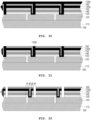
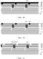
- FIG. 2 is a schematic view illustrating the perovskite solar cell module according to the first embodiment.
- the perovskite solar cell module 100 includes a substrate 110, a first electrode 120, a first charge transport layer 130, a photoactive layer 140, a second charge transport layer 150, a functional layer 150a, and a second electrode 160.
- the first electrode 120 is stacked on an upper surface of the substrate 110, and patterned through physical and chemical removal, such as dry etching, wet etching, laser, and mechanical processing, to be separated with first spaces a1 formed therein.
- the first charge transport layer 130, the photoactive layer 140, and the second charge transport layer 150 are sequentially stacked on upper surfaces of the separated first electrodes 120.
- the first charge transport layer 130, the photoactive layer 140, and the second charge transport layer 150 stacked on the separated first electrodes 120 are patterned through physical and chemical removal, such as dry etching, wet etching, laser, and mechanical processing, to be separated with second spaces a2 formed therein.
- the functional layer 150a is stacked on upper surfaces of the separated second charge transport layers 150 and in the second spaces a2 formed between the separated first charge transport layers 130, the separated photoactive layers 140, and the separated second charge transport layers 150.
- the second electrode 160 is stacked on an upper surface of the functional layer 150a.
- the second electrode 160 is patterned through physical and chemical removal, such as dry etching, wet etching, laser, and mechanical processing, to be separated with third spaces a3 formed therein.
- perovskite solar cell modules described in detail below that are modified from the first embodiment are configured in a manner similar to that described in FIG. 2 , a detailed description thereof will be omitted. However, when structural changes, modifications, and variations are made therein, a description thereof will be given.
- FIGS. 3 to 13 are views illustrating other examples of the perovskite solar cell module according to the first embodiment illustrated in FIG. 2 .
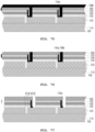
- FIG. 3 is a view illustrating a first example of the perovskite solar cell module according to the first embodiment.
- the first example of the perovskite solar cell module according to the first embodiment including a substrate 110, a first electrode 120, a first charge transport layer 130, a photoactive layer 140, a second charge transport layer 150, a functional layer 150a, and a second electrode 160 further includes a functional layer 150b.
- the functional layer 150b is formed on a surface of each of separated second electrodes 160, and is stacked on upper surfaces of the separated second electrodes 160 and in third spaces a3 formed between the separated second electrodes 160.
- FIG. 4 is a view illustrating a second example of the perovskite solar cell module according to the first embodiment.
- the second example of the perovskite solar cell module according to the first embodiment including a substrate 110, a first electrode 120, a first charge transport layer 130, a photoactive layer 140, a second charge transport layer 150, a functional layer 150a, and a second electrode 160 further includes a functional layer 150b.
- the functional layer 150b is formed on a surface of each of separated second electrodes 160, and is stacked in third spaces a3 formed between the separated second electrodes 160.
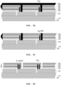
- FIG. 5 is a view illustrating a third example of the perovskite solar cell module according to the first embodiment.
- the third example of the perovskite solar cell module according to the first embodiment includes a substrate 110, a first electrode 120, a first charge transport layer 130, a photoactive layer 140, a second charge transport layer 150, a functional layer 150a, and a second electrode 160.
- the first charge transport layer 130, the photoactive layer 140, and the second charge transport layer 150 are stacked on separated first electrodes 120 and patterned through physical and chemical removal, such as dry etching, wet etching, laser, and mechanical processing, to be separated with second spaces a2 formed therein.
- the first charge transport layer 130, the photoactive layer 140, and the second charge transport layer 150 are patterned so that a first gap g1 exists between a first space a1 and a second space a2.
- Perovskite solar cell modules modified from the third example of the perovskite solar cell module according to the first embodiment described above with reference to FIG. 5 will be described with reference to FIGS. 6 and 7 .
- FIG. 6 is a view illustrating a fourth example of the perovskite solar cell module according to the first embodiment.
- the fourth example of the perovskite solar cell module according to the first embodiment including a substrate 110, a first electrode 120, a first charge transport layer 130, a photoactive layer 140, a second charge transport layer 150, a functional layer 150a, and a second electrode 160 further includes a functional layer 150b.
- the functional layer 150b is formed on a surface of each of separated second electrodes 160, and is stacked on upper surfaces of the separated second electrodes 160 and in third spaces a3 formed between the separated second electrodes 160.
- FIG. 7 is a view illustrating a fifth example of the perovskite solar cell module according to the first embodiment.
- the fifth example of the perovskite solar cell module according to the first embodiment including a substrate 110, a first electrode 120, a first charge transport layer 130, a photoactive layer 140, a second charge transport layer 150, a functional layer 150a, and a second electrode 160 further includes a functional layer 150b.
- the functional layer 150b is formed on a surface of each of separated second electrodes 160, and is stacked in third spaces a3 formed between the separated second electrodes 160.
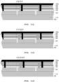
- FIG. 8 is a view illustrating a sixth example of the perovskite solar cell module according to the first embodiment.
- the sixth example of the perovskite solar cell module according to the first embodiment includes a substrate 110, a first electrode 120, a first charge transport layer 130, a photoactive layer 140, a second charge transport layer 150, a functional layer 150a, and a second electrode 160.
- the second electrode 160 is stacked on an upper surface of the functional layer 150a and patterned to be separated with third spaces a3 formed therein.
- the second electrode 160 is patterned so that a second gap g2 exists between a second space a2 and a third space a3.
- Perovskite solar cell modules modified from the sixth example of the perovskite solar cell module according to the first embodiment described above with reference to FIG. 8 will be described with reference to FIGS. 9 and 10 .
- FIG. 9 is a view illustrating a seventh example of the perovskite solar cell module according to the first embodiment.
- the seventh example of the perovskite solar cell module according to the first embodiment including a substrate 110, a first electrode 120, a first charge transport layer 130, a photoactive layer 140, a second charge transport layer 150, a functional layer 150a, and a second electrode 160 further includes a functional layer 150b.
- the functional layer 150b is formed on a surface of each of separated second electrodes 160, and is stacked on upper surfaces of the separated second electrodes 160 and in third spaces a3 formed between the separated second electrodes 160.
- FIG. 10 is a view illustrating an eighth example of the perovskite solar cell module according to the first embodiment.
- the eighth example of the perovskite solar cell module according to the first embodiment including a substrate 110, a first electrode 120, a first charge transport layer 130, a photoactive layer 140, a second charge transport layer 150, a functional layer 150a, and a second electrode 160 further includes a functional layer 150b.
- the functional layer 150b is formed on a surface of each of separated second electrodes 160, and is stacked in third spaces a3 formed between the separated second electrodes 160.
- FIG. 11 is a view illustrating a ninth example of the perovskite solar cell module according to the first embodiment.
- the ninth example of the perovskite solar cell module according to the first embodiment includes a substrate 110, a first electrode 120, a first charge transport layer 130, a photoactive layer 140, a second charge transport layer 150, a functional layer 150a, and a second electrode 160.
- the first charge transport layer 130, the photoactive layer 140, and the second charge transport layer 150 are stacked on separated first electrodes 120 and patterned through physical and chemical removal, such as dry etching, wet etching, laser, and mechanical processing, to be separated with second spaces a2 formed therein.
- the first charge transport layer 130, the photoactive layer 140, and the second charge transport layer 150 are patterned so that a first gap g1 exists between a first space a1 and a second space a2.
- the second electrode 160 is stacked on an upper surface of the functional layer 150a and patterned through physical and chemical removal, such as dry etching, wet etching, laser, and mechanical processing, to be separated with third spaces a3 formed therein.
- the second electrode 160 is patterned so that a second gap g2 exists between a second space a2 and a third space a3.
- Perovskite solar cell modules modified from the ninth example of the perovskite solar cell module according to the first embodiment described above with reference to FIG. 11 will be described with reference to FIGS. 12 and 13 .
- FIG. 12 is a view illustrating a tenth example of the perovskite solar cell module according to the first embodiment.
- the tenth example of the perovskite solar cell module according to the first embodiment including a substrate 110, a first electrode 120, a first charge transport layer 130, a photoactive layer 140, a second charge transport layer 150, a functional layer 150a, and a second electrode 160 further includes a functional layer 150b.
- the functional layer 150b is stacked on upper surfaces of separated second electrodes 160 and in third spaces a3 formed between the separated second electrodes 160.
- FIG. 13 is a view illustrating an eleventh example of the perovskite solar cell module according to the first embodiment.
- the eleventh example of the perovskite solar cell module according to the first embodiment including a substrate 110, a first electrode 120, a first charge transport layer 130, a photoactive layer 140, a second charge transport layer 150, a functional layer 150a, and a second electrode 160 further includes a functional layer 150b.
- the functional layer 150b is stacked in third spaces a3 formed between separated second electrodes 160.
- FIGS. 14 to 25 are views illustrating modified structures of the first to eleventh examples of the perovskite solar cell module according to the first embodiment described above.
- a functional layer 150a is patterned through physical and chemical removal, such as dry etching, wet etching, laser, and mechanical processing, so that each second electrode 160 is in contact with and electrically connected to an adjacent first electrode 120.
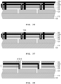
- FIG. 26 is a schematic view illustrating a perovskite solar cell module according to a second embodiment.
- the perovskite solar cell module 100 includes a substrate 110, a first electrode 120, a first charge transport layer 130, a photoactive layer 140, a second charge transport layer 150, a functional layer 150a, and a second electrode 160.
- the first electrode 120 is stacked on an upper surface of the substrate 110, and patterned through physical and chemical removal, such as dry etching, wet etching, laser, and mechanical processing, to be separated with first spaces a1 formed therein.
- the first charge transport layer 130, the photoactive layer 140, and the second charge transport layer 150 are sequentially stacked on upper surfaces of the separated first electrodes 120.
- the first charge transport layer 130, the photoactive layer 140, and the second charge transport layer 150 stacked on the separated first electrodes 120 are patterned through physical and chemical removal, such as dry etching, wet etching, laser, and mechanical processing, to be separated with second spaces a2 formed therein.
- the functional layer 150a is stacked on upper surfaces of the separated second charge transport layers 150 and in the second spaces a2.
- the second electrode 160 is stacked on an upper surface of the functional layer 150a.
- the separated first charge transport layers 130, the separated photoactive layers 140, the separated second charge transport layers 150, the functional layer 150a, and the second electrode 160 stacked on the separated first electrodes 120 are patterned through physical and chemical removal, such as dry etching, wet etching, laser, and mechanical processing, to be separated with third spaces a3 formed therein.
- perovskite solar cell modules described in detail below that are modified from the second embodiment are configured in a manner similar to that described in FIG. 26 , a detailed description thereof will be omitted. However, when structural changes, modifications, and variations are made therein, a description thereof will be given.
- FIGS. 27 to 49 are views illustrating other examples of the perovskite solar cell module according to the second embodiment illustrated in FIG. 26 .
- FIG. 27 is a view illustrating a first example of the perovskite solar cell module according to the second embodiment.
- the first example of the perovskite solar cell module according to the second embodiment including a substrate 110, a first electrode 120, a first charge transport layer 130, a photoactive layer 140, a second charge transport layer 150, a functional layer 150a, and a second electrode 160 further includes a functional layer 150b.
- the functional layer 150b is formed on a surface of each of separated second electrodes 160, and is stacked on upper surfaces of the separated second electrodes 160 and in third spaces a3 formed between separated first charge transport layers 130, separated photoactive layers 140, separated second charge transport layers 150, separated functional layers 150a, and the separated second electrodes 160.
- FIG. 28 is a view illustrating a second example of the perovskite solar cell module according to the second embodiment.
- the second example of the perovskite solar cell module according to the second embodiment including a substrate 110, a first electrode 120, a first charge transport layer 130, a photoactive layer 140, a second charge transport layer 150, a functional layer 150a, and a second electrodes 160 further includes a functional layer 150b.
- the functional layer 150b is formed on a surface of each of separated second electrodes 160, and is stacked in third spaces a3 formed between separated first charge transport layers 130, separated photoactive layers 140, separated second charge transport layers 150, separated functional layers 150a, and the separated second electrodes 160.
- FIG. 29 is a view illustrating a third example of the perovskite solar cell module according to the second embodiment.
- the third example of the perovskite solar cell module according to the second embodiment includes a substrate 110, a first electrode 120, a first charge transport layer 130, a photoactive layer 140, a second charge transport layer 150, a functional layer 150a, and a second electrode 160.
- the first charge transport layer 130, the photoactive layer 140, and the second charge transport layer 150 are stacked on separated first electrodes 120 and patterned through physical and chemical removal, such as dry etching, wet etching, laser, and mechanical processing, to be separated with second spaces a2 formed therein.
- the first charge transport layer 130, the photoactive layer 140, and the second charge transport layer 150 are patterned so that a first gap g1 exists between a first space a1 and a second space a2.
- Perovskite solar cell modules modified from the third example of the perovskite solar cell module according to the second embodiment described above with reference to FIG. 29 will be described with reference to FIGS. 30 and 31 .
- FIG. 30 is a view illustrating a fourth example of the perovskite solar cell module according to the second embodiment.
- the fourth example of the perovskite solar cell module according to the second embodiment including a substrate 110, a first electrode 120, a first charge transport layer 130, a photoactive layer 140, a second charge transport layer 150, a functional layer 150a, and a second electrode 160 further includes a functional layer 150b.
- the functional layer 150b is formed on a surface of each of separated second electrodes 160, and is stacked on upper surfaces of the separated second electrodes 160 and in third spaces a3 formed between separated first charge transport layers 130, separated photoactive layers 140, separated second charge transport layers 150, separated functional layers 150a, and the separated second electrodes 160.
- FIG. 31 is a view illustrating a fifth example of the perovskite solar cell module according to the second embodiment.
- the fifth example of the perovskite solar cell module according to the second embodiment including a substrate 110, a first electrode 120, a first charge transport layer 130, a photoactive layer 140, a second charge transport layer 150, a functional layer 150a, and a second electrode 160 further includes a functional layer 150b.
- the functional layer 150b is stacked in third spaces a3 formed between separated first charge transport layers 130, separated photoactive layers 140, separated second charge transport layers 150, separated functional layers 150a, and separated second electrodes 160.
- FIG. 32 is a view illustrating a sixth example of the perovskite solar cell module according to the second embodiment.
- the sixth example of the perovskite solar cell module according to the second embodiment includes a substrate 110, a first electrode 120, a first charge transport layer 130, a photoactive layer 140, a second charge transport layer 150, a functional layer 150a, and a second electrode 160.
- Separated first charge transport layers 130, separated photoactive layers 140, separated second charge transport layers 150, the functional layer 150a, and the second electrode 160 stacked on separated first electrodes 120 are patterned through physical and chemical removal, such as dry etching, wet etching, laser, and mechanical processing, to be separated with second spaces a2 formed therein.
- the separated first charge transport layers 130, the separated photoactive layers 140, the separated second charge transport layers 150, the functional layer 150a, and the second electrode 160 are patterned so that a second gap g2 exists between a second space a2 and a third space a3.
- Perovskite solar cell modules modified from the sixth example of the perovskite solar cell module according to the second embodiment described above with reference to FIG. 32 will be described with reference to FIGS. 33 and 34 .
- FIG. 33 is a view illustrating a seventh example of the perovskite solar cell module according to the second embodiment.
- the seventh example of the perovskite solar cell module according to the second embodiment including a substrate 110, a first electrode 120, a first charge transport layer 130, a photoactive layer 140, a second charge transport layer 150, a functional layer 150a, and a second electrode 160 further includes a functional layer 150b.
- the functional layer 150b is formed on a surface of each of separated second electrodes 160, and is stacked on upper surfaces of the separated second electrodes 160 and in third spaces a3 formed between separated first charge transport layers 130, separated photoactive layers 140, separated second charge transport layers 150, separated functional layers 150a, and the separated second electrodes 160.
- FIG. 34 is a view illustrating an eighth example of the perovskite solar cell module according to the second embodiment.
- the eighth example of the perovskite solar cell module according to the second embodiment including a substrate 110, a first electrode 120, a first charge transport layer 130, a photoactive layer 140, a second charge transport layer 150, a functional layer 150a, and a second electrode 160 further includes a functional layer 150b.
- the functional layer 150b is stacked in third spaces a3 formed between separated first charge transport layers 130, separated photoactive layers 140, separated second charge transport layers 150, separated functional layers 150a, and separated second electrodes 160.
- FIG. 35 is a view illustrating a ninth example of the perovskite solar cell module according to the second embodiment.
- the ninth example of the perovskite solar cell module according to the second embodiment includes a substrate 110, a first electrode 120, a first charge transport layer 130, a photoactive layer 140, a second charge transport layer 150, a functional layer 150a, and a second electrode 160.
- the first charge transport layer 130, the photoactive layer 140, and the second charge transport layer 150 are stacked on separated first electrodes 120 and patterned through physical and chemical removal, such as dry etching, wet etching, laser, and mechanical processing, to be separated with second spaces a2 formed therein.
- the first charge transport layer 130, the photoactive layer 140, and the second charge transport layer 150 are patterned so that a first gap g1 exists between a first space a1 and a second space a2.
- the separated first charge transport layers 130, the separated photoactive layers 140, the separated second charge transport layers 150, the functional layer 150a, and the second electrode 160 stacked on the separated first electrode 120 are patterned through physical and chemical removal, such as dry etching, wet etching, laser, and mechanical processing, to be separated with third spaces a3 formed therein.
- the separated first charge transport layers 130, the separated photoactive layers 140, the separated second charge transport layers 150, the functional layer 150a, and the second electrode 160 are patterned so that a second gap g2 exists between a second space a2 and a third space a3.
- Perovskite solar cell modules modified from the ninth example of the perovskite solar cell module according to the second embodiment described above with reference to FIG. 35 will be described with reference to FIGS. 36 and 37 .
- FIG. 36 is a view illustrating a tenth example of the perovskite solar cell module according to the second embodiment.
- the tenth example of the perovskite solar cell module according to the second embodiment including a substrate 110, a first electrode 120, a first charge transport layer 130, a photoactive layer 140, a second charge transport layer 150, a functional layer 150a, and a second electrode 160 further includes a functional layer 150b.
- the functional layer 150b is formed on a surface of each of separated second electrodes 160, and is stacked on upper surfaces of the separated second electrodes 160 and in third spaces a3 formed between separated first charge transport layers 130, separated photoactive layers 140, separated second charge transport layers 150, separated functional layers 150a, and the separated second electrodes 160.
- FIG. 37 is a view illustrating an eleventh example of the perovskite solar cell module according to the second embodiment.
- the eleventh example of the perovskite solar cell module according to the second embodiment including a substrate 110, a first electrode 120, a first charge transport layer 130, a photoactive layer 140, a second charge transport layer 150, a functional layer 150a, and a second electrode 160 further includes a functional layer 150b.
- the functional layer 150b is formed on a surface of each of separated second electrodes 160, and is stacked in third spaces a3 formed between separated first charge transport layers 130, separated photoactive layers 140, separated second charge transport layers 150, separated functional layers 150a, and the separated second electrodes 160.
- FIGS. 38 to 39 are views illustrating modified structures of the first to eleventh examples of the perovskite solar cell module according to the second embodiment described above.
- a functional layer 150a is patterned through physical and chemical removal, such as dry etching, wet etching, laser, and mechanical processing, so that each second electrode 160 is in contact with and electrically connected to an adjacent first electrode 120.
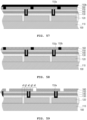
- FIG. 50 is a schematic view illustrating a perovskite solar cell module according to a third embodiment.
- the perovskite solar cell module 100 includes a substrate 110, a first electrode 120, a first charge transport layer 130, a photoactive layer 140, a second charge transport layer 150, a functional layer 150a, and a second electrode 160.
- the first electrode 120 is formed on an upper surface of the substrate 110, and patterned through physical and chemical removal, such as dry etching, wet etching, laser, and mechanical processing, to be separated with first spaces a1 formed therein.
- the first charge transport layer 130, the photoactive layer 140, and the second charge transport layer 150 are sequentially stacked on upper surfaces of the separated first electrodes 120.
- the first charge transport layer 130, the photoactive layer 140, and the second charge transport layer 150 stacked on the separated first electrodes 120 are patterned through physical and chemical removal, such as dry etching, wet etching, laser, and mechanical processing, to be separated with second spaces a2 formed therein.
- the functional layer 150a is stacked in the second spaces a2 formed between the separated first charge transport layers 130, the separated photoactive layers 140, and the separated second charge transport layers 150.
- the second electrode 160 is stacked on upper surfaces of the separated second charge transport layers 150 and upper surfaces of separated functional layers 150a.
- the second electrode 160 is patterned through physical and chemical removal, such as dry etching, wet etching, laser, and mechanical processing, to be separated with third spaces a3 formed therein.
- perovskite solar cell modules described in detail below are configured in the same manner as those according to the third embodiment described above with reference to FIG. 50 and including the substrate 110, the first electrode 120, the first charge transport layer 130, the photoactive layer 140, the second charge transport layers 150, the functional layer 150a, and the second electrode 160, a detailed description thereof will be omitted. However, when structural changes, modifications, and variations are made therein, a description thereof will be given.
- FIGS. 51 to 52 are views illustrating other examples of the perovskite solar cell module according to the third embodiment illustrated in FIG. 50 .
- FIG. 51 is a view illustrating a first example of the perovskite solar cell module according to the third embodiment.
- the first example of the perovskite solar cell module according to the third embodiment including a substrate 110, a first electrode 120, a first charge transport layer 130, a photoactive layer 140, a second charge transport layer 150, a functional layer 150a, and a second electrode 160 further includes a functional layer 150b.
- the functional layer 150b is formed on a surface of each of separated second electrodes 160, and is stacked on upper surfaces of the separated second electrodes 160 and in third spaces a3 formed between the separated second electrodes 160.
- FIG. 52 is a view illustrating a second example of the perovskite solar cell module according to the third embodiment.
- the second example of the perovskite solar cell module according to the third embodiment including a substrate 110, a first electrode 120, a first charge transport layer 130, a photoactive layer 140, a second charge transport layer 150, a functional layer 150a, and a second electrode 160 further includes a functional layer 150b formed on a surface of the second electrode 160.
- the functional layer 150b is formed on a surface of each of separated second electrodes 160, and is stacked in third spaces a3 formed between the separated second electrodes 160.
- FIG. 53 is a view illustrating a third example of the perovskite solar cell module according to the third embodiment.
- the third example of the perovskite solar cell module according to the third embodiment includes a substrate 110, a first electrode 120, a first charge transport layer 130, a photoactive layer 140, a second charge transport layer 150, a functional layer 150a, and a second electrode 160.
- the first charge transport layer 130, the photoactive layer 140, and the second charge transport layer 150 are stacked on separated first electrodes 120 and patterned through physical and chemical removal, such as dry etching, wet etching, laser, and mechanical processing, to be separated with second spaces a2 formed therein.
- the first charge transport layer 130, the photoactive layer 140, and the second charge transport layer 150 are patterned so that a first gap g1 exists between a first space a1 and a second space a2.
- Perovskite solar cell modules modified from the third example of the perovskite solar cell module according to the third embodiment described above with reference to FIG. 53 will be described with reference to FIGS. 54 and 55 .
- FIG. 54 is a view illustrating a fourth example of the perovskite solar cell module according to the third embodiment.
- the fourth example of the perovskite solar cell module according to the third embodiment including a substrate 110, a first electrode 120, a first charge transport layer 130, a photoactive layer 140, a second charge transport layer 150, a functional layer 150a, and a second electrode 160 further includes a functional layer 150b.
- the functional layer 150b is formed on a surface of each of separated second electrodes 160, and is stacked on upper surfaces of the separated second electrodes 160 and in third spaces a3 formed between the separated second electrodes 160.
- FIG. 55 is a view illustrating a fifth example of the perovskite solar cell module according to the third embodiment.
- the fifth example of the perovskite solar cell module according to the third embodiment including a substrate 110, a first electrode 120, a first charge transport layer 130, a photoactive layer 140, a second charge transport layer 150, a functional layer 150a, and a second electrode 160 further includes a functional layer 150b.
- the functional layer 150b is formed on a surface of each of separated second electrodes 160, and is stacked in third spaces a3 formed between the separated second electrodes 160.
- FIG. 56 is a view illustrating a sixth example of the perovskite solar cell module according to the third embodiment.
- the sixth example of the perovskite solar cell module according to the third embodiment includes a substrate 110, a first electrode 120, a first charge transport layer 130, a photoactive layer 140, a second charge transport layer 150, a functional layer 150a, and a second electrode 160.
- the second electrode 160 is stacked on upper surfaces of separated second charge transport layers 150 and upper surfaces of separated functional layers 150a, and patterned through physical and chemical removal, such as dry etching, wet etching, laser, and mechanical processing, to be separated with third spaces a3 formed therein.
- the second electrode 160 is patterned so that a second gap g2 exists between a second space a2 and a third space a3.
- Perovskite solar cell modules modified from the sixth example of the perovskite solar cell module according to the third embodiment described above with reference to FIG. 56 will be described with reference to FIGS. 57 and 58 .
- FIG. 57 is a view illustrating a seventh example of the perovskite solar cell module according to the third embodiment.
- the seventh example of the perovskite solar cell module according to the third embodiment including a substrate 110, a first electrode 120, a first charge transport layer 130, a photoactive layer 140, a second charge transport layer 150, a functional layer 150a, and a second electrode 160 further includes a functional layer 150b.
- the functional layer 150b is formed on a surface of each of separated second electrodes 160, and is stacked on upper surfaces of the separated second electrodes 160 and in third spaces a3 formed between the separated second electrodes 160.
- FIG. 58 is a view illustrating an eighth example of the perovskite solar cell module according to the third embodiment.
- the eighth example of the perovskite solar cell module according to the third embodiment including a substrate 110, a first electrode 120, a first charge transport layer 130, a photoactive layer 140, a second charge transport layer 150, a functional layer 150a, and a second electrode 160 further includes a functional layer 150b.
- the functional layer 150b is formed on a surface of each of separated second electrodes 160, and is stacked in third spaces a3 formed between the separated second electrodes 160.
- FIG. 59 is a view illustrating a ninth example of the perovskite solar cell module according to the third embodiment.
- the ninth example of the perovskite solar cell module according to the third embodiment includes a substrate 110, a first electrode 120, a first charge transport layer 130, a photoactive layer 140, a second charge transport layer 150, a functional layer 150a, and a second electrode 160.
- the first charge transport layer 130, the photoactive layer 140, and the second charge transport layer 150 are stacked on separated first electrodes 120 and patterned through physical and chemical removal, such as dry etching, wet etching, laser, and mechanical processing, to be separated with second spaces a2 formed therein.
- the first charge transport layer 130, the photoactive layer 140, and the second charge transport layer 150 are patterned so that a first gap g1 exists between a first space a1 and a second space a2.
- the second electrode 160 is stacked on upper surfaces of the separated second charge transport layers 150 and upper surfaces of separated functional layers 150a, and patterned through physical and chemical removal, such as dry etching, wet etching, laser, and mechanical processing, to be separated with third spaces a3 formed therein.
- the second electrode 160 is patterned so that a second gap g2 exists between a second space a2 and a third space a3.
- Perovskite solar cell modules modified from the ninth example of the perovskite solar cell module according to the third embodiment described above with reference to FIG. 59 will be described with reference to FIGS. 60 and 61 .
- FIG. 60 is a view illustrating a tenth example of the perovskite solar cell module according to the third embodiment.
- the tenth example of the perovskite solar cell module according to the third embodiment including a substrate 110, a first electrode 120, a first charge transport layer 130, a photoactive layer 140, a second charge transport layer 150, a functional layer 150a, and a second electrode 160 further includes a functional layer 150b.
- the functional layer 150b is stacked on upper surfaces of separated second electrodes 160 and in third spaces a3 formed between the separated second electrodes 160.
- FIG. 61 is a view illustrating an eleventh example of the perovskite solar cell module according to the third embodiment.
- the eleventh example of the perovskite solar cell module according to the third embodiment including a substrate 110, a first electrode 120, a first charge transport layer 130, a photoactive layer 140, a second charge transport layer 150, a functional layer 150a, and a second electrode 160 further includes a functional layer 150b.
- the functional layer 150b is stacked in third spaces a3 formed between separated second electrodes 160.
- FIGS. 62 to 73 are views illustrating modified structures of the first to eleventh examples of the perovskite solar cell module according to the third embodiment described above.
- a functional layer 150a is patterned through physical and chemical removal, such as dry etching, wet etching, laser, and mechanical processing, so that each second electrode 160 is in contact with and electrically connected to an adjacent first electrode 120.
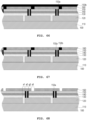
- FIG. 74 is a schematic view illustrating a perovskite solar cell module according to a fourth embodiment.
- the perovskite solar cell module 100 includes a substrate 110, a first electrode 120, a first charge transport layer 130, a photoactive layer 140, a second charge transport layer 150, a functional layer 150a, and a second electrode 160.
- the first electrode 120 is stacked on an upper surface of the substrate 110, and patterned through physical and chemical removal, such as dry etching, wet etching, laser, and mechanical processing, to be separated with first spaces a1 formed therein.
- the first charge transport layer 130 is stacked on upper surfaces of the separated first electrodes 120 and in the first spaces a1 formed between the separated first electrodes 120.
- the photoactive layer 140 and the second charge transport layer 150 are sequentially stacked on an upper surface of the first charge transport layer 130.
- the first charge transport layer 130, the photoactive layer 140, and the second charge transport layer 150 stacked on the separated first electrodes 120 are patterned through physical and chemical removal, such as dry etching, wet etching, laser, and mechanical processing, to be separated with second spaces a2 formed therein.
- the functional layer 150a is stacked in the second spaces a2 formed between the separated first charge transport layers 130, the separated photoactive layers 140, and the separated second charge transport layers 150.
- the second electrode 160 is stacked on upper surfaces of the separated second charge transport layers 150 and upper surfaces of separated functional layers 150a.
- the separated first charge transport layers 130, the separated photoactive layers 140, the separated second charge transport layers 150, and the second electrode 160 stacked on the separated first electrodes 120 are patterned through physical and chemical removal, such as dry etching, wet etching, laser, and mechanical processing, to be separated with third spaces a3 formed therein.
- perovskite solar cell modules described in detail below are configured in the same manner as those according to the fourth embodiment described above with reference to FIG. 74 and including the substrate 110, the first electrode 120, the first charge transport layer 130, the photoactive layer 140, the second charge transport layers 150, the functional layer 150a, and the second electrode 160, a detailed description thereof will be omitted. However, when structural changes, modifications, and variations are made therein, a description thereof will be given.
- FIGS. 75 to 76 are views illustrating other examples of the perovskite solar cell module according to the fourth embodiment illustrated in FIG. 74 .
- FIG. 75 is a view illustrating a first example of the perovskite solar cell module according to the fourth embodiment.
- the first example of the perovskite solar cell module according to the fourth embodiment including a substrate 110, a first electrode 120, a first charge transport layer 130, a photoactive layer 140, a second charge transport layer 150, a functional layer 150a, and a second electrode 160 further includes a functional layer 150b.
- the functional layer 150b is formed on a surface of each of separated second electrodes 160, and is stacked on upper surfaces of the separated second electrodes 160 and in third spaces a3 formed between separated first charge transport layers 130, separated photoactive layers 140, separated second charge transport layers 150, and the separated second electrodes 160.
- FIG. 76 is a view illustrating a second example of the perovskite solar cell module according to the fourth embodiment.
- the second example of the perovskite solar cell module according to the fourth embodiment including a substrate 110, a first electrode 120, a first charge transport layer 130, a photoactive layer 140, a second charge transport layer 150, a functional layer 150a, and a second electrode 160 further includes a functional layer 150b.
- the functional layer 150b is stacked in third spaces a3 formed between separated first charge transport layers 130, separated photoactive layers 140, separated second charge transport layers 150, and separated second electrodes 160.
- FIG. 77 is a view illustrating a third example of the perovskite solar cell module according to the fourth embodiment.
- the third example of the perovskite solar cell module according to the fourth embodiment includes a substrate 110, a first electrode 120, a first charge transport layer 130, a photoactive layer 140, a second charge transport layer 150, a functional layer 150a, and a second electrode 160.
- the first charge transport layer 130, the photoactive layer 140, and the second charge transport layer 150 are stacked on separated first electrodes 120 and patterned through physical and chemical removal, such as dry etching, wet etching, laser, and mechanical processing, to be separated with second spaces a2 formed therein.
- the first charge transport layer 130, the photoactive layer 140, and the second charge transport layer 150 are patterned so that a first gap g1 exists between a first space a1 and a second space a2.
- Perovskite solar cell modules modified from the third example of the perovskite solar cell module according to the fourth embodiment described above with reference to FIG. 77 will be described with reference to FIGS. 78 and 79 .
- FIG. 78 is a view illustrating a fourth example of the perovskite solar cell module according to the fourth embodiment.
- the fourth example of the perovskite solar cell module according to the fourth embodiment including a substrate 110, a first electrode 120, a first charge transport layer 130, a photoactive layer 140, a second charge transport layer 150, a functional layer 150a, and a second electrode 160 further includes a functional layer 150b.
- the functional layer 150b is formed on a surface of each of separated second electrodes 160, and is stacked on upper surfaces of the separated second electrodes 160 and in third spaces a3 formed between separated first charge transport layers 130, separated photoactive layers 140, separated second charge transport layers 150, and the separated second electrodes 160.
- FIG. 79 is a view illustrating a fifth example of the perovskite solar cell module according to the fourth embodiment.
- the fifth example of the perovskite solar cell module according to the fourth embodiment including a substrate 110, a first electrode 120, a first charge transport layer 130, a photoactive layer 140, a second charge transport layer 150, a functional layer 150a, and a second electrode 160 further includes a functional layer 150b.
- the functional layer 150b is stacked in third spaces a3 formed between separated first charge transport layers 130, separated photoactive layers 140, separated second charge transport layers 150, and separated second electrodes 160.
- FIG. 80 is a view illustrating a sixth example of the perovskite solar cell module according to the fourth embodiment.
- the sixth example of the perovskite solar cell module according to the fourth embodiment includes a substrate 110, a first electrode 120, a first charge transport layer 130, a photoactive layer 140, a second charge transport layer 150, a functional layer 150a, and a second electrode 160.
- Separated first charge transport layers 130, separated photoactive layers 140, separated second charge transport layers 150, and the second electrode 160 stacked on separated first electrodes 120 are patterned through physical and chemical removal, such as dry etching, wet etching, laser, and mechanical processing, to be separated with third spaces formed therein.
- the separated first charge transport layers 130, the separated photoactive layers 140, the separated second charge transport layers 150, and the second electrode 160 are patterned so that a second gap g2 exists between a second space a2 and a third space a3.
- Perovskite solar cell modules modified from the sixth example of the perovskite solar cell module according to the fourth embodiment described above with reference to FIG. 80 will be described with reference to FIGS. 81 and 82 .
- FIG. 81 is a view illustrating a seventh example of the perovskite solar cell module according to the fourth embodiment.
- the seventh example of the perovskite solar cell module according to the fourth embodiment including a substrate 110, a first electrode 120, a first charge transport layer 130, a photoactive layer 140, a second charge transport layer 150, a functional layer 150a, and a second electrode 160 further includes a functional layer 150b.
- the functional layer 150b is formed on a surface of each of separated second electrodes 160, and is stacked on upper surfaces of the separated second electrodes 160 and in third spaces a3 formed between separated first charge transport layers 130, separated photoactive layers 140, separated second charge transport layers 150, and the separated second electrodes 160.
- FIG. 82 is a view illustrating an eighth example of the perovskite solar cell module according to the fourth embodiment.
- the eighth example of the perovskite solar cell module according to the fourth embodiment including a substrate 110, a first electrode 120, a first charge transport layer 130, a photoactive layer 140, a second charge transport layer 150, a functional layer 150a, and a second electrode 160 further includes a functional layer 150b.
- the functional layer 150b is stacked in third spaces a3 formed between separated first charge transport layers 130, separated photoactive layers 140, separated second charge transport layers 150, and separated second electrodes 160.
- FIG. 83 is a view illustrating a ninth example of the perovskite solar cell module according to the fourth embodiment.
- the ninth example of the perovskite solar cell module according to the fourth embodiment includes a substrate 110, a first electrode 120, a first charge transport layer 130, a photoactive layer 140, a second charge transport layer 150, a functional layer 150a, and a second electrode 160.
- the first charge transport layer 130, the photoactive layer 140, and the second charge transport layer 150 are stacked on separated first electrodes 120 and patterned through physical and chemical removal, such as dry etching, wet etching, laser, and mechanical processing, to be separated with second spaces a2 formed therein.
- the first charge transport layer 130, the photoactive layer 140, and the second charge transport layer 150 are patterned so that a first gap g1 exists between a first space a1 and a second space a2.
- the separated first charge transport layers 130, the separated photoactive layers 140, the separated second charge transport layers 150, and the second electrode 160 stacked on the separated first electrodes 120 are patterned through physical and chemical removal, such as dry etching, wet etching, laser, and mechanical processing, to be separated with third spaces a3 formed therein.
- the separated first charge transport layers 130, the separated photoactive layers 140, the separated second charge transport layers 150, and the second electrode 160 are patterned so that a second gap g2 exists between a second space a2 and a third space a3.
- Perovskite solar cell modules modified from the ninth example of the perovskite solar cell module according to the fourth embodiment described above with reference to FIG. 83 will be described with reference to FIGS. 84 and 85 .
- FIG. 84 is a view illustrating a tenth example of the perovskite solar cell module according to the fourth embodiment.
- the tenth example of the perovskite solar cell module according to the fourth embodiment including a substrate 110, a first electrode 120, a first charge transport layer 130, a photoactive layer 140, a second charge transport layer 150, a functional layer 150a, and a second electrode 160 further includes a functional layer 150b.
- the functional layer 150b is formed on a surface of each of separated second electrodes 160, and is stacked on upper surfaces of the separated second electrodes 160 and in third spaces a3 formed between separated first charge transport layers 130, separated photoactive layers 140, separated second charge transport layers 150, and the separated second electrodes 160.
- FIG. 85 is a view illustrating an eleventh example of the perovskite solar cell module according to the fourth embodiment.
- the eleventh example of the perovskite solar cell module according to the fourth embodiment including a substrate 110, a first electrode 120, a first charge transport layer 130, a photoactive layer 140, a second charge transport layer 150, a functional layer 150a, and a second electrode 160 further includes a functional layer 150b.
- the functional layer 150b is stacked in third spaces a3 formed between separated first charge transport layers 130, separated photoactive layers 140, separated second charge transport layers 150, and separated second electrodes 160.
- FIGS. 86 to 97 are views illustrating modified structures of the first to eleventh examples of the perovskite solar cell module according to the fourth embodiment described above.
- a functional layer 150a is patterned through physical and chemical removal, such as dry etching, wet etching, laser, and mechanical processing, so that each second electrode 160 is in contact with and electrically connected to an adjacent first electrode 120.
- FIG. 98 is a schematic view illustrating a perovskite solar cell module according to a fifth embodiment.
- the perovskite solar cell module 100 includes a substrate 110, a first electrode 120, a first charge transport layer 130, a photoactive layer 140, a second charge transport layer 150, a functional layer 150a, and a second electrode 160.
- the first electrode 120 is stacked on an upper surface of the substrate 110, and patterned through physical and chemical removal, such as dry etching, wet etching, laser, and mechanical processing, to be separated with first spaces a1 formed therein.
- the first charge transport layer 130 is stacked on upper surfaces of the separated first electrodes 120 and in the first spaces a1 formed between the separated first electrodes 120.
- the photoactive layer 140 and the second charge transport layer 150 are sequentially stacked on an upper surface of the first charge transport layer 130.
- the first charge transport layer 130, the photoactive layer 140, and the second charge transport layer 150 stacked on the separated first electrodes 120 are patterned through physical and chemical removal, such as dry etching, wet etching, laser, and mechanical processing, to be separated with second spaces a2 formed therein.
- the second electrode 160 is stacked on upper surfaces of the separated second charge transport layers 150 and in the second spaces a2 formed between the separated first charge transport layers 130, the separated photoactive layers 140, and the separated second charge transport layers 150.
- the second electrode 160 is patterned through physical and chemical removal, such as dry etching, wet etching, laser, and mechanical processing, to be separated with third spaces a3 formed therein.
- the functional layer 150a is stacked in the third spaces a3 formed between the separated second electrodes 160.
- perovskite solar cell modules described in detail below are configured in the same manner as those according to the fifth embodiment described above with reference to FIG. 98 and including the substrate 110, the first electrode 120, the first charge transport layer 130, the photoactive layer 140, the second charge transport layers 150, the second electrode 160, and the functional layer 150a, a detailed description thereof will be omitted. However, when structural changes, modifications, and variations are made therein, a description thereof will be given.
- FIGS. 99 to 105 are views illustrating other examples of the perovskite solar cell module according to the fifth embodiment.
- FIG. 99 is a view illustrating a first example of the perovskite solar cell module according to the fifth embodiment.
- the first example of the perovskite solar cell module according to the fifth embodiment includes a substrate 110, a first electrode 120, a first charge transport layer 130, a photoactive layer 140, a second charge transport layer 150, a functional layer 150a, and a second electrode 160.
- the first charge transport layer 130, the photoactive layer 140, and the second charge transport layer 150 are stacked on separated first electrodes 120 and patterned through physical and chemical removal, such as dry etching, wet etching, laser, and mechanical processing, to be separated with second spaces a2 formed therein.
- the first charge transport layer 130, the photoactive layer 140, and the second charge transport layer 150 are patterned so that a first gap g1 exists between a first space a1 and a second space a2.
- the second electrode 160 is stacked on upper surfaces of the separated second charge transport layers 150 and in the second spaces a2 formed between the separated first charge transport layers 130, the separated photoactive layers 140, and the separated second charge transport layers 150. After that, the second electrode 160 is patterned through physical and chemical removal, such as dry etching, wet etching, laser, and mechanical processing, to be separated with third spaces a3 formed therein.
- the functional layer 150a is stacked in the third spaces a3 formed between the separated second electrodes 160.
- FIG. 100 is a view illustrating a second example of the perovskite solar cell module according to the fifth embodiment.
- the second example of the perovskite solar cell module according to the fifth embodiment includes a substrate 110, a first electrode 120, a first charge transport layer 130, a photoactive layer 140, a second charge transport layer 150, a functional layer 150a, and a second electrode 160.
- the first charge transport layer 130, the photoactive layer 140, and the second charge transport layer 150 are stacked on separated first electrodes 120 and patterned through physical and chemical removal, such as dry etching, wet etching, laser, and mechanical processing, to be separated with second spaces a2 formed therein.
- the second electrode 160 is stacked on upper surfaces of the separated second charge transport layers 150 and in the second spaces a2 formed on the separated first electrodes 120.
- the second electrode 160 is patterned through physical and chemical removal, such as dry etching, wet etching, laser, and mechanical processing, to be separated with third spaces a3 formed therein.
- the second electrode 160 is patterned so that a second gap g2 exists between a second space a2 and a third space a3.
- the functional layer 150a is stacked in the third spaces a3 formed between the separated second electrodes 160.
- FIG. 101 is a view illustrating a third example of the perovskite solar cell module according to the fifth embodiment.
- the third example of the perovskite solar cell module according to the fifth embodiment includes a substrate 110, a first electrode 120, a first charge transport layer 130, a photoactive layer 140, a second charge transport layer 150, a functional layer 150a, and a second electrode 160.
- the first charge transport layer 130, the photoactive layer 140, and the second charge transport layer 150 are stacked on separated first electrodes 120 and patterned through physical and chemical removal, such as dry etching, wet etching, laser, and mechanical processing, to be separated with second spaces a2 formed therein.
- the first charge transport layer 130, the photoactive layer 140, and the second charge transport layer 150 are patterned so that a first gap g1 exists between a first space a1 and a second space a2.
- the second electrode 160 is stacked on upper surfaces of the separated second charge transport layers 150 and in the second spaces a2 formed on the separated first electrodes 120. After that, the second electrode 160 is patterned through physical and chemical removal, such as dry etching, wet etching, laser, and mechanical processing, to be separated with third spaces a3 formed therein. Here, the second electrode 160 is patterned so that a second gap g2 exists between a second space a2 and a third space a3.
- the functional layer 150a is stacked in the third spaces a3 formed between the second electrodes 160.
- FIG. 102 is a view illustrating a fourth example of the perovskite solar cell module according to the fifth embodiment.
- the fourth example of the perovskite solar cell module according to the fifth embodiment including a substrate 110, a first electrode 120, a first charge transport layer 130, a photoactive layer 140, a second charge transport layer 150, and a second electrode 160 further includes a functional layer 150a.
- the functional layer 150a is formed on a surface of each of separated second electrodes 160, and is stacked on upper surfaces of the separated second electrodes 160 and in third spaces a3 formed between the separated second electrodes 160.
- FIG. 103 is a view illustrating a fifth example of the perovskite solar cell module according to the fifth embodiment.
- the fifth example of the perovskite solar cell module according to the fifth embodiment includes a substrate 110, a first electrode 120, a first charge transport layer 130, a photoactive layer 140, a second charge transport layer 150, a second electrode 160, and a functional layer 150a.
- the first charge transport layer 130, the photoactive layer 140, and the second charge transport layer 150 are stacked on separated first electrodes 120 and patterned through physical and chemical removal, such as dry etching, wet etching, laser, and mechanical processing, to be separated with second spaces a2 formed therein.
- the first charge transport layer 130, the photoactive layer 140, and the second charge transport layer 150 are patterned so that a first gap g1 exists between a first space a1 and a second space a2.
- the second electrode 160 is stacked on upper surfaces of the separated second charge transport layers 150 and in the second spaces a2 formed between the separated first charge transport layers 130, the separated photoactive layers 140, and the separated second charge transport layers 150. After that, the second electrode 160 is patterned through physical and chemical removal, such as dry etching, wet etching, laser, and mechanical processing, to be separated with third spaces a3 formed therein.
- the functional layer 150a is stacked on upper surfaces of the separated second electrodes 160 and in the third spaces a3 formed between the separated second electrodes 160.
- FIG. 104 is a view illustrating a sixth example of the perovskite solar cell module according to the fifth embodiment.
- the sixth example of the perovskite solar cell module according to the fifth embodiment includes a substrate 110, a first electrode 120, a first charge transport layer 130, a photoactive layer 140, a second charge transport layer 150, a second electrode 160, and a functional layer 150a.
- the first charge transport layer 130, the photoactive layer 140, and the second charge transport layer 150 are stacked on separated first electrodes 120 and patterned through physical and chemical removal, such as dry etching, wet etching, laser, and mechanical processing, to be separated with second spaces a2 formed therein.
- the second electrode 160 is stacked on upper surfaces of the separated second charge transport layers 150 and in the second spaces a2 formed on the separated first electrodes 120. After that, the second electrode 160 is patterned through physical and chemical removal, such as dry etching, wet etching, laser, and mechanical processing, to be separated with third spaces a3 formed therein. Here, the second electrode 160 is patterned so that a second gap g2 exists between a second space a2 and a third space a3.
- the functional layer 150a is stacked on upper surfaces of the separated second electrodes 160 and in the third spaces a3 formed between the separated second electrodes 160.
- FIG. 105 is a view illustrating a seventh example of the perovskite solar cell module according to the fifth embodiment.
- the seventh example of the perovskite solar cell module according to the fifth embodiment includes a substrate 110, a first electrode 120, a first charge transport layer 130, a photoactive layer 140, a second charge transport layer 150, a second electrode 160, and a functional layer 150a.
- the first charge transport layer 130, the photoactive layer 140, and the second charge transport layer 150 are stacked on separated first electrodes 120 and patterned through physical and chemical removal, such as dry etching, wet etching, laser, and mechanical processing, to be separated with second spaces a2 formed therein.
- the first charge transport layer 130, the photoactive layer 140, and the second charge transport layer 150 are patterned so that a first gap g1 exists between a first space a1 and a second space a2.
- the second electrode 160 is stacked on upper surfaces of the separated second charge transport layers 150 and in the second spaces a2 formed on the separated first electrodes 120. After that, the second electrode 160 is patterned through physical and chemical removal, such as dry etching, wet etching, laser, and mechanical processing, to be separated with third spaces a3 formed therein. Here, the second electrode 160 is patterned so that a second gap g2 exists between a second space a2 and a third space a3.
- the functional layer 150a is stacked on upper surfaces of the separated second electrodes 160 and in the third spaces a3 formed between the separated second electrodes 160.
- FIG. 106 is a schematic view illustrating a perovskite solar cell module according to a sixth embodiment.
- the perovskite solar cell module 100 includes a substrate 110, a first electrode 120, a first charge transport layer 130, a photoactive layer 140, a second charge transport layer 150, a second electrode 160, and a functional layer 150a.
- the first charge transport layer 130, the photoactive layer 140, and the second charge transport layer 150 are stacked on separated first electrodes 120 and patterned through physical and chemical removal, such as dry etching, wet etching, laser, and mechanical processing, to be separated with second spaces a2 formed therein.
- the second electrode 160 is stacked on upper surfaces of the separated second charge transport layers 150 and in the second spaces a2 formed between the separated first charge transport layers 130, the separated photoactive layers 140, and the separated second charge transport layers 150.
- the separated first charge transport layers 130, the separated photoactive layers 140, the separated second charge transport layers 150, and the second electrode 160 stacked on the separated first electrodes 120 are patterned through physical and chemical removal, such as dry etching, wet etching, laser, and mechanical processing, to be separated with third spaces a3 formed therein.
- the functional layer 150a is stacked in the third spaces a3 formed between the separated first charge transport layers 130, the separated photoactive layers 140, the separated second charge transport layers 150, and the separated second electrodes 160 stacked on the separated first electrodes 120.
- perovskite solar cell modules described in detail below are configured in the same manner as those according to the sixth embodiment described above with reference to FIG. 106 and including the substrate 110, the first electrode 120, the first charge transport layer 130, the photoactive layer 140, the second charge transport layers 150, the second electrode 160, and the functional layer 150a, a detailed description thereof will be omitted. However, when structural changes, modifications, and variations are made therein, a description thereof will be given.
- FIGS. 107 to 113 are views illustrating other examples of the perovskite solar cell module according to the sixth embodiment illustrated in FIG. 106 .
- FIG. 107 is a view illustrating a first example of the perovskite solar cell module according to the sixth embodiment.
- the first example of the perovskite solar cell module according to the sixth embodiment includes a substrate 110, a first electrode 120, a first charge transport layer 130, a photoactive layer 140, a second charge transport layer 150, a second electrode 160, and a functional layer 150a.
- the first charge transport layer 130, the photoactive layer 140, and the second charge transport layer 150 are stacked on separated first electrodes 120 and patterned through physical and chemical removal, such as dry etching, wet etching, laser, and mechanical processing, to be separated with second spaces a2 formed therein.
- the first charge transport layer 130, the photoactive layer 140, and the second charge transport layer 150 are patterned so that a first gap g1 exists between a first space a1 and a second space a2.
- the second electrode 160 is stacked on upper surfaces of the separated second charge transport layers 150 and in the second spaces a2 formed between the separated first charge transport layers 130, the separated photoactive layers 140, and the separated second charge transport layers 150.
- the separated first charge transport layers 130, the separated photoactive layers 140, the separated second charge transport layers 150, and the second electrode 160 stacked on the separated first electrodes 120 are patterned through physical and chemical removal, such as dry etching, wet etching, laser, and mechanical processing, to be separated with third spaces a3 formed therein.
- the functional layer 150a is stacked in the third spaces a3 formed between the separated first charge transport layers 130, the separated photoactive layers 140, the separated second charge transport layers 150, and the separated second electrodes 160 stacked on the separated first electrodes 120.
- FIG. 108 is a view illustrating a second example of the perovskite solar cell module according to the sixth embodiment.
- the second example of the perovskite solar cell module according to the sixth embodiment includes a substrate 110, a first electrode 120, a first charge transport layer 130, a photoactive layer 140, a second charge transport layer 150, a second electrode 160, and a functional layer 150a.
- the first charge transport layer 130, the photoactive layer 140, and the second charge transport layer 150 are stacked on separated first electrodes 120 and patterned through physical and chemical removal, such as dry etching, wet etching, laser, and mechanical processing, to be separated with second spaces a2 formed therein.
- the second electrode 160 is stacked on upper surfaces of the separated second charge transport layers 150 and in the second spaces a2 formed between the separated first charge transport layers 130, the separated photoactive layers 140, and the separated second charge transport layers 150.
- the separated first charge transport layers 130, the separated photoactive layers 140, the separated second charge transport layers 150, and the second electrode 160 stacked on the separated first electrodes 120 are patterned through physical and chemical removal, such as dry etching, wet etching, laser, and mechanical processing, to be separated with third spaces a3 formed therein.
- the separated first charge transport layers 130, the separated photoactive layers 140, the separated second charge transport layers 150, and the second electrode 160 are patterned so that a second gap g2 exists between a second space a2 and a third space a3.
- the functional layer 150a is stacked in the third spaces a3.
- FIG. 109 is a view illustrating a third example of the perovskite solar cell module according to the sixth embodiment.
- the third example of the perovskite solar cell module according to the sixth embodiment includes a substrate 110, a first electrode 120, a first charge transport layer 130, a photoactive layer 140, a second charge transport layer 150, a second electrode 160, and a functional layer 150a.
- the first charge transport layer 130, the photoactive layer 140, and the second charge transport layer 150 are stacked on separated first electrodes 120 and patterned through physical and chemical removal, such as dry etching, wet etching, laser, and mechanical processing, to be separated with second spaces a2 formed therein.
- the first charge transport layer 130, the photoactive layer 140, and the second charge transport layer 150 are patterned so that a first gap g1 exists between a first space a1 and a second space a2.
- the second electrode 160 is stacked on upper surfaces of the separated second charge transport layers 150 and in the second spaces a2 formed between the separated first charge transport layers 130, the separated photoactive layers 140, and the separated second charge transport layers 150.
- the separated first charge transport layers 130, the separated photoactive layers 140, the separated second charge transport layers 150, and the second electrode 160 stacked on the separated first electrodes 120 are patterned through physical and chemical removal, such as dry etching, wet etching, laser, and mechanical processing, to be separated with third spaces a3 formed therein.
- the separated first charge transport layers 130, the separated photoactive layers 140, the separated second charge transport layers 150, and the second electrode 160 are patterned so that a second gap g2 exists between a second space a2 and a third space a3.
- the functional layer 150a is stacked in the third spaces a3 formed between the separated first charge transport layers 130, the separated photoactive layers 140, the separated second charge transport layers 150, and the separated second electrodes 160 stacked on the separated first electrodes 120.
- FIG. 110 is a view illustrating a fourth example of the perovskite solar cell module according to the sixth embodiment.
- the fourth example of the perovskite solar cell module according to the sixth embodiment includes a substrate 110, a first electrode 120, a first charge transport layer 130, a photoactive layer 140, a second charge transport layer 150, a second electrode 160, and a functional layer 150a.
- the first charge transport layer 130, the photoactive layer 140, and the second charge transport layer 150 are stacked on separated first electrodes 120 and patterned through physical and chemical removal, such as dry etching, wet etching, laser, and mechanical processing, to be separated with second spaces a2 formed therein.
- the second electrode 160 is stacked on upper surfaces of the separated second charge transport layers 150 and in the second spaces a2 formed between the separated first charge transport layers 130, the separated photoactive layers 140, and the separated second charge transport layers 150.
- the separated first charge transport layers 130, the separated photoactive layers 140, the separated second charge transport layers 150, and the second electrode 160 stacked on the separated first electrodes 120 are patterned through physical and chemical removal, such as dry etching, wet etching, laser, and mechanical processing, to be separated with third spaces a3 formed therein.
- the functional layer 150a is stacked on upper surfaces of the separated second electrodes 160 and in the third spaces a3 formed between the separated first charge transport layers 130, the separated photoactive layers 140, the separated second charge transport layers 150, and the separated second electrodes 160.
- FIG. 111 is a view illustrating a fifth example of the perovskite solar cell module according to the sixth embodiment.
- the fifth example of the perovskite solar cell module according to the sixth embodiment includes a substrate 110, a first electrode 120, a first charge transport layer 130, a photoactive layer 140, a second charge transport layer 150, a second electrode 160, and a functional layer 150a.
- the first charge transport layer 130, the photoactive layer 140, and the second charge transport layer 150 are stacked on separated first electrodes 120 and patterned through physical and chemical removal, such as dry etching, wet etching, laser, and mechanical processing, to be separated with second spaces a2 formed therein.
- the first charge transport layer 130, the photoactive layer 140, and the second charge transport layer 150 are patterned so that a first gap g1 exists between a first space a1 and a second space a2.
- the second electrode 160 is stacked on upper surfaces of the separated second charge transport layers 150 and in the second spaces a2 formed between the separated first charge transport layers 130, the separated photoactive layers 140, and the separated second charge transport layers 150.
- the separated first charge transport layers 130, the separated photoactive layers 140, the separated second charge transport layers 150, and the second electrode 160 stacked on the separated first electrodes 120 are patterned through physical and chemical removal, such as dry etching, wet etching, laser, and mechanical processing, to be separated with third spaces a3 formed therein.
- the functional layer 150a is stacked on upper surfaces of the separated second electrodes 160 and in the third spaces a3 formed between the separated first charge transport layers 130, the separated photoactive layers 140, the separated second charge transport layers 150, and the separated second electrodes 160.
- FIG. 112 is a view illustrating a sixth example of the perovskite solar cell module according to the sixth embodiment.
- the sixth example of the perovskite solar cell module according to the sixth embodiment includes a substrate 110, a first electrode 120, a first charge transport layer 130, a photoactive layer 140, a second charge transport layer 150, a second electrode 160, and a functional layer 150a.
- the first charge transport layer 130, the photoactive layer 140, and the second charge transport layer 150 are stacked on separated first electrodes 120 and patterned through physical and chemical removal, such as dry etching, wet etching, laser, and mechanical processing, to be separated with second spaces a2 formed therein.
- the second electrode 160 is stacked on upper surfaces of the separated second charge transport layers 150 and in the second spaces a2 formed between the separated first charge transport layers 130, the separated photoactive layers 140, and the separated second charge transport layers 150.
- the separated first charge transport layers 130, the separated photoactive layers 140, the separated second charge transport layers 150, and the second electrode 160 stacked on the separated first electrodes 120 are patterned through physical and chemical removal, such as dry etching, wet etching, laser, and mechanical processing, to be separated with third spaces a3 formed therein.
- the separated first charge transport layers 130, the separated photoactive layers 140, the separated second charge transport layers 150, and the second electrode 160 are patterned so that a second gap g2 exists between a second space a2 and a third space a3.
- the functional layer 150a is stacked on upper surfaces of the separated second electrodes 160 and in the third spaces a3 formed between the separated first charge transport layers 130, the separated photoactive layers 140, the separated second charge transport layers 150, and the separated second electrodes 160.
- FIG. 113 is a view illustrating a seventh example of the perovskite solar cell module according to the sixth embodiment.
- the seventh example of the perovskite solar cell module according to the sixth embodiment includes a substrate 110, a first electrode 120, a first charge transport layer 130, a photoactive layer 140, a second charge transport layer 150, a second electrode 160, and a functional layer 150a.
- the first charge transport layer 130, the photoactive layer 140, and the second charge transport layer 150 are stacked on separated first electrodes 120 and patterned through physical and chemical removal, such as dry etching, wet etching, laser, and mechanical processing, to be separated with second spaces a2 formed therein.
- the first charge transport layer 130, the photoactive layer 140, and the second charge transport layer 150 are patterned so that a first gap g1 exists between a first space a1 and a second space a2.
- the second electrode 160 is stacked on upper surfaces of the separated second charge transport layers 150 and in the second spaces a2 formed between the separated first charge transport layers 130, the separated photoactive layers 140, and the separated second charge transport layers 150.
- the separated first charge transport layers 130, the separated photoactive layers 140, the separated second charge transport layers 150, and the second electrode 160 stacked on the separated first electrodes 120 are patterned through physical and chemical removal, such as dry etching, wet etching, laser, and mechanical processing, to be separated with third spaces a3 formed therein.
- the separated first charge transport layers 130, the separated photoactive layers 140, the separated second charge transport layers 150, and the second electrode 160 are patterned so that a second gap g2 exists between a second space a2 and a third space a3.
- the functional layer 150a is stacked on upper surfaces of the separated second electrodes 160 and in the third spaces a3 formed on the separated first electrodes 120.
- FIG. 114 is a flowchart illustrating a manufacturing method for a perovskite solar cell module according to an embodiment.
- the manufacturing method for the perovskite solar cell module includes a substrate forming step (S100), a first electrode forming step (S200), a first charge transport layer forming step (S300), a photoactive layer forming step (S400), a second charge transport layer forming step (S500), a functional layer forming step (S700), and a second electrode forming step (S900).
- the manufacturing sequence of the perovskite solar cell module illustrated in FIG. 114 is exemplary and should not be construed as being limited thereto.
- a substrate 110 may be made of a material selected from the group consisting of glass, polyethylene terephthalate (PET), polyethylene naphthalate (PEN), polyethersulfone (PES), polyimide (PI), crystalline silicon, and amorphous silicon, but is not limited thereto.
- a first electrode 120 may be made of a material selected from ITO, FTO, IZO, AZO, ZnO, MoO 3 , CoO, WoO 3 , IGZO, IZTO, Al, Ag, Cu, PEDOT:PSS, and Au, but is not limited thereto.
- the first electrode 120 may be formed using a sputter, a thermal evaporator, and chemical vapor deposition (CVD), but is not limited thereto.
- the first electrode 120 is patterned through physical and chemical removal, such as dry etching, wet etching, laser, and mechanical processing, to be first spaces a1 formed therein.
- a first charge transport layer 130 may be provided as at least one layer, and may be made of any one of materials having electron transport, hole transport, electron blocking, and hole blocking functions.
- the materials having the function of electron transport, electron blocking, hole transport, and hole blocking are defined by a role according to the energy level of the materials.
- the first charge transport layer 130 is stacked on upper surfaces of the separated first electrodes 120 and between the separated first electrodes 120.
- the first charge transport layer 130 may be formed by thermal evaporation, spin coating, slot die coating, spray coating, ink-jet coating, shearing coating, or the like, but is not limited thereto.
- a photoactive layer 140 is made of a material having a chemical composition of AMX 3 .
- A may be at least one metal element or organic compound
- M may be any one of metal atoms
- X may be an oxide or a combination of any one or more of halogen atoms of chlorine (Cl), bromine (Br), and iodine (I).
- the photoactive layer 140 excites electrons maintained in a stable state inside the material by absorbing sunlight and transfers the excited electrons and holes formed due to the excited electrons to corresponding charge transport layers.
- the photoactive layer 140 may be formed by thermal evaporation, spin coating, slot die coating, spray coating, ink-jet coating, shearing coating, or the like, but is not limited thereto.
- a second charge transport layer 150 is stacked on the photoactive layer 140.
- the second charge transport layer 150 may be provided as at least one layer, and may be made of any one of materials having electron transport, hole transport, electron blocking, and hole blocking functions.
- the second charge transport layer 150 may be formed by thermal evaporation, spin coating, slot die coating, spray coating, ink-jet coating, shearing coating, or the like, but is not limited thereto.
- the first charge transport layer 130 and the second charge transport layer 150 may be made of materials having opposite functions.
- the manufacturing method according to the present disclosure may further include a first pattern forming step (S600).
- the first pattern forming step (S600) the first charge transport layer 130, the photoactive layer 140, and the second charge transport layer 150 stacked on the separated first electrodes 120 are patterned through physical and chemical removal, such as dry etching, wet etching, laser, and mechanical processing, to be separated with second spaces a2 formed therein so that a second electrode 160 of each cell is electrically connected in series to a first electrode 120 of a nearest cell.
- a functional layer 150a may be made of a non-metal-based material formed by combining at least one or more of hydrogen (H), carbon (C), nitrogen (N), oxygen (O), fluorine (F), neon (Ne), phosphorus (P), sulfur (S), chlorine (Cl), argon (Ar), selenium (Se), bromine (Br), krypton (Kr), iodine (I), xenon (Xe), radon (Rn), and astatine (At ), but is not limited thereto.
- the functional layer 150a is stacked on upper surfaces of the separated second charge transport layers 150 and between the separated first charge transport layers 130, the separated photoactive layers 140, and the separated second charge transport layers 150 stacked on the separated first electrodes 120, thereby reducing interfacial resistance and blocking penetration of external moisture and oxygen.
- the manufacturing method according to the present disclosure may further include a second pattern forming step (S800).
- the functional layer 150a is partially patterned at positions corresponding to the second spaces a2 formed between the separated first charge transport layers 130, the separated photoactive layers 140, and the separated second charge transport layers 150 through dry etching, wet etching, laser, and mechanical processing, to be separated with predetermined spaces formed therein so that the second electrode 160 of each cell is in contact with the first electrode 120 of the nearest cell.
- a second electrode 160 is formed on an upper surface of the functional layer 150a.
- the second electrode 160 may be made of at least one material selected from ITO, FTO, IZO, AZO, SnO 2 , In 2 O 3 , ZnO, MoO 3 , CoO, NiO, WoO 3 , TiO 2 , IGZO, IZTO, Cu, Al, Ag, and Au, but is not limited thereto.
- the manufacturing method according to the present disclosure may further include a third pattern forming step (S1000).
- the third pattern forming step (S1000) the second electrode 160 is patterned through physical and chemical removal, such as dry etching, wet etching, laser, and mechanical processing, to be separated with third spaces a3 formed therein.
Abstract
The present invention relates to a perovskite solar cell module and a manufacturing method for same. The perovskite solar cell module comprises a plurality of perovskite solar cells disposed on a substrate, each of the perovskite solar cells comprising: a first electrode, a first charge transport layer on the first electrode, an optical active layer formed of a perovskite crystal structure, and a second charge transport layer, which are laminated in this order; and a second electrode laminated on the second charge transport layer, wherein the second electrode included in each of the cells can be electrically connected in series to the first electrode of the closest perovskite solar cell and enhance the photoelectric conversion efficiency of the perovskite solar cell module.
Description
- The present disclosure relates generally to a perovskite solar cell module and a manufacturing method for the same and, more particularly, to a perovskite solar cell module and a manufacturing method for the same capable of improving the reliability of the perovskite solar cell module.
- Perovskite is a semiconductor material with a special hexagonal structure, and has the property of converting light into electricity (photoelectric conversion) or electricity into light (luminescence). Due to its low production cost and high efficiency, perovskite is attracting attention as a next-generation solar cell material. Solar cells are a renewable and eco-friendly source of energy, and are considered as a prominent energy source that can solve the problems of limited reserves and environmental pollution caused by conventional fossil fuels.
- Among these, perovskite solar cells are under active development because they can realize high efficiency at a lower cost than conventional silicon solar cells. Despite high light conversion efficiency, the voltage and current values that can be obtained from one small perovskite solar cell are limited, and it is difficult to apply it for power generation to commonly used mobile phones or LED electronic devices. For this reason, large-area modularization is essential for commercialization of perovskite. However, increasing the area of the solar cell results in an increase in sheet resistance and consequently a reduction in efficiency, which is problematic.
- Therefore, in order to produce practically usable power, modularization has to be achieved by connecting a plurality of small-sized solar cells.
- However, due to inherent nature of perovskite, when moisture and oxygen permeate into perovskite, the crystal structure of perovskite is deformed. This may cause deformation and damage to the interface of the solar cell, resulting in deterioration in performance.
- In order to overcome the problems associated with modularization of conventional perovskite solar cells, there is an urgent need for various perovskite solar cell modules capable of effectively blocking external moisture and oxygen while minimizing contact resistance and interfacial resistance caused by series connection of small solar cells constituting the module.
- Accordingly, the present disclosure has been made keeping in mind the above problems occurring in the related art, and an objective of the present disclosure is to provide a perovskite solar cell module capable of improving module stability by blocking permeation of external moisture and oxygen into the module and preventing performance degradation by minimizing contact resistance and interfacial resistance caused by series connection of small solar cells, and to provide a manufacturing method for the same.
- In order to accomplish the above objective, the present disclosure provides a perovskite solar cell module including a plurality of perovskite solar cells disposed on a substrate. Each of the perovskite solar cells may include: a first electrode; a first charge transport layer stacked on the first electrode; a photoactive layer stacked on the first charge transport layer and made of a perovskite material; a second charge transport layer stacked on the photoactive layer; and a second electrode stacked on the second charge transport layer,
- Here, the second electrode of each cell may be electrically connected in series to the first electrode of a nearest cell.
- Preferably, the second electrode of each cell may be stacked on an upper surface of the second charge transport layer and in contact with the first electrode of the nearest cell, and be patterned to be separated from the second electrode of the nearest cell.
- Preferably, each cell may further include a functional layer stacked on at least one of positons between the second charge transport layer and the second electrode thereof, and between first charge transport layers, photoactive layers, and second charge transport layers patterned and separated so that the second electrode of each cell is in contact with the first electrode of the nearest cell, the functional layer being configured to block permeation of external moisture and oxygen.
- Preferably, each cell may further include a functional layer stacked on at least one of an upper surface of the second electrode thereof and between the second electrodes patterned and separated in neighboring cells.
- Preferably, the second electrode of each cell may be stacked on the upper surface of the second charge transport layer and in contact with the first electrode of the nearest cell, and the first charge transport layer, the photoactive layer, the second charge transport layer, the functional layer, and the second electrode of each cell may be patterned on the first electrode by etching to be separated from the first charge transport layer, the photoactive layer, the second charge transport layer, the functional layer, and the second electrode of the nearest cell.
- Preferably, each cell may further include a functional layer stacked on at least one of an upper surface of the second electrode thereof and between the first charge transport layers, the photoactive layers, the second charge transport layers, the functional layers, and the second electrodes patterned and separated in neighboring cells.
- Preferably, each cell may further include a functional layer stacked on at least one of an upper surface of the second electrode thereof and between the second electrodes patterned and separated in neighboring cells.
- Preferably, the second electrode of each cell may be stacked on the upper surface of the second charge transport layer and in contact with the first electrode of the nearest cell, and the first charge transport layer, the photoactive layer, the second charge transport layer, and the second electrode of each cell may be patterned on the first electrode by etching to be separated from the first charge transport layer, the photoactive layer, the second charge transport layer, and the second electrode of the nearest cell.
- Preferably, each cell may further include a functional layer stacked on at least one of an upper surface of the second electrode thereof and between the first charge transport layers, the photoactive layers, the second charge transport layers, and the second electrodes patterned and separated in neighboring cells.
- According to another aspect of the present disclosure, there is provided a method of manufacturing a perovskite solar cell module in which a plurality of perovskite solar cells are disposed on a substrate.
- The method may include a first pattern forming step of sequentially stacking a first electrode, a first charge transport layer, a photoactive layer, and a second charge transport layer on the substrate, and patterning the first charge transport layer, the photoactive layer, and the second charge transport layer to separate each of the layers with predetermined spaces formed therein so that a second electrode of each cell is in contact with the first electrode of a nearest cell.
- The method may further include a second pattern forming step of stacking a functional layer on an upper surface of the second charge transport layer of each cell and between the second charge transport layer and the second electrode of each cell, and partially patterning the functional layer to form predetermined spaces therein so that the second electrode of each cell is electrically connected in series to the first electrode of the nearest cell.
- Preferably, the method may further include a third pattern forming step of patterning the second electrode to form predetermined spaces therein so that the second electrode of each cell is separated from the second electrode of the nearest cell.
- According to another aspect of the present disclosure, there is provided a perovskite solar cell module including: a substrate; first electrodes formed to be spaced apart from each other on an upper surface of the substrate, or stacked on the upper surface of the substrate and patterned to be separated with predetermined spaces formed therein; a first charge transport layer stacked on an upper surface of the first electrode and patterned to be separated with predetermined spaces formed therein; a photoactive layer stacked on an upper surface of the first charge transport layer and patterned to be separated with predetermined spaces formed therein; a second charge transport layer stacked on an upper surface of the photoactive layer and patterned to be separated with predetermined spaces formed therein; a functional layer stacked on an upper surface of the second charge transport layer and between the separated first charge transport layers, the separated photoactive layers, and the separated second charge transport layers, the functional layer being configured to reduce interfacial resistance and block permeation of external moisture and oxygen; and a second electrode formed on an upper surface of the functional layer and patterned to be separated with predetermined spaces formed therein.
- Preferably, each of the separated second electrodes may be formed adjacent to or in contact with an adjacent first electrode and be electrically connected to the adjacent first electrode.
- Preferably, the functional layer may be formed on a surface of each of the separated second electrodes and be stacked at least between the separated second electrodes.
- Preferably, the first charge transport layer, the photoactive layer, the second charge transport layer, the functional layer, and the second electrode may be patterned on the first electrodes to be separated with predetermined spaces formed therein.
- Preferably, the functional layer may be formed between the separated first charge transport layers, the separated photoactive layers, the separated second charge transport layers, the separated functional layers, and the separated second electrodes.
- According to another aspect of the present disclosure, there is provided a perovskite solar cell module including: a substrate; first electrodes formed to be spaced apart from each other on an upper surface of the substrate, or stacked on the upper surface of the substrate and patterned to be separated with predetermined spaces formed therein; a first charge transport layer stacked on an upper surface of the first electrode and patterned to be separated with predetermined spaces formed therein; a photoactive layer stacked on an upper surface of the first charge transport layer and patterned to be separated with predetermined spaces formed therein; a second charge transport layer stacked on an upper surface of the photoactive layer and patterned to be separated with predetermined spaces formed therein; a functional layer stacked between the separated first charge transport layers, the separated photoactive layers, and the separated second charge transport layers, the functional layer being configured to reduce interfacial resistance and block permeation of external moisture and oxygen; and a second electrode formed on an upper surface of the second charge transport layer and an upper surface of the functional layer and patterned to be separated with predetermined spaces formed therein.
- Preferably, each of the separated second electrodes may be formed adjacent to or in contact with an adjacent first electrode and be electrically connected to the adjacent first electrode.
- Preferably, the functional layer may be formed on a surface of each of the separated second electrodes and be stacked at least between the separated second electrodes.
- Preferably, the first charge transport layer, the photoactive layer, the second charge transport layer, the functional layer, and the second electrode may be patterned on the first electrodes to be separated with predetermined spaces formed therein.
- Preferably, the functional layer may be formed between the separated first charge transport layers, the separated photoactive layers, the separated second charge transport layers, the separated functional layers, and the separated second electrodes.
- According to another aspect of the present disclosure, there is provided a perovskite solar cell module including: a substrate; first electrodes formed to be spaced apart from each other on an upper surface of the substrate, or stacked on the upper surface of the substrate and patterned to be separated with predetermined spaces formed therein; a first charge transport layer stacked on an upper surface of the first electrode and patterned to be separated with predetermined spaces formed therein; a photoactive layer stacked on an upper surface of the first charge transport layer and patterned to be separated with predetermined spaces formed therein; a second charge transport layer stacked on an upper surface of the photoactive layer and patterned to be separated with predetermined spaces formed therein; a second electrode stacked on an upper surface of the second charge transport layer and between the separated first charge transport layers, the separated photoactive layers, and the separated second charge transport layers, and patterned to be separated with predetermined spaced formed therein; and a functional layer formed on a surface of each of the separated second electrodes and stacked at least between the separated second electrodes, and configured to reduce interfacial resistance and block permeation of external moisture and oxygen.
- Preferably, each of the separated second electrodes may be formed adjacent to or in contact with an adjacent first electrode and be electrically connected to the adjacent first electrode.
- Preferably, the first charge transport layer, the photoactive layer, the second charge transport layer, the functional layer, and the second electrode may be patterned on the first electrodes to be separated with predetermined spaces formed therein.
- Preferably, the functional layer may be formed on a surface of each of the separated second electrodes, and be stacked at least between the separated first charge transport layers, the separated photoactive layers, the separated second charge transport layers, the separated functional layers, and the separated second electrodes.
- According to the present disclosure, in a perovskite solar cell module including a substrate, a first electrode, a first charge transport layer, a photoactive layer, a second charge transport layer, and a second electrode, by stacking a functional layer in predetermined spaces between separated first charge transport layers, separated photoactive layers, and separated second charge transport layers patterned on separated first electrodes, it is possible to prevent penetration of external moisture and oxygen and reduce interfacial resistance and contact resistance caused by electric connection, thereby improving photoelectric conversion efficiency.
-
-
FIG. 1 is a schematic view illustrating a manufacturing sequence of a perovskite solar cell module according to an embodiment. -
FIG. 2 is a schematic view illustrating a perovskite solar cell module according to a first embodiment. -
FIGS. 3 to 13 are views illustrating other examples of the perovskite solar cell module according to the first embodiment. -
FIG. 14 is a schematic view illustrating a perovskite solar cell module according to a second embodiment. -
FIGS. 15 to 25 are views illustrating other examples of the perovskite solar cell module according to the second embodiment. -
FIG. 26 is a schematic view illustrating a perovskite solar cell module according to a third embodiment. -
FIGS. 27 to 37 are views illustrating other examples of the perovskite solar cell module according to the third embodiment. -
FIG. 38 is a schematic view illustrating a perovskite solar cell module according to a fourth embodiment. -
FIGS. 39 to 49 are views illustrating other examples of the perovskite solar cell module according to the fourth embodiment. -
FIG. 50 is a schematic view illustrating a perovskite solar cell module according to a fifth embodiment. -
FIGS. 51 to 61 are views illustrating other examples of the perovskite solar cell module according to the fifth embodiment. -
FIG. 62 is a schematic view illustrating a perovskite solar cell module according to a sixth embodiment. -
FIGS. 63 to 73 are views illustrating other examples of the perovskite solar cell module according to the sixth embodiment. -
FIG. 74 is a schematic view illustrating a perovskite solar cell module according to a seventh embodiment. -
FIGS. 75 to 85 are views illustrating other examples of the perovskite solar cell module according to the seventh embodiment. -
FIG. 86 is a schematic view illustrating a perovskite solar cell module according to an eighth embodiment. -
FIGS. 87 to 97 are views illustrating other examples of the perovskite solar cell module according to the eighth embodiment. -
FIG. 98 is a schematic view illustrating a perovskite solar cell module according to a ninth embodiment. -
FIGS. 99 to 105 are views illustrating other examples of the perovskite solar cell module according to the ninth embodiment. -
FIG. 106 is a schematic view illustrating a perovskite solar cell module according to a tenth embodiment. -
FIGS. 107 to 113 are views illustrating other examples of the perovskite solar cell module according to the tenth embodiment. -
FIG. 114 is a flowchart illustrating a manufacturing method for a perovskite solar cell module according to an embodiment. - Hereinafter, a perovskite solar cell module and a manufacturing method for the same according to the present disclosure will be described in detail with reference to the accompanying drawings. The accompanying drawings are provided so that this disclosure will be complete and will fully convey the scope of the present disclosure to those skilled in the art. Accordingly, the present disclosure is not limited to the drawings and may be achieved in other ways, and it should be understood that the shape and size of the elements shown in the drawings may be exaggeratedly drawn to provide an easily understood description of the structure of the present disclosure. Unless otherwise defined, all terms including technical and scientific terms used herein have the same meaning as commonly understood by one of ordinary skill in the art to which the present disclosure belongs. Further, the detailed description of known functions and elements incorporated herein will be omitted to avoid unnecessarily obscuring the presented embodiments.
- The perovskite solar cell module includes a
substrate 110, afirst electrode 120, a firstcharge transport layer 130, aphotoactive layer 140, a secondcharge transport layer 150, asecond electrode 160, andfunctional layers functional layers -
FIG. 1 is a schematic view illustrating a manufacturing sequence of a perovskite solar cell module according to an embodiment. - As illustrated in
FIG. 1 , the perovskite solar cell module is manufactured in the following manner. Afirst electrode 120 is formed on an upper surface of asubstrate 110, and then thefirst electrode 120 is patterned through physical and chemical removal, such as dry etching, wet etching, laser, and mechanical processing, to be separated with first spaces a1 formed therein. - After patterning the
first electrode 120, a firstcharge transport layer 130, aphotoactive layer 140, and a secondcharge transport layer 150 are sequentially stacked on upper surfaces of the separatedfirst electrodes 120. The firstcharge transport layer 130, thephotoactive layer 140, and the secondcharge transport layer 150 stacked on the separatedfirst electrodes 120 are patterned through physical and chemical removal, such as dry etching, wet etching, laser, and mechanical processing, to be separated with second spaces a2 formed therein. - After patterning the first
charge transport layer 130, thephotoactive layer 140, and the secondcharge transport layer 150, asecond electrode 160 is stacked. Here, thesecond electrode 160 is stacked on upper surfaces of the separated secondcharge transport layers 150 and in the second spaces a2 formed on the separatedfirst electrodes 120. After that, thesecond electrode 160 is patterned through physical and chemical removal, such as dry etching, wet etching, laser, and mechanical processing, to be separated with third spaces a3 formed therein. - Here, the width of the first spaces a1, the second spaces a2, and the third spaces a3 may be in the range of 0.01 um to 150 um.
- Each separated
second electrode 160 is formed to be in contact with an upper surface of an adjacentfirst electrode 120 and is electrically connected to the adjacentfirst electrode 120 to form the perovskite solar cell module. - Here, the
substrate 110 may be made of a material selected from the group consisting of glass, polyethylene terephthalate (PET), polyethylene naphthalate (PEN), polyethersulfone (PES), polyimide (PI), crystalline silicon, and amorphous silicon, but is not limited thereto. - Each of the
first electrode 120 and thesecond electrode 160 may be composed of at least one layer. Thefirst electrode 120 and thesecond electrode 160 may be made of a material selected from the group consisting of indium tin oxide (ITO), fluorine-doped tin oxide (FTO), indium zinc oxide (IZO), aluminum zinc oxide (AZO), molybdenum trioxide (MoO3), tungsten trioxide (WoO3), indium gallium zinc oxide (IGZO), indium zinc-tin oxide (IZTO), metal NWs (silver nanowires, copper nanowires, etc.), carbon, graphene, reduced grapheme oxide (r-GO), PEDOT:PSS, aluminum (Al), silver (Ag), copper(Cu), and gold (Au), but are not limited thereto. - Each of the first
charge transport layer 130 and the secondcharge transport layer 150 may be provided as at least one layer, and may be made of any one of materials having electron transport, hole transport, electron blocking, and hole blocking functions. Here, the materials having the function of electron transport, electron blocking, hole transport, and hole blocking are defined by a role according to the energy level of the materials, and the firstcharge transport layer 130 and the secondcharge transport layer 150 may be made of materials having opposite functions. - For example, in a case where each of the first
charge transport layer 130 and the secondcharge transport layer 150 is provided as a single layer, when the firstcharge transport layer 130 is made of a material having an electron transport function, the secondcharge transport layer 150 may be made of a material having a hole transport function. However, the present disclosure is not limited thereto, and the firstcharge transport layer 130 may be made of a material having a hole transport function, and the secondcharge transport layer 150 may be made of a material having an electron transport function. - In addition, in a case where each of the first
charge transport layer 130 and the secondcharge transport layer 150 is provided as at least one layer, when the firstcharge transport layer 130 is made of a material having an electron transport function, a material having a hole blocking function may be additionally provided, and when the secondcharge transport layer 150 is made of a material having a hole transport function, a material having an electron blocking function may be additionally provided. - The
photoactive layer 140 is made of a material having a chemical composition of AMX3. Here, A may be at least one metal element or organic compound, M may be any one of metal atoms, and X may be an oxide or a combination of any one or more of halogen atoms of chlorine (Cl), bromine (Br), and iodine (I). The A atom is located at each vertex of a cubic unit cell, the M atom is located at the body-center position, that is, the center of the body of the cell, and the X atom is located at the face-center position, that is, the center of each face of the cell. Representative examples include CH3NHPbI3 (methylammonium lead iodide, MAPbI3) and HC(NH2)2PbI3 (formamidinium lead iodide, FAPbI3). In addition, when sunlight is absorbed into thephotoactive layer 140, electrons maintained in a stable state in thephotoactive layer 140 are excited. The excited electrons and holes formed due to the excited electrons move to adjacent charge transport layers. That is, the electrons move to a charge transport layer having the function of electron transport, and the holes move to a charge transport layer having the function of hole transport. Here, each of the charge transport layers is defined by a role according to the energy level of the material thereof. - A perovskite solar cell module according to each embodiment described below may further include
functional layers substrate 110, thefirst electrode 120, the firstcharge transport layer 130, thephotoactive layer 140, the secondcharge transport layer 150, and thesecond electrode 160. - Here, the
functional layers - Modified examples of the perovskite solar cell module according to the embodiment will be described in first to sixth embodiments. Each of the first to fourth embodiments will be described with reference to one schematic view and 23 exemplary views, and each of the fifth and sixth embodiments will be described with reference to one schematic view and seven exemplary views. The structure of modified examples of each embodiment may vary depending on a structural change of the above-described perovskite solar cell module including the
first electrode 120, the firstcharge transport layer 130, thephotoactive layer 140, the secondcharge transport layer 150, and thesecond electrode 160, and the position and shape of thefunctional layers - Each embodiment and modified examples thereof will be described with reference to
FIGS. 2 to 113 . A perovskite solar cell module according to the first embodiment will be described with reference toFIGS. 2 to 25 . A perovskite solar cell module according to the second embodiment will be described with reference toFIGS. 26 to 49 . A perovskite solar cell module according to the third embodiment will be described with reference toFIGS. 50 to 73 . A perovskite solar cell module according to the fourth embodiment will be described with reference toFIGS. 74 to 97 . A perovskite solar cell module according to the fifth embodiment will be described with reference toFIGS. 98 to 105 . A perovskite solar cell module according to the sixth embodiment will be described with reference toFIGS. 106 to 113 . -
FIG. 2 is a schematic view illustrating the perovskite solar cell module according to the first embodiment. - As illustrated in
FIG. 2 , the perovskitesolar cell module 100 according to the first embodiment includes asubstrate 110, afirst electrode 120, a firstcharge transport layer 130, aphotoactive layer 140, a secondcharge transport layer 150, afunctional layer 150a, and asecond electrode 160. - The
first electrode 120 is stacked on an upper surface of thesubstrate 110, and patterned through physical and chemical removal, such as dry etching, wet etching, laser, and mechanical processing, to be separated with first spaces a1 formed therein. - The first
charge transport layer 130, thephotoactive layer 140, and the secondcharge transport layer 150 are sequentially stacked on upper surfaces of the separatedfirst electrodes 120. - The first
charge transport layer 130, thephotoactive layer 140, and the secondcharge transport layer 150 stacked on the separatedfirst electrodes 120 are patterned through physical and chemical removal, such as dry etching, wet etching, laser, and mechanical processing, to be separated with second spaces a2 formed therein. - The
functional layer 150a is stacked on upper surfaces of the separated secondcharge transport layers 150 and in the second spaces a2 formed between the separated first charge transport layers 130, the separatedphotoactive layers 140, and the separated second charge transport layers 150. - The
second electrode 160 is stacked on an upper surface of thefunctional layer 150a. Here, thesecond electrode 160 is patterned through physical and chemical removal, such as dry etching, wet etching, laser, and mechanical processing, to be separated with third spaces a3 formed therein. - Since perovskite solar cell modules described in detail below that are modified from the first embodiment are configured in a manner similar to that described in
FIG. 2 , a detailed description thereof will be omitted. However, when structural changes, modifications, and variations are made therein, a description thereof will be given. -
FIGS. 3 to 13 are views illustrating other examples of the perovskite solar cell module according to the first embodiment illustrated inFIG. 2 . -
FIG. 3 is a view illustrating a first example of the perovskite solar cell module according to the first embodiment. - As illustrated in
FIG. 3 , the first example of the perovskite solar cell module according to the first embodiment including asubstrate 110, afirst electrode 120, a firstcharge transport layer 130, aphotoactive layer 140, a secondcharge transport layer 150, afunctional layer 150a, and asecond electrode 160 further includes afunctional layer 150b. Thefunctional layer 150b is formed on a surface of each of separatedsecond electrodes 160, and is stacked on upper surfaces of the separatedsecond electrodes 160 and in third spaces a3 formed between the separatedsecond electrodes 160. -
FIG. 4 is a view illustrating a second example of the perovskite solar cell module according to the first embodiment. - As illustrated in
FIG. 4 , the second example of the perovskite solar cell module according to the first embodiment including asubstrate 110, afirst electrode 120, a firstcharge transport layer 130, aphotoactive layer 140, a secondcharge transport layer 150, afunctional layer 150a, and asecond electrode 160 further includes afunctional layer 150b. Thefunctional layer 150b is formed on a surface of each of separatedsecond electrodes 160, and is stacked in third spaces a3 formed between the separatedsecond electrodes 160. -
FIG. 5 is a view illustrating a third example of the perovskite solar cell module according to the first embodiment. - As illustrated in
FIG. 5 , the third example of the perovskite solar cell module according to the first embodiment includes asubstrate 110, afirst electrode 120, a firstcharge transport layer 130, aphotoactive layer 140, a secondcharge transport layer 150, afunctional layer 150a, and asecond electrode 160. - The first
charge transport layer 130, thephotoactive layer 140, and the secondcharge transport layer 150 are stacked on separatedfirst electrodes 120 and patterned through physical and chemical removal, such as dry etching, wet etching, laser, and mechanical processing, to be separated with second spaces a2 formed therein. Here, the firstcharge transport layer 130, thephotoactive layer 140, and the secondcharge transport layer 150 are patterned so that a first gap g1 exists between a first space a1 and a second space a2. - Perovskite solar cell modules modified from the third example of the perovskite solar cell module according to the first embodiment described above with reference to
FIG. 5 will be described with reference toFIGS. 6 and 7 . -
FIG. 6 is a view illustrating a fourth example of the perovskite solar cell module according to the first embodiment. - As illustrated in
FIG. 6 , the fourth example of the perovskite solar cell module according to the first embodiment including asubstrate 110, afirst electrode 120, a firstcharge transport layer 130, aphotoactive layer 140, a secondcharge transport layer 150, afunctional layer 150a, and asecond electrode 160 further includes afunctional layer 150b. Thefunctional layer 150b is formed on a surface of each of separatedsecond electrodes 160, and is stacked on upper surfaces of the separatedsecond electrodes 160 and in third spaces a3 formed between the separatedsecond electrodes 160. -
FIG. 7 is a view illustrating a fifth example of the perovskite solar cell module according to the first embodiment. - As illustrated in
FIG. 7 , the fifth example of the perovskite solar cell module according to the first embodiment including asubstrate 110, afirst electrode 120, a firstcharge transport layer 130, aphotoactive layer 140, a secondcharge transport layer 150, afunctional layer 150a, and asecond electrode 160 further includes afunctional layer 150b. Thefunctional layer 150b is formed on a surface of each of separatedsecond electrodes 160, and is stacked in third spaces a3 formed between the separatedsecond electrodes 160. -
FIG. 8 is a view illustrating a sixth example of the perovskite solar cell module according to the first embodiment. - As illustrated in
FIG. 8 , the sixth example of the perovskite solar cell module according to the first embodiment includes asubstrate 110, afirst electrode 120, a firstcharge transport layer 130, aphotoactive layer 140, a secondcharge transport layer 150, afunctional layer 150a, and asecond electrode 160. - The
second electrode 160 is stacked on an upper surface of thefunctional layer 150a and patterned to be separated with third spaces a3 formed therein. Here, thesecond electrode 160 is patterned so that a second gap g2 exists between a second space a2 and a third space a3. - Perovskite solar cell modules modified from the sixth example of the perovskite solar cell module according to the first embodiment described above with reference to
FIG. 8 will be described with reference toFIGS. 9 and 10 . -
FIG. 9 is a view illustrating a seventh example of the perovskite solar cell module according to the first embodiment. - As illustrated in
FIG. 9 , the seventh example of the perovskite solar cell module according to the first embodiment including asubstrate 110, afirst electrode 120, a firstcharge transport layer 130, aphotoactive layer 140, a secondcharge transport layer 150, afunctional layer 150a, and asecond electrode 160 further includes afunctional layer 150b. Thefunctional layer 150b is formed on a surface of each of separatedsecond electrodes 160, and is stacked on upper surfaces of the separatedsecond electrodes 160 and in third spaces a3 formed between the separatedsecond electrodes 160. -
FIG. 10 is a view illustrating an eighth example of the perovskite solar cell module according to the first embodiment. - As illustrated in
FIG. 10 , the eighth example of the perovskite solar cell module according to the first embodiment including asubstrate 110, afirst electrode 120, a firstcharge transport layer 130, aphotoactive layer 140, a secondcharge transport layer 150, afunctional layer 150a, and asecond electrode 160 further includes afunctional layer 150b. Thefunctional layer 150b is formed on a surface of each of separatedsecond electrodes 160, and is stacked in third spaces a3 formed between the separatedsecond electrodes 160. -
FIG. 11 is a view illustrating a ninth example of the perovskite solar cell module according to the first embodiment. - As illustrated in
FIG. 11 , the ninth example of the perovskite solar cell module according to the first embodiment includes asubstrate 110, afirst electrode 120, a firstcharge transport layer 130, aphotoactive layer 140, a secondcharge transport layer 150, afunctional layer 150a, and asecond electrode 160. - The first
charge transport layer 130, thephotoactive layer 140, and the secondcharge transport layer 150 are stacked on separatedfirst electrodes 120 and patterned through physical and chemical removal, such as dry etching, wet etching, laser, and mechanical processing, to be separated with second spaces a2 formed therein. Here, the firstcharge transport layer 130, thephotoactive layer 140, and the secondcharge transport layer 150 are patterned so that a first gap g1 exists between a first space a1 and a second space a2. In addition, thesecond electrode 160 is stacked on an upper surface of thefunctional layer 150a and patterned through physical and chemical removal, such as dry etching, wet etching, laser, and mechanical processing, to be separated with third spaces a3 formed therein. Here, thesecond electrode 160 is patterned so that a second gap g2 exists between a second space a2 and a third space a3. - Perovskite solar cell modules modified from the ninth example of the perovskite solar cell module according to the first embodiment described above with reference to
FIG. 11 will be described with reference toFIGS. 12 and 13 . -
FIG. 12 is a view illustrating a tenth example of the perovskite solar cell module according to the first embodiment. - As illustrated in
FIG. 12 , the tenth example of the perovskite solar cell module according to the first embodiment including asubstrate 110, afirst electrode 120, a firstcharge transport layer 130, aphotoactive layer 140, a secondcharge transport layer 150, afunctional layer 150a, and asecond electrode 160 further includes afunctional layer 150b. Thefunctional layer 150b is stacked on upper surfaces of separatedsecond electrodes 160 and in third spaces a3 formed between the separatedsecond electrodes 160. -
FIG. 13 is a view illustrating an eleventh example of the perovskite solar cell module according to the first embodiment. - As illustrated in
FIG. 13 , the eleventh example of the perovskite solar cell module according to the first embodiment including asubstrate 110, afirst electrode 120, a firstcharge transport layer 130, aphotoactive layer 140, a secondcharge transport layer 150, afunctional layer 150a, and asecond electrode 160 further includes afunctional layer 150b. Thefunctional layer 150b is stacked in third spaces a3 formed between separatedsecond electrodes 160. -
FIGS. 14 to 25 are views illustrating modified structures of the first to eleventh examples of the perovskite solar cell module according to the first embodiment described above. Afunctional layer 150a is patterned through physical and chemical removal, such as dry etching, wet etching, laser, and mechanical processing, so that eachsecond electrode 160 is in contact with and electrically connected to an adjacentfirst electrode 120. -
FIG. 26 is a schematic view illustrating a perovskite solar cell module according to a second embodiment. - As illustrated in
FIG. 26 , the perovskitesolar cell module 100 according to the first embodiment includes asubstrate 110, afirst electrode 120, a firstcharge transport layer 130, aphotoactive layer 140, a secondcharge transport layer 150, afunctional layer 150a, and asecond electrode 160. - The
first electrode 120 is stacked on an upper surface of thesubstrate 110, and patterned through physical and chemical removal, such as dry etching, wet etching, laser, and mechanical processing, to be separated with first spaces a1 formed therein. - The first
charge transport layer 130, thephotoactive layer 140, and the secondcharge transport layer 150 are sequentially stacked on upper surfaces of the separatedfirst electrodes 120. - The first
charge transport layer 130, thephotoactive layer 140, and the secondcharge transport layer 150 stacked on the separatedfirst electrodes 120 are patterned through physical and chemical removal, such as dry etching, wet etching, laser, and mechanical processing, to be separated with second spaces a2 formed therein. - The
functional layer 150a is stacked on upper surfaces of the separated secondcharge transport layers 150 and in the second spaces a2. - The
second electrode 160 is stacked on an upper surface of thefunctional layer 150a. The separated first charge transport layers 130, the separatedphotoactive layers 140, the separated second charge transport layers 150, thefunctional layer 150a, and thesecond electrode 160 stacked on the separatedfirst electrodes 120 are patterned through physical and chemical removal, such as dry etching, wet etching, laser, and mechanical processing, to be separated with third spaces a3 formed therein. - Since perovskite solar cell modules described in detail below that are modified from the second embodiment are configured in a manner similar to that described in
FIG. 26 , a detailed description thereof will be omitted. However, when structural changes, modifications, and variations are made therein, a description thereof will be given. -
FIGS. 27 to 49 are views illustrating other examples of the perovskite solar cell module according to the second embodiment illustrated inFIG. 26 . -
FIG. 27 is a view illustrating a first example of the perovskite solar cell module according to the second embodiment. - As illustrated in
FIG. 27 , the first example of the perovskite solar cell module according to the second embodiment including asubstrate 110, afirst electrode 120, a firstcharge transport layer 130, aphotoactive layer 140, a secondcharge transport layer 150, afunctional layer 150a, and asecond electrode 160 further includes afunctional layer 150b. Thefunctional layer 150b is formed on a surface of each of separatedsecond electrodes 160, and is stacked on upper surfaces of the separatedsecond electrodes 160 and in third spaces a3 formed between separated first charge transport layers 130, separatedphotoactive layers 140, separated second charge transport layers 150, separatedfunctional layers 150a, and the separatedsecond electrodes 160. -
FIG. 28 is a view illustrating a second example of the perovskite solar cell module according to the second embodiment. - As illustrated in
FIG. 28 , the second example of the perovskite solar cell module according to the second embodiment including asubstrate 110, afirst electrode 120, a firstcharge transport layer 130, aphotoactive layer 140, a secondcharge transport layer 150, afunctional layer 150a, and asecond electrodes 160 further includes afunctional layer 150b. Thefunctional layer 150b is formed on a surface of each of separatedsecond electrodes 160, and is stacked in third spaces a3 formed between separated first charge transport layers 130, separatedphotoactive layers 140, separated second charge transport layers 150, separatedfunctional layers 150a, and the separatedsecond electrodes 160. -
FIG. 29 is a view illustrating a third example of the perovskite solar cell module according to the second embodiment. - As illustrated in
FIG. 29 , the third example of the perovskite solar cell module according to the second embodiment includes asubstrate 110, afirst electrode 120, a firstcharge transport layer 130, aphotoactive layer 140, a secondcharge transport layer 150, afunctional layer 150a, and asecond electrode 160. - The first
charge transport layer 130, thephotoactive layer 140, and the secondcharge transport layer 150 are stacked on separatedfirst electrodes 120 and patterned through physical and chemical removal, such as dry etching, wet etching, laser, and mechanical processing, to be separated with second spaces a2 formed therein. Here, the firstcharge transport layer 130, thephotoactive layer 140, and the secondcharge transport layer 150 are patterned so that a first gap g1 exists between a first space a1 and a second space a2. - Perovskite solar cell modules modified from the third example of the perovskite solar cell module according to the second embodiment described above with reference to
FIG. 29 will be described with reference toFIGS. 30 and 31 . -
FIG. 30 is a view illustrating a fourth example of the perovskite solar cell module according to the second embodiment. - As illustrated in
FIG. 30 , the fourth example of the perovskite solar cell module according to the second embodiment including asubstrate 110, afirst electrode 120, a firstcharge transport layer 130, aphotoactive layer 140, a secondcharge transport layer 150, afunctional layer 150a, and asecond electrode 160 further includes afunctional layer 150b. Thefunctional layer 150b is formed on a surface of each of separatedsecond electrodes 160, and is stacked on upper surfaces of the separatedsecond electrodes 160 and in third spaces a3 formed between separated first charge transport layers 130, separatedphotoactive layers 140, separated second charge transport layers 150, separatedfunctional layers 150a, and the separatedsecond electrodes 160. -
FIG. 31 is a view illustrating a fifth example of the perovskite solar cell module according to the second embodiment. - As illustrated in
FIG. 31 , the fifth example of the perovskite solar cell module according to the second embodiment including asubstrate 110, afirst electrode 120, a firstcharge transport layer 130, aphotoactive layer 140, a secondcharge transport layer 150, afunctional layer 150a, and asecond electrode 160 further includes afunctional layer 150b. Thefunctional layer 150b is stacked in third spaces a3 formed between separated first charge transport layers 130, separatedphotoactive layers 140, separated second charge transport layers 150, separatedfunctional layers 150a, and separatedsecond electrodes 160. -
FIG. 32 is a view illustrating a sixth example of the perovskite solar cell module according to the second embodiment. - As illustrated in
FIG. 32 , the sixth example of the perovskite solar cell module according to the second embodiment includes asubstrate 110, afirst electrode 120, a firstcharge transport layer 130, aphotoactive layer 140, a secondcharge transport layer 150, afunctional layer 150a, and asecond electrode 160. - Separated first charge transport layers 130, separated
photoactive layers 140, separated second charge transport layers 150, thefunctional layer 150a, and thesecond electrode 160 stacked on separatedfirst electrodes 120 are patterned through physical and chemical removal, such as dry etching, wet etching, laser, and mechanical processing, to be separated with second spaces a2 formed therein. Here, the separated first charge transport layers 130, the separatedphotoactive layers 140, the separated second charge transport layers 150, thefunctional layer 150a, and thesecond electrode 160 are patterned so that a second gap g2 exists between a second space a2 and a third space a3. - Perovskite solar cell modules modified from the sixth example of the perovskite solar cell module according to the second embodiment described above with reference to
FIG. 32 will be described with reference toFIGS. 33 and 34 . -
FIG. 33 is a view illustrating a seventh example of the perovskite solar cell module according to the second embodiment. - As illustrated in
FIG. 33 , the seventh example of the perovskite solar cell module according to the second embodiment including asubstrate 110, afirst electrode 120, a firstcharge transport layer 130, aphotoactive layer 140, a secondcharge transport layer 150, afunctional layer 150a, and asecond electrode 160 further includes afunctional layer 150b. Thefunctional layer 150b is formed on a surface of each of separatedsecond electrodes 160, and is stacked on upper surfaces of the separatedsecond electrodes 160 and in third spaces a3 formed between separated first charge transport layers 130, separatedphotoactive layers 140, separated second charge transport layers 150, separatedfunctional layers 150a, and the separatedsecond electrodes 160. -
FIG. 34 is a view illustrating an eighth example of the perovskite solar cell module according to the second embodiment. - As illustrated in
FIG. 34 , the eighth example of the perovskite solar cell module according to the second embodiment including asubstrate 110, afirst electrode 120, a firstcharge transport layer 130, aphotoactive layer 140, a secondcharge transport layer 150, afunctional layer 150a, and asecond electrode 160 further includes afunctional layer 150b. Thefunctional layer 150b is stacked in third spaces a3 formed between separated first charge transport layers 130, separatedphotoactive layers 140, separated second charge transport layers 150, separatedfunctional layers 150a, and separatedsecond electrodes 160. -
FIG. 35 is a view illustrating a ninth example of the perovskite solar cell module according to the second embodiment. - As illustrated in
FIG. 35 , the ninth example of the perovskite solar cell module according to the second embodiment includes asubstrate 110, afirst electrode 120, a firstcharge transport layer 130, aphotoactive layer 140, a secondcharge transport layer 150, afunctional layer 150a, and asecond electrode 160. - The first
charge transport layer 130, thephotoactive layer 140, and the secondcharge transport layer 150 are stacked on separatedfirst electrodes 120 and patterned through physical and chemical removal, such as dry etching, wet etching, laser, and mechanical processing, to be separated with second spaces a2 formed therein. Here, the firstcharge transport layer 130, thephotoactive layer 140, and the secondcharge transport layer 150 are patterned so that a first gap g1 exists between a first space a1 and a second space a2. In addition, the separated first charge transport layers 130, the separatedphotoactive layers 140, the separated second charge transport layers 150, thefunctional layer 150a, and thesecond electrode 160 stacked on the separatedfirst electrode 120 are patterned through physical and chemical removal, such as dry etching, wet etching, laser, and mechanical processing, to be separated with third spaces a3 formed therein. Here, the separated first charge transport layers 130, the separatedphotoactive layers 140, the separated second charge transport layers 150, thefunctional layer 150a, and thesecond electrode 160 are patterned so that a second gap g2 exists between a second space a2 and a third space a3. - Perovskite solar cell modules modified from the ninth example of the perovskite solar cell module according to the second embodiment described above with reference to
FIG. 35 will be described with reference toFIGS. 36 and 37 . -
FIG. 36 is a view illustrating a tenth example of the perovskite solar cell module according to the second embodiment. - As illustrated in
FIG. 36 , the tenth example of the perovskite solar cell module according to the second embodiment including asubstrate 110, afirst electrode 120, a firstcharge transport layer 130, aphotoactive layer 140, a secondcharge transport layer 150, afunctional layer 150a, and asecond electrode 160 further includes afunctional layer 150b. Thefunctional layer 150b is formed on a surface of each of separatedsecond electrodes 160, and is stacked on upper surfaces of the separatedsecond electrodes 160 and in third spaces a3 formed between separated first charge transport layers 130, separatedphotoactive layers 140, separated second charge transport layers 150, separatedfunctional layers 150a, and the separatedsecond electrodes 160. -
FIG. 37 is a view illustrating an eleventh example of the perovskite solar cell module according to the second embodiment. - As illustrated in
FIG. 37 , the eleventh example of the perovskite solar cell module according to the second embodiment including asubstrate 110, afirst electrode 120, a firstcharge transport layer 130, aphotoactive layer 140, a secondcharge transport layer 150, afunctional layer 150a, and asecond electrode 160 further includes afunctional layer 150b. Thefunctional layer 150b is formed on a surface of each of separatedsecond electrodes 160, and is stacked in third spaces a3 formed between separated first charge transport layers 130, separatedphotoactive layers 140, separated second charge transport layers 150, separatedfunctional layers 150a, and the separatedsecond electrodes 160. -
FIGS. 38 to 39 are views illustrating modified structures of the first to eleventh examples of the perovskite solar cell module according to the second embodiment described above. Afunctional layer 150a is patterned through physical and chemical removal, such as dry etching, wet etching, laser, and mechanical processing, so that eachsecond electrode 160 is in contact with and electrically connected to an adjacentfirst electrode 120. -
FIG. 50 is a schematic view illustrating a perovskite solar cell module according to a third embodiment. - As illustrated in
FIG. 50 , the perovskitesolar cell module 100 according to the third embodiment includes asubstrate 110, afirst electrode 120, a firstcharge transport layer 130, aphotoactive layer 140, a secondcharge transport layer 150, afunctional layer 150a, and asecond electrode 160. - The
first electrode 120 is formed on an upper surface of thesubstrate 110, and patterned through physical and chemical removal, such as dry etching, wet etching, laser, and mechanical processing, to be separated with first spaces a1 formed therein. - The first
charge transport layer 130, thephotoactive layer 140, and the secondcharge transport layer 150 are sequentially stacked on upper surfaces of the separatedfirst electrodes 120. - The first
charge transport layer 130, thephotoactive layer 140, and the secondcharge transport layer 150 stacked on the separatedfirst electrodes 120 are patterned through physical and chemical removal, such as dry etching, wet etching, laser, and mechanical processing, to be separated with second spaces a2 formed therein. - The
functional layer 150a is stacked in the second spaces a2 formed between the separated first charge transport layers 130, the separatedphotoactive layers 140, and the separated second charge transport layers 150. - The
second electrode 160 is stacked on upper surfaces of the separated secondcharge transport layers 150 and upper surfaces of separatedfunctional layers 150a. Thesecond electrode 160 is patterned through physical and chemical removal, such as dry etching, wet etching, laser, and mechanical processing, to be separated with third spaces a3 formed therein. - Since perovskite solar cell modules described in detail below are configured in the same manner as those according to the third embodiment described above with reference to
FIG. 50 and including thesubstrate 110, thefirst electrode 120, the firstcharge transport layer 130, thephotoactive layer 140, the second charge transport layers 150, thefunctional layer 150a, and thesecond electrode 160, a detailed description thereof will be omitted. However, when structural changes, modifications, and variations are made therein, a description thereof will be given. -
FIGS. 51 to 52 are views illustrating other examples of the perovskite solar cell module according to the third embodiment illustrated inFIG. 50 . -
FIG. 51 is a view illustrating a first example of the perovskite solar cell module according to the third embodiment. - As illustrated in
FIG. 51 , the first example of the perovskite solar cell module according to the third embodiment including asubstrate 110, afirst electrode 120, a firstcharge transport layer 130, aphotoactive layer 140, a secondcharge transport layer 150, afunctional layer 150a, and asecond electrode 160 further includes afunctional layer 150b. Thefunctional layer 150b is formed on a surface of each of separatedsecond electrodes 160, and is stacked on upper surfaces of the separatedsecond electrodes 160 and in third spaces a3 formed between the separatedsecond electrodes 160. -
FIG. 52 is a view illustrating a second example of the perovskite solar cell module according to the third embodiment. - As illustrated in
FIG. 52 , the second example of the perovskite solar cell module according to the third embodiment including asubstrate 110, afirst electrode 120, a firstcharge transport layer 130, aphotoactive layer 140, a secondcharge transport layer 150, afunctional layer 150a, and asecond electrode 160 further includes afunctional layer 150b formed on a surface of thesecond electrode 160. Thefunctional layer 150b is formed on a surface of each of separatedsecond electrodes 160, and is stacked in third spaces a3 formed between the separatedsecond electrodes 160. -
FIG. 53 is a view illustrating a third example of the perovskite solar cell module according to the third embodiment. - As illustrated in
FIG. 53 , the third example of the perovskite solar cell module according to the third embodiment includes asubstrate 110, afirst electrode 120, a firstcharge transport layer 130, aphotoactive layer 140, a secondcharge transport layer 150, afunctional layer 150a, and asecond electrode 160. - The first
charge transport layer 130, thephotoactive layer 140, and the secondcharge transport layer 150 are stacked on separatedfirst electrodes 120 and patterned through physical and chemical removal, such as dry etching, wet etching, laser, and mechanical processing, to be separated with second spaces a2 formed therein. Here, the firstcharge transport layer 130, thephotoactive layer 140, and the secondcharge transport layer 150 are patterned so that a first gap g1 exists between a first space a1 and a second space a2. - Perovskite solar cell modules modified from the third example of the perovskite solar cell module according to the third embodiment described above with reference to
FIG. 53 will be described with reference toFIGS. 54 and 55 . -
FIG. 54 is a view illustrating a fourth example of the perovskite solar cell module according to the third embodiment. - As illustrated in
FIG. 54 , the fourth example of the perovskite solar cell module according to the third embodiment including asubstrate 110, afirst electrode 120, a firstcharge transport layer 130, aphotoactive layer 140, a secondcharge transport layer 150, afunctional layer 150a, and asecond electrode 160 further includes afunctional layer 150b. Thefunctional layer 150b is formed on a surface of each of separatedsecond electrodes 160, and is stacked on upper surfaces of the separatedsecond electrodes 160 and in third spaces a3 formed between the separatedsecond electrodes 160. -
FIG. 55 is a view illustrating a fifth example of the perovskite solar cell module according to the third embodiment. - As illustrated in
FIG. 55 , the fifth example of the perovskite solar cell module according to the third embodiment including asubstrate 110, afirst electrode 120, a firstcharge transport layer 130, aphotoactive layer 140, a secondcharge transport layer 150, afunctional layer 150a, and asecond electrode 160 further includes afunctional layer 150b. Thefunctional layer 150b is formed on a surface of each of separatedsecond electrodes 160, and is stacked in third spaces a3 formed between the separatedsecond electrodes 160. -
FIG. 56 is a view illustrating a sixth example of the perovskite solar cell module according to the third embodiment. - As illustrated in
FIG. 56 , the sixth example of the perovskite solar cell module according to the third embodiment includes asubstrate 110, afirst electrode 120, a firstcharge transport layer 130, aphotoactive layer 140, a secondcharge transport layer 150, afunctional layer 150a, and asecond electrode 160. - The
second electrode 160 is stacked on upper surfaces of separated secondcharge transport layers 150 and upper surfaces of separatedfunctional layers 150a, and patterned through physical and chemical removal, such as dry etching, wet etching, laser, and mechanical processing, to be separated with third spaces a3 formed therein. Here, thesecond electrode 160 is patterned so that a second gap g2 exists between a second space a2 and a third space a3. - Perovskite solar cell modules modified from the sixth example of the perovskite solar cell module according to the third embodiment described above with reference to
FIG. 56 will be described with reference toFIGS. 57 and 58 . -
FIG. 57 is a view illustrating a seventh example of the perovskite solar cell module according to the third embodiment. - As illustrated in
FIG. 57 , the seventh example of the perovskite solar cell module according to the third embodiment including asubstrate 110, afirst electrode 120, a firstcharge transport layer 130, aphotoactive layer 140, a secondcharge transport layer 150, afunctional layer 150a, and asecond electrode 160 further includes afunctional layer 150b. Thefunctional layer 150b is formed on a surface of each of separatedsecond electrodes 160, and is stacked on upper surfaces of the separatedsecond electrodes 160 and in third spaces a3 formed between the separatedsecond electrodes 160. -
FIG. 58 is a view illustrating an eighth example of the perovskite solar cell module according to the third embodiment. - As illustrated in
FIG. 58 , the eighth example of the perovskite solar cell module according to the third embodiment including asubstrate 110, afirst electrode 120, a firstcharge transport layer 130, aphotoactive layer 140, a secondcharge transport layer 150, afunctional layer 150a, and asecond electrode 160 further includes afunctional layer 150b. Thefunctional layer 150b is formed on a surface of each of separatedsecond electrodes 160, and is stacked in third spaces a3 formed between the separatedsecond electrodes 160. -
FIG. 59 is a view illustrating a ninth example of the perovskite solar cell module according to the third embodiment. - As illustrated in
FIG. 59 , the ninth example of the perovskite solar cell module according to the third embodiment includes asubstrate 110, afirst electrode 120, a firstcharge transport layer 130, aphotoactive layer 140, a secondcharge transport layer 150, afunctional layer 150a, and asecond electrode 160. - The first
charge transport layer 130, thephotoactive layer 140, and the secondcharge transport layer 150 are stacked on separatedfirst electrodes 120 and patterned through physical and chemical removal, such as dry etching, wet etching, laser, and mechanical processing, to be separated with second spaces a2 formed therein. Here, the firstcharge transport layer 130, thephotoactive layer 140, and the secondcharge transport layer 150 are patterned so that a first gap g1 exists between a first space a1 and a second space a2. - In addition, the
second electrode 160 is stacked on upper surfaces of the separated secondcharge transport layers 150 and upper surfaces of separatedfunctional layers 150a, and patterned through physical and chemical removal, such as dry etching, wet etching, laser, and mechanical processing, to be separated with third spaces a3 formed therein. Here, thesecond electrode 160 is patterned so that a second gap g2 exists between a second space a2 and a third space a3. - Perovskite solar cell modules modified from the ninth example of the perovskite solar cell module according to the third embodiment described above with reference to
FIG. 59 will be described with reference toFIGS. 60 and 61 . -
FIG. 60 is a view illustrating a tenth example of the perovskite solar cell module according to the third embodiment. - As illustrated in
FIG. 60 , the tenth example of the perovskite solar cell module according to the third embodiment including asubstrate 110, afirst electrode 120, a firstcharge transport layer 130, aphotoactive layer 140, a secondcharge transport layer 150, afunctional layer 150a, and asecond electrode 160 further includes afunctional layer 150b. Thefunctional layer 150b is stacked on upper surfaces of separatedsecond electrodes 160 and in third spaces a3 formed between the separatedsecond electrodes 160. -
FIG. 61 is a view illustrating an eleventh example of the perovskite solar cell module according to the third embodiment. - As illustrated in
FIG. 61 , the eleventh example of the perovskite solar cell module according to the third embodiment including asubstrate 110, afirst electrode 120, a firstcharge transport layer 130, aphotoactive layer 140, a secondcharge transport layer 150, afunctional layer 150a, and asecond electrode 160 further includes afunctional layer 150b. Thefunctional layer 150b is stacked in third spaces a3 formed between separatedsecond electrodes 160. -
FIGS. 62 to 73 are views illustrating modified structures of the first to eleventh examples of the perovskite solar cell module according to the third embodiment described above. Afunctional layer 150a is patterned through physical and chemical removal, such as dry etching, wet etching, laser, and mechanical processing, so that eachsecond electrode 160 is in contact with and electrically connected to an adjacentfirst electrode 120. -
FIG. 74 is a schematic view illustrating a perovskite solar cell module according to a fourth embodiment. - As illustrated in
FIG. 74 , the perovskitesolar cell module 100 according to the fourth embodiment includes asubstrate 110, afirst electrode 120, a firstcharge transport layer 130, aphotoactive layer 140, a secondcharge transport layer 150, afunctional layer 150a, and asecond electrode 160. - The
first electrode 120 is stacked on an upper surface of thesubstrate 110, and patterned through physical and chemical removal, such as dry etching, wet etching, laser, and mechanical processing, to be separated with first spaces a1 formed therein. - The first
charge transport layer 130 is stacked on upper surfaces of the separatedfirst electrodes 120 and in the first spaces a1 formed between the separatedfirst electrodes 120. - The
photoactive layer 140 and the secondcharge transport layer 150 are sequentially stacked on an upper surface of the firstcharge transport layer 130. The firstcharge transport layer 130, thephotoactive layer 140, and the secondcharge transport layer 150 stacked on the separatedfirst electrodes 120 are patterned through physical and chemical removal, such as dry etching, wet etching, laser, and mechanical processing, to be separated with second spaces a2 formed therein. - The
functional layer 150a is stacked in the second spaces a2 formed between the separated first charge transport layers 130, the separatedphotoactive layers 140, and the separated second charge transport layers 150. - The
second electrode 160 is stacked on upper surfaces of the separated secondcharge transport layers 150 and upper surfaces of separatedfunctional layers 150a. The separated first charge transport layers 130, the separatedphotoactive layers 140, the separated second charge transport layers 150, and thesecond electrode 160 stacked on the separatedfirst electrodes 120 are patterned through physical and chemical removal, such as dry etching, wet etching, laser, and mechanical processing, to be separated with third spaces a3 formed therein. - Since perovskite solar cell modules described in detail below are configured in the same manner as those according to the fourth embodiment described above with reference to
FIG. 74 and including thesubstrate 110, thefirst electrode 120, the firstcharge transport layer 130, thephotoactive layer 140, the second charge transport layers 150, thefunctional layer 150a, and thesecond electrode 160, a detailed description thereof will be omitted. However, when structural changes, modifications, and variations are made therein, a description thereof will be given. -
FIGS. 75 to 76 are views illustrating other examples of the perovskite solar cell module according to the fourth embodiment illustrated inFIG. 74 . -
FIG. 75 is a view illustrating a first example of the perovskite solar cell module according to the fourth embodiment. - As illustrated in
FIG. 75 , the first example of the perovskite solar cell module according to the fourth embodiment including asubstrate 110, afirst electrode 120, a firstcharge transport layer 130, aphotoactive layer 140, a secondcharge transport layer 150, afunctional layer 150a, and asecond electrode 160 further includes afunctional layer 150b. Thefunctional layer 150b is formed on a surface of each of separatedsecond electrodes 160, and is stacked on upper surfaces of the separatedsecond electrodes 160 and in third spaces a3 formed between separated first charge transport layers 130, separatedphotoactive layers 140, separated second charge transport layers 150, and the separatedsecond electrodes 160. -
FIG. 76 is a view illustrating a second example of the perovskite solar cell module according to the fourth embodiment. - As illustrated in
FIG. 76 , the second example of the perovskite solar cell module according to the fourth embodiment including asubstrate 110, afirst electrode 120, a firstcharge transport layer 130, aphotoactive layer 140, a secondcharge transport layer 150, afunctional layer 150a, and asecond electrode 160 further includes afunctional layer 150b. Thefunctional layer 150b is stacked in third spaces a3 formed between separated first charge transport layers 130, separatedphotoactive layers 140, separated second charge transport layers 150, and separatedsecond electrodes 160. -
FIG. 77 is a view illustrating a third example of the perovskite solar cell module according to the fourth embodiment. - As illustrated in
FIG. 77 , the third example of the perovskite solar cell module according to the fourth embodiment includes asubstrate 110, afirst electrode 120, a firstcharge transport layer 130, aphotoactive layer 140, a secondcharge transport layer 150, afunctional layer 150a, and asecond electrode 160. - The first
charge transport layer 130, thephotoactive layer 140, and the secondcharge transport layer 150 are stacked on separatedfirst electrodes 120 and patterned through physical and chemical removal, such as dry etching, wet etching, laser, and mechanical processing, to be separated with second spaces a2 formed therein. Here, the firstcharge transport layer 130, thephotoactive layer 140, and the secondcharge transport layer 150 are patterned so that a first gap g1 exists between a first space a1 and a second space a2. - Perovskite solar cell modules modified from the third example of the perovskite solar cell module according to the fourth embodiment described above with reference to
FIG. 77 will be described with reference toFIGS. 78 and 79 . -
FIG. 78 is a view illustrating a fourth example of the perovskite solar cell module according to the fourth embodiment. - As illustrated in
FIG. 78 , the fourth example of the perovskite solar cell module according to the fourth embodiment including asubstrate 110, afirst electrode 120, a firstcharge transport layer 130, aphotoactive layer 140, a secondcharge transport layer 150, afunctional layer 150a, and asecond electrode 160 further includes afunctional layer 150b. Thefunctional layer 150b is formed on a surface of each of separatedsecond electrodes 160, and is stacked on upper surfaces of the separatedsecond electrodes 160 and in third spaces a3 formed between separated first charge transport layers 130, separatedphotoactive layers 140, separated second charge transport layers 150, and the separatedsecond electrodes 160. -
FIG. 79 is a view illustrating a fifth example of the perovskite solar cell module according to the fourth embodiment. - As illustrated in
FIG. 79 , the fifth example of the perovskite solar cell module according to the fourth embodiment including asubstrate 110, afirst electrode 120, a firstcharge transport layer 130, aphotoactive layer 140, a secondcharge transport layer 150, afunctional layer 150a, and asecond electrode 160 further includes afunctional layer 150b. Thefunctional layer 150b is stacked in third spaces a3 formed between separated first charge transport layers 130, separatedphotoactive layers 140, separated second charge transport layers 150, and separatedsecond electrodes 160. -
FIG. 80 is a view illustrating a sixth example of the perovskite solar cell module according to the fourth embodiment. - As illustrated in
FIG. 80 , the sixth example of the perovskite solar cell module according to the fourth embodiment includes asubstrate 110, afirst electrode 120, a firstcharge transport layer 130, aphotoactive layer 140, a secondcharge transport layer 150, afunctional layer 150a, and asecond electrode 160. - Separated first charge transport layers 130, separated
photoactive layers 140, separated second charge transport layers 150, and thesecond electrode 160 stacked on separatedfirst electrodes 120 are patterned through physical and chemical removal, such as dry etching, wet etching, laser, and mechanical processing, to be separated with third spaces formed therein. Here, the separated first charge transport layers 130, the separatedphotoactive layers 140, the separated second charge transport layers 150, and thesecond electrode 160 are patterned so that a second gap g2 exists between a second space a2 and a third space a3. - Perovskite solar cell modules modified from the sixth example of the perovskite solar cell module according to the fourth embodiment described above with reference to
FIG. 80 will be described with reference toFIGS. 81 and 82 . -
FIG. 81 is a view illustrating a seventh example of the perovskite solar cell module according to the fourth embodiment. - As illustrated in
FIG. 81 , the seventh example of the perovskite solar cell module according to the fourth embodiment including asubstrate 110, afirst electrode 120, a firstcharge transport layer 130, aphotoactive layer 140, a secondcharge transport layer 150, afunctional layer 150a, and asecond electrode 160 further includes afunctional layer 150b. Thefunctional layer 150b is formed on a surface of each of separatedsecond electrodes 160, and is stacked on upper surfaces of the separatedsecond electrodes 160 and in third spaces a3 formed between separated first charge transport layers 130, separatedphotoactive layers 140, separated second charge transport layers 150, and the separatedsecond electrodes 160. -
FIG. 82 is a view illustrating an eighth example of the perovskite solar cell module according to the fourth embodiment. - As illustrated in
FIG. 82 , the eighth example of the perovskite solar cell module according to the fourth embodiment including asubstrate 110, afirst electrode 120, a firstcharge transport layer 130, aphotoactive layer 140, a secondcharge transport layer 150, afunctional layer 150a, and asecond electrode 160 further includes afunctional layer 150b. Thefunctional layer 150b is stacked in third spaces a3 formed between separated first charge transport layers 130, separatedphotoactive layers 140, separated second charge transport layers 150, and separatedsecond electrodes 160. -
FIG. 83 is a view illustrating a ninth example of the perovskite solar cell module according to the fourth embodiment. - As illustrated in
FIG. 83 , the ninth example of the perovskite solar cell module according to the fourth embodiment includes asubstrate 110, afirst electrode 120, a firstcharge transport layer 130, aphotoactive layer 140, a secondcharge transport layer 150, afunctional layer 150a, and asecond electrode 160. - The first
charge transport layer 130, thephotoactive layer 140, and the secondcharge transport layer 150 are stacked on separatedfirst electrodes 120 and patterned through physical and chemical removal, such as dry etching, wet etching, laser, and mechanical processing, to be separated with second spaces a2 formed therein. Here, the firstcharge transport layer 130, thephotoactive layer 140, and the secondcharge transport layer 150 are patterned so that a first gap g1 exists between a first space a1 and a second space a2. - In addition, the separated first charge transport layers 130, the separated
photoactive layers 140, the separated second charge transport layers 150, and thesecond electrode 160 stacked on the separatedfirst electrodes 120 are patterned through physical and chemical removal, such as dry etching, wet etching, laser, and mechanical processing, to be separated with third spaces a3 formed therein. Here, the separated first charge transport layers 130, the separatedphotoactive layers 140, the separated second charge transport layers 150, and thesecond electrode 160 are patterned so that a second gap g2 exists between a second space a2 and a third space a3. - Perovskite solar cell modules modified from the ninth example of the perovskite solar cell module according to the fourth embodiment described above with reference to
FIG. 83 will be described with reference toFIGS. 84 and 85 . -
FIG. 84 is a view illustrating a tenth example of the perovskite solar cell module according to the fourth embodiment. - As illustrated in
FIG. 84 , the tenth example of the perovskite solar cell module according to the fourth embodiment including asubstrate 110, afirst electrode 120, a firstcharge transport layer 130, aphotoactive layer 140, a secondcharge transport layer 150, afunctional layer 150a, and asecond electrode 160 further includes afunctional layer 150b. Thefunctional layer 150b is formed on a surface of each of separatedsecond electrodes 160, and is stacked on upper surfaces of the separatedsecond electrodes 160 and in third spaces a3 formed between separated first charge transport layers 130, separatedphotoactive layers 140, separated second charge transport layers 150, and the separatedsecond electrodes 160. -
FIG. 85 is a view illustrating an eleventh example of the perovskite solar cell module according to the fourth embodiment. - As illustrated in
FIG. 85 , the eleventh example of the perovskite solar cell module according to the fourth embodiment including asubstrate 110, afirst electrode 120, a firstcharge transport layer 130, aphotoactive layer 140, a secondcharge transport layer 150, afunctional layer 150a, and asecond electrode 160 further includes afunctional layer 150b. Thefunctional layer 150b is stacked in third spaces a3 formed between separated first charge transport layers 130, separatedphotoactive layers 140, separated second charge transport layers 150, and separatedsecond electrodes 160. -
FIGS. 86 to 97 are views illustrating modified structures of the first to eleventh examples of the perovskite solar cell module according to the fourth embodiment described above. Afunctional layer 150a is patterned through physical and chemical removal, such as dry etching, wet etching, laser, and mechanical processing, so that eachsecond electrode 160 is in contact with and electrically connected to an adjacentfirst electrode 120. -
FIG. 98 is a schematic view illustrating a perovskite solar cell module according to a fifth embodiment. - As illustrated in
FIG. 98 , the perovskitesolar cell module 100 according to the fourth embodiment includes asubstrate 110, afirst electrode 120, a firstcharge transport layer 130, aphotoactive layer 140, a secondcharge transport layer 150, afunctional layer 150a, and asecond electrode 160. - The
first electrode 120 is stacked on an upper surface of thesubstrate 110, and patterned through physical and chemical removal, such as dry etching, wet etching, laser, and mechanical processing, to be separated with first spaces a1 formed therein. - The first
charge transport layer 130 is stacked on upper surfaces of the separatedfirst electrodes 120 and in the first spaces a1 formed between the separatedfirst electrodes 120. - The
photoactive layer 140 and the secondcharge transport layer 150 are sequentially stacked on an upper surface of the firstcharge transport layer 130. The firstcharge transport layer 130, thephotoactive layer 140, and the secondcharge transport layer 150 stacked on the separatedfirst electrodes 120 are patterned through physical and chemical removal, such as dry etching, wet etching, laser, and mechanical processing, to be separated with second spaces a2 formed therein. - The
second electrode 160 is stacked on upper surfaces of the separated secondcharge transport layers 150 and in the second spaces a2 formed between the separated first charge transport layers 130, the separatedphotoactive layers 140, and the separated second charge transport layers 150. Here, thesecond electrode 160 is patterned through physical and chemical removal, such as dry etching, wet etching, laser, and mechanical processing, to be separated with third spaces a3 formed therein. - The
functional layer 150a is stacked in the third spaces a3 formed between the separatedsecond electrodes 160. - Since perovskite solar cell modules described in detail below are configured in the same manner as those according to the fifth embodiment described above with reference to
FIG. 98 and including thesubstrate 110, thefirst electrode 120, the firstcharge transport layer 130, thephotoactive layer 140, the second charge transport layers 150, thesecond electrode 160, and thefunctional layer 150a, a detailed description thereof will be omitted. However, when structural changes, modifications, and variations are made therein, a description thereof will be given. -
FIGS. 99 to 105 are views illustrating other examples of the perovskite solar cell module according to the fifth embodiment. -
FIG. 99 is a view illustrating a first example of the perovskite solar cell module according to the fifth embodiment. - As illustrated in
FIG. 99 , the first example of the perovskite solar cell module according to the fifth embodiment includes asubstrate 110, afirst electrode 120, a firstcharge transport layer 130, aphotoactive layer 140, a secondcharge transport layer 150, afunctional layer 150a, and asecond electrode 160. - The first
charge transport layer 130, thephotoactive layer 140, and the secondcharge transport layer 150 are stacked on separatedfirst electrodes 120 and patterned through physical and chemical removal, such as dry etching, wet etching, laser, and mechanical processing, to be separated with second spaces a2 formed therein. Here, the firstcharge transport layer 130, thephotoactive layer 140, and the secondcharge transport layer 150 are patterned so that a first gap g1 exists between a first space a1 and a second space a2. - The
second electrode 160 is stacked on upper surfaces of the separated secondcharge transport layers 150 and in the second spaces a2 formed between the separated first charge transport layers 130, the separatedphotoactive layers 140, and the separated second charge transport layers 150. After that, thesecond electrode 160 is patterned through physical and chemical removal, such as dry etching, wet etching, laser, and mechanical processing, to be separated with third spaces a3 formed therein. - The
functional layer 150a is stacked in the third spaces a3 formed between the separatedsecond electrodes 160. -
FIG. 100 is a view illustrating a second example of the perovskite solar cell module according to the fifth embodiment. - As illustrated in
FIG. 100 , the second example of the perovskite solar cell module according to the fifth embodiment includes asubstrate 110, afirst electrode 120, a firstcharge transport layer 130, aphotoactive layer 140, a secondcharge transport layer 150, afunctional layer 150a, and asecond electrode 160. - The first
charge transport layer 130, thephotoactive layer 140, and the secondcharge transport layer 150 are stacked on separatedfirst electrodes 120 and patterned through physical and chemical removal, such as dry etching, wet etching, laser, and mechanical processing, to be separated with second spaces a2 formed therein. In addition, thesecond electrode 160 is stacked on upper surfaces of the separated secondcharge transport layers 150 and in the second spaces a2 formed on the separatedfirst electrodes 120. After that, thesecond electrode 160 is patterned through physical and chemical removal, such as dry etching, wet etching, laser, and mechanical processing, to be separated with third spaces a3 formed therein. Here, thesecond electrode 160 is patterned so that a second gap g2 exists between a second space a2 and a third space a3. - The
functional layer 150a is stacked in the third spaces a3 formed between the separatedsecond electrodes 160. -
FIG. 101 is a view illustrating a third example of the perovskite solar cell module according to the fifth embodiment. - As illustrated in
FIG. 101 , the third example of the perovskite solar cell module according to the fifth embodiment includes asubstrate 110, afirst electrode 120, a firstcharge transport layer 130, aphotoactive layer 140, a secondcharge transport layer 150, afunctional layer 150a, and asecond electrode 160. - The first
charge transport layer 130, thephotoactive layer 140, and the secondcharge transport layer 150 are stacked on separatedfirst electrodes 120 and patterned through physical and chemical removal, such as dry etching, wet etching, laser, and mechanical processing, to be separated with second spaces a2 formed therein. Here, the firstcharge transport layer 130, thephotoactive layer 140, and the secondcharge transport layer 150 are patterned so that a first gap g1 exists between a first space a1 and a second space a2. - In addition, the
second electrode 160 is stacked on upper surfaces of the separated secondcharge transport layers 150 and in the second spaces a2 formed on the separatedfirst electrodes 120. After that, thesecond electrode 160 is patterned through physical and chemical removal, such as dry etching, wet etching, laser, and mechanical processing, to be separated with third spaces a3 formed therein. Here, thesecond electrode 160 is patterned so that a second gap g2 exists between a second space a2 and a third space a3. - The
functional layer 150a is stacked in the third spaces a3 formed between thesecond electrodes 160. -
FIG. 102 is a view illustrating a fourth example of the perovskite solar cell module according to the fifth embodiment. - As illustrated in
FIG. 102 , the fourth example of the perovskite solar cell module according to the fifth embodiment including asubstrate 110, afirst electrode 120, a firstcharge transport layer 130, aphotoactive layer 140, a secondcharge transport layer 150, and asecond electrode 160 further includes afunctional layer 150a. Thefunctional layer 150a is formed on a surface of each of separatedsecond electrodes 160, and is stacked on upper surfaces of the separatedsecond electrodes 160 and in third spaces a3 formed between the separatedsecond electrodes 160. -
FIG. 103 is a view illustrating a fifth example of the perovskite solar cell module according to the fifth embodiment. - As illustrated in
FIG. 103 , the fifth example of the perovskite solar cell module according to the fifth embodiment includes asubstrate 110, afirst electrode 120, a firstcharge transport layer 130, aphotoactive layer 140, a secondcharge transport layer 150, asecond electrode 160, and afunctional layer 150a. - The first
charge transport layer 130, thephotoactive layer 140, and the secondcharge transport layer 150 are stacked on separatedfirst electrodes 120 and patterned through physical and chemical removal, such as dry etching, wet etching, laser, and mechanical processing, to be separated with second spaces a2 formed therein. Here, the firstcharge transport layer 130, thephotoactive layer 140, and the secondcharge transport layer 150 are patterned so that a first gap g1 exists between a first space a1 and a second space a2. - The
second electrode 160 is stacked on upper surfaces of the separated secondcharge transport layers 150 and in the second spaces a2 formed between the separated first charge transport layers 130, the separatedphotoactive layers 140, and the separated second charge transport layers 150. After that, thesecond electrode 160 is patterned through physical and chemical removal, such as dry etching, wet etching, laser, and mechanical processing, to be separated with third spaces a3 formed therein. - The
functional layer 150a is stacked on upper surfaces of the separatedsecond electrodes 160 and in the third spaces a3 formed between the separatedsecond electrodes 160. -
FIG. 104 is a view illustrating a sixth example of the perovskite solar cell module according to the fifth embodiment. - As illustrated in
FIG. 103 , the sixth example of the perovskite solar cell module according to the fifth embodiment includes asubstrate 110, afirst electrode 120, a firstcharge transport layer 130, aphotoactive layer 140, a secondcharge transport layer 150, asecond electrode 160, and afunctional layer 150a. - The first
charge transport layer 130, thephotoactive layer 140, and the secondcharge transport layer 150 are stacked on separatedfirst electrodes 120 and patterned through physical and chemical removal, such as dry etching, wet etching, laser, and mechanical processing, to be separated with second spaces a2 formed therein. - In addition, the
second electrode 160 is stacked on upper surfaces of the separated secondcharge transport layers 150 and in the second spaces a2 formed on the separatedfirst electrodes 120. After that, thesecond electrode 160 is patterned through physical and chemical removal, such as dry etching, wet etching, laser, and mechanical processing, to be separated with third spaces a3 formed therein. Here, thesecond electrode 160 is patterned so that a second gap g2 exists between a second space a2 and a third space a3. - The
functional layer 150a is stacked on upper surfaces of the separatedsecond electrodes 160 and in the third spaces a3 formed between the separatedsecond electrodes 160. -
FIG. 105 is a view illustrating a seventh example of the perovskite solar cell module according to the fifth embodiment. - As illustrated in
FIG. 105 , the seventh example of the perovskite solar cell module according to the fifth embodiment includes asubstrate 110, afirst electrode 120, a firstcharge transport layer 130, aphotoactive layer 140, a secondcharge transport layer 150, asecond electrode 160, and afunctional layer 150a. - The first
charge transport layer 130, thephotoactive layer 140, and the secondcharge transport layer 150 are stacked on separatedfirst electrodes 120 and patterned through physical and chemical removal, such as dry etching, wet etching, laser, and mechanical processing, to be separated with second spaces a2 formed therein. Here, the firstcharge transport layer 130, thephotoactive layer 140, and the secondcharge transport layer 150 are patterned so that a first gap g1 exists between a first space a1 and a second space a2. - In addition, the
second electrode 160 is stacked on upper surfaces of the separated secondcharge transport layers 150 and in the second spaces a2 formed on the separatedfirst electrodes 120. After that, thesecond electrode 160 is patterned through physical and chemical removal, such as dry etching, wet etching, laser, and mechanical processing, to be separated with third spaces a3 formed therein. Here, thesecond electrode 160 is patterned so that a second gap g2 exists between a second space a2 and a third space a3. - The
functional layer 150a is stacked on upper surfaces of the separatedsecond electrodes 160 and in the third spaces a3 formed between the separatedsecond electrodes 160. -
FIG. 106 is a schematic view illustrating a perovskite solar cell module according to a sixth embodiment. - As illustrated in
FIG. 106 , the perovskitesolar cell module 100 according to the sixth embodiment includes asubstrate 110, afirst electrode 120, a firstcharge transport layer 130, aphotoactive layer 140, a secondcharge transport layer 150, asecond electrode 160, and afunctional layer 150a. - The first
charge transport layer 130, thephotoactive layer 140, and the secondcharge transport layer 150 are stacked on separatedfirst electrodes 120 and patterned through physical and chemical removal, such as dry etching, wet etching, laser, and mechanical processing, to be separated with second spaces a2 formed therein. - The
second electrode 160 is stacked on upper surfaces of the separated secondcharge transport layers 150 and in the second spaces a2 formed between the separated first charge transport layers 130, the separatedphotoactive layers 140, and the separated second charge transport layers 150. The separated first charge transport layers 130, the separatedphotoactive layers 140, the separated second charge transport layers 150, and thesecond electrode 160 stacked on the separatedfirst electrodes 120 are patterned through physical and chemical removal, such as dry etching, wet etching, laser, and mechanical processing, to be separated with third spaces a3 formed therein. - The
functional layer 150a is stacked in the third spaces a3 formed between the separated first charge transport layers 130, the separatedphotoactive layers 140, the separated second charge transport layers 150, and the separatedsecond electrodes 160 stacked on the separatedfirst electrodes 120. - Since perovskite solar cell modules described in detail below are configured in the same manner as those according to the sixth embodiment described above with reference to
FIG. 106 and including thesubstrate 110, thefirst electrode 120, the firstcharge transport layer 130, thephotoactive layer 140, the second charge transport layers 150, thesecond electrode 160, and thefunctional layer 150a, a detailed description thereof will be omitted. However, when structural changes, modifications, and variations are made therein, a description thereof will be given. -
FIGS. 107 to 113 are views illustrating other examples of the perovskite solar cell module according to the sixth embodiment illustrated inFIG. 106 . -
FIG. 107 is a view illustrating a first example of the perovskite solar cell module according to the sixth embodiment. - As illustrated in
FIG. 107 , the first example of the perovskite solar cell module according to the sixth embodiment includes asubstrate 110, afirst electrode 120, a firstcharge transport layer 130, aphotoactive layer 140, a secondcharge transport layer 150, asecond electrode 160, and afunctional layer 150a. - The first
charge transport layer 130, thephotoactive layer 140, and the secondcharge transport layer 150 are stacked on separatedfirst electrodes 120 and patterned through physical and chemical removal, such as dry etching, wet etching, laser, and mechanical processing, to be separated with second spaces a2 formed therein. Here, the firstcharge transport layer 130, thephotoactive layer 140, and the secondcharge transport layer 150 are patterned so that a first gap g1 exists between a first space a1 and a second space a2. - The
second electrode 160 is stacked on upper surfaces of the separated secondcharge transport layers 150 and in the second spaces a2 formed between the separated first charge transport layers 130, the separatedphotoactive layers 140, and the separated second charge transport layers 150. The separated first charge transport layers 130, the separatedphotoactive layers 140, the separated second charge transport layers 150, and thesecond electrode 160 stacked on the separatedfirst electrodes 120 are patterned through physical and chemical removal, such as dry etching, wet etching, laser, and mechanical processing, to be separated with third spaces a3 formed therein. - The
functional layer 150a is stacked in the third spaces a3 formed between the separated first charge transport layers 130, the separatedphotoactive layers 140, the separated second charge transport layers 150, and the separatedsecond electrodes 160 stacked on the separatedfirst electrodes 120. -
FIG. 108 is a view illustrating a second example of the perovskite solar cell module according to the sixth embodiment. - As illustrated in
FIG. 108 , the second example of the perovskite solar cell module according to the sixth embodiment includes asubstrate 110, afirst electrode 120, a firstcharge transport layer 130, aphotoactive layer 140, a secondcharge transport layer 150, asecond electrode 160, and afunctional layer 150a. - The first
charge transport layer 130, thephotoactive layer 140, and the secondcharge transport layer 150 are stacked on separatedfirst electrodes 120 and patterned through physical and chemical removal, such as dry etching, wet etching, laser, and mechanical processing, to be separated with second spaces a2 formed therein. - The
second electrode 160 is stacked on upper surfaces of the separated secondcharge transport layers 150 and in the second spaces a2 formed between the separated first charge transport layers 130, the separatedphotoactive layers 140, and the separated second charge transport layers 150. The separated first charge transport layers 130, the separatedphotoactive layers 140, the separated second charge transport layers 150, and thesecond electrode 160 stacked on the separatedfirst electrodes 120 are patterned through physical and chemical removal, such as dry etching, wet etching, laser, and mechanical processing, to be separated with third spaces a3 formed therein. Here, the separated first charge transport layers 130, the separatedphotoactive layers 140, the separated second charge transport layers 150, and thesecond electrode 160 are patterned so that a second gap g2 exists between a second space a2 and a third space a3. - The
functional layer 150a is stacked in the third spaces a3. -
FIG. 109 is a view illustrating a third example of the perovskite solar cell module according to the sixth embodiment. - As illustrated in
FIG. 109 , the third example of the perovskite solar cell module according to the sixth embodiment includes asubstrate 110, afirst electrode 120, a firstcharge transport layer 130, aphotoactive layer 140, a secondcharge transport layer 150, asecond electrode 160, and afunctional layer 150a. - The first
charge transport layer 130, thephotoactive layer 140, and the secondcharge transport layer 150 are stacked on separatedfirst electrodes 120 and patterned through physical and chemical removal, such as dry etching, wet etching, laser, and mechanical processing, to be separated with second spaces a2 formed therein. Here, the firstcharge transport layer 130, thephotoactive layer 140, and the secondcharge transport layer 150 are patterned so that a first gap g1 exists between a first space a1 and a second space a2. - The
second electrode 160 is stacked on upper surfaces of the separated secondcharge transport layers 150 and in the second spaces a2 formed between the separated first charge transport layers 130, the separatedphotoactive layers 140, and the separated second charge transport layers 150. The separated first charge transport layers 130, the separatedphotoactive layers 140, the separated second charge transport layers 150, and thesecond electrode 160 stacked on the separatedfirst electrodes 120 are patterned through physical and chemical removal, such as dry etching, wet etching, laser, and mechanical processing, to be separated with third spaces a3 formed therein. Here, the separated first charge transport layers 130, the separatedphotoactive layers 140, the separated second charge transport layers 150, and thesecond electrode 160 are patterned so that a second gap g2 exists between a second space a2 and a third space a3. - The
functional layer 150a is stacked in the third spaces a3 formed between the separated first charge transport layers 130, the separatedphotoactive layers 140, the separated second charge transport layers 150, and the separatedsecond electrodes 160 stacked on the separatedfirst electrodes 120. -
FIG. 110 is a view illustrating a fourth example of the perovskite solar cell module according to the sixth embodiment. - As illustrated in
FIG. 110 , the fourth example of the perovskite solar cell module according to the sixth embodiment includes asubstrate 110, afirst electrode 120, a firstcharge transport layer 130, aphotoactive layer 140, a secondcharge transport layer 150, asecond electrode 160, and afunctional layer 150a. - The first
charge transport layer 130, thephotoactive layer 140, and the secondcharge transport layer 150 are stacked on separatedfirst electrodes 120 and patterned through physical and chemical removal, such as dry etching, wet etching, laser, and mechanical processing, to be separated with second spaces a2 formed therein. - The
second electrode 160 is stacked on upper surfaces of the separated secondcharge transport layers 150 and in the second spaces a2 formed between the separated first charge transport layers 130, the separatedphotoactive layers 140, and the separated second charge transport layers 150. The separated first charge transport layers 130, the separatedphotoactive layers 140, the separated second charge transport layers 150, and thesecond electrode 160 stacked on the separatedfirst electrodes 120 are patterned through physical and chemical removal, such as dry etching, wet etching, laser, and mechanical processing, to be separated with third spaces a3 formed therein. - The
functional layer 150a is stacked on upper surfaces of the separatedsecond electrodes 160 and in the third spaces a3 formed between the separated first charge transport layers 130, the separatedphotoactive layers 140, the separated second charge transport layers 150, and the separatedsecond electrodes 160. -
FIG. 111 is a view illustrating a fifth example of the perovskite solar cell module according to the sixth embodiment. - As illustrated in
FIG. 111 , the fifth example of the perovskite solar cell module according to the sixth embodiment includes asubstrate 110, afirst electrode 120, a firstcharge transport layer 130, aphotoactive layer 140, a secondcharge transport layer 150, asecond electrode 160, and afunctional layer 150a. - The first
charge transport layer 130, thephotoactive layer 140, and the secondcharge transport layer 150 are stacked on separatedfirst electrodes 120 and patterned through physical and chemical removal, such as dry etching, wet etching, laser, and mechanical processing, to be separated with second spaces a2 formed therein. Here, the firstcharge transport layer 130, thephotoactive layer 140, and the secondcharge transport layer 150 are patterned so that a first gap g1 exists between a first space a1 and a second space a2. - The
second electrode 160 is stacked on upper surfaces of the separated secondcharge transport layers 150 and in the second spaces a2 formed between the separated first charge transport layers 130, the separatedphotoactive layers 140, and the separated second charge transport layers 150. The separated first charge transport layers 130, the separatedphotoactive layers 140, the separated second charge transport layers 150, and thesecond electrode 160 stacked on the separatedfirst electrodes 120 are patterned through physical and chemical removal, such as dry etching, wet etching, laser, and mechanical processing, to be separated with third spaces a3 formed therein. - The
functional layer 150a is stacked on upper surfaces of the separatedsecond electrodes 160 and in the third spaces a3 formed between the separated first charge transport layers 130, the separatedphotoactive layers 140, the separated second charge transport layers 150, and the separatedsecond electrodes 160. -
FIG. 112 is a view illustrating a sixth example of the perovskite solar cell module according to the sixth embodiment. - As illustrated in
FIG. 112 , the sixth example of the perovskite solar cell module according to the sixth embodiment includes asubstrate 110, afirst electrode 120, a firstcharge transport layer 130, aphotoactive layer 140, a secondcharge transport layer 150, asecond electrode 160, and afunctional layer 150a. - The first
charge transport layer 130, thephotoactive layer 140, and the secondcharge transport layer 150 are stacked on separatedfirst electrodes 120 and patterned through physical and chemical removal, such as dry etching, wet etching, laser, and mechanical processing, to be separated with second spaces a2 formed therein. - The
second electrode 160 is stacked on upper surfaces of the separated secondcharge transport layers 150 and in the second spaces a2 formed between the separated first charge transport layers 130, the separatedphotoactive layers 140, and the separated second charge transport layers 150. The separated first charge transport layers 130, the separatedphotoactive layers 140, the separated second charge transport layers 150, and thesecond electrode 160 stacked on the separatedfirst electrodes 120 are patterned through physical and chemical removal, such as dry etching, wet etching, laser, and mechanical processing, to be separated with third spaces a3 formed therein. Here, the separated first charge transport layers 130, the separatedphotoactive layers 140, the separated second charge transport layers 150, and thesecond electrode 160 are patterned so that a second gap g2 exists between a second space a2 and a third space a3. - The
functional layer 150a is stacked on upper surfaces of the separatedsecond electrodes 160 and in the third spaces a3 formed between the separated first charge transport layers 130, the separatedphotoactive layers 140, the separated second charge transport layers 150, and the separatedsecond electrodes 160. -
FIG. 113 is a view illustrating a seventh example of the perovskite solar cell module according to the sixth embodiment. - As illustrated in
FIG. 113 , the seventh example of the perovskite solar cell module according to the sixth embodiment includes asubstrate 110, afirst electrode 120, a firstcharge transport layer 130, aphotoactive layer 140, a secondcharge transport layer 150, asecond electrode 160, and afunctional layer 150a. - The first
charge transport layer 130, thephotoactive layer 140, and the secondcharge transport layer 150 are stacked on separatedfirst electrodes 120 and patterned through physical and chemical removal, such as dry etching, wet etching, laser, and mechanical processing, to be separated with second spaces a2 formed therein. Here, the firstcharge transport layer 130, thephotoactive layer 140, and the secondcharge transport layer 150 are patterned so that a first gap g1 exists between a first space a1 and a second space a2. - The
second electrode 160 is stacked on upper surfaces of the separated secondcharge transport layers 150 and in the second spaces a2 formed between the separated first charge transport layers 130, the separatedphotoactive layers 140, and the separated second charge transport layers 150. The separated first charge transport layers 130, the separatedphotoactive layers 140, the separated second charge transport layers 150, and thesecond electrode 160 stacked on the separatedfirst electrodes 120 are patterned through physical and chemical removal, such as dry etching, wet etching, laser, and mechanical processing, to be separated with third spaces a3 formed therein. Here, the separated first charge transport layers 130, the separatedphotoactive layers 140, the separated second charge transport layers 150, and thesecond electrode 160 are patterned so that a second gap g2 exists between a second space a2 and a third space a3. - The
functional layer 150a is stacked on upper surfaces of the separatedsecond electrodes 160 and in the third spaces a3 formed on the separatedfirst electrodes 120. -
FIG. 114 is a flowchart illustrating a manufacturing method for a perovskite solar cell module according to an embodiment. - As illustrated in
FIG. 114 , the manufacturing method for the perovskite solar cell module according to the embodiment includes a substrate forming step (S100), a first electrode forming step (S200), a first charge transport layer forming step (S300), a photoactive layer forming step (S400), a second charge transport layer forming step (S500), a functional layer forming step (S700), and a second electrode forming step (S900). The manufacturing sequence of the perovskite solar cell module illustrated inFIG. 114 is exemplary and should not be construed as being limited thereto. - In the substrate forming step (110), a
substrate 110 may be made of a material selected from the group consisting of glass, polyethylene terephthalate (PET), polyethylene naphthalate (PEN), polyethersulfone (PES), polyimide (PI), crystalline silicon, and amorphous silicon, but is not limited thereto. - In the first electrode forming step (S200), a
first electrode 120 may be made of a material selected from ITO, FTO, IZO, AZO, ZnO, MoO3, CoO, WoO3, IGZO, IZTO, Al, Ag, Cu, PEDOT:PSS, and Au, but is not limited thereto. Thefirst electrode 120 may be formed using a sputter, a thermal evaporator, and chemical vapor deposition (CVD), but is not limited thereto. Then, thefirst electrode 120 is patterned through physical and chemical removal, such as dry etching, wet etching, laser, and mechanical processing, to be first spaces a1 formed therein. - In the first charge transport layer forming step (S300), a first
charge transport layer 130 may be provided as at least one layer, and may be made of any one of materials having electron transport, hole transport, electron blocking, and hole blocking functions. Here, the materials having the function of electron transport, electron blocking, hole transport, and hole blocking are defined by a role according to the energy level of the materials. The firstcharge transport layer 130 is stacked on upper surfaces of the separatedfirst electrodes 120 and between the separatedfirst electrodes 120. The firstcharge transport layer 130 may be formed by thermal evaporation, spin coating, slot die coating, spray coating, ink-jet coating, shearing coating, or the like, but is not limited thereto. - In the photoactive layer forming step (S400), a
photoactive layer 140 is made of a material having a chemical composition of AMX3. Here, A may be at least one metal element or organic compound, M may be any one of metal atoms, and X may be an oxide or a combination of any one or more of halogen atoms of chlorine (Cl), bromine (Br), and iodine (I). Thephotoactive layer 140 excites electrons maintained in a stable state inside the material by absorbing sunlight and transfers the excited electrons and holes formed due to the excited electrons to corresponding charge transport layers. In addition, thephotoactive layer 140 may be formed by thermal evaporation, spin coating, slot die coating, spray coating, ink-jet coating, shearing coating, or the like, but is not limited thereto. - In the second charge transport layer forming step (S500), a second
charge transport layer 150 is stacked on thephotoactive layer 140. The secondcharge transport layer 150 may be provided as at least one layer, and may be made of any one of materials having electron transport, hole transport, electron blocking, and hole blocking functions. In addition, the secondcharge transport layer 150 may be formed by thermal evaporation, spin coating, slot die coating, spray coating, ink-jet coating, shearing coating, or the like, but is not limited thereto. The firstcharge transport layer 130 and the secondcharge transport layer 150 may be made of materials having opposite functions. - The manufacturing method according to the present disclosure may further include a first pattern forming step (S600). In the first pattern forming step (S600), the first
charge transport layer 130, thephotoactive layer 140, and the secondcharge transport layer 150 stacked on the separatedfirst electrodes 120 are patterned through physical and chemical removal, such as dry etching, wet etching, laser, and mechanical processing, to be separated with second spaces a2 formed therein so that asecond electrode 160 of each cell is electrically connected in series to afirst electrode 120 of a nearest cell. - In the functional layer forming step (S700), a
functional layer 150a may be made of a non-metal-based material formed by combining at least one or more of hydrogen (H), carbon (C), nitrogen (N), oxygen (O), fluorine (F), neon (Ne), phosphorus (P), sulfur (S), chlorine (Cl), argon (Ar), selenium (Se), bromine (Br), krypton (Kr), iodine (I), xenon (Xe), radon (Rn), and astatine (At ), but is not limited thereto. Thefunctional layer 150a is stacked on upper surfaces of the separated secondcharge transport layers 150 and between the separated first charge transport layers 130, the separatedphotoactive layers 140, and the separated secondcharge transport layers 150 stacked on the separatedfirst electrodes 120, thereby reducing interfacial resistance and blocking penetration of external moisture and oxygen. - The manufacturing method according to the present disclosure may further include a second pattern forming step (S800). In the second pattern forming step (S800), the
functional layer 150a is partially patterned at positions corresponding to the second spaces a2 formed between the separated first charge transport layers 130, the separatedphotoactive layers 140, and the separated secondcharge transport layers 150 through dry etching, wet etching, laser, and mechanical processing, to be separated with predetermined spaces formed therein so that thesecond electrode 160 of each cell is in contact with thefirst electrode 120 of the nearest cell. - In the second electrode forming step (S900), a
second electrode 160 is formed on an upper surface of thefunctional layer 150a. Thesecond electrode 160 may be made of at least one material selected from ITO, FTO, IZO, AZO, SnO2, In2O3, ZnO, MoO3, CoO, NiO, WoO3, TiO2, IGZO, IZTO, Cu, Al, Ag, and Au, but is not limited thereto. - The manufacturing method according to the present disclosure may further include a third pattern forming step (S1000). In the third pattern forming step (S1000), the
second electrode 160 is patterned through physical and chemical removal, such as dry etching, wet etching, laser, and mechanical processing, to be separated with third spaces a3 formed therein. - Although exemplary embodiments of the present disclosure have been described for illustrative purposes, those skilled in the art will appreciate that the present disclosure can be modified in various forms without departing from the technical spirit of the present disclosure. Therefore, the scope of the present disclosure should be determined on the basis of the descriptions in the appended claims, not any specific embodiment, and all equivalents thereof belong to the scope of the present disclosure.
Claims (12)
- A perovskite solar cell module comprising a plurality of perovskite solar cells disposed on a substrate, each of the perovskite solar cells comprising: a first electrode; a first charge transport layer stacked on the first electrode; a photoactive layer stacked on the first charge transport layer and made of a perovskite material; a second charge transport layer stacked on the photoactive layer; and a second electrode stacked on the second charge transport layer,
wherein the second electrode of each cell is electrically connected in series to the first electrode of a nearest cell. - The perovskite solar cell module of claim 1, wherein the second electrode of each cell is stacked on an upper surface of the second charge transport layer and in contact with the first electrode of the nearest cell, and is patterned to be separated from the second electrode of the nearest cell.
- The perovskite solar cell module of claim 2, wherein each cell further comprises a functional layer stacked on at least one of positons between the second charge transport layer and the second electrode thereof, and between first charge transport layers, photoactive layers, and second charge transport layers patterned and separated so that the second electrode of each cell is in contact with the first electrode of the nearest cell, the functional layer being configured to block permeation of external moisture and oxygen.
- The perovskite solar cell module of claim 3, wherein each cell further comprises a functional layer stacked on at least one of an upper surface of the second electrode thereof and between the second electrodes patterned and separated in neighboring cells.
- The perovskite solar cell module of claim 3, wherein the second electrode of each cell is stacked on the upper surface of the second charge transport layer and in contact with the first electrode of the nearest cell, and
the first charge transport layer, the photoactive layer, the second charge transport layer, the functional layer, and the second electrode of each cell are patterned on the first electrode by etching to be separated from the first charge transport layer, the photoactive layer, the second charge transport layer, the functional layer, and the second electrode of the nearest cell. - The perovskite solar cell module of claim 5, wherein each cell further comprises a functional layer stacked on at least one of an upper surface of the second electrode thereof and between the first charge transport layers, the photoactive layers, the second charge transport layers, the functional layers, and the second electrodes patterned and separated in neighboring cells.
- The perovskite solar cell module of claim 2, wherein each cell further comprises a functional layer stacked on at least one of an upper surface of the second electrode thereof and between the second electrodes patterned and separated in neighboring cells.
- The perovskite solar cell module of claim 2, wherein the second electrode of each cell is stacked on the upper surface of the second charge transport layer and in contact with the first electrode of the nearest cell, and
the first charge transport layer, the photoactive layer, the second charge transport layer, and the second electrode of each cell are patterned on the first electrode by etching to be separated from the first charge transport layer, the photoactive layer, the second charge transport layer, and the second electrode of the nearest cell. - The perovskite solar cell module of claim 8, wherein each cell further comprises a functional layer stacked on at least one of an upper surface of the second electrode thereof and between the first charge transport layers, the photoactive layers, the second charge transport layers, and the second electrodes patterned and separated in neighboring cells.
- A method of manufacturing the perovskite solar cell module of claim 1 in which a plurality of perovskite solar cells are disposed on a substrate, the method comprising
a first pattern forming step of sequentially stacking a first electrode, a first charge transport layer, a photoactive layer, and a second charge transport layer on the substrate, and patterning the first charge transport layer, the photoactive layer, and the second charge transport layer to separate each of the layers with predetermined spaces formed therein so that a second electrode of each cell is in contact with the first electrode of a nearest cell. - The method of claim 10, further comprising
a second pattern forming step of stacking a functional layer on an upper surface of the second charge transport layer of each cell and between the second charge transport layer and the second electrode of each cell, and partially patterning the functional layer to form predetermined spaces therein so that the second electrode of each cell is electrically connected in series to the first electrode of the nearest cell. - The method of claim 11, further comprising
a third pattern forming step of patterning the second electrode to form predetermined spaces therein so that the second electrode of each cell is separated from the second electrode of the nearest cell.
Applications Claiming Priority (2)
| Application Number | Priority Date | Filing Date | Title |
|---|---|---|---|
| KR1020200159793A KR102261571B1 (en) | 2020-11-25 | 2020-11-25 | Perovskite solar cell module and manufacturing method thereof |
| PCT/KR2021/013543 WO2022114501A1 (en) | 2020-11-25 | 2021-10-01 | Perovskite solar cell module and manufacturing method for same |
Publications (1)
| Publication Number | Publication Date |
|---|---|
| EP4254529A1 true EP4254529A1 (en) | 2023-10-04 |
Family
ID=76374083
Family Applications (1)
| Application Number | Title | Priority Date | Filing Date |
|---|---|---|---|
| EP21898327.8A Pending EP4254529A1 (en) | 2020-11-25 | 2021-10-01 | Perovskite solar cell module and manufacturing method for same |
Country Status (6)
| Country | Link |
|---|---|
| US (1) | US20240023351A1 (en) |
| EP (1) | EP4254529A1 (en) |
| JP (1) | JP2023550753A (en) |
| KR (1) | KR102261571B1 (en) |
| CN (1) | CN116649006A (en) |
| WO (1) | WO2022114501A1 (en) |
Families Citing this family (2)
| Publication number | Priority date | Publication date | Assignee | Title |
|---|---|---|---|---|
| KR102261571B1 (en) * | 2020-11-25 | 2021-06-07 | 주식회사 유니테스트 | Perovskite solar cell module and manufacturing method thereof |
| KR102471726B1 (en) | 2022-07-27 | 2022-11-28 | 주식회사 유니테스트 | Highly efficient solar modules with contact hole and manufacturing method thereof |
Family Cites Families (6)
| Publication number | Priority date | Publication date | Assignee | Title |
|---|---|---|---|---|
| JP5458858B2 (en) * | 2008-12-17 | 2014-04-02 | 住友大阪セメント株式会社 | Paste composition for forming reverse electron reaction suppressing film, reverse electron reaction suppressing film for dye sensitized solar cell and dye sensitized solar cell using the same |
| KR101033304B1 (en) * | 2009-02-09 | 2011-05-09 | 광주과학기술원 | Light emitting organic photovoltaic cells and mathod of manufacturing the same |
| KR101852237B1 (en) * | 2015-05-18 | 2018-04-25 | 고려대학교 산학협력단 | Perovskite photovoltaic cell module |
| WO2018056233A1 (en) * | 2016-09-20 | 2018-03-29 | 富士電機株式会社 | Semiconductor device and method for manufacturing semiconductor device |
| JP2019169684A (en) * | 2018-03-26 | 2019-10-03 | 積水化学工業株式会社 | Solar battery |
| KR102261571B1 (en) * | 2020-11-25 | 2021-06-07 | 주식회사 유니테스트 | Perovskite solar cell module and manufacturing method thereof |
-
2020
- 2020-11-25 KR KR1020200159793A patent/KR102261571B1/en active IP Right Grant
-
2021
- 2021-10-01 WO PCT/KR2021/013543 patent/WO2022114501A1/en active Application Filing
- 2021-10-01 CN CN202180079432.4A patent/CN116649006A/en active Pending
- 2021-10-01 EP EP21898327.8A patent/EP4254529A1/en active Pending
- 2021-10-01 US US18/253,043 patent/US20240023351A1/en active Pending
- 2021-10-01 JP JP2023530301A patent/JP2023550753A/en active Pending
Also Published As
| Publication number | Publication date |
|---|---|
| KR102261571B1 (en) | 2021-06-07 |
| JP2023550753A (en) | 2023-12-05 |
| CN116649006A (en) | 2023-08-25 |
| WO2022114501A1 (en) | 2022-06-02 |
| US20240023351A1 (en) | 2024-01-18 |
Similar Documents
| Publication | Publication Date | Title |
|---|---|---|
| Kim et al. | Photovoltaic technologies for flexible solar cells: beyond silicon | |
| You et al. | Efficient semitransparent perovskite solar cells with graphene electrodes | |
| Mali et al. | pin/nip type planar hybrid structure of highly efficient perovskite solar cells towards improved air stability: synthetic strategies and the role of p-type hole transport layer (HTL) and n-type electron transport layer (ETL) metal oxides | |
| KR101717430B1 (en) | Perovskite-based solar cell | |
| JP4966653B2 (en) | Tandem photovoltaic cell with shared organic electrode and method for manufacturing the same | |
| CN108292688B (en) | Solar cell comprising oxide nanoparticle buffer layer and method of manufacture | |
| EP4254529A1 (en) | Perovskite solar cell module and manufacturing method for same | |
| US11764001B2 (en) | Perovskite solar cell configurations | |
| US10636580B2 (en) | Organic-inorganic hybrid solar cell | |
| JP2017135379A (en) | Transparent electrode, electronic device, and method of manufacturing the electronic device | |
| US11205735B2 (en) | Low temperature p-i-n hybrid mesoporous optoelectronic device | |
| US20090255585A1 (en) | Flexible photovoltaic device | |
| US11114252B2 (en) | Method for manufacturing perovskite solar cell module and perovskite solar cell module | |
| KR101264368B1 (en) | Solar cell having multilayered schottky juction layer | |
| KR20220012704A (en) | Perovskite solar module and method for manufacturing thereof | |
| US20230019802A1 (en) | Solar cell | |
| KR102039215B1 (en) | Organic solar cell modules and method for manufacturing organic solar cell modules | |
| US11942575B2 (en) | Transparent electrode, method of producing transparent electrode, and electronic device | |
| EP4307395A1 (en) | Transparent electrode, method for producing same and electronic device using transparent electrode | |
| US20200403108A1 (en) | Photoelectric conversion device and method of manufacturing photoelectric conversion device | |
| KR101161582B1 (en) | Transparent optical multilayer and transparent photovoltaic cell having the same | |
| KR102471726B1 (en) | Highly efficient solar modules with contact hole and manufacturing method thereof | |
| KR20180047986A (en) | Organic Photovoltaics and method for manufacturing thereof | |
| Reddy et al. | Degradation conceptualization of an innovative perovskite solar cell fabricated using SnO 2 and P3HT as electron and hole transport layers | |
| KR20180013588A (en) | Method for manufacturing organic-inorganic complex solar cell |
Legal Events
| Date | Code | Title | Description |
|---|---|---|---|
| STAA | Information on the status of an ep patent application or granted ep patent |
Free format text: STATUS: THE INTERNATIONAL PUBLICATION HAS BEEN MADE |
|
| PUAI | Public reference made under article 153(3) epc to a published international application that has entered the european phase |
Free format text: ORIGINAL CODE: 0009012 |
|
| STAA | Information on the status of an ep patent application or granted ep patent |
Free format text: STATUS: REQUEST FOR EXAMINATION WAS MADE |
|
| 17P | Request for examination filed |
Effective date: 20230601 |
|
| AK | Designated contracting states |
Kind code of ref document: A1 Designated state(s): AL AT BE BG CH CY CZ DE DK EE ES FI FR GB GR HR HU IE IS IT LI LT LU LV MC MK MT NL NO PL PT RO RS SE SI SK SM TR |
|
| DAV | Request for validation of the european patent (deleted) | ||
| DAX | Request for extension of the european patent (deleted) |